EP3113235A1 - Electroluminescent device - Google Patents
Electroluminescent device Download PDFInfo
- Publication number
- EP3113235A1 EP3113235A1 EP16176191.1A EP16176191A EP3113235A1 EP 3113235 A1 EP3113235 A1 EP 3113235A1 EP 16176191 A EP16176191 A EP 16176191A EP 3113235 A1 EP3113235 A1 EP 3113235A1
- Authority
- EP
- European Patent Office
- Prior art keywords
- layer
- filling material
- alloy
- metal layer
- type
- Prior art date
- Legal status (The legal status is an assumption and is not a legal conclusion. Google has not performed a legal analysis and makes no representation as to the accuracy of the status listed.)
- Granted
Links
- 229910052751 metal Inorganic materials 0.000 claims abstract description 51
- 239000002184 metal Substances 0.000 claims abstract description 51
- 239000000463 material Substances 0.000 claims abstract description 49
- 230000005855 radiation Effects 0.000 claims abstract description 29
- 229910045601 alloy Inorganic materials 0.000 claims abstract description 19
- 239000000956 alloy Substances 0.000 claims abstract description 19
- 239000000758 substrate Substances 0.000 claims abstract description 17
- 230000003595 spectral effect Effects 0.000 claims abstract description 15
- XLOMVQKBTHCTTD-UHFFFAOYSA-N Zinc monoxide Chemical compound [Zn]=O XLOMVQKBTHCTTD-UHFFFAOYSA-N 0.000 claims description 46
- 239000011787 zinc oxide Substances 0.000 claims description 23
- VYPSYNLAJGMNEJ-UHFFFAOYSA-N Silicium dioxide Chemical compound O=[Si]=O VYPSYNLAJGMNEJ-UHFFFAOYSA-N 0.000 claims description 12
- GWEVSGVZZGPLCZ-UHFFFAOYSA-N Titan oxide Chemical compound O=[Ti]=O GWEVSGVZZGPLCZ-UHFFFAOYSA-N 0.000 claims description 12
- 229910052782 aluminium Inorganic materials 0.000 claims description 9
- XAGFODPZIPBFFR-UHFFFAOYSA-N aluminium Chemical compound [Al] XAGFODPZIPBFFR-UHFFFAOYSA-N 0.000 claims description 9
- 229910004298 SiO 2 Inorganic materials 0.000 claims description 7
- 229910052581 Si3N4 Inorganic materials 0.000 claims description 6
- 229910010413 TiO 2 Inorganic materials 0.000 claims description 6
- 229910002056 binary alloy Inorganic materials 0.000 claims description 6
- 235000012239 silicon dioxide Nutrition 0.000 claims description 6
- 239000000377 silicon dioxide Substances 0.000 claims description 6
- HQVNEWCFYHHQES-UHFFFAOYSA-N silicon nitride Chemical compound N12[Si]34N5[Si]62N3[Si]51N64 HQVNEWCFYHHQES-UHFFFAOYSA-N 0.000 claims description 6
- 229910002058 ternary alloy Inorganic materials 0.000 claims description 6
- 239000004408 titanium dioxide Substances 0.000 claims description 6
- 229910002704 AlGaN Inorganic materials 0.000 claims description 5
- GYHNNYVSQQEPJS-UHFFFAOYSA-N Gallium Chemical compound [Ga] GYHNNYVSQQEPJS-UHFFFAOYSA-N 0.000 claims description 5
- 229910001199 N alloy Inorganic materials 0.000 claims description 5
- 229910052733 gallium Inorganic materials 0.000 claims description 5
- 229910052738 indium Inorganic materials 0.000 claims description 5
- APFVFJFRJDLVQX-UHFFFAOYSA-N indium atom Chemical compound [In] APFVFJFRJDLVQX-UHFFFAOYSA-N 0.000 claims description 5
- AMGQUBHHOARCQH-UHFFFAOYSA-N indium;oxotin Chemical compound [In].[Sn]=O AMGQUBHHOARCQH-UHFFFAOYSA-N 0.000 claims description 5
- 229910052709 silver Inorganic materials 0.000 claims description 3
- 239000004332 silver Substances 0.000 claims description 3
- ATJFFYVFTNAWJD-UHFFFAOYSA-N Tin Chemical compound [Sn] ATJFFYVFTNAWJD-UHFFFAOYSA-N 0.000 claims 1
- HCHKCACWOHOZIP-UHFFFAOYSA-N Zinc Chemical compound [Zn] HCHKCACWOHOZIP-UHFFFAOYSA-N 0.000 claims 1
- 229910003437 indium oxide Inorganic materials 0.000 claims 1
- PJXISJQVUVHSOJ-UHFFFAOYSA-N indium(iii) oxide Chemical compound [O-2].[O-2].[O-2].[In+3].[In+3] PJXISJQVUVHSOJ-UHFFFAOYSA-N 0.000 claims 1
- 229910052725 zinc Inorganic materials 0.000 claims 1
- 239000011701 zinc Substances 0.000 claims 1
- 239000000945 filler Substances 0.000 description 13
- 239000007769 metal material Substances 0.000 description 6
- 239000011324 bead Substances 0.000 description 5
- 230000003287 optical effect Effects 0.000 description 5
- 239000000126 substance Substances 0.000 description 5
- 230000015572 biosynthetic process Effects 0.000 description 4
- 238000000605 extraction Methods 0.000 description 4
- 238000010521 absorption reaction Methods 0.000 description 3
- 238000005516 engineering process Methods 0.000 description 3
- 238000005498 polishing Methods 0.000 description 3
- 229910052594 sapphire Inorganic materials 0.000 description 3
- 239000010980 sapphire Substances 0.000 description 3
- 239000004020 conductor Substances 0.000 description 2
- 230000007423 decrease Effects 0.000 description 2
- 230000007547 defect Effects 0.000 description 2
- 238000001704 evaporation Methods 0.000 description 2
- 230000008020 evaporation Effects 0.000 description 2
- 230000006870 function Effects 0.000 description 2
- 229910001092 metal group alloy Inorganic materials 0.000 description 2
- 230000010287 polarization Effects 0.000 description 2
- 239000000725 suspension Substances 0.000 description 2
- 239000010409 thin film Substances 0.000 description 2
- 230000006978 adaptation Effects 0.000 description 1
- 230000008033 biological extinction Effects 0.000 description 1
- 239000000969 carrier Substances 0.000 description 1
- 230000015556 catabolic process Effects 0.000 description 1
- 239000000084 colloidal system Substances 0.000 description 1
- 230000008878 coupling Effects 0.000 description 1
- 238000010168 coupling process Methods 0.000 description 1
- 238000005859 coupling reaction Methods 0.000 description 1
- 239000013078 crystal Substances 0.000 description 1
- 238000006731 degradation reaction Methods 0.000 description 1
- 230000001627 detrimental effect Effects 0.000 description 1
- 239000003989 dielectric material Substances 0.000 description 1
- 238000000407 epitaxy Methods 0.000 description 1
- PCHJSUWPFVWCPO-UHFFFAOYSA-N gold Chemical compound [Au] PCHJSUWPFVWCPO-UHFFFAOYSA-N 0.000 description 1
- 239000010931 gold Substances 0.000 description 1
- 229910052737 gold Inorganic materials 0.000 description 1
- 239000012535 impurity Substances 0.000 description 1
- GRPQBOKWXNIQMF-UHFFFAOYSA-N indium(3+) oxygen(2-) tin(4+) Chemical compound [Sn+4].[O-2].[In+3] GRPQBOKWXNIQMF-UHFFFAOYSA-N 0.000 description 1
- 238000002347 injection Methods 0.000 description 1
- 239000007924 injection Substances 0.000 description 1
- 238000002955 isolation Methods 0.000 description 1
- 238000002488 metal-organic chemical vapour deposition Methods 0.000 description 1
- 238000000034 method Methods 0.000 description 1
- 239000002086 nanomaterial Substances 0.000 description 1
- 150000004767 nitrides Chemical class 0.000 description 1
- 230000000737 periodic effect Effects 0.000 description 1
- 238000002310 reflectometry Methods 0.000 description 1
- 229910052984 zinc sulfide Inorganic materials 0.000 description 1
Images


Classifications
-
- H—ELECTRICITY
- H01—ELECTRIC ELEMENTS
- H01L—SEMICONDUCTOR DEVICES NOT COVERED BY CLASS H10
- H01L33/00—Semiconductor devices with at least one potential-jump barrier or surface barrier specially adapted for light emission; Processes or apparatus specially adapted for the manufacture or treatment thereof or of parts thereof; Details thereof
- H01L33/02—Semiconductor devices with at least one potential-jump barrier or surface barrier specially adapted for light emission; Processes or apparatus specially adapted for the manufacture or treatment thereof or of parts thereof; Details thereof characterised by the semiconductor bodies
- H01L33/26—Materials of the light emitting region
- H01L33/30—Materials of the light emitting region containing only elements of group III and group V of the periodic system
- H01L33/32—Materials of the light emitting region containing only elements of group III and group V of the periodic system containing nitrogen
- H01L33/325—Materials of the light emitting region containing only elements of group III and group V of the periodic system containing nitrogen characterised by the doping materials
-
- H—ELECTRICITY
- H01—ELECTRIC ELEMENTS
- H01L—SEMICONDUCTOR DEVICES NOT COVERED BY CLASS H10
- H01L33/00—Semiconductor devices with at least one potential-jump barrier or surface barrier specially adapted for light emission; Processes or apparatus specially adapted for the manufacture or treatment thereof or of parts thereof; Details thereof
- H01L33/02—Semiconductor devices with at least one potential-jump barrier or surface barrier specially adapted for light emission; Processes or apparatus specially adapted for the manufacture or treatment thereof or of parts thereof; Details thereof characterised by the semiconductor bodies
- H01L33/20—Semiconductor devices with at least one potential-jump barrier or surface barrier specially adapted for light emission; Processes or apparatus specially adapted for the manufacture or treatment thereof or of parts thereof; Details thereof characterised by the semiconductor bodies with a particular shape, e.g. curved or truncated substrate
-
- H—ELECTRICITY
- H01—ELECTRIC ELEMENTS
- H01L—SEMICONDUCTOR DEVICES NOT COVERED BY CLASS H10
- H01L33/00—Semiconductor devices with at least one potential-jump barrier or surface barrier specially adapted for light emission; Processes or apparatus specially adapted for the manufacture or treatment thereof or of parts thereof; Details thereof
- H01L33/02—Semiconductor devices with at least one potential-jump barrier or surface barrier specially adapted for light emission; Processes or apparatus specially adapted for the manufacture or treatment thereof or of parts thereof; Details thereof characterised by the semiconductor bodies
- H01L33/16—Semiconductor devices with at least one potential-jump barrier or surface barrier specially adapted for light emission; Processes or apparatus specially adapted for the manufacture or treatment thereof or of parts thereof; Details thereof characterised by the semiconductor bodies with a particular crystal structure or orientation, e.g. polycrystalline, amorphous or porous
- H01L33/18—Semiconductor devices with at least one potential-jump barrier or surface barrier specially adapted for light emission; Processes or apparatus specially adapted for the manufacture or treatment thereof or of parts thereof; Details thereof characterised by the semiconductor bodies with a particular crystal structure or orientation, e.g. polycrystalline, amorphous or porous within the light emitting region
-
- H—ELECTRICITY
- H01—ELECTRIC ELEMENTS
- H01L—SEMICONDUCTOR DEVICES NOT COVERED BY CLASS H10
- H01L33/00—Semiconductor devices with at least one potential-jump barrier or surface barrier specially adapted for light emission; Processes or apparatus specially adapted for the manufacture or treatment thereof or of parts thereof; Details thereof
- H01L33/02—Semiconductor devices with at least one potential-jump barrier or surface barrier specially adapted for light emission; Processes or apparatus specially adapted for the manufacture or treatment thereof or of parts thereof; Details thereof characterised by the semiconductor bodies
- H01L33/20—Semiconductor devices with at least one potential-jump barrier or surface barrier specially adapted for light emission; Processes or apparatus specially adapted for the manufacture or treatment thereof or of parts thereof; Details thereof characterised by the semiconductor bodies with a particular shape, e.g. curved or truncated substrate
- H01L33/22—Roughened surfaces, e.g. at the interface between epitaxial layers
-
- H—ELECTRICITY
- H01—ELECTRIC ELEMENTS
- H01L—SEMICONDUCTOR DEVICES NOT COVERED BY CLASS H10
- H01L33/00—Semiconductor devices with at least one potential-jump barrier or surface barrier specially adapted for light emission; Processes or apparatus specially adapted for the manufacture or treatment thereof or of parts thereof; Details thereof
- H01L33/02—Semiconductor devices with at least one potential-jump barrier or surface barrier specially adapted for light emission; Processes or apparatus specially adapted for the manufacture or treatment thereof or of parts thereof; Details thereof characterised by the semiconductor bodies
- H01L33/20—Semiconductor devices with at least one potential-jump barrier or surface barrier specially adapted for light emission; Processes or apparatus specially adapted for the manufacture or treatment thereof or of parts thereof; Details thereof characterised by the semiconductor bodies with a particular shape, e.g. curved or truncated substrate
- H01L33/24—Semiconductor devices with at least one potential-jump barrier or surface barrier specially adapted for light emission; Processes or apparatus specially adapted for the manufacture or treatment thereof or of parts thereof; Details thereof characterised by the semiconductor bodies with a particular shape, e.g. curved or truncated substrate of the light emitting region, e.g. non-planar junction
-
- H—ELECTRICITY
- H01—ELECTRIC ELEMENTS
- H01L—SEMICONDUCTOR DEVICES NOT COVERED BY CLASS H10
- H01L33/00—Semiconductor devices with at least one potential-jump barrier or surface barrier specially adapted for light emission; Processes or apparatus specially adapted for the manufacture or treatment thereof or of parts thereof; Details thereof
- H01L33/36—Semiconductor devices with at least one potential-jump barrier or surface barrier specially adapted for light emission; Processes or apparatus specially adapted for the manufacture or treatment thereof or of parts thereof; Details thereof characterised by the electrodes
- H01L33/38—Semiconductor devices with at least one potential-jump barrier or surface barrier specially adapted for light emission; Processes or apparatus specially adapted for the manufacture or treatment thereof or of parts thereof; Details thereof characterised by the electrodes with a particular shape
-
- H—ELECTRICITY
- H01—ELECTRIC ELEMENTS
- H01L—SEMICONDUCTOR DEVICES NOT COVERED BY CLASS H10
- H01L33/00—Semiconductor devices with at least one potential-jump barrier or surface barrier specially adapted for light emission; Processes or apparatus specially adapted for the manufacture or treatment thereof or of parts thereof; Details thereof
- H01L33/36—Semiconductor devices with at least one potential-jump barrier or surface barrier specially adapted for light emission; Processes or apparatus specially adapted for the manufacture or treatment thereof or of parts thereof; Details thereof characterised by the electrodes
- H01L33/40—Materials therefor
- H01L33/42—Transparent materials
Definitions
- the present invention relates to an electroluminescent device for emitting radiation in a spectral range.
- such a device of the state of the art is obtained by successive epitaxies of the second layer, the electroluminescent layer, and the first layer on a growth substrate, sapphire or AlGaN. Then, the metal layer is formed on the epitaxial layers. The assembly is then transferred to a host substrate, a good heat conductor. Finally, the growth substrate is removed by laser lift-off (" Laser Lift-off" in English). The texturing of the outer surface of the second layer is obtained by a selective chemical attack, based on KOH.
- the III / N type alloys have a hexagonal wurtzite crystal structure, and the defects take the form of cavities, emerging at the dislocations, especially at the first surface of the first layer.
- the cavities form classically hollow patterns in an inverted pyramid, based on hexagonal (" V-pits" in English); the vertices of the pyramids point to a dislocation or group of dislocations. Such cavities form a natural texturing of the first surface of the first layer, and are filled with metal during the formation of the metal layer.
- the Applicant has found that the total reflection, that is to say specular and diffuse, radiation at the interface between the metal layer and the first surface of the first layer decreases when the density of cavities increases, which is detrimental to obtain a high light extraction efficiency (i.e., greater than 50%) and high device efficiency, the efficiency of the device being the ratio of the available optical watts to the injected electric watts.
- spectral domain is meant the wavelength or the wavelength band of the emitted radiation.
- the spectral domain preferably belongs to the ultraviolet or visible domain.
- Metal layer means a layer (or more sub-layers) of a metallic material, the metal material may be a pure metal or a metal alloy.
- Type III / N alloy means a nitride of at least one element located in column III of the Periodic Table of the Elements.
- doped p-type is meant that the corresponding alloy comprises impurities adapted to promote electrical conduction through holes (respectively by electrons).
- transparent it is meant that the filler material has an extinction coefficient of less than or equal to 0.1 in the spectral range.
- Such a device according to the invention makes it possible, compared with the state of the art, to reduce the absorption losses at the interface between the metal layer and the first surface of the first layer, thanks to a such filling material.
- Such a device according to the invention thus makes it possible to increase the total reflection of the radiation at said interface, and thus the light extraction. Absorption losses are even smaller as the surface density of cavities at the first surface is high.
- the filler material is non-metallic so as to also avoid optical coupling between the radiation produced by the electroluminescent layer and surface plasmons at the first surface of the first layer.
- the filler material forms a planar layer extending between the metal layer and the first surface of the first layer, and the filler material is electrically conductive.
- electrically conductive is meant that the filler material has an electrical conductivity at 300 K between 10 3 and 10 4 S / cm.
- Such a plane layer interposed between the first surface of the first layer and the metal layer, avoids a flattening of the first surface of the first layer (for example by chemical mechanical polishing), and thereby to avoid degradation of electrical performance of the first layer.
- Such a flat layer prevents any direct contact between the first surface of the first layer and the metal layer.
- the filler material is electrically conductive to allow polarization of the device.
- the filling material is an oxide, preferably selected from the group comprising indium tin oxide, zinc oxide ZnO doped with aluminum, indium or gallium.
- transparent conductive oxides can be formed simply at the first surface of the first layer. Indium tin oxide is particularly advantageous because it is an excellent injector of holes.
- the filler material is flush with the first surface of the first layer, and the first surface of the first layer is in contact with the metal layer.
- the filler material may therefore be an electrically conductive material or a dielectric material.
- dielectric is meant that the filling material has an electrical conductivity at 300 K strictly less than 10 -8 S / cm.
- the filling material is selected from the group comprising titanium dioxide TiO 2 , silicon dioxide SiO 2 , zinc oxide ZnO, zinc oxide ZnO doped with aluminum, with indium or gallium, silicon nitride SiN, indium-tin oxide.
- the filler material forms dielectric beads, and the first surface of the first layer is in contact with the metal layer.
- Such dielectric beads are advantageously formed by evaporation of a colloidal suspension.
- the filling material is selected from the group comprising titanium dioxide TiO 2 , silicon nitride SiN, silicon dioxide SiO 2 , zinc oxide ZnO.
- the metal layer is based on silver or aluminum.
- the alloy of the first and second layers and of the electroluminescent layer is a binary alloy or a ternary alloy, the binary alloy preferably being based on GaN, the ternary alloy being preferably based on InGaN or AlGaN.
- the cavities have a surface density greater than 10 8 cm -2 at the first surface of the first layer.
- the filling material 6 is different from the material of the substrate 2.
- a contact pad 7 is advantageously formed on the second layer 5.
- the device 1 is preferably a light emitting diode, more preferably with VTF technology (for Vertical Thin Film in English language) or with TFFC (for Thin Film Flip Chip ) technology.
- the spectral domain is preferably the ultraviolet or visible domain, between 200 nm and 780 nm.
- the metal layer 20 is of a metallic material, the metal material being a pure metal or a metal alloy.
- the metallic material is advantageously based on silver or aluminum.
- the metal layer 20 may comprise sub-layers of a metallic material.
- the metal layer 20 forms a reflector mirror adapted to reflect the radiation.
- the metal layer 20 advantageously has a reflection coefficient greater than 0.8, preferably greater than 0.9, in order to obtain a high optical extraction efficiency.
- the metal layer 20 is adapted to conduct an electric current.
- the metal layer 20 allows the polarization of the device 1 by injection of carriers.
- the metal layer 20 extends at least partially in contact with the filling material 6.
- the metal layer 20 extends between the substrate 2 and the filling material 6.
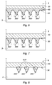
- the device 1 comprises successively the substrate 2, the metal layer 20, the filling material 6, the first layer 3, as illustrated in FIGS. Figures 6 to 8 .
- the alloy of the first and second layers 3, 5 and of the electroluminescent layer 4 is advantageously a binary alloy or a ternary alloy, the binary alloy preferably being based on GaN, the ternary alloy being preferably based on InGaN or AlGaN.
- the electroluminescent layer 4 may comprise electroluminescent sub-layers.
- the second layer 5 has an outer surface forming an interface with the output medium.
- the outer surface of the second layer 5 is advantageously textured in order to prevent a major part of the radiation produced from being trapped inside the device 1 by total internal reflections.
- the texturing of the outer surface of the second layer 5 is preferably obtained by a selective chemical attack based on KOH.
- the first and second layers 3, 5 and the electroluminescent layer 4 are preferably formed on an epitaxial growth substrate.
- the growth substrate is preferably sapphire when the spectral domain is visible; the growth substrate is preferably AlGaN when the spectral range is ultraviolet.
- the growth substrate is preferably removed by laser lift-off in the English language.
- the cavities 300 form inverted pyramid hollow patterns, generally hexagonal base (" V-pits " in English, the section being V-shaped). The peaks of the pyramids point to a dislocation or group of dislocations.
- the cavities 300 generally have a surface density between 10 8 and 10 10 cm -2 to the first surface 30 of the first layer 3. The Applicant has found that the total reflection, that is to say specular and diffuse, from radiation at the interface between the metal layer 20 and the first surface 30 of the first layer 3 decreases significantly from a surface density of the order of 10 8 cm -2 .
- the cavities 300 have a depth (that is to say the height of the pyramid) of the order of 150 nm, and a diameter (that is to say the diameter of the hexagon, substantially regular, forming the base of the pyramid) of the order of 100 nm.
- the filling material 6 forms a flat layer 60 extending between the metal layer 20 and the first surface 30 of the first layer 3, and the filling material 6 is electrically conductive.
- the filler material 6 is preferably an oxide, preferably selected from the group comprising indium tin oxide, zinc oxide ZnO doped with aluminum, indium or gallium. The doping level is adapted according to the desired level of conduction.
- the filling material 6 is deposited on the first surface 30 of the first layer 3 before the formation of the metal layer 20.
- the plane layer 60 is advantageously obtained by mechanical-chemical polishing.
- the flat layer 60 prevents any direct contact between the first layer 3 and the metal layer 20.
- the filling material 6 is flush with the first surface 30 of the first layer 3, and the first surface 30 of the first layer 3 is in contact with the metal layer 20.
- the filling material 6 is deposited on the first surface 30 of the first layer 3 before the formation of the metal layer 20. Then the outcropping is preferably obtained by mechano-chemical polishing of the filling material 6 to the first surface 30 of the first layer 3.
- the filling material 6 is advantageously selected from the group consisting of titanium dioxide TiO 2 , silicon dioxide SiO 2 , zinc oxide ZnO, zinc oxide ZnO doped with aluminum, silicon nitride SiN, indium oxide -tin.
- the metal layer 20 is in direct contact with the first layer 3 and the filling material 6.
- the filling material 6 forms dielectric balls 61, and the first surface 30 of the first layer 3 is in contact with the metal layer 20.
- dielectric beads 61 are advantageously formed by evaporation of a colloidal suspension, one of which example of implementation is given in the document T. Pinedo et al, "Assisted convective-capillary force assembly of gold colloids in a microfluid cell: Plasmonic properties of deterministic nanostructures", J. Vac. Sci. Technol., B 26 (6), 2008, p. 2513-2519 .
- This embodiment is advantageous because such a filling material 6 has a good flatness.
- Several dielectric balls 61 may also occupy a cavity 300.
- the dielectric beads 61 advantageously have a radius of between 2 nm and 20 nm so that the filling material 6 is projecting or withdrawn from the first surface 30 of the first layer 3 with a maximum distance of less than or equal to 10 nm.
- a roughness of the filling material 6 greater than 10 nm significantly degrades the reflection of the radiation at the interface between the filling material 6 and the metal layer 20. increasing absorption.
- such a radius of dielectric balls 61 much smaller than the size of the cavities 300, allows several dielectric beads 61 to occupy a cavity 300, which allows adaptation to different sizes of cavities 300.
- a dielectric ball size 61 as low as possible.
- the filler material 6 is advantageously selected from the group comprising titanium dioxide TiO 2 , silicon nitride SiN, silicon dioxide SiO 2 , zinc oxide ZnO.
Abstract
Ce dispositif comporte successivement un substrat (2) comprenant une couche métallique adaptée pour réfléchir un rayonnement ; une première couche (3) d'un alliage de type III/N, dopée de type p, et comprenant une première surface (30), en regard de la couche métallique, présentant des cavités (300) ; une couche électroluminescente d'un alliage de type III/N, adaptée pour produire le rayonnement ; une deuxième couche d'un alliage de type III/N, dopée de type n, par laquelle sort le rayonnement ; le dispositif étant remarquable en ce qu'un matériau de remplissage (6), non métallique et transparent dans le domaine spectral, est disposé à l'intérieur des cavités (300).This device comprises successively a substrate (2) comprising a metal layer adapted to reflect radiation; a first layer (3) of a type III / N type doped p-type alloy and comprising a first surface (30) opposite the metal layer, having cavities (300); an electroluminescent layer of a III / N type alloy adapted to produce the radiation; a second layer of a type III / N type n-doped alloy through which the radiation emerges; the device being remarkable in that a filling material (6), non-metallic and transparent in the spectral range, is disposed inside the cavities (300).
Description
La présente invention a trait à un dispositif électroluminescent pour émettre un rayonnement dans un domaine spectral.The present invention relates to an electroluminescent device for emitting radiation in a spectral range.
Un dispositif connu de l'état de la technique, comporte successivement :
- un substrat comprenant une couche métallique adaptée pour réfléchir le rayonnement et conduire un courant électrique ;
- une première couche d'un alliage de type III/N, dopée de type p, et comprenant une première surface, en regard de la couche métallique, présentant des cavités ;
- une couche électroluminescente d'un alliage de type III/N, adaptée pour produire le rayonnement ;
- une deuxième couche d'un alliage de type III/N, dopée de type n, par laquelle sort le rayonnement. La deuxième couche présente une surface externe formant une interface avec le milieu de sortie. La surface externe de la deuxième couche est texturée afin d'éviter qu'une majeure partie du rayonnement produit ne soit piégée à l'intérieur du dispositif par réflexions totales internes.
- a substrate comprising a metal layer adapted to reflect the radiation and conduct an electric current;
- a first layer of a type III / N type doped p-type alloy, and comprising a first surface, facing the metal layer, having cavities;
- an electroluminescent layer of a III / N type alloy adapted to produce the radiation;
- a second layer of a type III / N type n-doped alloy, through which radiation emerges. The second layer has an outer surface forming an interface with the output medium. The outer surface of the second layer is textured to prevent a major portion of the produced radiation from being trapped inside the device by total internal reflections.
Classiquement, un tel dispositif de l'état de la technique est obtenu par des épitaxies successives de la deuxième couche, de la couche électroluminescente, et de la première couche sur un substrat de croissance, en saphir ou en AlGaN. Puis, la couche métallique est formée sur les couches épitaxiées. L'ensemble est ensuite reporté sur un substrat hôte, bon conducteur de chaleur. Enfin, le substrat de croissance est supprimé par décollement laser (« Laser Lift-off » en langue anglaise). La texturation de la surface externe de la deuxième couche est obtenue par une attaque chimique sélective, à base de KOH.Conventionally, such a device of the state of the art is obtained by successive epitaxies of the second layer, the electroluminescent layer, and the first layer on a growth substrate, sapphire or AlGaN. Then, the metal layer is formed on the epitaxial layers. The assembly is then transferred to a host substrate, a good heat conductor. Finally, the growth substrate is removed by laser lift-off (" Laser Lift-off" in English). The texturing of the outer surface of the second layer is obtained by a selective chemical attack, based on KOH.
Les désaccords de mailles cristallographiques et de coefficients de dilatation thermique entre le saphir et les alliages de type III/N conduisent à des dislocations à travers les couches épitaxiées. Les dislocations se traduisent par la présence de défauts dans les couches épitaxiées. Plus précisément, les alliages de type III/N possèdent une structure cristalline hexagonale de type wurtzite, et les défauts prennent la forme de cavités, émergentes au niveau des dislocations, tout particulièrement à la première surface de la première couche. Les cavités forment classiquement des motifs creux en pyramide inversée, à base hexagonale (« V-pits » en langue anglaise) ; les sommets des pyramides pointent vers une dislocation ou un groupe de dislocations. De telles cavités forment une texturation naturelle de la première surface de la première couche, et sont remplies de métal lors de la formation de la couche métallique.Disagreements of crystallographic mesh and thermal expansion coefficients between sapphire and type III / N alloys lead to dislocations through the epitaxial layers. Dislocations result in the presence of defects in the epitaxial layers. Specifically, the III / N type alloys have a hexagonal wurtzite crystal structure, and the defects take the form of cavities, emerging at the dislocations, especially at the first surface of the first layer. The cavities form classically hollow patterns in an inverted pyramid, based on hexagonal ("V-pits" in English); the vertices of the pyramids point to a dislocation or group of dislocations. Such cavities form a natural texturing of the first surface of the first layer, and are filled with metal during the formation of the metal layer.
De telles cavités seraient intéressantes pour l'extraction de lumière, grâce à leur pouvoir diffusant, comme suggéré dans la publication
Cependant, comme illustré à la
Ainsi, la présente invention vise à remédier en tout ou partie aux inconvénients précités, et concerne à cet effet un dispositif électroluminescent pour émettre un rayonnement dans un domaine spectral, le dispositif comportant successivement :
- un substrat comprenant une couche métallique adapté pour réfléchir le rayonnement ;
- une première couche d'un alliage de type III/N, dopée de type p, et comprenant une première surface, en regard de la couche métallique, la première surface présentant des cavités ;
- une couche électroluminescente d'un alliage de type III/N, adaptée pour produire le rayonnement ;
- une deuxième couche d'un alliage de type III/N, dopée de type n, par laquelle sort le rayonnement ;
- a substrate comprising a metal layer adapted to reflect the radiation;
- a first layer of a type III / N type doped p-type alloy and comprising a first surface facing the metal layer, the first surface having cavities;
- an electroluminescent layer of a III / N type alloy adapted to produce the radiation;
- a second layer of a type III / N type n-doped alloy through which the radiation emerges;
Par « domaine spectral », on entend la longueur d'onde ou la bande de longueur d'onde du rayonnement émis. Le domaine spectral appartient préférentiellement au domaine ultraviolet ou visible.By "spectral domain" is meant the wavelength or the wavelength band of the emitted radiation. The spectral domain preferably belongs to the ultraviolet or visible domain.
Par « couche métallique », on entend une couche (ou plusieurs sous-couches) d'un matériau métallique, le matériau métallique pouvant être un métal pur ou un alliage métallique."Metal layer" means a layer (or more sub-layers) of a metallic material, the metal material may be a pure metal or a metal alloy.
Par « alliage de type III/N », on entend un nitrure d'au moins un élément situé dans la colonne III du tableau périodique des éléments."Type III / N alloy" means a nitride of at least one element located in column III of the Periodic Table of the Elements.
Par « dopé de type p (respectivement n) », on entend que l'alliage correspondant comporte des impuretés adaptées pour favoriser une conduction électrique par des trous (respectivement par des électrons).By "doped p-type (respectively n)" is meant that the corresponding alloy comprises impurities adapted to promote electrical conduction through holes (respectively by electrons).
Par « transparent », on entend que le matériau de remplissage présente un coefficient d'extinction inférieur ou égal à 0,1 dans le domaine spectral.By "transparent" it is meant that the filler material has an extinction coefficient of less than or equal to 0.1 in the spectral range.
Ainsi, un tel dispositif selon l'invention permet, par rapport à l'état de la technique, de réduire les pertes d'absorption à l'interface entre la couche métallique et la première surface de la première couche, et ce grâce à un tel matériau de remplissage. Un tel dispositif selon l'invention permet par là-même d'augmenter la réflexion totale du rayonnement à ladite interface, et donc l'extraction de lumière. Les pertes d'absorption sont d'autant plus réduites que la densité surfacique de cavités à la première surface est élevée. Le matériau de remplissage est non métallique de manière à également éviter un couplage optique entre le rayonnement produit par la couche électroluminescente et des plasmons de surface à la première surface de la première couche.Thus, such a device according to the invention makes it possible, compared with the state of the art, to reduce the absorption losses at the interface between the metal layer and the first surface of the first layer, thanks to a such filling material. Such a device according to the invention thus makes it possible to increase the total reflection of the radiation at said interface, and thus the light extraction. Absorption losses are even smaller as the surface density of cavities at the first surface is high. The filler material is non-metallic so as to also avoid optical coupling between the radiation produced by the electroluminescent layer and surface plasmons at the first surface of the first layer.
Dans un mode de réalisation, le matériau de remplissage forme une couche plane s'étendant entre la couche métallique et la première surface de la première couche, et le matériau de remplissage est électriquement conducteur.In one embodiment, the filler material forms a planar layer extending between the metal layer and the first surface of the first layer, and the filler material is electrically conductive.
Par « électriquement conducteur », on entend que le matériau de remplissage présente une conductivité électrique à 300 K comprise entre 103 et 104 S/cm.By "electrically conductive" is meant that the filler material has an electrical conductivity at 300 K between 10 3 and 10 4 S / cm.
Ainsi, une telle couche plane, intercalée entre la première surface de la première couche et la couche métallique, permet d'éviter un aplanissement de la première surface de la première couche (par exemple par polissage mécano-chimique), et par là-même d'éviter une dégradation des performances électriques de la première couche. Une telle couche plane empêche tout contact direct entre la première surface de la première couche et la couche métallique. Le matériau de remplissage est donc électriquement conducteur pour permettre la polarisation du dispositif.Thus, such a plane layer, interposed between the first surface of the first layer and the metal layer, avoids a flattening of the first surface of the first layer (for example by chemical mechanical polishing), and thereby to avoid degradation of electrical performance of the first layer. Such a flat layer prevents any direct contact between the first surface of the first layer and the metal layer. The filler material is electrically conductive to allow polarization of the device.
Avantageusement, le matériau de remplissage est un oxyde, de préférence sélectionné dans le groupe comportant l'oxyde d'indium-étain, l'oxyde de zinc ZnO dopé à l'aluminium, à l'indium ou au gallium.Advantageously, the filling material is an oxide, preferably selected from the group comprising indium tin oxide, zinc oxide ZnO doped with aluminum, indium or gallium.
Ainsi, de tels matériaux sont à la fois électriquement conducteurs et présentent un indice optique proche de celui d'un alliage de type III/N, par exemple le GaN (n=2,45 à 450 nm). En outre, de tels oxydes transparents conducteurs peuvent être formés simplement à la première surface de la première couche. L'oxyde d'indium-étain est particulièrement avantageux car c'est un excellent injecteur de trous.Thus, such materials are both electrically conductive and have an optical index close to that of a type III / N alloy, for example GaN (n = 2.45 at 450 nm). In addition, such transparent conductive oxides can be formed simply at the first surface of the first layer. Indium tin oxide is particularly advantageous because it is an excellent injector of holes.
Dans un mode de réalisation, le matériau de remplissage affleure la première surface de la première couche, et la première surface de la première couche est en contact avec la couche métallique.In one embodiment, the filler material is flush with the first surface of the first layer, and the first surface of the first layer is in contact with the metal layer.
Ainsi, une plus grande liberté sur le choix du matériau de remplissage est autorisée car la conduction électrique est assurée par la première couche. Le matériau de remplissage peut donc être un matériau électriquement conducteur ou un matériau diélectrique.Thus, greater freedom in the choice of filling material is allowed because the electrical conduction is provided by the first layer. The filler material may therefore be an electrically conductive material or a dielectric material.
Par « diélectrique », on entend que le matériau de remplissage présente une conductivité électrique à 300 K strictement inférieure à 10-8 S/cm.By "dielectric" is meant that the filling material has an electrical conductivity at 300 K strictly less than 10 -8 S / cm.
Par « affleure », on entend que le matériau de remplissage :
- arrive au niveau de la première surface de la première couche, ou
- est en saillie ou en retrait de la première surface de la première couche avec une distance maximale inférieure ou égale à 10 nm.
- reaches the level of the first surface of the first layer, or
- is projecting or withdrawing from the first surface of the first layer with a maximum distance of less than or equal to 10 nm.
Avantageusement, le matériau de remplissage est sélectionné dans le groupe comportant le dioxyde de titane TiO2, le dioxyde de silicium SiO2, l'oxyde de zinc ZnO, l'oxyde de zinc ZnO dopé à l'aluminium, à l'indium ou au gallium, le nitrure de silicium SiN, l'oxyde d'indium-étain.Advantageously, the filling material is selected from the group comprising titanium dioxide TiO 2 , silicon dioxide SiO 2 , zinc oxide ZnO, zinc oxide ZnO doped with aluminum, with indium or gallium, silicon nitride SiN, indium-tin oxide.
Ainsi, de tels matériaux de remplissage présentent un indice optique proche de celui d'un alliage de type III/N, par exemple le GaN (n=2,45 à 450 nm), et peuvent être formés simplement à l'intérieur des cavités.Thus, such filler materials have an optical index close to that of a type III / N alloy, for example GaN (n = 2.45 at 450 nm), and can be formed simply inside the cavities .
Dans un mode de réalisation, le matériau de remplissage forme des billes diélectriques, et la première surface de la première couche est en contact avec la couche métallique.In one embodiment, the filler material forms dielectric beads, and the first surface of the first layer is in contact with the metal layer.
De telles billes diélectriques sont avantageusement formées par une évaporation d'une suspension colloïdale.Such dielectric beads are advantageously formed by evaporation of a colloidal suspension.
Avantageusement, le matériau de remplissage est sélectionné dans le groupe comportant le dioxyde de titane TiO2, le nitrure de silicium SiN, le dioxyde de silicium SiO2, l'oxyde de zinc ZnO.Advantageously, the filling material is selected from the group comprising titanium dioxide TiO 2 , silicon nitride SiN, silicon dioxide SiO 2 , zinc oxide ZnO.
Avantageusement, la couche métallique est à base d'argent ou d'aluminium.Advantageously, the metal layer is based on silver or aluminum.
Avantageusement, l'alliage des première et deuxième couches et de la couche électroluminescente est un alliage binaire ou un alliage ternaire, l'alliage binaire étant de préférence à base de GaN, l'alliage ternaire étant de préférence à base d'InGaN ou d'AlGaN.Advantageously, the alloy of the first and second layers and of the electroluminescent layer is a binary alloy or a ternary alloy, the binary alloy preferably being based on GaN, the ternary alloy being preferably based on InGaN or AlGaN.
Avantageusement, les cavités présentent une densité surfacique supérieure à 108 cm-2 à la première surface de la première couche.Advantageously, the cavities have a surface density greater than 10 8 cm -2 at the first surface of the first layer.
D'autres caractéristiques et avantages apparaîtront dans la description qui va suivre de différents modes de réalisation de l'invention, donnés à titre d'exemples non limitatifs, en référence aux dessins annexés dans lesquels :
- la
figure 1 est une vue schématique en perspective d'un dispositif selon l'invention, - la
figure 2 est une vue schématique partielle en coupe d'un dispositif selon un premier mode de réalisation de l'invention, - la
figure 3 est une vue schématique partielle en coupe d'un dispositif selon un deuxième mode de réalisation de l'invention, - la
figure 4 est une vue schématique partielle en coupe d'un dispositif selon un troisième mode de réalisation de l'invention, - la
figure 5 (déjà commentée) est un graphique représentant la réflectivité totale de l'interface entre la couche métallique (en Ag) et la première surface de la première couche (en GaN) d'un dispositif de l'état de la technique (axe des ordonnées, en %) en fonction de la longueur d'onde du rayonnement émis (axe des abscisses, en nm), pour différentes densités d de cavités (A : d=2.109 cm-2, B : d=109 cm-2, C : d=2.108 cm-2, D : d=0), - la
figure 6 est une vue schématique partielle en coupe d'un dispositif selon le premier mode de réalisation illustrant la couche métallique, - la
figure 7 est une vue schématique partielle en coupe d'un dispositif selon le deuxième mode de réalisation illustrant la couche métallique, - la
figure 8 est une vue schématique partielle en coupe d'un dispositif selon le troisième mode de réalisation illustrant la couche métallique.
- the
figure 1 is a schematic perspective view of a device according to the invention, - the
figure 2 is a partial schematic sectional view of a device according to a first embodiment of the invention, - the
figure 3 is a partial schematic sectional view of a device according to a second embodiment of the invention, - the
figure 4 is a partial schematic sectional view of a device according to a third embodiment of the invention, - the
figure 5 (already commented) is a graph representing the total reflectivity of the interface between the metal layer (in Ag) and the first surface of the first layer (in GaN) of a device of the state of the art (ordinate axis , in%) as a function of the wavelength of the emitted radiation (abscissa axis, in nm), for different densities d of cavities (A: d = 2.10 9 cm -2 , B: d = 10 9 cm -2 , C: d = 2.10 8 cm -2 , D: d = 0), - the
figure 6 is a partial schematic sectional view of a device according to the first embodiment illustrating the metal layer, - the
figure 7 is a partial schematic sectional view of a device according to the second embodiment illustrating the metal layer, - the
figure 8 is a partial schematic sectional view of a device according to the third embodiment illustrating the metal layer.
Pour les différents modes de réalisation, les mêmes références seront utilisées pour des éléments identiques ou assurant la même fonction, par souci de simplification de la description. Les caractéristiques techniques décrites ci-après pour différents modes de réalisation sont à considérer isolément ou selon toute combinaison techniquement possible.For the different embodiments, the same references will be used for identical elements or ensuring the same function, for the sake of simplification of the description. The technical characteristics described below for different embodiments are to be considered in isolation or in any technically possible combination.
Le dispositif illustré aux
un substrat 2 comprenant une couche métallique 20 adaptée pour réfléchir le rayonnement ;- une première couche 3 d'un alliage de type III/N, dopée de type p, et comprenant une première
surface 30, en regard de la couche métallique 20,la première surface 30 présentant des cavités 300 ; - une couche électroluminescente 4 d'un alliage de type III/N, adaptée pour produire le rayonnement ;
- une deuxième couche 5 d'un alliage de type III/N, dopée de type n, par laquelle sort le rayonnement.
- a
substrate 2 comprising ametal layer 20 adapted to reflect the radiation; - a
first layer 3 of a type III / N type doped p-type alloy and comprising afirst surface 30 facing themetal layer 20, thefirst surface 30 havingcavities 300; - an
electroluminescent layer 4 of a III / N type alloy, adapted to produce the radiation; - a
second layer 5 of a type III / N type n-doped alloy, through which the radiation emerges.
Un matériau de remplissage 6, non métallique et transparent dans le domaine spectral, est disposé à l'intérieur des cavités 300. Le matériau de remplissage 6 est différent du matériau du substrat 2.A filling
Un plot de contact 7 est avantageusement formé sur la deuxième couche 5.A
Le dispositif 1 est préférentiellement une diode électroluminescente, plus préférentiellement à technologie VTF (pour Vertical Thin Film en langue anglaise) ou à technologie TFFC (pour Thin Film Flip Chip). Le domaine spectral est préférentiellement le domaine ultraviolet ou visible, compris entre 200 nm et 780 nm.The
La couche métallique 20 est d'un matériau métallique, le matériau métallique étant un métal pur ou un alliage métallique. Le matériau métallique est avantageusement à base d'argent ou d'aluminium. La couche métallique 20 peut comporter des sous-couches d'un matériau métallique. La couche métallique 20 forme un miroir réflecteur adapté pour réfléchir le rayonnement. La couche métallique 20 présente avantageusement un coefficient de réflexion supérieure à 0,8, préférentiellement supérieur à 0,9, afin d'obtenir un rendement d'extraction optique élevé. La couche métallique 20 est adaptée pour conduire un courant électrique. La couche métallique 20 permet la polarisation du dispositif 1 par injection de porteurs.The
La couche métallique 20 s'étend au moins partiellement en contact avec le matériau de remplissage 6. La couche métallique 20 s'étend entre le substrat 2 et le matériau de remplissage 6. En d'autres termes, le dispositif 1 comporte successivement le substrat 2, la couche métallique 20, le matériau de remplissage 6, la première couche 3, comme illustré aux
L'alliage des première et deuxième couches 3, 5 et de la couche électroluminescente 4 est avantageusement un alliage binaire ou un alliage ternaire, l'alliage binaire étant de préférence à base de GaN, l'alliage ternaire étant de préférence à base d'InGaN ou d'AlGaN. La couche électroluminescente 4 peut comporter des sous-couches électroluminescentes. La deuxième couche 5 présente une surface externe formant une interface avec le milieu de sortie. La surface externe de la deuxième couche 5 est avantageusement texturée afin d'éviter qu'une majeure partie du rayonnement produit ne soit piégée à l'intérieur du dispositif 1 par réflexions totales internes. La texturation de la surface externe de la deuxième couche 5 est préférentiellement obtenue par une attaque chimique sélective, à base de KOH. Les première et deuxième couches 3, 5 et la couche électroluminescente 4 sont préférentiellement formées sur un substrat de croissance par épitaxie. Le substrat de croissance est de préférence en saphir lorsque le domaine spectral est le visible ; le substrat de croissance est de préférence en AlGaN lorsque le domaine spectral est l'ultraviolet. Après la formation de la couche métallique 20 et du report de l'ensemble sur le substrat 2 (substrat hôte), le substrat de croissance est préférentiellement supprimé par décollement laser (« Laser Lift-off » en langue anglaise).The alloy of the first and
Les cavités 300 forment des motifs creux en pyramide inversée, généralement à base hexagonale (« V-pits » en langue anglaise, la section étant en forme de V). Les sommets des pyramides pointent vers une dislocation ou un groupe de dislocations. Les cavités 300 présentent généralement une densité surfacique comprise entre 108 et 1010 cm-2 à la première surface 30 de la première couche 3. La demanderesse a constaté que la réflexion totale, c'est-à-dire spéculaire et diffuse, du rayonnement à l'interface entre la couche métallique 20 et la première surface 30 de la première couche 3 diminue significativement à partir d'une densité surfacique de l'ordre de 108 cm-2. Les cavités 300 présentent une profondeur (c'est-à-dire la hauteur de la pyramide) de l'ordre de 150 nm, et un diamètre (c'est-à-dire le diamètre de l'hexagone, sensiblement régulier, formant la base de la pyramide) de l'ordre de 100 nm.The
Dans un mode de réalisation illustré à la
Dans un mode de réalisation illustré à la
Dans un mode de réalisation illustré à la
Claims (10)
Applications Claiming Priority (1)
| Application Number | Priority Date | Filing Date | Title |
|---|---|---|---|
| FR1556152A FR3038451B1 (en) | 2015-06-30 | 2015-06-30 | ELECTROLUMINESCENT DEVICE. |
Publications (2)
| Publication Number | Publication Date |
|---|---|
| EP3113235A1 true EP3113235A1 (en) | 2017-01-04 |
| EP3113235B1 EP3113235B1 (en) | 2021-09-08 |
Family
ID=54478141
Family Applications (1)
| Application Number | Title | Priority Date | Filing Date |
|---|---|---|---|
| EP16176191.1A Active EP3113235B1 (en) | 2015-06-30 | 2016-06-24 | Electroluminescent device |
Country Status (3)
| Country | Link |
|---|---|
| US (1) | US10186636B2 (en) |
| EP (1) | EP3113235B1 (en) |
| FR (1) | FR3038451B1 (en) |
Cited By (1)
| Publication number | Priority date | Publication date | Assignee | Title |
|---|---|---|---|---|
| WO2021037457A1 (en) * | 2019-08-27 | 2021-03-04 | Osram Opto Semiconductors Gmbh | Semiconductor chip and method for producing a semiconductor chip |
Families Citing this family (1)
| Publication number | Priority date | Publication date | Assignee | Title |
|---|---|---|---|---|
| DE102017105397A1 (en) | 2017-03-14 | 2018-09-20 | Osram Opto Semiconductors Gmbh | Process for the production of light emitting diodes and light emitting diode |
Citations (5)
| Publication number | Priority date | Publication date | Assignee | Title |
|---|---|---|---|---|
| US6657236B1 (en) * | 1999-12-03 | 2003-12-02 | Cree Lighting Company | Enhanced light extraction in LEDs through the use of internal and external optical elements |
| US20080303047A1 (en) * | 2007-05-15 | 2008-12-11 | Epistar Corporation | Light-emitting diode device and manufacturing method therof |
| US20120280260A1 (en) * | 2008-11-17 | 2012-11-08 | Hyung Jo Park | Semiconductor light emitting device |
| US20120299040A1 (en) * | 2011-05-23 | 2012-11-29 | Samsung Electronics Co., Ltd. | Semiconductor light emitting device and method of manufacturing the same |
| US20140175474A1 (en) * | 2012-12-21 | 2014-06-26 | Samsung Electronics Co., Ltd. | Semiconductor light emitting device and method of manufacturing the same |
Family Cites Families (1)
| Publication number | Priority date | Publication date | Assignee | Title |
|---|---|---|---|---|
| US9508902B2 (en) * | 2005-02-21 | 2016-11-29 | Epistar Corporation | Optoelectronic semiconductor device |
-
2015
- 2015-06-30 FR FR1556152A patent/FR3038451B1/en not_active Expired - Fee Related
-
2016
- 2016-06-24 EP EP16176191.1A patent/EP3113235B1/en active Active
- 2016-06-30 US US15/199,152 patent/US10186636B2/en active Active
Patent Citations (5)
| Publication number | Priority date | Publication date | Assignee | Title |
|---|---|---|---|---|
| US6657236B1 (en) * | 1999-12-03 | 2003-12-02 | Cree Lighting Company | Enhanced light extraction in LEDs through the use of internal and external optical elements |
| US20080303047A1 (en) * | 2007-05-15 | 2008-12-11 | Epistar Corporation | Light-emitting diode device and manufacturing method therof |
| US20120280260A1 (en) * | 2008-11-17 | 2012-11-08 | Hyung Jo Park | Semiconductor light emitting device |
| US20120299040A1 (en) * | 2011-05-23 | 2012-11-29 | Samsung Electronics Co., Ltd. | Semiconductor light emitting device and method of manufacturing the same |
| US20140175474A1 (en) * | 2012-12-21 | 2014-06-26 | Samsung Electronics Co., Ltd. | Semiconductor light emitting device and method of manufacturing the same |
Non-Patent Citations (2)
| Title |
|---|
| C.M. TSAI ET AL.: "Photonics Technology Letters", vol. 18, 2006, IEEE, article "High efficiency and improved ESD characteristics of GaN-based LEDs with naturally textured surface grown by MOCVD", pages: 1213 - 1215 |
| T. PINEDO ET AL.: "Assisted convective-capillary force assembly of gold colloids in a microfluid ce// : Plasmonic properties of deterministic nanostructures", J. VAC. SCI. TECHNOL., B, vol. 26, no. 6, 2008, pages 2513 - 2519, XP012114504, DOI: doi:10.1116/1.3021396 |
Cited By (1)
| Publication number | Priority date | Publication date | Assignee | Title |
|---|---|---|---|---|
| WO2021037457A1 (en) * | 2019-08-27 | 2021-03-04 | Osram Opto Semiconductors Gmbh | Semiconductor chip and method for producing a semiconductor chip |
Also Published As
| Publication number | Publication date |
|---|---|
| EP3113235B1 (en) | 2021-09-08 |
| FR3038451A1 (en) | 2017-01-06 |
| US10186636B2 (en) | 2019-01-22 |
| US20170005230A1 (en) | 2017-01-05 |
| FR3038451B1 (en) | 2017-07-21 |
Similar Documents
| Publication | Publication Date | Title |
|---|---|---|
| EP2203939B1 (en) | Optoelectronic device including nanowires, and corresponding methods | |
| EP2715808B1 (en) | Semiconductor structure for emitting light, and method for manufacturing such a structure | |
| JP5623074B2 (en) | Optoelectronic semiconductor parts | |
| EP3373345B1 (en) | Optoelectronic device comprising light-emitting diodes with improved light extraction | |
| FR2964796A1 (en) | Optoelectronic light emitting device i.e. gallium nitride based LED, has p-doped planarized layer allowing radial injection of holes in nanowire, and n-type silicon substrate allowing axial injection of electrons in nanowire | |
| FR2923651A1 (en) | PN junction forming method for nanowire of e.g. LED, involves polarizing conductor element such that regions are created in nanowire, where regions comprise conductivity carriers provided with PN junction between them | |
| FR2967813A1 (en) | METHOD FOR PRODUCING A BENTALLIC METAL LAYER STRUCTURE | |
| FR2988904A1 (en) | OPTOELECTRONIC NANOWIL SEMICONDUCTOR STRUCTURE AND METHOD OF MANUFACTURING SUCH STRUCTURE | |
| FR2964498A1 (en) | Semiconductor light-emitting plate for use in e.g. computer screen, has first and second light-emitting layers that are connected together by molecular bonding without requiring any adhesive | |
| FR3044470A1 (en) | OPTOELECTRONIC DEVICE COMPRISING THREE DIMENSIONAL SEMICONDUCTOR STRUCTURES IN AXIAL CONFIGURATION | |
| EP3503222A1 (en) | Method for manufacturing an optoelectronic device by transferring a conversion structure onto an emission structure | |
| EP3113235B1 (en) | Electroluminescent device | |
| EP3130010B1 (en) | Optoelectronic device with improved emission diagram comprising light emitting diodes | |
| EP2800151B1 (en) | Optoelectronic arrangement provided with a semiconductor nanowire in which one longitudinal section is surrounded by a mirror portion | |
| WO2013102664A1 (en) | Structured substrate for leds with high light extraction | |
| EP3843162B1 (en) | Method for manufacturing a light-emitting diode with extraction layer comprising a step of sizing of a semiconductor layer | |
| US20120241788A1 (en) | Textured Light Emitting Devices and Methods of Making the Same | |
| WO2021130136A1 (en) | Laser treatment device and laser treatment method | |
| WO2020083757A1 (en) | Optoelectronic device comprising light-emitting diodes with improved light extraction | |
| EP3843161B1 (en) | Method for manufacturing a light-emitting diode comprising a step of sizing of a semiconductor layer | |
| Zhou et al. | Enhancement in light output power of LEDs with reflective current blocking layer and backside hybrid reflector | |
| EP2827390A1 (en) | Emissive structure with lateral injection of carriers | |
| FR3105878A1 (en) | Device with three-dimensional optoelectronic components for laser cutting and method of laser cutting of such a device | |
| WO2021209460A1 (en) | Method for manufacturing a device for emitting radiation | |
| FR2979436A1 (en) | REFLECTOR DEVICE FOR REAR FRONT OF OPTICAL DEVICES |
Legal Events
| Date | Code | Title | Description |
|---|---|---|---|
| PUAI | Public reference made under article 153(3) epc to a published international application that has entered the european phase |
Free format text: ORIGINAL CODE: 0009012 |
|
| STAA | Information on the status of an ep patent application or granted ep patent |
Free format text: STATUS: EXAMINATION IS IN PROGRESS |
|
| 17P | Request for examination filed |
Effective date: 20160624 |
|
| AK | Designated contracting states |
Kind code of ref document: A1 Designated state(s): AL AT BE BG CH CY CZ DE DK EE ES FI FR GB GR HR HU IE IS IT LI LT LU LV MC MK MT NL NO PL PT RO RS SE SI SK SM TR |
|
| AX | Request for extension of the european patent |
Extension state: BA ME |
|
| STAA | Information on the status of an ep patent application or granted ep patent |
Free format text: STATUS: EXAMINATION IS IN PROGRESS |
|
| RBV | Designated contracting states (corrected) |
Designated state(s): AL AT BE BG CH CY CZ DE DK EE ES FI FR GB GR HR HU IE IS IT LI LT LU LV MC MK MT NL NO PL PT RO RS SE SI SK SM TR |
|
| GRAP | Despatch of communication of intention to grant a patent |
Free format text: ORIGINAL CODE: EPIDOSNIGR1 |
|
| STAA | Information on the status of an ep patent application or granted ep patent |
Free format text: STATUS: GRANT OF PATENT IS INTENDED |
|
| INTG | Intention to grant announced |
Effective date: 20210407 |
|
| GRAS | Grant fee paid |
Free format text: ORIGINAL CODE: EPIDOSNIGR3 |
|
| GRAA | (expected) grant |
Free format text: ORIGINAL CODE: 0009210 |
|
| STAA | Information on the status of an ep patent application or granted ep patent |
Free format text: STATUS: THE PATENT HAS BEEN GRANTED |
|
| AK | Designated contracting states |
Kind code of ref document: B1 Designated state(s): AL AT BE BG CH CY CZ DE DK EE ES FI FR GB GR HR HU IE IS IT LI LT LU LV MC MK MT NL NO PL PT RO RS SE SI SK SM TR |
|
| REG | Reference to a national code |
Ref country code: GB Ref legal event code: FG4D Free format text: NOT ENGLISH |
|
| REG | Reference to a national code |
Ref country code: AT Ref legal event code: REF Ref document number: 1429358 Country of ref document: AT Kind code of ref document: T Effective date: 20210915 Ref country code: CH Ref legal event code: EP |
|
| REG | Reference to a national code |
Ref country code: IE Ref legal event code: FG4D Free format text: LANGUAGE OF EP DOCUMENT: FRENCH |
|
| REG | Reference to a national code |
Ref country code: DE Ref legal event code: R096 Ref document number: 602016063365 Country of ref document: DE |
|
| REG | Reference to a national code |
Ref country code: LT Ref legal event code: MG9D |
|
| REG | Reference to a national code |
Ref country code: NL Ref legal event code: MP Effective date: 20210908 |
|
| PG25 | Lapsed in a contracting state [announced via postgrant information from national office to epo] |
Ref country code: LT Free format text: LAPSE BECAUSE OF FAILURE TO SUBMIT A TRANSLATION OF THE DESCRIPTION OR TO PAY THE FEE WITHIN THE PRESCRIBED TIME-LIMIT Effective date: 20210908 Ref country code: BG Free format text: LAPSE BECAUSE OF FAILURE TO SUBMIT A TRANSLATION OF THE DESCRIPTION OR TO PAY THE FEE WITHIN THE PRESCRIBED TIME-LIMIT Effective date: 20211208 Ref country code: NO Free format text: LAPSE BECAUSE OF FAILURE TO SUBMIT A TRANSLATION OF THE DESCRIPTION OR TO PAY THE FEE WITHIN THE PRESCRIBED TIME-LIMIT Effective date: 20211208 Ref country code: FI Free format text: LAPSE BECAUSE OF FAILURE TO SUBMIT A TRANSLATION OF THE DESCRIPTION OR TO PAY THE FEE WITHIN THE PRESCRIBED TIME-LIMIT Effective date: 20210908 Ref country code: ES Free format text: LAPSE BECAUSE OF FAILURE TO SUBMIT A TRANSLATION OF THE DESCRIPTION OR TO PAY THE FEE WITHIN THE PRESCRIBED TIME-LIMIT Effective date: 20210908 Ref country code: SE Free format text: LAPSE BECAUSE OF FAILURE TO SUBMIT A TRANSLATION OF THE DESCRIPTION OR TO PAY THE FEE WITHIN THE PRESCRIBED TIME-LIMIT Effective date: 20210908 Ref country code: RS Free format text: LAPSE BECAUSE OF FAILURE TO SUBMIT A TRANSLATION OF THE DESCRIPTION OR TO PAY THE FEE WITHIN THE PRESCRIBED TIME-LIMIT Effective date: 20210908 Ref country code: HR Free format text: LAPSE BECAUSE OF FAILURE TO SUBMIT A TRANSLATION OF THE DESCRIPTION OR TO PAY THE FEE WITHIN THE PRESCRIBED TIME-LIMIT Effective date: 20210908 |
|
| REG | Reference to a national code |
Ref country code: AT Ref legal event code: MK05 Ref document number: 1429358 Country of ref document: AT Kind code of ref document: T Effective date: 20210908 |
|
| PG25 | Lapsed in a contracting state [announced via postgrant information from national office to epo] |
Ref country code: LV Free format text: LAPSE BECAUSE OF FAILURE TO SUBMIT A TRANSLATION OF THE DESCRIPTION OR TO PAY THE FEE WITHIN THE PRESCRIBED TIME-LIMIT Effective date: 20210908 Ref country code: GR Free format text: LAPSE BECAUSE OF FAILURE TO SUBMIT A TRANSLATION OF THE DESCRIPTION OR TO PAY THE FEE WITHIN THE PRESCRIBED TIME-LIMIT Effective date: 20211209 |
|
| PG25 | Lapsed in a contracting state [announced via postgrant information from national office to epo] |
Ref country code: AT Free format text: LAPSE BECAUSE OF FAILURE TO SUBMIT A TRANSLATION OF THE DESCRIPTION OR TO PAY THE FEE WITHIN THE PRESCRIBED TIME-LIMIT Effective date: 20210908 |
|
| PG25 | Lapsed in a contracting state [announced via postgrant information from national office to epo] |
Ref country code: IS Free format text: LAPSE BECAUSE OF FAILURE TO SUBMIT A TRANSLATION OF THE DESCRIPTION OR TO PAY THE FEE WITHIN THE PRESCRIBED TIME-LIMIT Effective date: 20220108 Ref country code: SM Free format text: LAPSE BECAUSE OF FAILURE TO SUBMIT A TRANSLATION OF THE DESCRIPTION OR TO PAY THE FEE WITHIN THE PRESCRIBED TIME-LIMIT Effective date: 20210908 Ref country code: SK Free format text: LAPSE BECAUSE OF FAILURE TO SUBMIT A TRANSLATION OF THE DESCRIPTION OR TO PAY THE FEE WITHIN THE PRESCRIBED TIME-LIMIT Effective date: 20210908 Ref country code: RO Free format text: LAPSE BECAUSE OF FAILURE TO SUBMIT A TRANSLATION OF THE DESCRIPTION OR TO PAY THE FEE WITHIN THE PRESCRIBED TIME-LIMIT Effective date: 20210908 Ref country code: PT Free format text: LAPSE BECAUSE OF FAILURE TO SUBMIT A TRANSLATION OF THE DESCRIPTION OR TO PAY THE FEE WITHIN THE PRESCRIBED TIME-LIMIT Effective date: 20220110 Ref country code: PL Free format text: LAPSE BECAUSE OF FAILURE TO SUBMIT A TRANSLATION OF THE DESCRIPTION OR TO PAY THE FEE WITHIN THE PRESCRIBED TIME-LIMIT Effective date: 20210908 Ref country code: NL Free format text: LAPSE BECAUSE OF FAILURE TO SUBMIT A TRANSLATION OF THE DESCRIPTION OR TO PAY THE FEE WITHIN THE PRESCRIBED TIME-LIMIT Effective date: 20210908 Ref country code: EE Free format text: LAPSE BECAUSE OF FAILURE TO SUBMIT A TRANSLATION OF THE DESCRIPTION OR TO PAY THE FEE WITHIN THE PRESCRIBED TIME-LIMIT Effective date: 20210908 Ref country code: CZ Free format text: LAPSE BECAUSE OF FAILURE TO SUBMIT A TRANSLATION OF THE DESCRIPTION OR TO PAY THE FEE WITHIN THE PRESCRIBED TIME-LIMIT Effective date: 20210908 Ref country code: AL Free format text: LAPSE BECAUSE OF FAILURE TO SUBMIT A TRANSLATION OF THE DESCRIPTION OR TO PAY THE FEE WITHIN THE PRESCRIBED TIME-LIMIT Effective date: 20210908 |
|
| REG | Reference to a national code |
Ref country code: DE Ref legal event code: R097 Ref document number: 602016063365 Country of ref document: DE |
|
| PLBE | No opposition filed within time limit |
Free format text: ORIGINAL CODE: 0009261 |
|
| STAA | Information on the status of an ep patent application or granted ep patent |
Free format text: STATUS: NO OPPOSITION FILED WITHIN TIME LIMIT |
|
| PG25 | Lapsed in a contracting state [announced via postgrant information from national office to epo] |
Ref country code: DK Free format text: LAPSE BECAUSE OF FAILURE TO SUBMIT A TRANSLATION OF THE DESCRIPTION OR TO PAY THE FEE WITHIN THE PRESCRIBED TIME-LIMIT Effective date: 20210908 |
|
| 26N | No opposition filed |
Effective date: 20220609 |
|
| PG25 | Lapsed in a contracting state [announced via postgrant information from national office to epo] |
Ref country code: SI Free format text: LAPSE BECAUSE OF FAILURE TO SUBMIT A TRANSLATION OF THE DESCRIPTION OR TO PAY THE FEE WITHIN THE PRESCRIBED TIME-LIMIT Effective date: 20210908 |
|
| PG25 | Lapsed in a contracting state [announced via postgrant information from national office to epo] |
Ref country code: MC Free format text: LAPSE BECAUSE OF FAILURE TO SUBMIT A TRANSLATION OF THE DESCRIPTION OR TO PAY THE FEE WITHIN THE PRESCRIBED TIME-LIMIT Effective date: 20210908 Ref country code: IT Free format text: LAPSE BECAUSE OF FAILURE TO SUBMIT A TRANSLATION OF THE DESCRIPTION OR TO PAY THE FEE WITHIN THE PRESCRIBED TIME-LIMIT Effective date: 20210908 |
|
| REG | Reference to a national code |
Ref country code: CH Ref legal event code: PL |
|
| REG | Reference to a national code |
Ref country code: BE Ref legal event code: MM Effective date: 20220630 |
|
| PG25 | Lapsed in a contracting state [announced via postgrant information from national office to epo] |
Ref country code: LU Free format text: LAPSE BECAUSE OF NON-PAYMENT OF DUE FEES Effective date: 20220624 Ref country code: LI Free format text: LAPSE BECAUSE OF NON-PAYMENT OF DUE FEES Effective date: 20220630 Ref country code: IE Free format text: LAPSE BECAUSE OF NON-PAYMENT OF DUE FEES Effective date: 20220624 Ref country code: CH Free format text: LAPSE BECAUSE OF NON-PAYMENT OF DUE FEES Effective date: 20220630 |
|
| PG25 | Lapsed in a contracting state [announced via postgrant information from national office to epo] |
Ref country code: BE Free format text: LAPSE BECAUSE OF NON-PAYMENT OF DUE FEES Effective date: 20220630 |
|
| PGFP | Annual fee paid to national office [announced via postgrant information from national office to epo] |
Ref country code: FR Payment date: 20230626 Year of fee payment: 8 Ref country code: DE Payment date: 20230620 Year of fee payment: 8 |
|
| PGFP | Annual fee paid to national office [announced via postgrant information from national office to epo] |
Ref country code: GB Payment date: 20230622 Year of fee payment: 8 |
|
| PG25 | Lapsed in a contracting state [announced via postgrant information from national office to epo] |
Ref country code: HU Free format text: LAPSE BECAUSE OF FAILURE TO SUBMIT A TRANSLATION OF THE DESCRIPTION OR TO PAY THE FEE WITHIN THE PRESCRIBED TIME-LIMIT; INVALID AB INITIO Effective date: 20160624 |