EP3112973A1 - Constant voltage supplying circuit for circuit breaker - Google Patents
Constant voltage supplying circuit for circuit breaker Download PDFInfo
- Publication number
- EP3112973A1 EP3112973A1 EP16166837.1A EP16166837A EP3112973A1 EP 3112973 A1 EP3112973 A1 EP 3112973A1 EP 16166837 A EP16166837 A EP 16166837A EP 3112973 A1 EP3112973 A1 EP 3112973A1
- Authority
- EP
- European Patent Office
- Prior art keywords
- current
- circuit
- voltage
- constant voltage
- switching device
- Prior art date
- Legal status (The legal status is an assumption and is not a legal conclusion. Google has not performed a legal analysis and makes no representation as to the accuracy of the status listed.)
- Withdrawn
Links
- 229910044991 metal oxide Inorganic materials 0.000 claims description 3
- 150000004706 metal oxides Chemical class 0.000 claims description 3
- 239000004065 semiconductor Substances 0.000 claims description 3
- 238000010586 diagram Methods 0.000 description 7
- 239000008186 active pharmaceutical agent Substances 0.000 description 3
- 238000001514 detection method Methods 0.000 description 2
- 230000004048 modification Effects 0.000 description 2
- 238000012986 modification Methods 0.000 description 2
- 239000003990 capacitor Substances 0.000 description 1
- 230000005415 magnetization Effects 0.000 description 1
- 230000006641 stabilisation Effects 0.000 description 1
- 238000011105 stabilization Methods 0.000 description 1
Images


Classifications
-
- H—ELECTRICITY
- H01—ELECTRIC ELEMENTS
- H01H—ELECTRIC SWITCHES; RELAYS; SELECTORS; EMERGENCY PROTECTIVE DEVICES
- H01H47/00—Circuit arrangements not adapted to a particular application of the relay and designed to obtain desired operating characteristics or to provide energising current
- H01H47/22—Circuit arrangements not adapted to a particular application of the relay and designed to obtain desired operating characteristics or to provide energising current for supplying energising current for relay coil
- H01H47/223—Circuit arrangements not adapted to a particular application of the relay and designed to obtain desired operating characteristics or to provide energising current for supplying energising current for relay coil adapted to be supplied by AC
-
- H—ELECTRICITY
- H02—GENERATION; CONVERSION OR DISTRIBUTION OF ELECTRIC POWER
- H02M—APPARATUS FOR CONVERSION BETWEEN AC AND AC, BETWEEN AC AND DC, OR BETWEEN DC AND DC, AND FOR USE WITH MAINS OR SIMILAR POWER SUPPLY SYSTEMS; CONVERSION OF DC OR AC INPUT POWER INTO SURGE OUTPUT POWER; CONTROL OR REGULATION THEREOF
- H02M7/00—Conversion of ac power input into dc power output; Conversion of dc power input into ac power output
- H02M7/02—Conversion of ac power input into dc power output without possibility of reversal
- H02M7/04—Conversion of ac power input into dc power output without possibility of reversal by static converters
- H02M7/12—Conversion of ac power input into dc power output without possibility of reversal by static converters using discharge tubes with control electrode or semiconductor devices with control electrode
- H02M7/21—Conversion of ac power input into dc power output without possibility of reversal by static converters using discharge tubes with control electrode or semiconductor devices with control electrode using devices of a triode or transistor type requiring continuous application of a control signal
- H02M7/217—Conversion of ac power input into dc power output without possibility of reversal by static converters using discharge tubes with control electrode or semiconductor devices with control electrode using devices of a triode or transistor type requiring continuous application of a control signal using semiconductor devices only
-
- G—PHYSICS
- G05—CONTROLLING; REGULATING
- G05F—SYSTEMS FOR REGULATING ELECTRIC OR MAGNETIC VARIABLES
- G05F1/00—Automatic systems in which deviations of an electric quantity from one or more predetermined values are detected at the output of the system and fed back to a device within the system to restore the detected quantity to its predetermined value or values, i.e. retroactive systems
- G05F1/10—Regulating voltage or current
- G05F1/46—Regulating voltage or current wherein the variable actually regulated by the final control device is dc
-
- H—ELECTRICITY
- H01—ELECTRIC ELEMENTS
- H01H—ELECTRIC SWITCHES; RELAYS; SELECTORS; EMERGENCY PROTECTIVE DEVICES
- H01H47/00—Circuit arrangements not adapted to a particular application of the relay and designed to obtain desired operating characteristics or to provide energising current
- H01H47/002—Monitoring or fail-safe circuits
-
- H—ELECTRICITY
- H02—GENERATION; CONVERSION OR DISTRIBUTION OF ELECTRIC POWER
- H02M—APPARATUS FOR CONVERSION BETWEEN AC AND AC, BETWEEN AC AND DC, OR BETWEEN DC AND DC, AND FOR USE WITH MAINS OR SIMILAR POWER SUPPLY SYSTEMS; CONVERSION OF DC OR AC INPUT POWER INTO SURGE OUTPUT POWER; CONTROL OR REGULATION THEREOF
- H02M3/00—Conversion of dc power input into dc power output
- H02M3/02—Conversion of dc power input into dc power output without intermediate conversion into ac
- H02M3/04—Conversion of dc power input into dc power output without intermediate conversion into ac by static converters
- H02M3/10—Conversion of dc power input into dc power output without intermediate conversion into ac by static converters using discharge tubes with control electrode or semiconductor devices with control electrode
- H02M3/145—Conversion of dc power input into dc power output without intermediate conversion into ac by static converters using discharge tubes with control electrode or semiconductor devices with control electrode using devices of a triode or transistor type requiring continuous application of a control signal
- H02M3/155—Conversion of dc power input into dc power output without intermediate conversion into ac by static converters using discharge tubes with control electrode or semiconductor devices with control electrode using devices of a triode or transistor type requiring continuous application of a control signal using semiconductor devices only
- H02M3/156—Conversion of dc power input into dc power output without intermediate conversion into ac by static converters using discharge tubes with control electrode or semiconductor devices with control electrode using devices of a triode or transistor type requiring continuous application of a control signal using semiconductor devices only with automatic control of output voltage or current, e.g. switching regulators
-
- H—ELECTRICITY
- H02—GENERATION; CONVERSION OR DISTRIBUTION OF ELECTRIC POWER
- H02M—APPARATUS FOR CONVERSION BETWEEN AC AND AC, BETWEEN AC AND DC, OR BETWEEN DC AND DC, AND FOR USE WITH MAINS OR SIMILAR POWER SUPPLY SYSTEMS; CONVERSION OF DC OR AC INPUT POWER INTO SURGE OUTPUT POWER; CONTROL OR REGULATION THEREOF
- H02M7/00—Conversion of ac power input into dc power output; Conversion of dc power input into ac power output
- H02M7/02—Conversion of ac power input into dc power output without possibility of reversal
- H02M7/04—Conversion of ac power input into dc power output without possibility of reversal by static converters
- H02M7/06—Conversion of ac power input into dc power output without possibility of reversal by static converters using discharge tubes without control electrode or semiconductor devices without control electrode
Definitions
- the present invention relates to a circuit breaker having an electronic circuit, and more particularly, to a constant voltage supplying circuit for a circuit breaker, capable of supplying a direct current constant voltage obtained by converting a wide range of alternating current input voltage (e.g. AC 100V ⁇ 460V) into a stable and constant small voltage to an electronic circuit section such as a trip controller, in the circuit breaker.
- a constant voltage supplying circuit for a circuit breaker capable of supplying a direct current constant voltage obtained by converting a wide range of alternating current input voltage (e.g. AC 100V ⁇ 460V) into a stable and constant small voltage to an electronic circuit section such as a trip controller, in the circuit breaker.
- the present invention relates to a constant voltage supplying circuit for a circuit breaker, capable of supplying a direct current constant voltage to electronic components requiring low power consumption for a low-voltage circuit breaker having a rated voltage less than several hundred volts, or a low-voltage earth leakage circuit breaker, by converting an alternating current into a direct current.
- a resistor connected to an input terminal in parallel to a first transistor (the resistor indicated by reference numeral R11, etc. in the patent document 2), has a very large size. This may cause a large occupation area, a high price and high heat emission.
- an aspect of the present disclosure is to provide a constant voltage supplying circuit for a circuit breaker, capable of minimizing unnecessary current consumption, not installing a resistor to an input terminal, and solving the conventional problems such as a large occupation area, a high price and high heat emission.
- a constant voltage supplying circuit for a circuit breaker which receives a direct current input voltage obtained by converting an alternating current to a direct current from a rectifying circuit, the constant voltage supplying circuit comprising:
- the constant current source comprises a Depletion Metal Oxide Semiconductor (DMOS) transistor, and a resistor connected to the DMOS transistor.
- DMOS Depletion Metal Oxide Semiconductor
- the feedback circuit section comprises an operational amplifier.
- the feedback circuit section comprises a transistor.
- the constant voltage source comprises a Zener diode.
- the current adjusting circuit section comprises a current limiting resistor; and a transistor that is turned on or off according to an amount of a current flows through the current limiting resistor, and wherein the current adjusting circuit section is configured to turn off the first switching device when the transistor is turned on.
- the first switching device is configured with a pass transistor that provides a direct current input voltage after stepping down a voltage.
- the constant voltage supplying circuit 10 for a circuit breaker may be configured as a printed circuit board fixedly-installed in an enclosure of a low voltage circuit breaker such as a molded case circuit breaker or an earth leakage circuit breaker.
- reference numeral 1 designates an alternating current electric power source (abbreviated as "AC power source” hereinafter), and may be configured as a three-phase commercial alternating current power source.
- AC power source alternating current electric power source
- reference numeral 2 designates a rectifying circuit for supplying a direct current input voltage obtained by converting an alternating current into a direct current, to the constant voltage supplying circuit 10.
- the rectifying circuit may be configured with a diode bridge circuit.
- the rectifying circuit converts an alternating current for one of three phases into a direct current, thereby supplying the direct current.
- the constant voltage supplying circuit 10 comprises a first switching device 11, a constant current source 12, a feedback circuit section 13, a constant voltage source 14, a current adjusting circuit section 15, and a divided voltage resistor section 16.
- the first switching device 11 lowers (in other words "drops") a direct current input voltage supplied from the rectifying circuit 2, and supplies the direct current input voltage.
- the first switching device 11 can be configured as a pass transistor that provides a direct current input voltage after stepping down a voltage.
- the pass transistor is a switching device for controlling a high voltage and a large current.
- the pass transistor is used to utilize one of a high voltage control characteristic and a large current control characteristic, or both of the characteristics.
- a voltage (V DS ) between a drain and a source, and a current (I DS ) between a drain and a source, of the pass transistor serving as the first switching device 11 have a characteristic shown in FIG. 7 .
- the characteristics of current (I DS ) between a drain and a source shows a characteristics converging to a constant value.
- the current (I DS ) between a drain and a source has a comparatively large converged value of about 1A.
- the current (I DS ) between a drain and a source has a comparatively small converged value of about 1mA.
- V DS voltage between a drain and a source of the first switching device 11 may be lowered to about 10V.
- the first switching device 11 may have a source connected to an input terminal of the rectifying circuit 2, a drain connected to the current adjusting circuit section 15, and a gate connected to the feedback circuit section 13.
- the constant current source 12 is a means for supplying a constant current by being connected to the first switching device 11 in parallel.
- the constant current source 12 supplies only a minimum current (Is) required by the feedback circuit section 13 and the constant voltage source 14.
- the constant current source 12 may include a Depletion Metal Oxide Semiconductor (abbreviated as "DMOS” hereinafter) transistor 12-1, and a resistor 12-2 connected to the DMOS transistor 12-1.
- DMOS Depletion Metal Oxide Semiconductor
- a source of the DMOS transistor 12-1 may be connected to an input terminal of a direct current input voltage (Vin) supplied from the rectifying circuit 2, and a drain of the DMOS transistor 12-1 may be connected to the resistor 12-2.
- Vin direct current input voltage
- the DMOS transistor 12-1 is a switching device(a switching element) capable of enabling a current flow between a drain and a source by forming a current flowing channel when a gate voltage is not applied thereto, and capable of breaking current supply between the drain and the source by closing the current flowing channel when a gate voltage is applied thereto.
- the DMOS transistor 12-1 of the present invention serves to supply a current to the feedback circuit section 13 by enabling a current flow between a drain and a source by forming a current flowing channel at an initial operation time of the constant voltage supplying circuit 10.
- the resistor 12-2 may have one end connected to a drain of the DMOS transistor 12-1, and another end connected to a gate of the DMOS transistor 12-1 and the feedback circuit section 13.
- the resistor 12-2 limits current flow from the drain of the DMOS transistor 12-1 to the feedback circuit section 13.
- the feedback circuit section 13 is commonly connected to an output terminals of the first switching device 11 and the constant current source 12.
- the feedback circuit section 13 is connected to the constant voltage source 14 and the current adjusting circuit section 15. Further, the feedback circuit section 13 is connected between a resistor (R1) and a resistor (R2) of the divided voltage resistor section 16.
- the switching device inside the current adjusting circuit section 15 is turned on as a large amount of current flows through the current adjusting circuit section 15, a voltage applied to the gate of the first switching device 11 is reduced to a value lower than a threshold voltage. As a result, the first switching device 11 is turned off, and an output current flows to an output terminal of the constant voltage supplying circuit 10 is reduced. In this case, a current path from the feedback circuit section 13 to the gate of the first switching device 11 is disconnected, and a current path from the feedback circuit section 13 to the output terminal of the constant voltage supplying circuit 10 through the current adjusting circuit section 15 is created.
- the switching device inside the current adjusting circuit section 15 is turned off, because a small amount of current flows through the current adjusting circuit section 15. And a current path from the feedback circuit section 13 to the gate of the first switching device 11 is created, and a feedback voltage (Vf) of the first switching device 11 is re-applied to the gate of the first switching device 11. As a result, the first switching device 11 is turned on. If a large amount of output current flows to the output terminal of the constant voltage supplying circuit 10, the switching device inside the current adjusting circuit section 15 is turned on and the first switching device 11 is turned off.
- the switching device inside the current adjusting circuit section 15 is turned off and the first switching device 11 is turned on.
- the amount of an output current flowing to the output terminal of the constant voltage supplying circuit 10 may be maintained constantly.
- the feedback circuit section 13 is used as a means to turn on or turn off the first switching device 11 according to an operation state of the current adjusting circuit section 15.
- the feedback circuit section 13 may include an operational amplifier 13a.
- the feedback circuit section 13 may be configured with a transistor (not shown). If the feedback circuit section 13 is configured with a bipolar transistor, a collector of the bipolar transistor is connected to the constant current source 12 and the first switching device 11, and a base of the bipolar transistor is connected to the resistor (R1) and the resistor (R2) of the divided voltage resistor section 16. And an emitter of the bipolar transistor is connected to the constant voltage source 14.
- the constant voltage source 14 is connected to the feedback circuit section 13, and supplies a reference voltage Vref as a constant voltage to the feedback circuit section 13.
- the constant voltage source 14 may be configured with a Zener diode.
- the current adjusting circuit section 15 is connected to the output terminal of the first switching device 11, and adjusts an output current of the first switching device to be constant.
- the current adjusting circuit section 15 includes a current limiting resistor 15-2, and a transistor 15-1 turned on or off according to the amount of a current flowing to the current limiting resistor 15-2. And the current adjusting circuit section 15 is configured to turn off the first switching device 11 when the transistor 15-1 is turned on.
- the transistor 15-1 is turned on as a large amount of current flows through the current limiting resistor 15-2, a voltage applied to the gate of the first switching device 11 is reduced to a value less than a threshold voltage. As a result, the first switching device 11 is turned off. Thus, the amount of an output current flowing to the output terminal of the constant voltage supplying circuit 10 is reduced.
- the transistor 15-1 When the first switching device 11 is turned off, the transistor 15-1 is turned off since the amount of a current flowing through the current adjusting circuit section 15 is reduced. And a current path from the feedback circuit section 13 to the gate of the first switching device 11 is created, and the feedback voltage (Vf) of the first switching device 11 is re-applied to the gate of the first switching device 11. As a result, the first switching device 11 is turned on. If a large amount of output current flows to the output terminal of the constant voltage supplying circuit 10, the transistor 15-1 of the current adjusting circuit section 15 is turned on and the first switching device 11 is turned off.
- the transistor 15-1 of the current adjusting circuit section 15 is turned off and the first switching device 11 is turned on. With such a configuration, the amount of an output current flowing to the output terminal of the constant voltage supplying circuit 10 may be maintained constantly.
- the divided voltage resistor section 16 is connected between an output terminal of the current adjusting circuit section 15 and a ground, and includes a first resistor (R1) and a second resistor (R2).
- the divided voltage resistor section 16 provides a divided voltage of an output voltage (Vout) of the constant voltage supplying circuit 10 to the feedback circuit section 13, through a connection node between the first resistor (R1) and the second resistor (R2).
- the first switching device 11 At an initial time when the direct current input voltage (Vin) is supplied to the constant voltage supplying circuit 10, the first switching device 11 is turned off, and the DMOS transistor 12-1 of the constant current source 12 forms a current flowing channel.
- the DMOS transistor 12-1 supplies a current to the feedback circuit section 13 by enabling a current flow between the drain and the source of the DMOS transistor 12-1.
- the constant current source 12 supplies a minimum current (Is) required by the feedback circuit section 13 and the constant voltage source 14.
- the feedback circuit section 13 applies, to the first switching device 11 and the current adjusting circuit section 15, a reference voltage (Vref) of the constant voltage source 14 and a voltage according to a ratio of the first resistor (R1) and the second resistor (R2) in the divided voltage resistor section 16.
- the voltage applied by the feedback circuit section 13 may be obtained as follows.
- V f V ref ⁇ 1 + R 1 R 2
- Vf designates an output voltage (applying voltage) of the feedback circuit section 13
- V ref designates a reference voltage provided from the constant voltage source 14
- R1 and R2 designate a resistance of the first resistor and a resistance of the second resistor.
- the Vref has a constant reference voltage provided from the constant voltage source 14, and each of the R1 and R2 has a constant resistance value.
- the output voltage (applying voltage) of the feedback circuit section 13 has a constant value.
- the first switching device 11 Since the output voltage of the feedback circuit section 13 is larger than a gate threshold voltage of the first switching device 11, the first switching device 11 is turned on as the output voltage is applied.
- the direct current input voltage (Vin) is lowered to a desired value by the turned-on first switching device 11, and is applied to the current adjusting circuit section 15.
- a final output voltage (Vout) of the constant voltage supplying circuit 10 may be obtained as the following formula 2, according to a relation among the output voltage (Vf) of the feedback circuit section 13, a gate-source voltage (Vgs) of the first switching device 11, and a voltage drop (Vq) of the current adjusting circuit section 15.
- V out V f ⁇ V gs ⁇ V q
- the output voltage (Vf) of the feedback circuit section 13 is constant as aforementioned, the gate-source voltage (Vgs) of the first switching device 11 is constant if the direct current input voltage (Vin) is constant, and the voltage drop (Vq) of the current adjusting circuit section 15 is constant.
- the final output voltage (Vout) of the constant voltage supplying circuit 10 may be maintained constantly.
- the transistor 15-1 of the current adjusting circuit section 15 is turned on or turned off according to the amount of a current flowing through the current adjusting circuit section 15, thereby constantly maintaining an output current of the constant voltage supplying circuit 10.
- the final output voltage (Vout) of the constant voltage supplying circuit 10 may be maintained constantly as about 15(V).
- a final output voltage (Vout) of a constant voltage supplying circuit is increased as a load is increased.
- the final output voltage (Vout) of the constant voltage supplying circuit 10 may be maintained constantly as a load is increased.
- the final output voltage (Vout) of the constant voltage supplying circuit 10 is supplied to an Zero Current Transformer (ZCT) 4, a leakage current detection circuit section 3, a trip switch 6 and a trip coil and a switching mechanism 5, etc. of FIG. 1 .
- ZCT Zero Current Transformer
- the ZCT 4 is an element, which outputs a voltage signal corresponding to a leakage current which flows to a ground.
- the leakage current detection circuit section 3 compares a reference value (the reference value set for determination of a predetermined electric leakage) with respect to an output voltage of the ZCT 4, with a value represented by an output voltage signal of the ZCT 4. If the value of the output voltage of the ZCT 4 is not less than the reference value, it is determined that electric leakage has occurred, and the trip switch 6 is controlled to be switched to a closing position.
- the trip switch 6 may be configured with a switching device such as a transistor.
- the trip coil and switching mechanism 5 drive a movable contact arm (not shown) to a position where the movable contact arm is separated from a stationary contact arm.
- a circuit is broken, and the circuit, electric load (utilization equipment) connected to the circuit, etc. are protected from electric leakage.
- the constant voltage supplying circuit for a circuit breaker according to the present invention may have the following advantages.
- the constant voltage supplying circuit for a circuit breaker according to the present invention comprises the constant current source instead of a resistor for voltage drop is installed at an input terminal in the conventional art, heat emission, a large occupation area and a high price due to the resistor may be solved.
- a constant DC voltage may be provided as an input voltage is lowered by the constant current source, the pass transistor, and the feedback circuit section.
- the constant voltage supplying circuit for a circuit breaker comprises the current adjusting circuit section, so a limited current is supplied until an output voltage of each of the feedback circuit section becomes stabilized. Further, unnecessary current consumption is limited if the output voltage of the feedback circuit section becomes stable to a level of a final output voltage of the constant voltage supplying circuit. This may allow an output current and an output voltage of the constant voltage supplying circuit to be maintained constantly, regardless of a change of an output side load.
- a standby power may be reduced due to small current consumption.
Landscapes
- Engineering & Computer Science (AREA)
- Physics & Mathematics (AREA)
- Electromagnetism (AREA)
- General Physics & Mathematics (AREA)
- Radar, Positioning & Navigation (AREA)
- Automation & Control Theory (AREA)
- Power Engineering (AREA)
- Continuous-Control Power Sources That Use Transistors (AREA)
- Dc-Dc Converters (AREA)
- Direct Current Feeding And Distribution (AREA)
Abstract
Description
- The present invention relates to a circuit breaker having an electronic circuit, and more particularly, to a constant voltage supplying circuit for a circuit breaker, capable of supplying a direct current constant voltage obtained by converting a wide range of alternating current input voltage (e.g. AC 100V~460V) into a stable and constant small voltage to an electronic circuit section such as a trip controller, in the circuit breaker.
- The present invention relates to a constant voltage supplying circuit for a circuit breaker, capable of supplying a direct current constant voltage to electronic components requiring low power consumption for a low-voltage circuit breaker having a rated voltage less than several hundred volts, or a low-voltage earth leakage circuit breaker, by converting an alternating current into a direct current.
- In such a constant voltage supplying circuit for a circuit breaker, the following patent documents may be referred as the conventional art.
- (Patent Document 1)
KR10-2005-0040718 A - (Patent Document 2)
KR10-1001768 B1 - However, in case of a power supplying circuit according to the conventional art of the
patent document 1, a constant current not a constant voltage is supplied to a circuit breaker. Further, a current is unnecessarily much consumed to a ground by a capacitor (indicated by reference numeral 'C2' in the patent document 1) connected to an output terminal for stabilization. This may lower power supply efficiency. - Further, in a constant voltage circuit according to the conventional art of the
patent document 2, a resistor connected to an input terminal in parallel to a first transistor (the resistor indicated by reference numeral R11, etc. in the patent document 2), has a very large size. This may cause a large occupation area, a high price and high heat emission. - Therefore, an aspect of the present disclosure is to provide a constant voltage supplying circuit for a circuit breaker, capable of minimizing unnecessary current consumption, not installing a resistor to an input terminal, and solving the conventional problems such as a large occupation area, a high price and high heat emission.
- To achieve these and other advantages and in accordance with the purpose of this specification, as embodied and broadly described herein, there is provided a constant voltage supplying circuit for a circuit breaker, which receives a direct current input voltage obtained by converting an alternating current to a direct current from a rectifying circuit, the constant voltage supplying circuit comprising:
- a first switching device configured to supply the direct current input voltage after stepping down a voltage;
- a constant current source connected to the first switching device in parallel, and configured to supply a constant current;
- a feedback circuit section commonly connected to an output terminal of each of the first switching device and the constant current source;
- a constant voltage source connected to the feedback circuit section, and configured to supply a constant voltage;
- a current adjusting circuit section connected to the output terminal of the first switching device, and configured to adjust an output current of the first switching device; and
- a divided voltage resistor section connected to an output terminal of the current adjusting circuit section and a ground, including a first resistor and a second resistor, and configured to provide a divided voltage of an output voltage of the constant voltage supplying circuit, to the feedback circuit section, through a connection node between the first resistor and the second resistor.
- According to an aspect of the present invention, the constant current source comprises a Depletion Metal Oxide Semiconductor (DMOS) transistor, and a resistor connected to the DMOS transistor.
- According to another aspect of the present invention, the feedback circuit section comprises an operational amplifier.
- According to still another aspect of the present invention, the feedback circuit section comprises a transistor.
- According to still another aspect of the present invention, the constant voltage source comprises a Zener diode.
- According to still another aspect of the present invention, the current adjusting circuit section comprises a current limiting resistor; and a transistor that is turned on or off according to an amount of a current flows through the current limiting resistor, and wherein the current adjusting circuit section is configured to turn off the first switching device when the transistor is turned on.
- According to still another aspect of the present invention, the first switching device is configured with a pass transistor that provides a direct current input voltage after stepping down a voltage.
- Further scope of applicability of the present application will become more apparent from the detailed description given hereinafter. However, it should be understood that the detailed description and specific examples, while indicating preferred embodiments of the invention, are given by way of illustration only, since various changes and modifications within the spirit and scope of the invention will become apparent to those skilled in the art from the detailed description.
- The accompanying drawings, which are included to provide a further understanding of the invention and are incorporated in and constitute a part of this specification, illustrate exemplary embodiments and together with the description serve to explain the principles of the invention.
- In the drawings:
-
FIG. 1 is a block diagram illustrating a constant voltage supplying circuit for a circuit breaker according to a preferred embodiment of the present invention; -
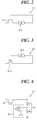
FIG. 2 is a circuit diagram illustrating an embodiment of a constant current source in a constant voltage supplying circuit for a circuit breaker according to an embodiment of the present invention; -
FIG. 3 is a circuit diagram illustrating an embodiment of a current adjusting circuit section in a constant voltage supplying circuit for a circuit breaker according to an embodiment of the present invention; -
FIG. 4 is a circuit diagram illustrating an embodiment of a feedback circuit section in a constant voltage supplying circuit for a circuit breaker according to an embodiment of the present invention; -
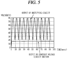
FIG. 5 is a waveform diagram illustrating waveforms of an input signal and an output signal in a constant voltage supplying circuit for a circuit breaker according to an embodiment of the present invention; -
FIG. 6 is waveform diagrams comparing a change of an output voltage of a constant voltage circuit according to a change of load resistance in the conventional art, with that in a constant voltage supplying circuit for a circuit breaker according to an embodiment of the present invention; and -
FIG. 7 is waveform diagrams comparing a current and voltage characteristic between a drain and a source of a first switching device in the conventional art, with that in a constant voltage supplying circuit for a circuit breaker according to an embodiment of the present invention. - Description will now be given in detail of preferred configurations of a constant voltage supplying circuit for a circuit breaker according to the present invention, with reference to the accompanying drawings.
- Firstly, a configuration of a constant voltage supplying circuit for a circuit breaker according to an embodiment the present invention will be explained with reference to
FIG. 1 . - The constant
voltage supplying circuit 10 for a circuit breaker according to an embodiment the present invention may be configured as a printed circuit board fixedly-installed in an enclosure of a low voltage circuit breaker such as a molded case circuit breaker or an earth leakage circuit breaker. - Referring to
FIG. 1 ,reference numeral 1 designates an alternating current electric power source (abbreviated as "AC power source" hereinafter), and may be configured as a three-phase commercial alternating current power source. - Referring to
FIG. 1 ,reference numeral 2 designates a rectifying circuit for supplying a direct current input voltage obtained by converting an alternating current into a direct current, to the constantvoltage supplying circuit 10. The rectifying circuit may be configured with a diode bridge circuit. In a case where theAC power source 1 is a three-phases AC power source, the rectifying circuit converts an alternating current for one of three phases into a direct current, thereby supplying the direct current. - The constant
voltage supplying circuit 10 comprises afirst switching device 11, a constantcurrent source 12, afeedback circuit section 13, aconstant voltage source 14, a currentadjusting circuit section 15, and a dividedvoltage resistor section 16. - The
first switching device 11 lowers (in other words "drops") a direct current input voltage supplied from the rectifyingcircuit 2, and supplies the direct current input voltage. - The
first switching device 11 can be configured as a pass transistor that provides a direct current input voltage after stepping down a voltage. The pass transistor is a switching device for controlling a high voltage and a large current. In the present invention, the pass transistor is used to utilize one of a high voltage control characteristic and a large current control characteristic, or both of the characteristics. - A voltage (VDS) between a drain and a source, and a current (IDS) between a drain and a source, of the pass transistor serving as the
first switching device 11 have a characteristic shown inFIG. 7 . Referring toFIG. 7 , as the voltage (VDS) between a drain and a source is increased, the characteristics of current (IDS) between a drain and a source shows a characteristics converging to a constant value. In the conventional art using a general transistor, the current (IDS) between a drain and a source has a comparatively large converged value of about 1A. On the other hand, in the present invention using the pass transistor, the current (IDS) between a drain and a source has a comparatively small converged value of about 1mA. - If an AC voltage of about 800V is applied to a circuit breaker as the AC
electric source 1, the voltage (VDS) between a drain and a source of thefirst switching device 11 may be lowered to about 10V. - The
first switching device 11 may have a source connected to an input terminal of the rectifyingcircuit 2, a drain connected to the currentadjusting circuit section 15, and a gate connected to thefeedback circuit section 13. - The constant
current source 12 is a means for supplying a constant current by being connected to thefirst switching device 11 in parallel. The constantcurrent source 12 supplies only a minimum current (Is) required by thefeedback circuit section 13 and theconstant voltage source 14. - As shown in
FIG. 2 , the constantcurrent source 12 may include a Depletion Metal Oxide Semiconductor (abbreviated as "DMOS" hereinafter) transistor 12-1, and a resistor 12-2 connected to the DMOS transistor 12-1. - A source of the DMOS transistor 12-1 may be connected to an input terminal of a direct current input voltage (Vin) supplied from the rectifying
circuit 2, and a drain of the DMOS transistor 12-1 may be connected to the resistor 12-2. - The DMOS transistor 12-1 is a switching device(a switching element) capable of enabling a current flow between a drain and a source by forming a current flowing channel when a gate voltage is not applied thereto, and capable of breaking current supply between the drain and the source by closing the current flowing channel when a gate voltage is applied thereto.
- Thus, the DMOS transistor 12-1 of the present invention serves to supply a current to the
feedback circuit section 13 by enabling a current flow between a drain and a source by forming a current flowing channel at an initial operation time of the constantvoltage supplying circuit 10. - Then, if an output voltage (Vf) of the
feedback circuit section 13 is formed to apply a gate voltage, the DMOS transistor 12-1 breaks the current flowing channel. As a result, a current path from the direct current input voltage (Vin) to the constantcurrent source 12 is disconnected, and only a current path of thefirst switching device 11 remains. - The resistor 12-2 may have one end connected to a drain of the DMOS transistor 12-1, and another end connected to a gate of the DMOS transistor 12-1 and the
feedback circuit section 13. - The resistor 12-2 limits current flow from the drain of the DMOS transistor 12-1 to the
feedback circuit section 13. - The
feedback circuit section 13 is commonly connected to an output terminals of thefirst switching device 11 and the constantcurrent source 12. - The
feedback circuit section 13 is connected to theconstant voltage source 14 and the currentadjusting circuit section 15. Further, thefeedback circuit section 13 is connected between a resistor (R1) and a resistor (R2) of the dividedvoltage resistor section 16. - If the switching device inside the current
adjusting circuit section 15 is turned on as a large amount of current flows through the currentadjusting circuit section 15, a voltage applied to the gate of thefirst switching device 11 is reduced to a value lower than a threshold voltage. As a result, thefirst switching device 11 is turned off, and an output current flows to an output terminal of the constantvoltage supplying circuit 10 is reduced. In this case, a current path from thefeedback circuit section 13 to the gate of thefirst switching device 11 is disconnected, and a current path from thefeedback circuit section 13 to the output terminal of the constantvoltage supplying circuit 10 through the currentadjusting circuit section 15 is created. - Once the
first switching device 11 is turned off, the switching device inside the currentadjusting circuit section 15 is turned off, because a small amount of current flows through the currentadjusting circuit section 15. And a current path from thefeedback circuit section 13 to the gate of thefirst switching device 11 is created, and a feedback voltage (Vf) of thefirst switching device 11 is re-applied to the gate of thefirst switching device 11. As a result, thefirst switching device 11 is turned on. If a large amount of output current flows to the output terminal of the constantvoltage supplying circuit 10, the switching device inside the currentadjusting circuit section 15 is turned on and thefirst switching device 11 is turned off. On the other hand, if a small amount of output current flows to the output terminal of the constantvoltage supplying circuit 10, the switching device inside the currentadjusting circuit section 15 is turned off and thefirst switching device 11 is turned on. With such a configuration, the amount of an output current flowing to the output terminal of the constantvoltage supplying circuit 10 may be maintained constantly. - As aforementioned, the
feedback circuit section 13 is used as a means to turn on or turn off thefirst switching device 11 according to an operation state of the currentadjusting circuit section 15. - Referring to
FIG. 4 , thefeedback circuit section 13 may include anoperational amplifier 13a. - In another embodiment, the
feedback circuit section 13 may be configured with a transistor (not shown). If thefeedback circuit section 13 is configured with a bipolar transistor, a collector of the bipolar transistor is connected to the constantcurrent source 12 and thefirst switching device 11, and a base of the bipolar transistor is connected to the resistor (R1) and the resistor (R2) of the dividedvoltage resistor section 16. And an emitter of the bipolar transistor is connected to theconstant voltage source 14. - The
constant voltage source 14 is connected to thefeedback circuit section 13, and supplies a reference voltage Vref as a constant voltage to thefeedback circuit section 13. - The
constant voltage source 14 may be configured with a Zener diode. - The current
adjusting circuit section 15 is connected to the output terminal of thefirst switching device 11, and adjusts an output current of the first switching device to be constant. - Referring to
FIG. 3 , the currentadjusting circuit section 15 includes a current limiting resistor 15-2, and a transistor 15-1 turned on or off according to the amount of a current flowing to the current limiting resistor 15-2. And the currentadjusting circuit section 15 is configured to turn off thefirst switching device 11 when the transistor 15-1 is turned on. - That is, if the transistor 15-1 is turned on as a large amount of current flows through the current limiting resistor 15-2, a voltage applied to the gate of the
first switching device 11 is reduced to a value less than a threshold voltage. As a result, thefirst switching device 11 is turned off. Thus, the amount of an output current flowing to the output terminal of the constantvoltage supplying circuit 10 is reduced. - When the
first switching device 11 is turned off, the transistor 15-1 is turned off since the amount of a current flowing through the currentadjusting circuit section 15 is reduced. And a current path from thefeedback circuit section 13 to the gate of thefirst switching device 11 is created, and the feedback voltage (Vf) of thefirst switching device 11 is re-applied to the gate of thefirst switching device 11. As a result, thefirst switching device 11 is turned on. If a large amount of output current flows to the output terminal of the constantvoltage supplying circuit 10, the transistor 15-1 of the currentadjusting circuit section 15 is turned on and thefirst switching device 11 is turned off. On the other hand, if a small amount of output current flows to the output terminal of the constantvoltage supplying circuit 10, the transistor 15-1 of the currentadjusting circuit section 15 is turned off and thefirst switching device 11 is turned on. With such a configuration, the amount of an output current flowing to the output terminal of the constantvoltage supplying circuit 10 may be maintained constantly. - The divided
voltage resistor section 16 is connected between an output terminal of the currentadjusting circuit section 15 and a ground, and includes a first resistor (R1) and a second resistor (R2). - The divided
voltage resistor section 16 provides a divided voltage of an output voltage (Vout) of the constantvoltage supplying circuit 10 to thefeedback circuit section 13, through a connection node between the first resistor (R1) and the second resistor (R2). - An operation of the constant voltage supplying circuit for a circuit breaker according to an embodiment of the present invention will be explained with reference to
figure 1 mainly, and other figures adjunctively. - Since an alternating current supplied from the
AC power source 1 is converted (rectified) into a direct current by the rectifyingcircuit 2 ofFIG. 1 , a direct current input voltage (Vin) is supplied to the constantvoltage supplying circuit 10. - At an initial time when the direct current input voltage (Vin) is supplied to the constant
voltage supplying circuit 10, thefirst switching device 11 is turned off, and the DMOS transistor 12-1 of the constantcurrent source 12 forms a current flowing channel. The DMOS transistor 12-1 supplies a current to thefeedback circuit section 13 by enabling a current flow between the drain and the source of the DMOS transistor 12-1. - Thus, the constant
current source 12 supplies a minimum current (Is) required by thefeedback circuit section 13 and theconstant voltage source 14. - The
feedback circuit section 13 applies, to thefirst switching device 11 and the currentadjusting circuit section 15, a reference voltage (Vref) of theconstant voltage source 14 and a voltage according to a ratio of the first resistor (R1) and the second resistor (R2) in the dividedvoltage resistor section 16. - That is, the voltage applied by the
feedback circuit section 13 may be obtained as follows.
- Here, the Vf designates an output voltage (applying voltage) of the
feedback circuit section 13, Vref designates a reference voltage provided from theconstant voltage source 14, and R1 and R2 designate a resistance of the first resistor and a resistance of the second resistor. - The Vref has a constant reference voltage provided from the
constant voltage source 14, and each of the R1 and R2 has a constant resistance value. Thus, the output voltage (applying voltage) of thefeedback circuit section 13 has a constant value. - Since the output voltage of the
feedback circuit section 13 is larger than a gate threshold voltage of thefirst switching device 11, thefirst switching device 11 is turned on as the output voltage is applied. - The direct current input voltage (Vin) is lowered to a desired value by the turned-on
first switching device 11, and is applied to the currentadjusting circuit section 15. - A final output voltage (Vout) of the constant
voltage supplying circuit 10 may be obtained as the followingformula 2, according to a relation among the output voltage (Vf) of thefeedback circuit section 13, a gate-source voltage (Vgs) of thefirst switching device 11, and a voltage drop (Vq) of the currentadjusting circuit section 15.
- Here, the output voltage (Vf) of the
feedback circuit section 13 is constant as aforementioned, the gate-source voltage (Vgs) of thefirst switching device 11 is constant if the direct current input voltage (Vin) is constant, and the voltage drop (Vq) of the currentadjusting circuit section 15 is constant. Thus, the final output voltage (Vout) of the constantvoltage supplying circuit 10 may be maintained constantly. - The transistor 15-1 of the current
adjusting circuit section 15 is turned on or turned off according to the amount of a current flowing through the currentadjusting circuit section 15, thereby constantly maintaining an output current of the constantvoltage supplying circuit 10. - For instance, as shown in
FIG. 5 , when a peak value of a direct current voltage supplied from the rectifyingcircuit 2 is 80(V), the final output voltage (Vout) of the constantvoltage supplying circuit 10 may be maintained constantly as about 15(V). - Referring to
FIG. 6 , in the conventional art, a final output voltage (Vout) of a constant voltage supplying circuit is increased as a load is increased. On the other hand, in the present invention, the final output voltage (Vout) of the constantvoltage supplying circuit 10 may be maintained constantly as a load is increased. - The final output voltage (Vout) of the constant
voltage supplying circuit 10 is supplied to an Zero Current Transformer (ZCT) 4, a leakage currentdetection circuit section 3, atrip switch 6 and a trip coil and aswitching mechanism 5, etc. ofFIG. 1 . - The
ZCT 4 is an element, which outputs a voltage signal corresponding to a leakage current which flows to a ground. - The leakage current
detection circuit section 3 compares a reference value (the reference value set for determination of a predetermined electric leakage) with respect to an output voltage of theZCT 4, with a value represented by an output voltage signal of theZCT 4. If the value of the output voltage of theZCT 4 is not less than the reference value, it is determined that electric leakage has occurred, and thetrip switch 6 is controlled to be switched to a closing position. Thetrip switch 6 may be configured with a switching device such as a transistor. - Then, as the
trip switch 6 is switched to the closing position, the final output voltage (Vout) of the constantvoltage supplying circuit 10 is supplied to the trip coil of the trip coil andswitching mechanism 5. As a result, the corresponding trip coils are magnetized. - As a trip mechanism such as an amateur (not shown) executes a trigger operation by the magnetization of the trip coil, the trip coil and
switching mechanism 5 drive a movable contact arm (not shown) to a position where the movable contact arm is separated from a stationary contact arm. As a result, a circuit is broken, and the circuit, electric load (utilization equipment) connected to the circuit, etc. are protected from electric leakage. - The constant voltage supplying circuit for a circuit breaker according to the present invention may have the following advantages.
- Firstly, since the constant voltage supplying circuit for a circuit breaker according to the present invention comprises the constant current source instead of a resistor for voltage drop is installed at an input terminal in the conventional art, heat emission, a large occupation area and a high price due to the resistor may be solved.
- Secondly, in the constant voltage supplying circuit for a circuit breaker according to the present invention, a constant DC voltage may be provided as an input voltage is lowered by the constant current source, the pass transistor, and the feedback circuit section.
- Thirdly, the constant voltage supplying circuit for a circuit breaker according to the present invention comprises the current adjusting circuit section, so a limited current is supplied until an output voltage of each of the feedback circuit section becomes stabilized. Further, unnecessary current consumption is limited if the output voltage of the feedback circuit section becomes stable to a level of a final output voltage of the constant voltage supplying circuit. This may allow an output current and an output voltage of the constant voltage supplying circuit to be maintained constantly, regardless of a change of an output side load.
- Fourthly, in the constant voltage supplying circuit for a circuit breaker according to the present invention, a standby power may be reduced due to small current consumption.
- As the present features may be embodied in several forms without departing from the characteristics thereof, it should also be understood that the above-described embodiments are not limited by any of the details of the foregoing description, unless otherwise specified, but rather should be construed broadly within its scope as defined in the appended claims, and therefore all changes and modifications that fall within the metes and bounds of the claims, or equivalents of such metes and bounds are therefore intended to be embraced by the appended claims.
Claims (7)
- A constant voltage supplying circuit for a circuit breaker, which receives a direct current input voltage obtained by converting an alternating current to a direct current from a rectifying circuit, characterized in that the constant voltage supplying circuit comprising:a first switching device (11) configured to supply the direct current input voltage after stepping down a voltage;a constant current source (12) connected to the first switching device (11) in parallel, and configured to supply a constant current;a feedback circuit section (13) commonly connected to the first switching device (11) and output terminal of the constant current source (12);a constant voltage source (14) connected to the feedback circuit section (13), and configured to supply a constant voltage;a current adjusting circuit section (15) connected to the output terminal of the first switching device (11), and configured to adjust an output current of the first switching device (11); anda divided voltage resistor section (16) connected to an output terminal of the current adjusting circuit section (15) and a ground, including a first resistor (R1) and a second resistor (R2), and configured to provide a divided voltage of an output voltage of the constant voltage supplying circuit, to the feedback circuit section (13), through a connection node between the first resistor (R1) and the second resistor (R2).
- The constant voltage supplying circuit for a circuit breaker of claim 1, wherein the constant current source (12) comprises a Depletion Metal Oxide Semiconductor (DMOS) transistor (12-1), and a resistor (12-2) connected to the DMOS transistor (12-1).
- The constant voltage supplying circuit for a circuit breaker of claim 1 or claim 2, wherein the feedback circuit section (13) comprises an operational amplifier (13a).
- The constant voltage supplying circuit for a circuit breaker of any one of claims 1-3, wherein the feedback circuit section (13) comprises a transistor.
- The constant voltage supplying circuit for a circuit breaker of any one of claims 1-4, wherein the constant voltage source (14) comprises a Zener diode.
- The constant voltage supplying circuit for a circuit breaker of any one of claims 1-5, wherein the current adjusting circuit section (15) comprises:a current limiting resistor (15-2); anda transistor (15-1) that is turned on or off according to an amount of a current flows through the current limiting resistor (15-2), andwherein the current adjusting circuit section (15) is configured to turn off the first switching device (11) when the transistor (15-1) is turned on.
- The constant voltage supplying circuit for a circuit breaker of any one of claims 1-6, wherein the first switching device (11) is configured with a pass transistor that provides a direct current input voltage after stepping down a voltage.
Applications Claiming Priority (1)
| Application Number | Priority Date | Filing Date | Title |
|---|---|---|---|
| KR1020150094127A KR101748726B1 (en) | 2015-07-01 | 2015-07-01 | Constant voltage supplying circuit for circuit breaker |
Publications (1)
| Publication Number | Publication Date |
|---|---|
| EP3112973A1 true EP3112973A1 (en) | 2017-01-04 |
Family
ID=55952963
Family Applications (1)
| Application Number | Title | Priority Date | Filing Date |
|---|---|---|---|
| EP16166837.1A Withdrawn EP3112973A1 (en) | 2015-07-01 | 2016-04-25 | Constant voltage supplying circuit for circuit breaker |
Country Status (5)
| Country | Link |
|---|---|
| US (1) | US10176951B2 (en) |
| EP (1) | EP3112973A1 (en) |
| JP (1) | JP6254641B2 (en) |
| KR (1) | KR101748726B1 (en) |
| CN (1) | CN106329960B (en) |
Cited By (2)
| Publication number | Priority date | Publication date | Assignee | Title |
|---|---|---|---|---|
| GB2563839A (en) * | 2017-06-26 | 2019-01-02 | Ge Aviation Systems Group Ltd | System and method for limiting currents in a power distribution system |
| CN110768510A (en) * | 2019-09-30 | 2020-02-07 | 上海芃矽半导体技术有限公司 | Control circuit and method and power converter |
Families Citing this family (1)
| Publication number | Priority date | Publication date | Assignee | Title |
|---|---|---|---|---|
| JP7024137B2 (en) | 2019-02-22 | 2022-02-22 | アルプスアルパイン株式会社 | DC voltage conversion circuit and switching power supply |
Citations (4)
| Publication number | Priority date | Publication date | Assignee | Title |
|---|---|---|---|---|
| US4833563A (en) * | 1988-04-01 | 1989-05-23 | General Electric Company | Molded case circuit breaker actuator-accessory module |
| US6233128B1 (en) * | 1999-03-29 | 2001-05-15 | George A. Spencer | Data retention in a circuit breaker |
| KR20050040718A (en) | 2003-10-29 | 2005-05-03 | 후지 덴키 기기세이교 가부시끼가이샤 | Dc power source circuit and ground-fault circuit interrupter using dc power source circuit |
| KR101001768B1 (en) | 2008-12-31 | 2010-12-15 | 엘에스산전 주식회사 | Constant voltage circuit |
Family Cites Families (11)
| Publication number | Priority date | Publication date | Assignee | Title |
|---|---|---|---|---|
| JP4772980B2 (en) | 2001-04-19 | 2011-09-14 | セイコーインスツル株式会社 | Voltage regulator |
| JP3539940B2 (en) * | 2001-07-30 | 2004-07-07 | 沖電気工業株式会社 | Voltage regulator |
| JP4774247B2 (en) | 2005-07-21 | 2011-09-14 | Okiセミコンダクタ株式会社 | Voltage regulator |
| KR100714823B1 (en) | 2005-09-09 | 2007-05-07 | 주식회사 엑셀반도체 | Mutiple valued SRAM |
| JP4961739B2 (en) | 2005-12-27 | 2012-06-27 | ミツミ電機株式会社 | Power supply circuit and starting method thereof |
| JP4855841B2 (en) | 2006-06-14 | 2012-01-18 | 株式会社リコー | Constant voltage circuit and output voltage control method thereof |
| KR101214103B1 (en) | 2011-06-07 | 2012-12-20 | 에코엘이디(주) | Lighting unit for emergency |
| KR101422924B1 (en) | 2012-10-18 | 2014-08-13 | 삼성전기주식회사 | Low drop-out regulator |
| CN104995576A (en) * | 2013-07-25 | 2015-10-21 | 柏恩氏股份有限公司 | A non-isolated ac to dc power device |
| JP6268485B2 (en) * | 2014-07-14 | 2018-01-31 | 富士電機機器制御株式会社 | Earth leakage breaker |
| EP2980660B1 (en) * | 2014-07-28 | 2016-11-23 | Pepperl & Fuchs GmbH | Method and device for monitoring and switching a load circuit |
-
2015
- 2015-07-01 KR KR1020150094127A patent/KR101748726B1/en active IP Right Grant
-
2016
- 2016-04-21 US US15/135,446 patent/US10176951B2/en active Active
- 2016-04-25 EP EP16166837.1A patent/EP3112973A1/en not_active Withdrawn
- 2016-05-16 JP JP2016097698A patent/JP6254641B2/en active Active
- 2016-06-20 CN CN201610446199.XA patent/CN106329960B/en active Active
Patent Citations (4)
| Publication number | Priority date | Publication date | Assignee | Title |
|---|---|---|---|---|
| US4833563A (en) * | 1988-04-01 | 1989-05-23 | General Electric Company | Molded case circuit breaker actuator-accessory module |
| US6233128B1 (en) * | 1999-03-29 | 2001-05-15 | George A. Spencer | Data retention in a circuit breaker |
| KR20050040718A (en) | 2003-10-29 | 2005-05-03 | 후지 덴키 기기세이교 가부시끼가이샤 | Dc power source circuit and ground-fault circuit interrupter using dc power source circuit |
| KR101001768B1 (en) | 2008-12-31 | 2010-12-15 | 엘에스산전 주식회사 | Constant voltage circuit |
Cited By (4)
| Publication number | Priority date | Publication date | Assignee | Title |
|---|---|---|---|---|
| GB2563839A (en) * | 2017-06-26 | 2019-01-02 | Ge Aviation Systems Group Ltd | System and method for limiting currents in a power distribution system |
| GB2563839B (en) * | 2017-06-26 | 2020-11-18 | Ge Aviat Systems Ltd | System and method for limiting currents in a power distribution system |
| US10972087B2 (en) | 2017-06-26 | 2021-04-06 | Ge Aviation Systems Limited | System and method for limting currents in a power distribution system |
| CN110768510A (en) * | 2019-09-30 | 2020-02-07 | 上海芃矽半导体技术有限公司 | Control circuit and method and power converter |
Also Published As
| Publication number | Publication date |
|---|---|
| CN106329960A (en) | 2017-01-11 |
| CN106329960B (en) | 2019-01-01 |
| KR20170004161A (en) | 2017-01-11 |
| US10176951B2 (en) | 2019-01-08 |
| JP6254641B2 (en) | 2017-12-27 |
| KR101748726B1 (en) | 2017-06-19 |
| US20170004944A1 (en) | 2017-01-05 |
| JP2017016641A (en) | 2017-01-19 |
Similar Documents
| Publication | Publication Date | Title |
|---|---|---|
| CN107786093B (en) | Method for regulating a supply voltage | |
| CN101369773B (en) | Method, device and system for start-up time reduction in switching regulators | |
| EP2093873B1 (en) | AC-DC converter | |
| US10516338B2 (en) | Voltage converter controller, voltage converter and method for operating a voltage converter | |
| US8243478B2 (en) | Method and apparatus for limiting maximum output power of a power converter | |
| KR101677729B1 (en) | Switch control device, power supply device comprising the same, and switch control method | |
| KR101247801B1 (en) | Switching mode power supply | |
| US8987999B2 (en) | LED driver | |
| US8891259B2 (en) | Control circuit and method for audible noise suppression in a power converter | |
| KR101489962B1 (en) | Power converter, switching control device thereof and driving method thereof | |
| US8964412B2 (en) | Split current mirror line sensing | |
| CN111064356B (en) | Power supply circuit capable of improving power factor | |
| US10176951B2 (en) | Constant voltage supplying circuit for circuit breaker | |
| US7369391B2 (en) | Drive circuit of direct-current voltage-driven magnetic contactor and power converter | |
| US9502983B2 (en) | Power supply device capable of varying switching frequency according to load condition | |
| CN106899218B (en) | For using the accessory power supply of the switch mode power controller of relay system rule | |
| KR101367954B1 (en) | Switching mode power supply and switching controlling circuit thereof | |
| US10615681B2 (en) | Switching power supply circuit | |
| CN203490577U (en) | Series transfer regulator and regulating circuit | |
| US9537396B2 (en) | Power switch control by adjusting the base current of a bipolar transistor | |
| US20070291517A1 (en) | Power supply circuit with positive feedback circuit | |
| WO2004057744A1 (en) | Self-oscillating power supply | |
| CN104093256B (en) | Led drive circuit and led driving method | |
| CN104093256A (en) | LED drive circuit and LED drive method |
Legal Events
| Date | Code | Title | Description |
|---|---|---|---|
| PUAI | Public reference made under article 153(3) epc to a published international application that has entered the european phase |
Free format text: ORIGINAL CODE: 0009012 |
|
| STAA | Information on the status of an ep patent application or granted ep patent |
Free format text: STATUS: THE APPLICATION HAS BEEN PUBLISHED |
|
| AK | Designated contracting states |
Kind code of ref document: A1 Designated state(s): AL AT BE BG CH CY CZ DE DK EE ES FI FR GB GR HR HU IE IS IT LI LT LU LV MC MK MT NL NO PL PT RO RS SE SI SK SM TR |
|
| AX | Request for extension of the european patent |
Extension state: BA ME |
|
| STAA | Information on the status of an ep patent application or granted ep patent |
Free format text: STATUS: REQUEST FOR EXAMINATION WAS MADE |
|
| 17P | Request for examination filed |
Effective date: 20170630 |
|
| RBV | Designated contracting states (corrected) |
Designated state(s): AL AT BE BG CH CY CZ DE DK EE ES FI FR GB GR HR HU IE IS IT LI LT LU LV MC MK MT NL NO PL PT RO RS SE SI SK SM TR |
|
| STAA | Information on the status of an ep patent application or granted ep patent |
Free format text: STATUS: EXAMINATION IS IN PROGRESS |
|
| 17Q | First examination report despatched |
Effective date: 20180712 |
|
| STAA | Information on the status of an ep patent application or granted ep patent |
Free format text: STATUS: EXAMINATION IS IN PROGRESS |
|
| STAA | Information on the status of an ep patent application or granted ep patent |
Free format text: STATUS: EXAMINATION IS IN PROGRESS |
|
| STAA | Information on the status of an ep patent application or granted ep patent |
Free format text: STATUS: THE APPLICATION IS DEEMED TO BE WITHDRAWN |
|
| 18D | Application deemed to be withdrawn |
Effective date: 20230620 |