EP3112316A1 - Method for manufacturing a transistor devices comprising multiple nanowire channels, and cmos devices - Google Patents
Method for manufacturing a transistor devices comprising multiple nanowire channels, and cmos devices Download PDFInfo
- Publication number
- EP3112316A1 EP3112316A1 EP15174968.6A EP15174968A EP3112316A1 EP 3112316 A1 EP3112316 A1 EP 3112316A1 EP 15174968 A EP15174968 A EP 15174968A EP 3112316 A1 EP3112316 A1 EP 3112316A1
- Authority
- EP
- European Patent Office
- Prior art keywords
- layer
- germanium
- stack
- silicon germanium
- silicon
- Prior art date
- Legal status (The legal status is an assumption and is not a legal conclusion. Google has not performed a legal analysis and makes no representation as to the accuracy of the status listed.)
- Granted
Links
Images

Classifications
-
- B—PERFORMING OPERATIONS; TRANSPORTING
- B82—NANOTECHNOLOGY
- B82Y—SPECIFIC USES OR APPLICATIONS OF NANOSTRUCTURES; MEASUREMENT OR ANALYSIS OF NANOSTRUCTURES; MANUFACTURE OR TREATMENT OF NANOSTRUCTURES
- B82Y10/00—Nanotechnology for information processing, storage or transmission, e.g. quantum computing or single electron logic
-
- B—PERFORMING OPERATIONS; TRANSPORTING
- B82—NANOTECHNOLOGY
- B82Y—SPECIFIC USES OR APPLICATIONS OF NANOSTRUCTURES; MEASUREMENT OR ANALYSIS OF NANOSTRUCTURES; MANUFACTURE OR TREATMENT OF NANOSTRUCTURES
- B82Y40/00—Manufacture or treatment of nanostructures
-
- H—ELECTRICITY
- H10—SEMICONDUCTOR DEVICES; ELECTRIC SOLID-STATE DEVICES NOT OTHERWISE PROVIDED FOR
- H10D—INORGANIC ELECTRIC SEMICONDUCTOR DEVICES
- H10D30/00—Field-effect transistors [FET]
- H10D30/01—Manufacture or treatment
- H10D30/014—Manufacture or treatment of FETs having zero-dimensional [0D] or one-dimensional [1D] channels, e.g. quantum wire FETs, single-electron transistors [SET] or Coulomb blockade transistors
-
- H—ELECTRICITY
- H10—SEMICONDUCTOR DEVICES; ELECTRIC SOLID-STATE DEVICES NOT OTHERWISE PROVIDED FOR
- H10D—INORGANIC ELECTRIC SEMICONDUCTOR DEVICES
- H10D30/00—Field-effect transistors [FET]
- H10D30/01—Manufacture or treatment
- H10D30/021—Manufacture or treatment of FETs having insulated gates [IGFET]
- H10D30/025—Manufacture or treatment of FETs having insulated gates [IGFET] of vertical IGFETs
-
- H—ELECTRICITY
- H10—SEMICONDUCTOR DEVICES; ELECTRIC SOLID-STATE DEVICES NOT OTHERWISE PROVIDED FOR
- H10D—INORGANIC ELECTRIC SEMICONDUCTOR DEVICES
- H10D30/00—Field-effect transistors [FET]
- H10D30/40—FETs having zero-dimensional [0D], one-dimensional [1D] or two-dimensional [2D] charge carrier gas channels
- H10D30/43—FETs having zero-dimensional [0D], one-dimensional [1D] or two-dimensional [2D] charge carrier gas channels having one-dimensional [1D] charge carrier gas channels, e.g. quantum wire FETs or transistors having 1D quantum-confined channels
-
- H—ELECTRICITY
- H10—SEMICONDUCTOR DEVICES; ELECTRIC SOLID-STATE DEVICES NOT OTHERWISE PROVIDED FOR
- H10D—INORGANIC ELECTRIC SEMICONDUCTOR DEVICES
- H10D30/00—Field-effect transistors [FET]
- H10D30/60—Insulated-gate field-effect transistors [IGFET]
- H10D30/63—Vertical IGFETs
-
- H—ELECTRICITY
- H10—SEMICONDUCTOR DEVICES; ELECTRIC SOLID-STATE DEVICES NOT OTHERWISE PROVIDED FOR
- H10D—INORGANIC ELECTRIC SEMICONDUCTOR DEVICES
- H10D30/00—Field-effect transistors [FET]
- H10D30/60—Insulated-gate field-effect transistors [IGFET]
- H10D30/67—Thin-film transistors [TFT]
- H10D30/6729—Thin-film transistors [TFT] characterised by the electrodes
- H10D30/673—Thin-film transistors [TFT] characterised by the electrodes characterised by the shapes, relative sizes or dispositions of the gate electrodes
- H10D30/6735—Thin-film transistors [TFT] characterised by the electrodes characterised by the shapes, relative sizes or dispositions of the gate electrodes having gates fully surrounding the channels, e.g. gate-all-around
-
- H—ELECTRICITY
- H10—SEMICONDUCTOR DEVICES; ELECTRIC SOLID-STATE DEVICES NOT OTHERWISE PROVIDED FOR
- H10D—INORGANIC ELECTRIC SEMICONDUCTOR DEVICES
- H10D30/00—Field-effect transistors [FET]
- H10D30/60—Insulated-gate field-effect transistors [IGFET]
- H10D30/67—Thin-film transistors [TFT]
- H10D30/6757—Thin-film transistors [TFT] characterised by the structure of the channel, e.g. transverse or longitudinal shape or doping profile
-
- H—ELECTRICITY
- H10—SEMICONDUCTOR DEVICES; ELECTRIC SOLID-STATE DEVICES NOT OTHERWISE PROVIDED FOR
- H10D—INORGANIC ELECTRIC SEMICONDUCTOR DEVICES
- H10D30/00—Field-effect transistors [FET]
- H10D30/60—Insulated-gate field-effect transistors [IGFET]
- H10D30/791—Arrangements for exerting mechanical stress on the crystal lattice of the channel regions
- H10D30/798—Arrangements for exerting mechanical stress on the crystal lattice of the channel regions being provided in or under the channel regions
-
- H—ELECTRICITY
- H10—SEMICONDUCTOR DEVICES; ELECTRIC SOLID-STATE DEVICES NOT OTHERWISE PROVIDED FOR
- H10D—INORGANIC ELECTRIC SEMICONDUCTOR DEVICES
- H10D62/00—Semiconductor bodies, or regions thereof, of devices having potential barriers
- H10D62/10—Shapes, relative sizes or dispositions of the regions of the semiconductor bodies; Shapes of the semiconductor bodies
- H10D62/117—Shapes of semiconductor bodies
- H10D62/118—Nanostructure semiconductor bodies
- H10D62/119—Nanowire, nanosheet or nanotube semiconductor bodies
- H10D62/121—Nanowire, nanosheet or nanotube semiconductor bodies oriented parallel to substrates
-
- H—ELECTRICITY
- H10—SEMICONDUCTOR DEVICES; ELECTRIC SOLID-STATE DEVICES NOT OTHERWISE PROVIDED FOR
- H10D—INORGANIC ELECTRIC SEMICONDUCTOR DEVICES
- H10D62/00—Semiconductor bodies, or regions thereof, of devices having potential barriers
- H10D62/10—Shapes, relative sizes or dispositions of the regions of the semiconductor bodies; Shapes of the semiconductor bodies
- H10D62/117—Shapes of semiconductor bodies
- H10D62/118—Nanostructure semiconductor bodies
- H10D62/119—Nanowire, nanosheet or nanotube semiconductor bodies
- H10D62/122—Nanowire, nanosheet or nanotube semiconductor bodies oriented at angles to substrates, e.g. perpendicular to substrates
-
- H—ELECTRICITY
- H10—SEMICONDUCTOR DEVICES; ELECTRIC SOLID-STATE DEVICES NOT OTHERWISE PROVIDED FOR
- H10D—INORGANIC ELECTRIC SEMICONDUCTOR DEVICES
- H10D62/00—Semiconductor bodies, or regions thereof, of devices having potential barriers
- H10D62/80—Semiconductor bodies, or regions thereof, of devices having potential barriers characterised by the materials
- H10D62/83—Semiconductor bodies, or regions thereof, of devices having potential barriers characterised by the materials being Group IV materials, e.g. B-doped Si or undoped Ge
-
- H—ELECTRICITY
- H10—SEMICONDUCTOR DEVICES; ELECTRIC SOLID-STATE DEVICES NOT OTHERWISE PROVIDED FOR
- H10D—INORGANIC ELECTRIC SEMICONDUCTOR DEVICES
- H10D64/00—Electrodes of devices having potential barriers
- H10D64/20—Electrodes characterised by their shapes, relative sizes or dispositions
- H10D64/27—Electrodes not carrying the current to be rectified, amplified, oscillated or switched, e.g. gates
- H10D64/311—Gate electrodes for field-effect devices
- H10D64/411—Gate electrodes for field-effect devices for FETs
- H10D64/511—Gate electrodes for field-effect devices for FETs for IGFETs
- H10D64/512—Disposition of the gate electrodes, e.g. buried gates
-
- H—ELECTRICITY
- H10—SEMICONDUCTOR DEVICES; ELECTRIC SOLID-STATE DEVICES NOT OTHERWISE PROVIDED FOR
- H10D—INORGANIC ELECTRIC SEMICONDUCTOR DEVICES
- H10D84/00—Integrated devices formed in or on semiconductor substrates that comprise only semiconducting layers, e.g. on Si wafers or on GaAs-on-Si wafers
- H10D84/01—Manufacture or treatment
- H10D84/0123—Integrating together multiple components covered by H10D12/00 or H10D30/00, e.g. integrating multiple IGBTs
- H10D84/0126—Integrating together multiple components covered by H10D12/00 or H10D30/00, e.g. integrating multiple IGBTs the components including insulated gates, e.g. IGFETs
- H10D84/0165—Integrating together multiple components covered by H10D12/00 or H10D30/00, e.g. integrating multiple IGBTs the components including insulated gates, e.g. IGFETs the components including complementary IGFETs, e.g. CMOS devices
- H10D84/0167—Manufacturing their channels
-
- H—ELECTRICITY
- H10—SEMICONDUCTOR DEVICES; ELECTRIC SOLID-STATE DEVICES NOT OTHERWISE PROVIDED FOR
- H10D—INORGANIC ELECTRIC SEMICONDUCTOR DEVICES
- H10D84/00—Integrated devices formed in or on semiconductor substrates that comprise only semiconducting layers, e.g. on Si wafers or on GaAs-on-Si wafers
- H10D84/01—Manufacture or treatment
- H10D84/02—Manufacture or treatment characterised by using material-based technologies
- H10D84/03—Manufacture or treatment characterised by using material-based technologies using Group IV technology, e.g. silicon technology or silicon-carbide [SiC] technology
- H10D84/038—Manufacture or treatment characterised by using material-based technologies using Group IV technology, e.g. silicon technology or silicon-carbide [SiC] technology using silicon technology, e.g. SiGe
-
- H—ELECTRICITY
- H10—SEMICONDUCTOR DEVICES; ELECTRIC SOLID-STATE DEVICES NOT OTHERWISE PROVIDED FOR
- H10D—INORGANIC ELECTRIC SEMICONDUCTOR DEVICES
- H10D84/00—Integrated devices formed in or on semiconductor substrates that comprise only semiconducting layers, e.g. on Si wafers or on GaAs-on-Si wafers
- H10D84/80—Integrated devices formed in or on semiconductor substrates that comprise only semiconducting layers, e.g. on Si wafers or on GaAs-on-Si wafers characterised by the integration of at least one component covered by groups H10D12/00 or H10D30/00, e.g. integration of IGFETs
- H10D84/82—Integrated devices formed in or on semiconductor substrates that comprise only semiconducting layers, e.g. on Si wafers or on GaAs-on-Si wafers characterised by the integration of at least one component covered by groups H10D12/00 or H10D30/00, e.g. integration of IGFETs of only field-effect components
- H10D84/83—Integrated devices formed in or on semiconductor substrates that comprise only semiconducting layers, e.g. on Si wafers or on GaAs-on-Si wafers characterised by the integration of at least one component covered by groups H10D12/00 or H10D30/00, e.g. integration of IGFETs of only field-effect components of only insulated-gate FETs [IGFET]
- H10D84/85—Complementary IGFETs, e.g. CMOS
-
- H—ELECTRICITY
- H10—SEMICONDUCTOR DEVICES; ELECTRIC SOLID-STATE DEVICES NOT OTHERWISE PROVIDED FOR
- H10P—GENERIC PROCESSES OR APPARATUS FOR THE MANUFACTURE OR TREATMENT OF DEVICES COVERED BY CLASS H10
- H10P50/00—Etching of wafers, substrates or parts of devices
- H10P50/20—Dry etching; Plasma etching; Reactive-ion etching
- H10P50/24—Dry etching; Plasma etching; Reactive-ion etching of semiconductor materials
- H10P50/242—Dry etching; Plasma etching; Reactive-ion etching of semiconductor materials of Group IV materials
-
- H—ELECTRICITY
- H10—SEMICONDUCTOR DEVICES; ELECTRIC SOLID-STATE DEVICES NOT OTHERWISE PROVIDED FOR
- H10D—INORGANIC ELECTRIC SEMICONDUCTOR DEVICES
- H10D84/00—Integrated devices formed in or on semiconductor substrates that comprise only semiconducting layers, e.g. on Si wafers or on GaAs-on-Si wafers
- H10D84/01—Manufacture or treatment
- H10D84/0123—Integrating together multiple components covered by H10D12/00 or H10D30/00, e.g. integrating multiple IGBTs
- H10D84/0126—Integrating together multiple components covered by H10D12/00 or H10D30/00, e.g. integrating multiple IGBTs the components including insulated gates, e.g. IGFETs
- H10D84/0128—Manufacturing their channels
Definitions
- the present disclosure relates to transistor devices comprising multiple nanowire channels, and associated CMOS devices.
- CMOS technology is being complemented or replaced by technology based on other material systems.
- Gate-all-around devices on nanowires wherein gates are provided which completely surround nanowire channel structures of a transistor, are required to improve the short channel control of advanced node devices in order to allow continued gate length scaling.
- CMOS processing is to combine different semiconductor materials as channel materials on the same substrate, for instance for use as NMOS and PMOS devices respectively.
- NMOS and PMOS nanowire devices are disclosed wherein both NMOS and PMOS devices comprise a vertical stack of nanowires to achieve a greater current carrying capability (e.g. larger drive currents) for a given device footprint over a substrate.
- the NMOS nanowire transistor comprises group III-V semiconductor material, e.g. GaAs
- the PMOS nanowire comprises group IV semiconductor material, e.g. Germanium.
- both NMOS and PMOS device fabrication comprises the growth of a single stack of layers wherein alternatingly a layer of a group IV semiconductor material and a layer of a group III-V semiconductor material are grown on top of each other. In an NMOS region, the group IV semiconductor layer is then selectively removed, while in a PMOS region the group III-V semiconductor layer is selectively removed.
- a method for manufacturing a transistor device comprising multiple nanowire channels arranged above one another in a vertical stack, the method comprising
- the method comprises
- the first selective removal step and the second selective removal step may be independent steps or may comprise a single step.
- a single step is performed, e.g. a single etch step, this is such that the first layer is removed first at a much higher speed than the second layer.
- the removal of the second layer can proceed in an accelerated manner as its upper or lower surface is then exposed to the etching substance.
- the method may further comprise performing a recess etch creating recesses in between STI structures in a substrate, and growing the layer stack within said recesses.
- the layer stack can be grown on a blanked wafer, and can then be patterned into fin-type structures, protruding from the substrate.
- the first layer has a relatively low germanium concentration
- the second layer has a relatively average silicon germanium concentration
- the third layer has a relatively high germanium concentration
- selectively removing the first layer and selectively removing the second layer comprises etching in a wet alkaline solution.
- the first layer can be a silicon layer
- the second layer can be a silicon germanium layer
- the third layer can be a germanium layer
- selectively removing the first layer and selectively removing the second layer comprises etching in a wet alkaline solution.
- the wet alkaline solution can for instance be or comprise TMAH, NaOH, KOH, EDP or NH4OH.
- the germanium layer then remains as a nanowire channel.
- the first layer has a relatively high germanium concentration
- the second layer has a relatively average germanium concentration
- the third layer has a relatively low germanium concentration
- selectively removing the first layer and selectively removing the second layer comprises a HCl gas phase etch, a CF4 dry etch or etch with a APM.
- the first layer can be a germanium layer
- the second layer can be a silicon germanium layer
- the third layer can be a silicon layer
- selectively removing the first layer and selectively removing the second layer can comprise a HCl gas phase etch, a CF4 dry etch or etch with a APM (Ammonia and hydrogen Peroxide Mixture).
- the silicon layer then remains as a nanowire channel.
- the first layer has a relatively high germanium concentration
- the second layer has a relatively low germanium concentration
- the third layer has a relatively average germanium concentration
- selectively removing the first layer comprises etching with O3/deionised water (DIW), O3HCl or O3/NH4OH
- selectively removing the second layer comprises etching in a wet alkaline solution.
- the first layer can be a germanium layer
- the second layer can be a silicon layer
- the third layer can be a silicon germanium layer
- selectively removing the first layer can comprise etching with O3/deionised water (DIW) and selectively removing the second layer can comprise etching in a wet alkaline solution (for examples, see embodiments of the first type).
- DIW O3/deionised water
- the silicon germanium layer then remains as a nanowire channel.
- the method comprises
- the first, second and third channel regions preferably correspond respectively to a high performance PMOS (Germanium nanowire channels), an NMOS (silicon naowire channels) and a PMOS (SiGe nanowire channels) nanowire transistor.
- the method comprises providing one or more gate structures provided all around the nanowire channels.
- the predetermined order of the relatively low germanium concentration silicon germanium layer, the relatively average germanium concentration silicon germanium layer and the relatively high germanium concentration silicon germanium layer is: relatively high germanium concentration silicon germanium layer - relatively low germanium concentration silicon germanium layer - relatively average germanium concentration silicon germanium.
- the predetermined order of a silicon layer, a silicon germanium layer and a germanium layer is: germanium - silicon - silicon germanium from lower layer to upper layer.
- the predetermined order of the relatively low germanium concentration silicon germanium layer, the relatively average germanium concentration silicon germanium layer and the relatively high germanium concentration silicon germanium layer is : relatively high germanium concentration silicon germanium layer - relatively average germanium concentration silicon germanium layer - relatively low germanium concentration silicon germanium layer from lower layer to upper layer.
- the predetermined order of a silicon layer, a silicon germanium layer and a germanium layer is: germanium - silicon germanium - silicon from lower layer to upper layer.
- the substrate is a strain relaxed buffer (SRB) SiGe substrate or a silicon substrate
- the Germanium layers of the basic layer stacks are grown with compressive stress
- the Silicon layers of the basic layer stacks are grown with tensile stress
- the SiGe layers of the basic layer stacks are grown such that they are relaxed or strained.
- growing the layer stack comprises subsequently growing a plurality of basic layer stacks directly on top of one another.
- the basic layer stacks are identical in constitution.
- a single layer stack is applied over a main surface of the substrate, and is then patterned. After patterning the layer stack can still be present in the first region, or for instance in the first region, second region and third region.
- a CMOS device comprising at least three types of transistor devices arranged in a substrate, wherein each type of transistor device comprises multiple nanowire channels arranged above one another in a vertical stack, wherein the nanowire channels of the same type of transistor device comprise the same materials, and wherein a first type of transistor device comprises Si nanowire channels, a second type of transistor device comprises Ge nanowire channels, and a third type of transistor device comprises SiGe nanowire channels.
- the nanowire channels of the different types of transistor devices are arranged at different, non-overlapping height ranges above the substrate.
- the nanowire channels of different types of transistor devices may be off-set in the height direction.
- the removal of a SiGe layer with a Ge concentration x with respect to a (preferably interfacing) SiGe layer with a Ge concentration y, with y>x is performed in an alkaline solution as described before, at temperatures within the range of 70 to 90oC.
- all oxidizing species are removed from the etching solution (i.e. they are not present in the etching solution), as for instance dissolved oxygen and traces of hydrogen peroxide. This will strongly limit the selective etch to the low concentration Ge layer only. It was found that if the oxidizing species are present, at these high temperatures, an isotropic or less selective etch process occurs.
- Gate-all-around devices on nanowires are required to improve the short channel control of advanced node devices in order to allow continued gate length scaling.
- a method for fabricating tensile-strained Si wires (typically used for NMOS), strained or unstrained SiGe wires (typically used for PMOS) and compressively-strained Ge wires (typically used for High Performance (HP) PMOS) on a common substrate.
- tensile-strained Si wires typically used for NMOS
- strained or unstrained SiGe wires typically used for PMOS
- compressively-strained Ge wires typically used for High Performance (HP) PMOS
- a method for fabricating tensile-strained SiGe wires (typically used for NMOS), strained or unstrained SiGe wires (typically used for PMOS) and compressive-strained SiGe wires (typically used for High Performance (HP) PMOS) on a common substrate.
- the tensile-strained, compressive strained and unstrained SiGe wires typically have a different germanium concentration.
- a layer stack is grown on a substrate in at least a first channel region, the layer stack comprising a plurality of basic layer stacks, the basic layer stack comprising a first silicon germanium layer, a second silicon germanium layer and a third silicon germanium layer in a predetermined order, the first, second and third silicon germanium layers having substantially different germanium concentrations.
- one of the three silicon germanium layers has a relatively low germanium concentration
- another of the three silicon germanium layers has a relatively average silicon germanium concentration
- another of the three silicon germanium layers has a relatively high germanium concentration.
- the relatively low germanium concentration is preferably within the closed range of 0 to 50%.
- the relatively average germanium concentration is preferably within the closed range of 25 to 75 %.
- the relatively high germanium concentration is preferably within the closed range of 50 to 100%.
- the relative difference in germanium concentration between any two of the three silicon germanium layers is larger than 10% or larger than 15% or larger than 20 %.
- the relatively average germanium concentration lies between the relatively high and the relatively low germanium concentrations.
- the relatively low germanium concentration silicon germanium layer is represented by a specific embodiments of being a silicon layer.
- the relatively high germanium concentration silicon germanium layer is represented by a specific embodiment of being a germanium layer.
- a SiGe strain relaxed Buffer (for instance having a Ge% concentration of the SRB ranging between 25% and 75%, more preferably between 40% to 60%, for instance of about 50%) is provided as a starting substrate layer.
- the SRB buffer layer can for instance be provided on a blanket wafer or can for instance be provided within recesses in between Shallow Trench Isolation (STI) structures on a substrate.
- STI Shallow Trench Isolation
- a multi-layer stack of thin layers (for instance each having thicknesses below 10 nm) of tensile-strained Silicon, compressive-strained Germanium and relaxed or strained Silicon Germanium is grown.
- the different layers are provided in an alternating, regular manner, i.e. at least one iteration of the basic layer stack is provided.
- the different layers are grown below a certain thickness, such that no relaxation occurs and the layers remain crystalline.
- the thickness can remain below the critical thickness, such that the layer is stable, or below a certain stability guaranteeing thickness which is larger than the critical thickness and below which the layer is stable or meta stable.
- a Germanium layer can be grown on an underlying SiGe substrate layer (SRB layer), a silicon layer can be grown on top of the Germanium layer, and a SiGe layer can be grown on top of the underlying silicon layer.
- SRB layer SiGe substrate layer
- a SiGe layer can be grown on top of the underlying silicon layer.
- the Germanium layers of the basic layer stacks are grown with compressive stress
- the Silicon layers of the basic layer stacks are grown with tensile stress
- the SiGe layers of the basic layer stacks are grown such that they are relaxed or strained.
- a similar second basic layer stack can be grown on top, etc.
- a different starting layer can be applied as a starting layer of the layer stack, such that the (e.g.
- first basic layer stack itself can be seen as having a different starting layer. If the initial order is respected though, the original basic layer stack will then off course be retrieved higher in the stack, when growing the layer stack by growing basic layer stacks subsequently on top of each other.
- the main principle of aspects of the present invention remains the same.
- the basic layer stack can for instance comprise the same three layers, but in another order.
- a Germanium layer which is grown on an underlying SiGe substrate layer (SRB layer)
- a SiGe layer can be grown on top of the Germanium layer
- a Si layer can be grown on top of the underlying SiGe layer.
- SRB layer SiGe substrate layer
- a different starting layer can be applied and, if the initial order is respected, the original basic layer stack will then off course be retrieved higher in the stack, when growing the layer stack by growing basic layer stacks subsequently on top of each other.
- the main principle of aspects of the present invention remains the same.
- the layer stack is then patterned, such that fin structures are defined in at least a first region.
- Two of the three layers of the basis layer structure are then removed selectively, in one or more processing steps, for instance by means of (isotropic or anisotropic) etching, such that only the third layers remain and form nanowire structures, which can be used as a channel structure of a respective transistor.
- the embodiments explained in relation with Fig. 1 to 3 are combined, such that, based on a common initial layer stack, different nanowires, i.e. nanowire materials are manufactured in a first, second and third region respectively.
- a gate can be provided all around the nanowire channels, according to techniques known to the skilled person.
- Source and drain regions and electrodes can also be provided, according to techniques known to the skilled person.
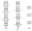
- the silicon layers are selectively removed from the layer stack first ( Fig. 1(b) ).
- etching by means of a wet alkaline solution is performed, e.g. in TMAH.
- the wet alkaline solution can for instance be or comprise TMAH, NaOH, KOH, EDP or NH4OH.
- the same solution will also etch the SiGe layer, although at a slower rate, the latter depending on the concentration of Silicon in the SiGe layer.
- the SiGe layer is exposed at its lower surface, allowing a much quicker removal of the SiGe layer as compared to the etching step which would only be acting on the sidewalls of the SiGe layer.
- the germanium layers then remain as nanowire channels ( Fig. 1(c) ).
- the upper surface of the substrate whereon the layer stack is grown has a (100) orientation.
- the sidewall/facets off the layers stacks can have a (110) and (111) direction respectively.
- the lower/upper layers of the layer stack thus have the same orientation.
- Si will be removed first in the stack and the attack of the harder layer to remove (SiGe) can occur from the (100) plane rather from the (110) sidewall/(111) facets.
- the alkaline etch rate of SiGe becomes very low ( ⁇ 1 nm/min) for SiGe with Ge concentrations > 30% (Si% ⁇ 70%).
- selectively etch SiGe to Ge alkaline selective etch is preferably done at high temperature, for instance at temperatures within the range of 70 to 90oC.
- all oxidizing species are removed from the etching solution (i.e. they are not present in the etching solution), as for instance dissolved oxygen and traces of hydrogen peroxide. This will strongly limit the selective etch to the sacrificial layers only. It was found that if the oxidizing species are present, at these high temperatures, an isotropic or less selective etch process occurs.
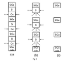
- the germanium layers are selectively removed from the layer stack first Fig. 2(b) .
- Selectively removing the silicon layers comprises performing for instance a HCl gas phase etch, a CF4 dry etch or etch with a APM (Ammonia and hydrogen Peroxide Mixture). The same solution will also etch the SiGe layer, although at a slower rate, the latter depending on the concentration of germanium in the SiGe layer.
- the SiGe layer is exposed at its upper surface, allowing a much quicker removal of the SiGe layer as compared to the etching step which would only be acting on the sidewalls of the SiGe layer.
- the silicon layers then remain as nanowire channels ( Fig. 2(c) ).
- both silicon and germanium layers are selectively removed, such that the silicon germanium layers remain as nanowire channels.
- First the Si can be removed, followed by the removal of the Ge layer.
- first the Ge can be removed (see Fig. 3(b) ), followed by the removal of the Si layer ( Fig. 3(c) ).
- Selectively removing the germanium layer can comprise etching with a solution of 03 and deionised water (DIW) or O3/HCl or O3/NH4OH.
- Selectively removing the silicon layer can comprise etching in a wet alkaline solution (for examples, see embodiments of the first type).
- the silicon germanium layers then remain as nanowire channels ( Fig. 3(c) ).
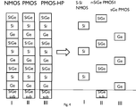
- Fig. 4 a further preferred embodiment is illustrated, wherein, based on a common stack of layers, the embodiments of the first (I), second (II) and third type are applied on the same substrate (III) in respective first, second and third regions.
- Appropriate masking steps may be applied in order to protect one or more of the regions when etching is performed in another region.
- the removal step of sacrificial layers (e.g. two out of three layers of a basic layer stack) in the layer stack can be based on an isotropic process or an anisotropic process.
- anisotropic processes it is preferred to take into account the crystal plane orientations, as the anisotropic process/etching is also dependent on the crystal plane.
- the skilled person will recognise that taking into account the crystal plane orientations of course needs to be consistent with final device requirements.
- Si and SiGe have shown anisotropic etch behavior in wet alkaline solutions.
- the etch rate of Si (001) and (110) crystal planes are much higher than the (111) and planes.
- the etch rates of the (100), (110) and (111) crystal planes are of the same order of magnitude, with the (110) crystal plane having the lowest etch rate.
- Si and SiGe also show anisotropic etch behavior during HCl gas phase etching.
- the etch rate of (100) crystallographic planes is higher compared to the (110) crystal planes.
- Anisotropic selective etch chemistries behave differently for convex (outward) and concave (inward) corners.
- anisotropic etching the etch rate of convex corners is determined by the crystallographic plane with the highest etch rate while the etch rate of concave corners is determined by the crystallographic plane with the lowest etch rate.
- Anisotropic selective etching thus forms concave corners in the sacrificial layer.
- the remaining nanowire has convex shape.
- the etch selectivity is then also determined by the slowest etching plane of the sacrificial layer versus the fastest etch rate of the nanowire.
- the selective etch is made 'easier' by the implementation of two sacrificial layers within the stack.
- the hardest-to-remove sacrificial layer will have convex corners, as well as the remaining nanowire layer.
- An appropriate etch selectivity can thus be then determined by comparing the crystal planes with the highest etch rates, both for the sacrificial layer and nanowire.
- Selective etch can also be done using isotropic selective etch chemistries, e.g. using formulated chemistries. By splitting up the sacrificial layer into different layers, the hardest- to-remove sacrificial layer will be etched from three directions as compared to two for a single sacrificial layer. This should reduce the required etch time and so increases the selectivity of the selective removal step.
- one of the layers can serve as a sacrificial layer, making the selective etch of SiGe towards the other layer easier/shorter.
- TMAH TMAH as selective etch of SiGe to Ge
- Silicon can be very easily etched out, giving more easy access for the selective etch chemical towards SiGe removal.
- Similar advantage can also be applied for selective etch of SiGe towards Silicon (e.g. using HCl vapour etch will remove Ge very fastly, thus allowing isotropic SiGe etch by HCl from 3 sides rather than left/right site of the stack only.
- Si channel transistors in this case the Si material can be used for NMOS transistors, either High Performance or Low Power applications
- SiGe channel transistors PMOS, Low Power application
- Ge channel transistors PMOS, High Performance application
Landscapes
- Engineering & Computer Science (AREA)
- Chemical & Material Sciences (AREA)
- Nanotechnology (AREA)
- Physics & Mathematics (AREA)
- Crystallography & Structural Chemistry (AREA)
- General Physics & Mathematics (AREA)
- Manufacturing & Machinery (AREA)
- Condensed Matter Physics & Semiconductors (AREA)
- Mathematical Physics (AREA)
- Theoretical Computer Science (AREA)
- Thin Film Transistor (AREA)
- Metal-Oxide And Bipolar Metal-Oxide Semiconductor Integrated Circuits (AREA)
- Plasma & Fusion (AREA)
- Insulated Gate Type Field-Effect Transistor (AREA)
- Recrystallisation Techniques (AREA)
Abstract
- providing a substrate;
- growing a layer stack on the substrate in at least a first channel region, the layer stack comprising a plurality of basic layer stacks, the basic layer stack comprising a first silicon germanium layer, a second silicon germanium layer and a third silicon germanium layer in a predetermined order, the first, second and third silicon germanium layers having substantially different germanium concentrations;
- selectively removing a first layer of each of the basic layer stacks, with respect to a second and a third layer of the respective stack, thereby creating gaps in the layer stack where the first layers were present before;
- selectively removing a second layer of each of the basic layer stacks, with respect to the third layer, wherein the removal of the second layer occurs at least partially from within the gaps, thereby defining the nanowire channels; and associated CMOS devices.
Description
- The present disclosure relates to transistor devices comprising multiple nanowire channels, and associated CMOS devices.
- Moore's Law defines a roadmap for scaling semiconductor devices in CMOS technology. In order to be able to further scale CMOS devices in the future, silicon CMOS technology is being complemented or replaced by technology based on other material systems.
- Gate-all-around devices on nanowires, wherein gates are provided which completely surround nanowire channel structures of a transistor, are required to improve the short channel control of advanced node devices in order to allow continued gate length scaling.
- Moreover, in order to keep drive per chip area, multiple wires will have to be used which are positioned vertically above each other, in a predetermined gate region having limited foot print.
- Another trend in CMOS processing, is to combine different semiconductor materials as channel materials on the same substrate, for instance for use as NMOS and PMOS devices respectively.
- In
US 2013/0270512 A1 NMOS and PMOS nanowire devices are disclosed wherein both NMOS and PMOS devices comprise a vertical stack of nanowires to achieve a greater current carrying capability (e.g. larger drive currents) for a given device footprint over a substrate. The NMOS nanowire transistor comprises group III-V semiconductor material, e.g. GaAs, while the PMOS nanowire comprises group IV semiconductor material, e.g. Germanium. In some embodiments, both NMOS and PMOS device fabrication comprises the growth of a single stack of layers wherein alternatingly a layer of a group IV semiconductor material and a layer of a group III-V semiconductor material are grown on top of each other. In an NMOS region, the group IV semiconductor layer is then selectively removed, while in a PMOS region the group III-V semiconductor layer is selectively removed. - There exists a need in industry to provide alternative solutions which allow the combination of more than two different semiconductor materials as channel materials on the same substrate.
- It is an aim of the present disclosure to provide a method for manufacturing a transistor device comprising multiple nanowire channels arranged above one another in a vertical stack, which allow the combination of more than two different semiconductor materials as channel materials on the same substrate.
- This aim is achieved according to the disclosure with the method showing the technical characteristics of the first independent claim.
- It is another aim of the present disclosure to provide an associated CMOS device.
- In a first aspect of the present disclosure a method is disclosed for manufacturing a transistor device comprising multiple nanowire channels arranged above one another in a vertical stack, the method comprising
- providing a substrate;
- growing a layer stack on said substrate in at least a first channel region, said layer stack comprising a plurality of basic layer stacks, said basic layer stack comprising a first silicon germanium layer, a second silicon germanium layer and a third silicon germanium layer in a predetermined order, the first, second and third silicon germanium layers having substantially different germanium concentrations;
- selectively removing a first layer of each of said basic layer stacks, with respect to a second and a third layer of said respective stack, thereby creating gaps in said layer stack where said first layers were present before;
- selectively removing a second layer of each of said basic layer stacks, with respect to said third layer, wherein said removal of said second layer occurs at least partially from within said gaps, thereby defining said nanowire channels.
- In a specific embodiment, the method comprises
- providing a substrate;
- growing a layer stack on the substrate in at least a first channel region, the layer stack comprising a plurality of basic layer stacks, the basic layer stack comprising (or consisting of) a silicon layer, a silicon germanium layer and a germanium layer in a predetermined order;
- selectively removing a first layer of each of the basic layer stacks, with respect to a second and a third layer of the respective stack, thereby creating gaps in the layer stack where the first layers were present before;
- selectively removing a second layer of each of the basic layer stacks, with respect to the third layer, wherein the removal of the second layer occurs at least partially from within the gaps, thereby defining the nanowire channels.
- It is an advantage that three different nanowire channel materials or three different stress-state nanowire materials can be provided on the same substrate, by means of a common initial process flow.
- Moreover, when the first layer of the three layers of the basic layer stacks is removed selectively, a gap is created within the stack, providing access to the second layer of the three layers of the basic layer stack. This allows a relatively quick and efficient selective removal of the second layer.
- The first selective removal step and the second selective removal step may be independent steps or may comprise a single step. In case a single step is performed, e.g. a single etch step, this is such that the first layer is removed first at a much higher speed than the second layer. Once the first layer has been removed, the removal of the second layer can proceed in an accelerated manner as its upper or lower surface is then exposed to the etching substance.
- According to preferred embodiments, the method may further comprise performing a recess etch creating recesses in between STI structures in a substrate, and growing the layer stack within said recesses. Alternatively, the layer stack can be grown on a blanked wafer, and can then be patterned into fin-type structures, protruding from the substrate.
- According to preferred embodiments of a first type, the first layer has a relatively low germanium concentration, the second layer has a relatively average silicon germanium concentration and the third layer has a relatively high germanium concentration, and selectively removing the first layer and selectively removing the second layer comprises etching in a wet alkaline solution.
- For instance, the first layer can be a silicon layer, the second layer can be a silicon germanium layer and the third layer can be a germanium layer, and selectively removing the first layer and selectively removing the second layer comprises etching in a wet alkaline solution.
The wet alkaline solution can for instance be or comprise TMAH, NaOH, KOH, EDP or NH4OH. The germanium layer then remains as a nanowire channel. - According to preferred embodiments of a second type, the first layer has a relatively high germanium concentration, the second layer has a relatively average germanium concentration and the third layer has a relatively low germanium concentration, and selectively removing the first layer and selectively removing the second layer comprises a HCl gas phase etch, a CF4 dry etch or etch with a APM.
- For instance, the first layer can be a germanium layer, the second layer can be a silicon germanium layer and the third layer can be a silicon layer, selectively removing the first layer and selectively removing the second layer can comprise a HCl gas phase etch, a CF4 dry etch or etch with a APM (Ammonia and hydrogen Peroxide Mixture).
- The silicon layer then remains as a nanowire channel.
- According to preferred embodiments of a third type, the first layer has a relatively high germanium concentration, the second layer has a relatively low germanium concentration and the third layer has a relatively average germanium concentration, selectively removing the first layer comprises etching with O3/deionised water (DIW), O3HCl or O3/NH4OH, and selectively removing the second layer comprises etching in a wet alkaline solution.
- For instance, the first layer can be a germanium layer, the second layer can be a silicon layer and the third layer can be a silicon germanium layer, selectively removing the first layer can comprise etching with O3/deionised water (DIW) and selectively removing the second layer can comprise etching in a wet alkaline solution (for examples, see embodiments of the first type).
- The silicon germanium layer then remains as a nanowire channel.
- According to preferred embodiments, the method comprises
- growing a layer stack on the substrate in at least a first, as second and a third channel region, the layer stack comprising a plurality of basic layer stacks, the basic layer stack comprising a silicon layer, a silicon germanium layer and a germanium layer in a predetermined order;
- applying the method according to embodiments of the first type in the first channel region;
- applying the method according to embodiments of the second type in the second channel region;
- applying the method according to embodiments of the third type in the third channel region.
- The first, second and third channel regions preferably correspond respectively to a high performance PMOS (Germanium nanowire channels), an NMOS (silicon naowire channels) and a PMOS (SiGe nanowire channels) nanowire transistor. According to preferred embodiments, the method comprises providing one or more gate structures provided all around the nanowire channels.
- According to preferred embodiments, the predetermined order of the relatively low germanium concentration silicon germanium layer, the relatively average germanium concentration silicon germanium layer and the relatively high germanium concentration silicon germanium layer is: relatively high germanium concentration silicon germanium layer - relatively low germanium concentration silicon germanium layer - relatively average germanium concentration silicon germanium.
- For instance, the predetermined order of a silicon layer, a silicon germanium layer and a germanium layer is: germanium - silicon - silicon germanium from lower layer to upper layer.
- According to alternative preferred embodiments, the predetermined order of the relatively low germanium concentration silicon germanium layer, the relatively average germanium concentration silicon germanium layer and the relatively high germanium concentration silicon germanium layer is : relatively high germanium concentration silicon germanium layer - relatively average germanium concentration silicon germanium layer - relatively low germanium concentration silicon germanium layer from lower layer to upper layer.
- For instance, the predetermined order of a silicon layer, a silicon germanium layer and a germanium layer is: germanium - silicon germanium - silicon from lower layer to upper layer.
- According to preferred embodiments, the substrate is a strain relaxed buffer (SRB) SiGe substrate or a silicon substrate, and the Germanium layers of the basic layer stacks are grown with compressive stress, the Silicon layers of the basic layer stacks are grown with tensile stress, and the SiGe layers of the basic layer stacks are grown such that they are relaxed or strained.
- It is an advantage that the presence of plurality of basic layer stacks having the above stress relation, stabilizes the layer stack. Indeed, this may lead to a larger amount of strain in the layer stack and/or more wires and/or thicker wires which are suitable for being used as wire channels.
- According to preferred embodiments, growing the layer stack comprises subsequently growing a plurality of basic layer stacks directly on top of one another. Preferably, the basic layer stacks are identical in constitution.
- According to preferred embodiments, a single layer stack is applied over a main surface of the substrate, and is then patterned. After patterning the layer stack can still be present in the first region, or for instance in the first region, second region and third region.
- In a second aspect of the present invention, a CMOS device is disclosed comprising at least three types of transistor devices arranged in a substrate, wherein each type of transistor device comprises multiple nanowire channels arranged above one another in a vertical stack, wherein the nanowire channels of the same type of transistor device comprise the same materials, and wherein a first type of transistor device comprises Si nanowire channels, a second type of transistor device comprises Ge nanowire channels, and a third type of transistor device comprises SiGe nanowire channels.
- According to preferred embodiments, the nanowire channels of the different types of transistor devices are arranged at different, non-overlapping height ranges above the substrate. In other words, the nanowire channels of different types of transistor devices may be off-set in the height direction.
- According to a further aspect of the present disclosure, the removal of a SiGe layer with a Ge concentration x with respect to a (preferably interfacing) SiGe layer with a Ge concentration y, with y>x, is performed in an alkaline solution as described before, at temperatures within the range of 70 to 90ºC. Preferably, all oxidizing species are removed from the etching solution (i.e. they are not present in the etching solution), as for instance dissolved oxygen and traces of hydrogen peroxide. This will strongly limit the selective etch to the low concentration Ge layer only. It was found that if the oxidizing species are present, at these high temperatures, an isotropic or less selective etch process occurs.
- This can be combined with any of the embodiments of the first aspect of the present invention, wherein a selective removal of a SiGe layer with a Ge concentration x with respect to a (e.g. interfacing) SiGe layer with a Ge concentration with a concentration y, with y>x is performed, for instance where a SiGe layer in the layer stack (e.g. basic layer stack) is selectively removed with respect to a Ge layer in the layer stack (e.g. basic layer stack).
Features and advantages disclosed for one of the above aspects of the present invention are hereby also implicitly disclosed the other aspects, mutatis mutandis, as the skilled person will recognize. - Certain objects and advantages of various inventive aspects have been described herein above. It is understood that this summary is merely an example and is not intended to limit the scope of the disclosure. The disclosure, both as to organization and method of operation, together with features and advantages thereof, may best be understood by reference to the following detailed description when read in conjunction with the accompanying drawings.
- The disclosure will be further elucidated by means of the following description and the appended figures.
-
Figures 1(a) to 1(c) illustrate a first embodiment of the present invention. -
Figures 2(a) to 2(c) illustrate a second embodiment of the present invention. -
Figure 3(a) to 3(c) illustrates a third embodiment of the present invention. -
Figure 4 illustrates a fourth embodiment of the present invention. - The present disclosure will be described with respect to particular embodiments and with reference to certain drawings but the disclosure is not limited thereto but only by the claims. The drawings described are only schematic and are nonlimiting. In the drawings, the size of some of the elements may be exaggerated and not drawn on scale for illustrative purposes. The dimensions and the relative dimensions do not necessarily correspond to actual reductions to practice of the disclosure.
- Furthermore, the various embodiments, although referred to as "preferred" are to be construed as examples by which the disclosure may be implemented rather than as limiting the scope of the disclosure.
- Gate-all-around devices on nanowires are required to improve the short channel control of advanced node devices in order to allow continued gate length scaling.
- In order to keep drive per chip area, multiple wires need to be used which are arranged above one another, in a vertical stack, being spaced apart by respective gaps.
- In an aspect of the present invention, a method is disclosed for fabricating tensile-strained Si wires (typically used for NMOS), strained or unstrained SiGe wires (typically used for PMOS) and compressively-strained Ge wires (typically used for High Performance (HP) PMOS) on a common substrate.
- More generally, a method is disclosed for fabricating tensile-strained SiGe wires (typically used for NMOS), strained or unstrained SiGe wires (typically used for PMOS) and compressive-strained SiGe wires (typically used for High Performance (HP) PMOS) on a common substrate. The tensile-strained, compressive strained and unstrained SiGe wires typically have a different germanium concentration.
- Hereby, a layer stack is grown on a substrate in at least a first channel region, the layer stack comprising a plurality of basic layer stacks, the basic layer stack comprising a first silicon germanium layer, a second silicon germanium layer and a third silicon germanium layer in a predetermined order, the first, second and third silicon germanium layers having substantially different germanium concentrations. For instance, one of the three silicon germanium layers has a relatively low germanium concentration, another of the three silicon germanium layers has a relatively average silicon germanium concentration and another of the three silicon germanium layers has a relatively high germanium concentration. The relatively low germanium concentration is preferably within the closed range of 0 to 50%. The relatively average germanium concentration is preferably within the closed range of 25 to 75 %. The relatively high germanium concentration is preferably within the closed range of 50 to 100%. Preferably, the relative difference in germanium concentration between any two of the three silicon germanium layers is larger than 10% or larger than 15% or larger than 20 %. The relatively average germanium concentration lies between the relatively high and the relatively low germanium concentrations.
- In the examples set out below, the relatively low germanium concentration silicon germanium layer is represented by a specific embodiments of being a silicon layer. The relatively high germanium concentration silicon germanium layer is represented by a specific embodiment of being a germanium layer.
- In different preferred embodiments of the present disclosure, explained into more detail in the paragraphs below, a SiGe strain relaxed Buffer (for instance having a Ge% concentration of the SRB ranging between 25% and 75%, more preferably between 40% to 60%, for instance of about 50%) is provided as a starting substrate layer. The SRB buffer layer can for instance be provided on a blanket wafer or can for instance be provided within recesses in between Shallow Trench Isolation (STI) structures on a substrate.
- A multi-layer stack of thin layers (for instance each having thicknesses below 10 nm) of tensile-strained Silicon, compressive-strained Germanium and relaxed or strained Silicon Germanium is grown. The different layers are provided in an alternating, regular manner, i.e. at least one iteration of the basic layer stack is provided. During the growth process, the different layers are grown below a certain thickness, such that no relaxation occurs and the layers remain crystalline. The thickness can remain below the critical thickness, such that the layer is stable, or below a certain stability guaranteeing thickness which is larger than the critical thickness and below which the layer is stable or meta stable.
- For instance, when growing a first basic layer stack, a Germanium layer can be grown on an underlying SiGe substrate layer (SRB layer), a silicon layer can be grown on top of the Germanium layer, and a SiGe layer can be grown on top of the underlying silicon layer. This is illustrated in
Fig. 1 (a) . The Germanium layers of the basic layer stacks are grown with compressive stress, the Silicon layers of the basic layer stacks are grown with tensile stress, and the SiGe layers of the basic layer stacks are grown such that they are relaxed or strained. A similar second basic layer stack can be grown on top, etc. Note that a different starting layer can be applied as a starting layer of the layer stack, such that the (e.g. first) basic layer stack itself can be seen as having a different starting layer. If the initial order is respected though, the original basic layer stack will then off course be retrieved higher in the stack, when growing the layer stack by growing basic layer stacks subsequently on top of each other. The main principle of aspects of the present invention remains the same. - Alternatively, the basic layer stack can for instance comprise the same three layers, but in another order. Starting with a Germanium layer which is grown on an underlying SiGe substrate layer (SRB layer), a SiGe layer can be grown on top of the Germanium layer, and a Si layer can be grown on top of the underlying SiGe layer. This results in layer stacks which are different from the layer stacks in the previous paragraph, but the main principle of aspects of the present invention remains the same. Also here, a different starting layer can be applied and, if the initial order is respected, the original basic layer stack will then off course be retrieved higher in the stack, when growing the layer stack by growing basic layer stacks subsequently on top of each other. The main principle of aspects of the present invention remains the same. These embodiments have not been illustrated.
- The layer stack is then patterned, such that fin structures are defined in at least a first region. Two of the three layers of the basis layer structure are then removed selectively, in one or more processing steps, for instance by means of (isotropic or anisotropic) etching, such that only the third layers remain and form nanowire structures, which can be used as a channel structure of a respective transistor.
- Different removal techniques or etching techniques can be applied, depending on the material eventually required for the nanowire, some of which are explained below in more detail, in relation with
Fig. 1 to 3 . - According to preferred embodiments, the embodiments explained in relation with
Fig. 1 to 3 are combined, such that, based on a common initial layer stack, different nanowires, i.e. nanowire materials are manufactured in a first, second and third region respectively. - Also, a gate can be provided all around the nanowire channels, according to techniques known to the skilled person. Source and drain regions and electrodes can also be provided, according to techniques known to the skilled person.
- In a preferred embodiment of the first type, starting from the layer stack depicted in
Fig. 1 (a) , the silicon layers are selectively removed from the layer stack first (Fig. 1(b) ). Hereto, etching by means of a wet alkaline solution is performed, e.g. in TMAH. The wet alkaline solution can for instance be or comprise TMAH, NaOH, KOH, EDP or NH4OH. The same solution will also etch the SiGe layer, although at a slower rate, the latter depending on the concentration of Silicon in the SiGe layer. Once the silicon layer is removed, which occurs relatively quickly, the SiGe layer is exposed at its lower surface, allowing a much quicker removal of the SiGe layer as compared to the etching step which would only be acting on the sidewalls of the SiGe layer. The germanium layers then remain as nanowire channels (Fig. 1(c) ). - Typically, the upper surface of the substrate whereon the layer stack is grown has a (100) orientation. The sidewall/facets off the layers stacks can have a (110) and (111) direction respectively. The lower/upper layers of the layer stack thus have the same orientation. In such a configuration, Si will be removed first in the stack and the attack of the harder layer to remove (SiGe) can occur from the (100) plane rather from the (110) sidewall/(111) facets.
- The alkaline etch rate of SiGe becomes very low (< 1 nm/min) for SiGe with Ge concentrations > 30% (Si% < 70%). In order to selectively etch SiGe to Ge alkaline selective etch is preferably done at high temperature, for instance at temperatures within the range of 70 to 90ºC. Preferably, all oxidizing species are removed from the etching solution (i.e. they are not present in the etching solution), as for instance dissolved oxygen and traces of hydrogen peroxide. This will strongly limit the selective etch to the sacrificial layers only. It was found that if the oxidizing species are present, at these high temperatures, an isotropic or less selective etch process occurs.
- According to preferred embodiments of the second type, starting from the layer stack depicted in
Fig. 2(a) (1 (a)), the germanium layers are selectively removed from the layer stack firstFig. 2(b) . Selectively removing the silicon layers comprises performing for instance a HCl gas phase etch, a CF4 dry etch or etch with a APM (Ammonia and hydrogen Peroxide Mixture). The same solution will also etch the SiGe layer, although at a slower rate, the latter depending on the concentration of germanium in the SiGe layer. Once the germanium layer is removed, which occurs relatively quickly, the SiGe layer is exposed at its upper surface, allowing a much quicker removal of the SiGe layer as compared to the etching step which would only be acting on the sidewalls of the SiGe layer. The silicon layers then remain as nanowire channels (Fig. 2(c) ). - According to preferred embodiments of a third type, starting from the layer stack depicted in
Fig. 3(a) (1(a), 2(a)), both silicon and germanium layers are selectively removed, such that the silicon germanium layers remain as nanowire channels.
First the Si can be removed, followed by the removal of the Ge layer. Alternatively, first the Ge can be removed (seeFig. 3(b) ), followed by the removal of the Si layer (Fig. 3(c) ). - Selectively removing the germanium layer can comprise etching with a solution of 03 and deionised water (DIW) or O3/HCl or O3/NH4OH. Selectively removing the silicon layer can comprise etching in a wet alkaline solution (for examples, see embodiments of the first type).
The silicon germanium layers then remain as nanowire channels (Fig. 3(c) ). - In
Fig. 4 , a further preferred embodiment is illustrated, wherein, based on a common stack of layers, the embodiments of the first (I), second (II) and third type are applied on the same substrate (III) in respective first, second and third regions. - Appropriate masking steps may be applied in order to protect one or more of the regions when etching is performed in another region.
- It is believed that a multi-layer stack of Si, SiGe and Ge layers or nanowires, co-integrated on a SRB SiGe substrate (for instance Ge%=50%) is more stable than a fully strained Ge or strained Si directly grown on such a SRB substrate.
- Indeed, it is believed that tensile strained Silicon and compressively strained Ge balance each other out in a layer stack of thin layers. This means that the fin structures made from the multistack layer are able to withstand higher thermal budgets as compared to single, relatively tall, strained Ge or strained Silicon fin structures.
- The removal step of sacrificial layers (e.g. two out of three layers of a basic layer stack) in the layer stack can be based on an isotropic process or an anisotropic process. In case anisotropic processes are used, it is preferred to take into account the crystal plane orientations, as the anisotropic process/etching is also dependent on the crystal plane. The skilled person will recognise that taking into account the crystal plane orientations of course needs to be consistent with final device requirements.
- E.g. Si and SiGe have shown anisotropic etch behavior in wet alkaline solutions. In alkaline solutions, the etch rate of Si (001) and (110) crystal planes are much higher than the (111) and planes. For the case of SiGe the etch rates of the (100), (110) and (111) crystal planes are of the same order of magnitude, with the (110) crystal plane having the lowest etch rate.
Further, e.g., Si and SiGe also show anisotropic etch behavior during HCl gas phase etching. The etch rate of (100) crystallographic planes is higher compared to the (110) crystal planes. - Anisotropic selective etch chemistries behave differently for convex (outward) and concave (inward) corners. During anisotropic etching the etch rate of convex corners is determined by the crystallographic plane with the highest etch rate while the etch rate of concave corners is determined by the crystallographic plane with the lowest etch rate. Anisotropic selective etching thus forms concave corners in the sacrificial layer. The remaining nanowire has convex shape. The etch selectivity is then also determined by the slowest etching plane of the sacrificial layer versus the fastest etch rate of the nanowire.
By application of the nanowire stack as proposed in embodiments of the present disclosure, the selective etch is made 'easier' by the implementation of two sacrificial layers within the stack. The hardest-to-remove sacrificial layer will have convex corners, as well as the remaining nanowire layer. - An appropriate etch selectivity can thus be then determined by comparing the crystal planes with the highest etch rates, both for the sacrificial layer and nanowire.
- Selective etch can also be done using isotropic selective etch chemistries, e.g. using formulated chemistries. By splitting up the sacrificial layer into different layers, the hardest- to-remove sacrificial layer will be etched from three directions as compared to two for a single sacrificial layer. This should reduce the required etch time and so increases the selectivity of the selective removal step.
- Aspects of the present disclosure provide various advantages.
- It is an advantage that combining the compressive Ge and tensile Si in a multi-layer stack as disclosed stabilizes the layer stack, allowing larger amount of strain and/or more wires and/or thicker wires.
- It is a further advantage that, in a multi-layer stack as disclosed, one of the layers can serve as a sacrificial layer, making the selective etch of SiGe towards the other layer easier/shorter. E.g. Using TMAH as selective etch of SiGe to Ge, Silicon can be very easily etched out, giving more easy access for the selective etch chemical towards SiGe removal. Similar advantage can also be applied for selective etch of SiGe towards Silicon (e.g. using HCl vapour etch will remove Ge very fastly, thus allowing isotropic SiGe etch by HCl from 3 sides rather than left/right site of the stack only.
- It is an even further advantage that, having the three different nanowire channel materials, allows combination of Si channel transistors (in this case the Si material can be used for NMOS transistors, either High Performance or Low Power applications), SiGe channel transistors (PMOS, Low Power application) and Ge channel transistors (PMOS, High Performance application) on a single, common substrate.
- The foregoing description details certain embodiments of the disclosure. It will be appreciated, however, that no matter how detailed the foregoing appears in text, the disclosure may be practiced in many ways.
- While the above detailed description has shown, described, and pointed out novel features of the invention as applied to various embodiments, it will be understood that various omissions, substitutions, and changes in the form and details of the device or process illustrated may be made by those skilled in the technology without departing from the disclosure.
Claims (12)
- A method for manufacturing a transistor device comprising multiple nanowire channels arranged above one another in a vertical stack, comprising- providing a substrate;- growing a layer stack on said substrate in at least a first channel region, said layer stack comprising a plurality of basic layer stacks, said basic layer stack comprising a first silicon germanium layer, a second silicon germanium layer and a third silicon germanium layer in a predetermined order, the first, second and third silicon germanium layers having substantially different germanium concentrations;- selectively removing a first layer of each of said basic layer stacks, with respect to a second and a third layer of said respective stack, thereby creating gaps in said layer stack where said first layers were present before;- selectively removing a second layer of each of said basic layer stacks, with respect to said third layer, wherein said removal of said second layer occurs at least partially from within said gaps, thereby defining said nanowire channels.
- A method according to claim 1, wherein said first layer has a relatively low germanium concentration, said second layer has a relatively average silicon germanium concentration and said third layer has a relatively high germanium concentration, wherein selectively removing the first layer and selectively removing the second layer comprises etching in a wet alkaline solution.
- A method according to claim 1, wherein said first layer has a relatively high germanium concentration, said second layer has a relatively average germanium concentration and said third layer has a relatively low germanium concentration, wherein selectively removing the first layer and selectively removing the second layer comprises a HCl gas phase etch, a CF4 dry etch or etch with a APM.
- A method according to claim 1, wherein said first layer has a relatively high germanium concentration, said second layer has a relatively low germanium concentration and said third layer has a relatively average germanium concentration, wherein selectively removing the first layer comprises etching with O3/deionised water (DIW) or O3/HCl or O3/NH4OH, and wherein selectively removing the second layer comprises etching in a wet alkaline solution.
- A method according to claim 1, comprising- growing said layer stack on said substrate in at least a first, as second and a third channel region, said layer stack comprising a plurality of basic layer stacks, said basic layer stack comprising a silicon layer, a silicon germanium layer and a germanium layer in a predetermined order;- applying the method according to claim 2 in the first channel region;- applying the method according to claim 3 in the second channel region;- applying the method according to claim 4 in the third channel region.
- A method according to any of the previous claims, further comprising providing one or more gate structures provided all around said nanowire channels.
- A method according to any of the previous claims, wherein said predetermined order of said relatively low germanium concentration silicon germanium layer, said relatively average germanium concentration silicon germanium layer and said relatively high germanium concentration silicon germanium layer is relatively high germanium concentration silicon germanium layer - relatively low germanium concentration silicon germanium layer - relatively average germanium concentration silicon germanium layer.
- A method according to any of the previous claims 1 to 6, wherein said predetermined order of said relatively low germanium concentration silicon germanium layer, said relatively average germanium concentration silicon germanium layer and said relatively high germanium concentration silicon germanium layer is relatively high germanium concentration silicon germanium layer - relatively average germanium concentration silicon germanium layer - relatively low germanium concentration silicon germanium layer from lower layer to upper layer.
- A method according to any of the previous claims, wherein said substrate is a strain relaxed buffer (SRB) SiGe substrate or a silicon substrate, and wherein said Germanium layers of said basic layer stacks are grown with compressive stress, said Silicon layers of said basic layer stacks are grown with tensile stress, and said SiGe layers of said basic layer stacks are grown such that they are relaxed or strained.
- A method according to any of the previous claims, wherein growing said layer stack comprises subsequently growing a plurality of basic layer stacks directly on top of one another.
- A CMOS device comprising at least three types of transistor devices arranged in a substrate, wherein each said type of transistor device comprises multiple nanowire channels arranged above one another in a vertical stack, wherein the nanowire channels of the same type of transistor device comprise the same materials, and wherein a first type of transistor device comprises Si nanowire channels, a second type of transistor device comprises Ge nanowire channels, and a third type of transistor device comprises SiGe nanowire channels.
- A CMOS device according to claim 11, wherein said nanowire channels of the different types of transistor devices are arranged at different, non-overlapping height ranges above the substrate.
Priority Applications (2)
| Application Number | Priority Date | Filing Date | Title |
|---|---|---|---|
| EP15174968.6A EP3112316B1 (en) | 2015-07-02 | 2015-07-02 | Method for manufacturing transistor devices comprising multiple nanowire channels |
| US15/199,535 US9842777B2 (en) | 2015-07-02 | 2016-06-30 | Semiconductor devices comprising multiple channels and method of making same |
Applications Claiming Priority (1)
| Application Number | Priority Date | Filing Date | Title |
|---|---|---|---|
| EP15174968.6A EP3112316B1 (en) | 2015-07-02 | 2015-07-02 | Method for manufacturing transistor devices comprising multiple nanowire channels |
Publications (2)
| Publication Number | Publication Date |
|---|---|
| EP3112316A1 true EP3112316A1 (en) | 2017-01-04 |
| EP3112316B1 EP3112316B1 (en) | 2018-05-02 |
Family
ID=53498917
Family Applications (1)
| Application Number | Title | Priority Date | Filing Date |
|---|---|---|---|
| EP15174968.6A Active EP3112316B1 (en) | 2015-07-02 | 2015-07-02 | Method for manufacturing transistor devices comprising multiple nanowire channels |
Country Status (2)
| Country | Link |
|---|---|
| US (1) | US9842777B2 (en) |
| EP (1) | EP3112316B1 (en) |
Cited By (4)
| Publication number | Priority date | Publication date | Assignee | Title |
|---|---|---|---|---|
| CN109427901A (en) * | 2017-08-31 | 2019-03-05 | 台湾积体电路制造股份有限公司 | Semiconductor devices and methods |
| TWI731350B (en) * | 2018-06-26 | 2021-06-21 | 台灣積體電路製造股份有限公司 | Integrated circuit and manufacturing method thereof |
| US20240088252A1 (en) * | 2022-09-08 | 2024-03-14 | International Business Machines Corporation | Gate all around transistors with heterogeneous channels |
| US12369387B2 (en) | 2017-08-31 | 2025-07-22 | Taiwan Semiconductor Manufacturing Company, Ltd. | Semiconductor device and method |
Families Citing this family (22)
| Publication number | Priority date | Publication date | Assignee | Title |
|---|---|---|---|---|
| US9899387B2 (en) * | 2015-11-16 | 2018-02-20 | Taiwan Semiconductor Manufacturing Company, Ltd. | Multi-gate device and method of fabrication thereof |
| US9484267B1 (en) * | 2016-02-04 | 2016-11-01 | International Business Machines Corporation | Stacked nanowire devices |
| CA3022278C (en) | 2016-02-08 | 2021-06-08 | The Sherwin-Williams Company | Folding tool |
| US10236362B2 (en) * | 2016-06-30 | 2019-03-19 | International Business Machines Corporation | Nanowire FET including nanowire channel spacers |
| US9793398B1 (en) * | 2016-08-02 | 2017-10-17 | International Business Machines Corporation | Fabrication of a strained region on a substrate |
| US10128347B2 (en) | 2017-01-04 | 2018-11-13 | International Business Machines Corporation | Gate-all-around field effect transistor having multiple threshold voltages |
| US11245020B2 (en) * | 2017-01-04 | 2022-02-08 | International Business Machines Corporation | Gate-all-around field effect transistor having multiple threshold voltages |
| US10199485B2 (en) * | 2017-01-18 | 2019-02-05 | United Microelectronics Corp. | Semiconductor device including quantum wires |
| US10553495B2 (en) | 2017-10-19 | 2020-02-04 | International Business Machines Corporation | Nanosheet transistors with different gate dielectrics and workfunction metals |
| FR3073666B1 (en) | 2017-11-14 | 2019-11-22 | Commissariat A L'energie Atomique Et Aux Energies Alternatives | METHOD FOR MANUFACTURING FIELD EFFECT TRANSISTOR |
| US10355102B2 (en) | 2017-11-15 | 2019-07-16 | Taiwan Semiconductor Manufacturing Co., Ltd. | Semiconductor device and method of manufacturing the same |
| US10685887B2 (en) * | 2017-12-04 | 2020-06-16 | Tokyo Electron Limited | Method for incorporating multiple channel materials in a complimentary field effective transistor (CFET) device |
| KR102452925B1 (en) | 2018-02-23 | 2022-10-07 | 삼성전자주식회사 | Semiconductor device and method for fabricating the same |
| US11031395B2 (en) * | 2018-07-13 | 2021-06-08 | Taiwan Semiconductor Manufacturing Co., Ltd. | Method of forming high performance MOSFETs having varying channel structures |
| US11152510B2 (en) | 2018-07-25 | 2021-10-19 | International Business Machines Corporation | Long channel optimization for gate-all-around transistors |
| US10756175B2 (en) | 2018-09-18 | 2020-08-25 | International Business Machines Corporation | Inner spacer formation and contact resistance reduction in nanosheet transistors |
| US11469299B2 (en) * | 2018-09-28 | 2022-10-11 | Intel Corporation | Gate-all-around integrated circuit structures having underlying dopant-diffusion blocking layers |
| US11101360B2 (en) * | 2018-11-29 | 2021-08-24 | Taiwan Semiconductor Manufacturing Co., Ltd. | Method of manufacturing a semiconductor device and a semiconductor device |
| US11424347B2 (en) * | 2020-06-11 | 2022-08-23 | Taiwan Semiconductor Manufacturing Co., Ltd. | Semiconductor device and method |
| US20220406776A1 (en) * | 2021-06-21 | 2022-12-22 | International Business Machines Corporation | Stacked fet with different channel materials |
| US11764058B2 (en) * | 2021-09-28 | 2023-09-19 | Applied Materials, Inc. | Three-color 3D DRAM stack and methods of making |
| US12310062B2 (en) | 2021-11-11 | 2025-05-20 | Samsung Electronics Co., Ltd. | Integrated circuit devices including stacked transistors and methods of forming the same |
Citations (6)
| Publication number | Priority date | Publication date | Assignee | Title |
|---|---|---|---|---|
| WO2012074872A2 (en) * | 2010-12-01 | 2012-06-07 | Intel Corporation | Silicon and silicon germanium nanowire structures |
| WO2013095341A1 (en) * | 2011-12-19 | 2013-06-27 | Intel Corporation | Cmos implementation of germanium and iii-v nanowires and nanoribbons in gate-all-around architecture |
| WO2013095650A1 (en) * | 2011-12-23 | 2013-06-27 | Intel Corporation | Nanowire structures having non-discrete source and drain regions |
| WO2014051723A1 (en) * | 2012-09-28 | 2014-04-03 | Intel Corporation | Non-planar semiconductor device having germanium-based active region with release etch-passivation surface |
| US20150053928A1 (en) * | 2013-08-20 | 2015-02-26 | Taiwan Semiconductor Manufacturing Company Limited | Silicon and silicon germanium nanowire formation |
| WO2015094301A1 (en) * | 2013-12-19 | 2015-06-25 | Intel Corporation | Non-planar semiconductor device having hybrid geometry-based active region |
Family Cites Families (9)
| Publication number | Priority date | Publication date | Assignee | Title |
|---|---|---|---|---|
| KR100481209B1 (en) | 2002-10-01 | 2005-04-08 | 삼성전자주식회사 | MOS Transistor having multiple channels and method of manufacturing the same |
| US8293608B2 (en) * | 2008-02-08 | 2012-10-23 | Freescale Semiconductor, Inc. | Intermediate product for a multichannel FET and process for obtaining an intermediate product |
| US8183104B2 (en) | 2010-07-07 | 2012-05-22 | Hobbs Christopher C | Method for dual-channel nanowire FET device |
| WO2013095646A1 (en) * | 2011-12-23 | 2013-06-27 | Intel Corporation | Cmos nanowire structure |
| US9224808B2 (en) * | 2011-12-23 | 2015-12-29 | Intel Corporation | Uniaxially strained nanowire structure |
| KR101678405B1 (en) | 2012-07-27 | 2016-11-22 | 인텔 코포레이션 | Nanowire transistor devices and forming techniques |
| US9576856B2 (en) * | 2014-10-27 | 2017-02-21 | Globalfoundries Inc. | Fabrication of nanowire field effect transistor structures |
| US10038053B2 (en) * | 2015-10-12 | 2018-07-31 | International Business Machines Corporation | Methods for removal of selected nanowires in stacked gate all around architecture |
| US10074730B2 (en) * | 2016-01-28 | 2018-09-11 | International Business Machines Corporation | Forming stacked nanowire semiconductor device |
-
2015
- 2015-07-02 EP EP15174968.6A patent/EP3112316B1/en active Active
-
2016
- 2016-06-30 US US15/199,535 patent/US9842777B2/en active Active
Patent Citations (7)
| Publication number | Priority date | Publication date | Assignee | Title |
|---|---|---|---|---|
| WO2012074872A2 (en) * | 2010-12-01 | 2012-06-07 | Intel Corporation | Silicon and silicon germanium nanowire structures |
| WO2013095341A1 (en) * | 2011-12-19 | 2013-06-27 | Intel Corporation | Cmos implementation of germanium and iii-v nanowires and nanoribbons in gate-all-around architecture |
| US20130270512A1 (en) | 2011-12-19 | 2013-10-17 | Marko Radosavljevic | Cmos implementation of germanium and iii-v nanowires and nanoribbons in gate-all-around architecture |
| WO2013095650A1 (en) * | 2011-12-23 | 2013-06-27 | Intel Corporation | Nanowire structures having non-discrete source and drain regions |
| WO2014051723A1 (en) * | 2012-09-28 | 2014-04-03 | Intel Corporation | Non-planar semiconductor device having germanium-based active region with release etch-passivation surface |
| US20150053928A1 (en) * | 2013-08-20 | 2015-02-26 | Taiwan Semiconductor Manufacturing Company Limited | Silicon and silicon germanium nanowire formation |
| WO2015094301A1 (en) * | 2013-12-19 | 2015-06-25 | Intel Corporation | Non-planar semiconductor device having hybrid geometry-based active region |
Cited By (7)
| Publication number | Priority date | Publication date | Assignee | Title |
|---|---|---|---|---|
| CN109427901A (en) * | 2017-08-31 | 2019-03-05 | 台湾积体电路制造股份有限公司 | Semiconductor devices and methods |
| CN109427901B (en) * | 2017-08-31 | 2022-03-22 | 台湾积体电路制造股份有限公司 | Semiconductor device and method |
| US12369387B2 (en) | 2017-08-31 | 2025-07-22 | Taiwan Semiconductor Manufacturing Company, Ltd. | Semiconductor device and method |
| TWI731350B (en) * | 2018-06-26 | 2021-06-21 | 台灣積體電路製造股份有限公司 | Integrated circuit and manufacturing method thereof |
| US11043556B2 (en) | 2018-06-26 | 2021-06-22 | Taiwan Semiconductor Manufacturing Co., Ltd. | Local epitaxy nanofilms for nanowire stack GAA device |
| US11855141B2 (en) | 2018-06-26 | 2023-12-26 | Taiwan Semiconductor Manufacturing Co., Ltd. | Local epitaxy nanofilms for nanowire stack GAA device |
| US20240088252A1 (en) * | 2022-09-08 | 2024-03-14 | International Business Machines Corporation | Gate all around transistors with heterogeneous channels |
Also Published As
| Publication number | Publication date |
|---|---|
| US20170025314A1 (en) | 2017-01-26 |
| EP3112316B1 (en) | 2018-05-02 |
| US9842777B2 (en) | 2017-12-12 |
Similar Documents
| Publication | Publication Date | Title |
|---|---|---|
| EP3112316B1 (en) | Method for manufacturing transistor devices comprising multiple nanowire channels | |
| US10510853B2 (en) | FinFET with two fins on STI | |
| US8946829B2 (en) | Selective fin-shaping process using plasma doping and etching for 3-dimensional transistor applications | |
| KR102436637B1 (en) | Method for forming a nanowire structure | |
| CN106463410B (en) | Methods of forming III-V channels | |
| TWI590451B (en) | Fin field effect transistor structure and forming method thereof | |
| US9673322B2 (en) | Vertical junctionless transistor device and manufacturing methods | |
| CN106981488A (en) | Semiconductor devices and its manufacture method | |
| US20150054040A1 (en) | Finfets with strained well regions | |
| US20250311386A1 (en) | Improved Nanosheet Thickness | |
| CN104253048B (en) | Stacked nanowire fabrication method | |
| US20120146103A1 (en) | Semiconductor device and method for manufacturing the same | |
| KR101824776B1 (en) | A method of removing threading dislocation defect from a fin feature of iii-v group semiconductor material | |
| US9620589B2 (en) | Integrated circuits and methods of fabrication thereof | |
| US10957607B2 (en) | Semiconductor device and method for manufacturing the same | |
| CN105845546B (en) | Epitaxial manufacturing process of illumination | |
| US9230802B2 (en) | Transistor(s) with different source/drain channel junction characteristics, and methods of fabrication | |
| CN103928328B (en) | The forming method of fin formula field effect transistor | |
| TW201332061A (en) | Method for manufacturing semiconductor devices |
Legal Events
| Date | Code | Title | Description |
|---|---|---|---|
| PUAI | Public reference made under article 153(3) epc to a published international application that has entered the european phase |
Free format text: ORIGINAL CODE: 0009012 |
|
| AK | Designated contracting states |
Kind code of ref document: A1 Designated state(s): AL AT BE BG CH CY CZ DE DK EE ES FI FR GB GR HR HU IE IS IT LI LT LU LV MC MK MT NL NO PL PT RO RS SE SI SK SM TR |
|
| AX | Request for extension of the european patent |
Extension state: BA ME |
|
| 17P | Request for examination filed |
Effective date: 20170703 |
|
| RBV | Designated contracting states (corrected) |
Designated state(s): AL AT BE BG CH CY CZ DE DK EE ES FI FR GB GR HR HU IE IS IT LI LT LU LV MC MK MT NL NO PL PT RO RS SE SI SK SM TR |
|
| RIC1 | Information provided on ipc code assigned before grant |
Ipc: H01L 21/3065 20060101ALI20171121BHEP Ipc: H01L 29/16 20060101ALI20171121BHEP Ipc: H01L 29/06 20060101ALI20171121BHEP Ipc: H01L 27/092 20060101ALI20171121BHEP Ipc: H01L 29/423 20060101ALI20171121BHEP Ipc: B82Y 40/00 20110101ALI20171121BHEP Ipc: B82Y 10/00 20110101AFI20171121BHEP Ipc: H01L 21/8238 20060101ALI20171121BHEP Ipc: H01L 29/775 20060101ALI20171121BHEP Ipc: H01L 29/66 20060101ALI20171121BHEP |
|
| GRAP | Despatch of communication of intention to grant a patent |
Free format text: ORIGINAL CODE: EPIDOSNIGR1 |
|
| RIN1 | Information on inventor provided before grant (corrected) |
Inventor name: WOSTYN, KURT Inventor name: WITTERS, LIESBETH |
|
| INTG | Intention to grant announced |
Effective date: 20180104 |
|
| GRAS | Grant fee paid |
Free format text: ORIGINAL CODE: EPIDOSNIGR3 |
|
| GRAA | (expected) grant |
Free format text: ORIGINAL CODE: 0009210 |
|
| AK | Designated contracting states |
Kind code of ref document: B1 Designated state(s): AL AT BE BG CH CY CZ DE DK EE ES FI FR GB GR HR HU IE IS IT LI LT LU LV MC MK MT NL NO PL PT RO RS SE SI SK SM TR |
|
| REG | Reference to a national code |
Ref country code: GB Ref legal event code: FG4D |
|
| REG | Reference to a national code |
Ref country code: CH Ref legal event code: EP Ref country code: AT Ref legal event code: REF Ref document number: 995017 Country of ref document: AT Kind code of ref document: T Effective date: 20180515 |
|
| REG | Reference to a national code |
Ref country code: DE Ref legal event code: R096 Ref document number: 602015010601 Country of ref document: DE Ref country code: IE Ref legal event code: FG4D |
|
| REG | Reference to a national code |
Ref country code: FR Ref legal event code: PLFP Year of fee payment: 4 |
|
| REG | Reference to a national code |
Ref country code: NL Ref legal event code: MP Effective date: 20180502 |
|
| REG | Reference to a national code |
Ref country code: LT Ref legal event code: MG4D |
|
| PG25 | Lapsed in a contracting state [announced via postgrant information from national office to epo] |
Ref country code: SE Free format text: LAPSE BECAUSE OF FAILURE TO SUBMIT A TRANSLATION OF THE DESCRIPTION OR TO PAY THE FEE WITHIN THE PRESCRIBED TIME-LIMIT Effective date: 20180502 Ref country code: ES Free format text: LAPSE BECAUSE OF FAILURE TO SUBMIT A TRANSLATION OF THE DESCRIPTION OR TO PAY THE FEE WITHIN THE PRESCRIBED TIME-LIMIT Effective date: 20180502 Ref country code: LT Free format text: LAPSE BECAUSE OF FAILURE TO SUBMIT A TRANSLATION OF THE DESCRIPTION OR TO PAY THE FEE WITHIN THE PRESCRIBED TIME-LIMIT Effective date: 20180502 Ref country code: NO Free format text: LAPSE BECAUSE OF FAILURE TO SUBMIT A TRANSLATION OF THE DESCRIPTION OR TO PAY THE FEE WITHIN THE PRESCRIBED TIME-LIMIT Effective date: 20180802 Ref country code: FI Free format text: LAPSE BECAUSE OF FAILURE TO SUBMIT A TRANSLATION OF THE DESCRIPTION OR TO PAY THE FEE WITHIN THE PRESCRIBED TIME-LIMIT Effective date: 20180502 Ref country code: BG Free format text: LAPSE BECAUSE OF FAILURE TO SUBMIT A TRANSLATION OF THE DESCRIPTION OR TO PAY THE FEE WITHIN THE PRESCRIBED TIME-LIMIT Effective date: 20180802 |
|
| PG25 | Lapsed in a contracting state [announced via postgrant information from national office to epo] |
Ref country code: HR Free format text: LAPSE BECAUSE OF FAILURE TO SUBMIT A TRANSLATION OF THE DESCRIPTION OR TO PAY THE FEE WITHIN THE PRESCRIBED TIME-LIMIT Effective date: 20180502 Ref country code: RS Free format text: LAPSE BECAUSE OF FAILURE TO SUBMIT A TRANSLATION OF THE DESCRIPTION OR TO PAY THE FEE WITHIN THE PRESCRIBED TIME-LIMIT Effective date: 20180502 Ref country code: NL Free format text: LAPSE BECAUSE OF FAILURE TO SUBMIT A TRANSLATION OF THE DESCRIPTION OR TO PAY THE FEE WITHIN THE PRESCRIBED TIME-LIMIT Effective date: 20180502 Ref country code: LV Free format text: LAPSE BECAUSE OF FAILURE TO SUBMIT A TRANSLATION OF THE DESCRIPTION OR TO PAY THE FEE WITHIN THE PRESCRIBED TIME-LIMIT Effective date: 20180502 Ref country code: GR Free format text: LAPSE BECAUSE OF FAILURE TO SUBMIT A TRANSLATION OF THE DESCRIPTION OR TO PAY THE FEE WITHIN THE PRESCRIBED TIME-LIMIT Effective date: 20180803 |
|
| REG | Reference to a national code |
Ref country code: AT Ref legal event code: MK05 Ref document number: 995017 Country of ref document: AT Kind code of ref document: T Effective date: 20180502 |
|
| PG25 | Lapsed in a contracting state [announced via postgrant information from national office to epo] |
Ref country code: DK Free format text: LAPSE BECAUSE OF FAILURE TO SUBMIT A TRANSLATION OF THE DESCRIPTION OR TO PAY THE FEE WITHIN THE PRESCRIBED TIME-LIMIT Effective date: 20180502 Ref country code: SK Free format text: LAPSE BECAUSE OF FAILURE TO SUBMIT A TRANSLATION OF THE DESCRIPTION OR TO PAY THE FEE WITHIN THE PRESCRIBED TIME-LIMIT Effective date: 20180502 Ref country code: EE Free format text: LAPSE BECAUSE OF FAILURE TO SUBMIT A TRANSLATION OF THE DESCRIPTION OR TO PAY THE FEE WITHIN THE PRESCRIBED TIME-LIMIT Effective date: 20180502 Ref country code: PL Free format text: LAPSE BECAUSE OF FAILURE TO SUBMIT A TRANSLATION OF THE DESCRIPTION OR TO PAY THE FEE WITHIN THE PRESCRIBED TIME-LIMIT Effective date: 20180502 Ref country code: CZ Free format text: LAPSE BECAUSE OF FAILURE TO SUBMIT A TRANSLATION OF THE DESCRIPTION OR TO PAY THE FEE WITHIN THE PRESCRIBED TIME-LIMIT Effective date: 20180502 Ref country code: AT Free format text: LAPSE BECAUSE OF FAILURE TO SUBMIT A TRANSLATION OF THE DESCRIPTION OR TO PAY THE FEE WITHIN THE PRESCRIBED TIME-LIMIT Effective date: 20180502 Ref country code: RO Free format text: LAPSE BECAUSE OF FAILURE TO SUBMIT A TRANSLATION OF THE DESCRIPTION OR TO PAY THE FEE WITHIN THE PRESCRIBED TIME-LIMIT Effective date: 20180502 |
|
| REG | Reference to a national code |
Ref country code: DE Ref legal event code: R097 Ref document number: 602015010601 Country of ref document: DE |
|
| PG25 | Lapsed in a contracting state [announced via postgrant information from national office to epo] |
Ref country code: IT Free format text: LAPSE BECAUSE OF FAILURE TO SUBMIT A TRANSLATION OF THE DESCRIPTION OR TO PAY THE FEE WITHIN THE PRESCRIBED TIME-LIMIT Effective date: 20180502 Ref country code: SM Free format text: LAPSE BECAUSE OF FAILURE TO SUBMIT A TRANSLATION OF THE DESCRIPTION OR TO PAY THE FEE WITHIN THE PRESCRIBED TIME-LIMIT Effective date: 20180502 |
|
| REG | Reference to a national code |
Ref country code: CH Ref legal event code: PL |
|
| PLBE | No opposition filed within time limit |
Free format text: ORIGINAL CODE: 0009261 |
|
| STAA | Information on the status of an ep patent application or granted ep patent |
Free format text: STATUS: NO OPPOSITION FILED WITHIN TIME LIMIT |
|
| PG25 | Lapsed in a contracting state [announced via postgrant information from national office to epo] |
Ref country code: MC Free format text: LAPSE BECAUSE OF FAILURE TO SUBMIT A TRANSLATION OF THE DESCRIPTION OR TO PAY THE FEE WITHIN THE PRESCRIBED TIME-LIMIT Effective date: 20180502 Ref country code: LU Free format text: LAPSE BECAUSE OF NON-PAYMENT OF DUE FEES Effective date: 20180702 |
|
| REG | Reference to a national code |
Ref country code: BE Ref legal event code: MM Effective date: 20180731 |
|
| 26N | No opposition filed |
Effective date: 20190205 |
|
| REG | Reference to a national code |
Ref country code: IE Ref legal event code: MM4A |
|
| PG25 | Lapsed in a contracting state [announced via postgrant information from national office to epo] |
Ref country code: LI Free format text: LAPSE BECAUSE OF NON-PAYMENT OF DUE FEES Effective date: 20180731 Ref country code: IE Free format text: LAPSE BECAUSE OF NON-PAYMENT OF DUE FEES Effective date: 20180702 Ref country code: CH Free format text: LAPSE BECAUSE OF NON-PAYMENT OF DUE FEES Effective date: 20180731 |
|
| PG25 | Lapsed in a contracting state [announced via postgrant information from national office to epo] |
Ref country code: BE Free format text: LAPSE BECAUSE OF NON-PAYMENT OF DUE FEES Effective date: 20180731 Ref country code: SI Free format text: LAPSE BECAUSE OF FAILURE TO SUBMIT A TRANSLATION OF THE DESCRIPTION OR TO PAY THE FEE WITHIN THE PRESCRIBED TIME-LIMIT Effective date: 20180502 |
|
| PG25 | Lapsed in a contracting state [announced via postgrant information from national office to epo] |
Ref country code: AL Free format text: LAPSE BECAUSE OF FAILURE TO SUBMIT A TRANSLATION OF THE DESCRIPTION OR TO PAY THE FEE WITHIN THE PRESCRIBED TIME-LIMIT Effective date: 20180502 |
|
| PG25 | Lapsed in a contracting state [announced via postgrant information from national office to epo] |
Ref country code: MT Free format text: LAPSE BECAUSE OF NON-PAYMENT OF DUE FEES Effective date: 20180702 |
|
| GBPC | Gb: european patent ceased through non-payment of renewal fee |
Effective date: 20190702 |
|
| PG25 | Lapsed in a contracting state [announced via postgrant information from national office to epo] |
Ref country code: TR Free format text: LAPSE BECAUSE OF FAILURE TO SUBMIT A TRANSLATION OF THE DESCRIPTION OR TO PAY THE FEE WITHIN THE PRESCRIBED TIME-LIMIT Effective date: 20180502 |
|
| PG25 | Lapsed in a contracting state [announced via postgrant information from national office to epo] |
Ref country code: GB Free format text: LAPSE BECAUSE OF NON-PAYMENT OF DUE FEES Effective date: 20190702 |
|
| PG25 | Lapsed in a contracting state [announced via postgrant information from national office to epo] |
Ref country code: PT Free format text: LAPSE BECAUSE OF FAILURE TO SUBMIT A TRANSLATION OF THE DESCRIPTION OR TO PAY THE FEE WITHIN THE PRESCRIBED TIME-LIMIT Effective date: 20180502 |
|
| PG25 | Lapsed in a contracting state [announced via postgrant information from national office to epo] |
Ref country code: HU Free format text: LAPSE BECAUSE OF FAILURE TO SUBMIT A TRANSLATION OF THE DESCRIPTION OR TO PAY THE FEE WITHIN THE PRESCRIBED TIME-LIMIT; INVALID AB INITIO Effective date: 20150702 Ref country code: CY Free format text: LAPSE BECAUSE OF FAILURE TO SUBMIT A TRANSLATION OF THE DESCRIPTION OR TO PAY THE FEE WITHIN THE PRESCRIBED TIME-LIMIT Effective date: 20180502 Ref country code: MK Free format text: LAPSE BECAUSE OF NON-PAYMENT OF DUE FEES Effective date: 20180502 |
|
| PG25 | Lapsed in a contracting state [announced via postgrant information from national office to epo] |
Ref country code: IS Free format text: LAPSE BECAUSE OF FAILURE TO SUBMIT A TRANSLATION OF THE DESCRIPTION OR TO PAY THE FEE WITHIN THE PRESCRIBED TIME-LIMIT Effective date: 20180902 |
|
| P01 | Opt-out of the competence of the unified patent court (upc) registered |
Effective date: 20230513 |
|
| PGFP | Annual fee paid to national office [announced via postgrant information from national office to epo] |
Ref country code: FR Payment date: 20250620 Year of fee payment: 11 |
|
| PGFP | Annual fee paid to national office [announced via postgrant information from national office to epo] |
Ref country code: DE Payment date: 20250620 Year of fee payment: 11 |