EP3109681B1 - Optical assembly and optical module - Google Patents
Optical assembly and optical module Download PDFInfo
- Publication number
- EP3109681B1 EP3109681B1 EP16176153.1A EP16176153A EP3109681B1 EP 3109681 B1 EP3109681 B1 EP 3109681B1 EP 16176153 A EP16176153 A EP 16176153A EP 3109681 B1 EP3109681 B1 EP 3109681B1
- Authority
- EP
- European Patent Office
- Prior art keywords
- incident rays
- optical
- total reflection
- disposed
- reflection device
- Prior art date
- Legal status (The legal status is an assumption and is not a legal conclusion. Google has not performed a legal analysis and makes no representation as to the accuracy of the status listed.)
- Active
Links
Images

Classifications
-
- G—PHYSICS
- G02—OPTICS
- G02B—OPTICAL ELEMENTS, SYSTEMS OR APPARATUS
- G02B6/00—Light guides; Structural details of arrangements comprising light guides and other optical elements, e.g. couplings
- G02B6/24—Coupling light guides
- G02B6/42—Coupling light guides with opto-electronic elements
- G02B6/4201—Packages, e.g. shape, construction, internal or external details
- G02B6/4204—Packages, e.g. shape, construction, internal or external details the coupling comprising intermediate optical elements, e.g. lenses, holograms
- G02B6/4214—Packages, e.g. shape, construction, internal or external details the coupling comprising intermediate optical elements, e.g. lenses, holograms the intermediate optical element having redirecting reflective means, e.g. mirrors, prisms for deflecting the radiation from horizontal to down- or upward direction toward a device
-
- G—PHYSICS
- G02—OPTICS
- G02B—OPTICAL ELEMENTS, SYSTEMS OR APPARATUS
- G02B6/00—Light guides; Structural details of arrangements comprising light guides and other optical elements, e.g. couplings
- G02B6/24—Coupling light guides
- G02B6/42—Coupling light guides with opto-electronic elements
- G02B6/4201—Packages, e.g. shape, construction, internal or external details
- G02B6/4204—Packages, e.g. shape, construction, internal or external details the coupling comprising intermediate optical elements, e.g. lenses, holograms
-
- G—PHYSICS
- G02—OPTICS
- G02B—OPTICAL ELEMENTS, SYSTEMS OR APPARATUS
- G02B6/00—Light guides; Structural details of arrangements comprising light guides and other optical elements, e.g. couplings
- G02B6/24—Coupling light guides
- G02B6/42—Coupling light guides with opto-electronic elements
- G02B6/4201—Packages, e.g. shape, construction, internal or external details
- G02B6/4246—Bidirectionally operating package structures
-
- G—PHYSICS
- G02—OPTICS
- G02B—OPTICAL ELEMENTS, SYSTEMS OR APPARATUS
- G02B6/00—Light guides; Structural details of arrangements comprising light guides and other optical elements, e.g. couplings
- G02B6/24—Coupling light guides
- G02B6/42—Coupling light guides with opto-electronic elements
- G02B6/4201—Packages, e.g. shape, construction, internal or external details
- G02B6/4286—Optical modules with optical power monitoring
-
- G—PHYSICS
- G02—OPTICS
- G02B—OPTICAL ELEMENTS, SYSTEMS OR APPARATUS
- G02B6/00—Light guides; Structural details of arrangements comprising light guides and other optical elements, e.g. couplings
- G02B6/24—Coupling light guides
- G02B6/26—Optical coupling means
- G02B6/28—Optical coupling means having data bus means, i.e. plural waveguides interconnected and providing an inherently bidirectional system by mixing and splitting signals
- G02B6/293—Optical coupling means having data bus means, i.e. plural waveguides interconnected and providing an inherently bidirectional system by mixing and splitting signals with wavelength selective means
- G02B6/29346—Optical coupling means having data bus means, i.e. plural waveguides interconnected and providing an inherently bidirectional system by mixing and splitting signals with wavelength selective means operating by wave or beam interference
- G02B6/29361—Interference filters, e.g. multilayer coatings, thin film filters, dichroic splitters or mirrors based on multilayers, WDM filters
-
- G—PHYSICS
- G02—OPTICS
- G02B—OPTICAL ELEMENTS, SYSTEMS OR APPARATUS
- G02B6/00—Light guides; Structural details of arrangements comprising light guides and other optical elements, e.g. couplings
- G02B6/24—Coupling light guides
- G02B6/42—Coupling light guides with opto-electronic elements
- G02B6/4292—Coupling light guides with opto-electronic elements the light guide being disconnectable from the opto-electronic element, e.g. mutually self aligning arrangements
Definitions
- Embodiments of the present invention relate to optoelectronic technologies, and in particular, to an optical assembly and an optical module.
- an optical module for which parallel cables are used becomes a solution of further improving receiving and sending efficiency, for example, a protocol module such as a quad SFP (QSFP) interface based on a multiple-fiber push-on/pull-off (MPO) interface, and a 120 GB/s 12x Small Form-factor Pluggable (CXP) interface.
- QSFP quad SFP
- MPO multiple-fiber push-on/pull-off
- CXP Small Form-factor Pluggable
- US 2015/0086165A1 refers to an optical receptacle and optical module provided with the same.
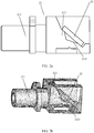
- FIG. 1a is a schematic diagram of an optical module packaged by means of the COB
- FIG. 1b is a schematic diagram of a commonly used molded plastic piece. As shown in FIG. 1a and FIG.
- a manner in which the optical module is packaged by means of the COB is directly fastening an optical chip (for example, a laser or a PD) on a printed circuit board (PCB) by using an integrally formed molded plastic piece, where two prisms are disposed in the molded plastic piece, light from a laser 102 is collimated by a lens 119 and then is turned horizontal by a reflection surface 111, and after travelling through a part of an optical path, a part of rays are reflected by a disposed clearance surface 113 to a monitor photodetector (MPD) for energy testing.
- MPD monitor photodetector
- Embodiments of the present invention provide an optical assembly and an optical module, so as to resolve a problem that when a COB technology is used for an optical module, a length of a molded plastic piece is caused to be relatively long because of an optical path, making it difficult to implement miniaturization of the optical module.
- a first aspect of the present invention provides an optical assembly, according to claim 1.
- the optical assembly comprises:
- a first lens and a second lens are further disposed in the light processing portion, where the first lens is disposed at a position from which the incident rays enter an optical path, and is configured to refract dispersed incident rays to parallel incident rays; and the second lens is disposed on an optical path that is obtained after reflection by the total reflection device, and is configured to focus the incident rays reflected by the total reflection device.
- the total reflection device includes a reflection sheet or a total reflection profile.
- an angle range of a first included angle between a reflective surface of the total reflection device and the incident rays is 30 degrees to 60 degrees.
- the first included angle is 45 degrees.
- an angle range of a second included angle between a plane on which the light splitting surface is located and the incident rays is 45 degrees to 90 degrees.
- the main body is in an integrally formed structure.
- a second aspect of the present invention provides an optical module, including: an optical module circuit, a substrate, and an optical assembly, where the optical module circuit includes a monitor photodetector MPD, and the optical module circuit and the optical assembly are disposed on the substrate; and the optical assembly includes a main body and a total reflection device, where the main body includes a fiber connection portion and a light processing portion, where the fiber connection portion is connected to the light processing portion, the fiber connection portion is connected to an external fiber, a light splitting surface is disposed in the light processing portion and is in contact with the total reflection device, the total reflection device is disposed in the light processing portion, and the light splitting surface is configured to reflect a part of incident rays to the MPD, and transmit the other part of the incident rays; and the total reflection device is configured to reflect, to the fiber connected to the fiber connection portion, the incident rays transmitted by the light splitting surface.
- a first lens and a second lens are further disposed in the light processing portion, where the first lens is disposed at a position from which the incident rays enter an optical path, and is configured to refract dispersed incident rays to parallel incident rays; and the second lens is disposed on an optical path that is obtained after reflection by the total reflection device, and is configured to focus the incident rays reflected by the total reflection device.
- the optical module circuit further includes a laser, where the laser is configured to generate the incident rays.
- the optical module circuit further includes a photodetector (PD), where the light splitting surface is configured to reflect received rays to the PD.
- PD photodetector
- a total reflection device is directly disposed in a light processing portion, and a light splitting surface is disposed to transmit a part of incident rays to the total reflection device, where the incident rays are reflected to a connected fiber by the total reflection device, and the light splitting surface may directly reflect a small part of the incident rays to an MPD for testing.
- an optical path is relatively short, and package can be performed by means of a COB, thereby decreasing a size of the optical assembly, and implementing miniaturization of the optical module to which the optical assembly is applied.
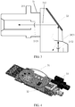
- FIG. 2a is a front view of a structure of Embodiment 1 of an optical assembly according to the present invention
- FIG. 2b is a 3D diagram of a structure of Embodiment 1 of an optical assembly according to the present invention. As shown in FIG. 2a and FIG.
- the optical assembly includes a main body 21 and a total reflection device 22, where the main body 21 includes a fiber connection portion 211 and a light processing portion 212, where the fiber connection portion 211 is connected to the light processing portion 212, and the fiber connection portion 211 is connected to an external fiber; a light splitting surface 2121 is disposed in the light processing portion 212, and is in contact with the total reflection device, where the light splitting surface 2121 is configured to reflect a part of incident rays to a monitor photodetector (English: Monitor Photo Detector, MPD for short), and transmit the other part of the incident rays; and the total reflection device 22 is disposed in the light processing portion 212, configured to reflect, to the fiber connected to the fiber connection portion 211, the incident rays transmitted by the light splitting surface 2121.
- a monitor photodetector International: Monitor Photo Detector, MPD for short
- the total reflection device 22 is disposed on the main body 21, so that incident rays can be reflected, and the light processing portion 212 is configured to process the incident rays.
- the light splitting surface 2121 is disposed by means of a Fresnel reflection effect of a sloping surface, and a smooth sloping surface, that is, the light splitting surface 2121, is formed in the light processing portion 212 of the main body 21 by hollowing an optical path along which the incident rays are input. Most incident rays may be transmitted by the sloping surface. Because of the intrinsic Fresnel reflection effect, a small part of the incident rays are reflected to the disposed MPD, and a photon-generated current is generated, which may reflect a value of an output optical power.
- both a key chip and optical chip (for example, a laser) are placed on a substrate, and then the optical assembly is packaged at a proper position by using a COB technology.
- a total reflection device is directly disposed in a light processing portion, and a light splitting surface is disposed to transmit a part of incident rays to the total reflection device, where the incident rays are reflected to a connected fiber by the total reflection device, and the light splitting surface may directly reflect a small part of the incident rays to an MPD for testing.
- an optical path is relatively short, and package can be performed by means of a COB, thereby decreasing a size of the optical assembly, and implementing miniaturization of an optical module to which the optical assembly is applied.
- FIG. 3 is a schematic sectional view of Embodiment 2 of an optical assembly not according to the present invention.
- a first lens 2122 and a second lens 2123 are further disposed in the light processing portion 212 of the optical assembly, where the first lens 2122 is disposed at a position from which the incident rays enter an optical path, and is configured to refract dispersed incident rays to parallel incident rays; and the second lens 2123 is disposed on an optical path that is obtained after reflection by the total reflection device 22, and is configured to focus the incident rays reflected by the total reflection device.
- the total reflection device 22 includes a reflection sheet or a total reflection profile, or may be another device having a total reflection function.
- an angle range of a first included angle between a reflective surface of the total reflection device and the incident rays is 30 degrees to 60 degrees. As long as the incident rays can be reflected to the fiber connected to the fiber connection portion, a specific value of the first included angle is not limited in this solution.
- the first included angle may be 45 degrees.
- the incident rays when the incident rays are input in a direction perpendicular to a horizontal direction in the figure, the incident rays are refracted by the first lens 2122 into parallel rays, and are transmitted by the light splitting surface 2121 to the reflective surface of the optical reflection device; if the first included angle is 45 degrees, the incident rays may be precisely reflected to the rayconnected to the ray connection portion 211 that is parallel to a horizontal plane.
- an angle range of a second included angle between a plane on which the light splitting surface 2121 is located and the incident rays is 45 degrees to 90 degrees. That is, as a position shown in FIG. 3 , an included angle between the light splitting surface 2121 and the horizontal plane is less than 45 degrees.
- a specific value of the second included angle is not limited in this application, as long as a small part of the incident rays that are reflected by the light splitting surface can be transmitted to the MPD.
- the main body is an injection molded part in an integrally formed structure.
- a transmit optical path when dispersed rays are input to a plastic molded part, the rays are turned into parallel rays by the first lens.
- most parallel rays are transmitted by the light splitting surface, and then are transmitted to the fiber after being reflected by the total reflection device and being focused once by the second lens.
- a small part of the incident rays that are not transmitted by the light splitting surface and are reflected by the light splitting surface are reflected to the MPD for testing, where the light splitting surface is disposed by means of a Fresnel reflection effect of a sloping surface. Because of the intrinsic Fresnel reflection effect, a small part of the rays are reflected to the MPD, and a photon-generated current is generated.
- a value of the current may reflect a value of an output optical power.
- a total reflection device is directly disposed in a light processing portion, and a light splitting surface is disposed to transmit a part of incident rays to the total reflection device, where the incident rays are reflected to a connected fiber by the total reflection device, and the light splitting surface may directly reflect a small part of the incident rays to an MPD for testing.
- an optical path is relatively short, and package can be performed by means of a COB, thereby decreasing a size of the optical assembly, and implementing miniaturization of an optical module to which the optical assembly is applied.
- a first lens and a second lens are disposed to focus rays, improving a processing effect of the rays.
- FIG. 4 is a schematic structural diagram of an Embodiment of an optical module according to the present invention.
- the optical module includes: an optical module circuit 31, a substrate 32, and an optical assembly 33, where the optical module circuit 31 includes an MPD, and the optical module circuit 31 and the optical assembly 33 are disposed on the substrate 32; and the optical assembly 33 includes a main body and a total reflection device, where the main body includes a fiber connection portion and a light processing portion, where the fiber connection portion is connected to the light processing portion, the fiber connection portion is connected to an external fiber, a light splitting surface is disposed in the light processing portion and is in contact with the total reflection device, and the total reflection device is disposed in the light processing portion, where if the optical assembly is applied to a transmit optical path, the light splitting surface is configured to reflect a part of incident rays to the MPD, and transmit the other part of the incident rays; and the total reflection device is configured to reflect, to the fiber connected to the fiber connection portion, the incident rays transmitted by the
- the light processing portion is configured to process the incident rays
- the optical assembly 33 is the optical assembly shown in FIG. 2 .
- a first lens and a second lens are further disposed in the light processing portion, where the first lens is disposed at a position from which the incident rays enter an optical path, and is configured to refract dispersed incident rays to parallel incident rays; and the second lens is disposed on an optical path that is obtained after reflection by the total reflection device, and is configured to focus the incident rays reflected by the total reflection device.
- the optical module circuit 31 further includes a laser, where the laser is configured to generate the incident rays.
- the substrate 32 which may be a PCB, a flexible substrate, a ceramic substrate, or an organic substrate.
- the optical assembly 33 in this application may be effectively applied to a pluggable module, and an application example of the pluggable module is a small form-factor pluggable (English: Small Form-factor Pluggable, SFP for short) optical module shown in FIG. 4 .
- the optical assembly 33 may be directly placed on a PCB in the SFP, and directly externally connected to an LC plug, and internally connected to the laser or a receiver chip.
- the laser and a driver or the receiver chip and a trans-impedance-amplifier (English: trans-impedance-amplifier, TIA for short)) in a transmit part are placed under the main body of the optical assembly and on the module PCB.
- a board on which the module is located inputs an electrical signal to the driver by using an electrical interface of the module, and the driver drives the laser after receiving the signal, so that the laser sends an optical signal.
- a path on a receive side is precisely reverse.
- an LC fiber sends an optical chip, which is transferred to the optical assembly part in this application, and separately output to the receiver chip in a photodetector (PD).
- PD photodetector
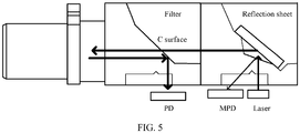
- FIG. 5 is a schematic diagram of an optical path in an embodiment of an optical module according to the present invention.
- the optical assembly 33 not only may be applied to a transmit optical path, but also may be applied to a receive optical path. If the optical assembly 33 is applied to the receive optical path, the optical module circuit further includes a PD, where the light splitting surface is configured to reflect received rays to the PD.
- the optical assembly may be further effectively applied to a module, for example, a cascaded wavelength multiplexing scenario.
- a module for example, a cascaded wavelength multiplexing scenario.
- transmitted rays and received rays have different wavelengths, and a filter is designed to perform transmission for one wavelength, and perform reflection for another wavelength, thereby implementing a BiDi transmission function.
- the rays are turned into parallel rays by a curved lens.
- the parallel rays are reflected by a reflection sheet, then are transmitted by the filter, and are input to a fiber after being focused once by a lens.
- the rays output by the fiber are reflected downward by the light splitting surface according to a total reflection effect, and are input to the PD after being focused once by the lens.
- optical assembly of this application includes a reverse design of receiving and transmission, for example, positions of the laser and the PD are exchanged, and the C surface is turned into a sloping surface, where a same principle is used.
- an improved optical module is applied to a transmit optical path or a receive optical path, a total reflection device is directly disposed in a light processing portion, and a light splitting surface is disposed to transmit a part of incident rays to the total reflection device, where the incident rays are reflected to a connected fiber by the total reflection device, and the light splitting surface may directly reflect a small part of the incident rays to an MPD for testing.
- an optical path is relatively short, and package can be performed by means of a COB, thereby decreasing a size of an optical assembly, and implementing miniaturization of the optical module to which the optical assembly is applied.
- a transmit optical power monitoring function is integrated, which can implement a module digital monitoring function, and can implement a wavelength division multiplexing function by means of multistage cascading.
Description
- Embodiments of the present invention relate to optoelectronic technologies, and in particular, to an optical assembly and an optical module.
- To keep up with the explosive growth of data services, optoelectronic interconnection modules of an enterprise network and a data center develop towards a trend of a higher speed and a higher density. In a case in which a unit bit rate of a photoelectric device is fully developed, an optical module for which parallel cables are used becomes a solution of further improving receiving and sending efficiency, for example, a protocol module such as a quad SFP (QSFP) interface based on a multiple-fiber push-on/pull-off (MPO) interface, and a 120 GB/s 12x Small Form-factor Pluggable (CXP) interface.
- For example,
US 2015/0086165A1 refers to an optical receptacle and optical module provided with the same. - Currently, a package technology commonly used for the optical module includes a transistor-outline can (TO-CAN) and a chip on board technology (COB).
FIG. 1a is a schematic diagram of an optical module packaged by means of the COB, andFIG. 1b is a schematic diagram of a commonly used molded plastic piece. As shown inFIG. 1a and FIG. 1b , a manner in which the optical module is packaged by means of the COB is directly fastening an optical chip (for example, a laser or a PD) on a printed circuit board (PCB) by using an integrally formed molded plastic piece, where two prisms are disposed in the molded plastic piece, light from alaser 102 is collimated by alens 119 and then is turned horizontal by areflection surface 111, and after travelling through a part of an optical path, a part of rays are reflected by a disposedclearance surface 113 to a monitor photodetector (MPD) for energy testing. In the manner, a clearance needs to be added to a design of the optical path, and a length of the optical path is relatively long. - However, when the molded plastic piece in the optical module is packaged by means of the COB, because the optical path is relatively long, a length of the molded plastic piece is caused to be relatively long, making it difficult to implement miniaturization of the optical module.
- Embodiments of the present invention provide an optical assembly and an optical module, so as to resolve a problem that when a COB technology is used for an optical module, a length of a molded plastic piece is caused to be relatively long because of an optical path, making it difficult to implement miniaturization of the optical module.
- A first aspect of the present invention provides an optical assembly, according to claim 1. The optical assembly comprises:
- a main body and a total reflection device, where
- the main body includes a fiber connection portion and a light processing portion, where the fiber connection portion is connected to the light processing portion;
- the fiber connection portion is connected to an external fiber; and
- a light splitting surface is disposed in the light processing portion and is in contact with the total reflection device, where the light splitting surface is configured to reflect a part of incident rays to a monitor photodetector MPD, and transmit the other part of the incident rays; and the total reflection device is disposed in the light processing portion, configured to reflect, to the fiber connected to the fiber connection portion, the incident rays transmitted by the light splitting surface.
- With reference to the first aspect, in a first possible implementation manner of the first aspect, a first lens and a second lens are further disposed in the light processing portion, where the first lens is disposed at a position from which the incident rays enter an optical path, and is configured to refract dispersed incident rays to parallel incident rays; and the second lens is disposed on an optical path that is obtained after reflection by the total reflection device, and is configured to focus the incident rays reflected by the total reflection device.
- With reference to the first aspect or the first possible implementation manner of the first aspect, in a second possible implementation manner of the first aspect, the total reflection device includes a reflection sheet or a total reflection profile.
- With reference to the second possible implementation manner of the first aspect, in a third possible implementation manner of the first aspect, an angle range of a first included angle between a reflective surface of the total reflection device and the incident rays is 30 degrees to 60 degrees.
- With reference to the third possible implementation manner of the first aspect, in a fourth possible implementation manner of the first aspect, the first included angle is 45 degrees.
- With reference to the first aspect or any one of the first to the fourth possible implementation manners of the first aspect, in a fifth possible implementation manner of the first aspect, an angle range of a second included angle between a plane on which the light splitting surface is located and the incident rays is 45 degrees to 90 degrees.
- With reference to the first aspect or any one of the first to the fifth possible implementation manners of the first aspect, in a sixth possible implementation manner of the first aspect, the main body is in an integrally formed structure.
- A second aspect of the present invention provides an optical module, including: an optical module circuit, a substrate, and an optical assembly, where the optical module circuit includes a monitor photodetector MPD, and the optical module circuit and the optical assembly are disposed on the substrate; and
the optical assembly includes a main body and a total reflection device, where the main body includes a fiber connection portion and a light processing portion, where the fiber connection portion is connected to the light processing portion, the fiber connection portion is connected to an external fiber, a light splitting surface is disposed in the light processing portion and is in contact with the total reflection device, the total reflection device is disposed in the light processing portion, and the light splitting surface is configured to reflect a part of incident rays to the MPD, and transmit the other part of the incident rays; and the total reflection device is configured to reflect, to the fiber connected to the fiber connection portion, the incident rays transmitted by the light splitting surface. - With reference to the second aspect, in a first possible implementation manner of the second aspect, a first lens and a second lens are further disposed in the light processing portion, where the first lens is disposed at a position from which the incident rays enter an optical path, and is configured to refract dispersed incident rays to parallel incident rays; and the second lens is disposed on an optical path that is obtained after reflection by the total reflection device, and is configured to focus the incident rays reflected by the total reflection device.
- With reference to the second aspect or the first possible implementation manner of the second aspect, in a second possible implementation manner of the second aspect, the optical module circuit further includes a laser, where the laser is configured to generate the incident rays.
- With reference to the second aspect or the first or the second possible implementation manner of the second aspect, in a third possible implementation manner of the second aspect, the optical module circuit further includes a photodetector (PD), where the light splitting surface is configured to reflect received rays to the PD.
- According to the optical assembly and the optical module provided in the present invention, a total reflection device is directly disposed in a light processing portion, and a light splitting surface is disposed to transmit a part of incident rays to the total reflection device, where the incident rays are reflected to a connected fiber by the total reflection device, and the light splitting surface may directly reflect a small part of the incident rays to an MPD for testing. In this way, an optical path is relatively short, and package can be performed by means of a COB, thereby
decreasing a size of the optical assembly, and implementing miniaturization of the optical module to which the optical assembly is applied. - To describe the technical solutions in the embodiments of the present invention or in the prior art more clearly, the following briefly introduces the accompanying drawings required for describing the embodiments or the prior art. Apparently, the accompanying drawings in the following description show some embodiments of the present invention, and persons of ordinary skill in the art may still derive other drawings from these accompanying drawings without creative efforts.
-
FIG. 1a is a schematic diagram of an optical module packaged by means of a COB; -
FIG. 1b is a schematic diagram of a commonly used molded plastic piece; -
FIG. 2a is a front view of a structure of Embodiment 1 of an optical assembly according to the present invention; -
FIG. 2b is a 3D diagram of a structure of Embodiment 1 of an optical assembly according to the present invention; -
FIG. 3 is a schematic sectional view of Embodiment 2 of an optical assembly not according to the present invention; -
FIG. 4 is a schematic structural diagram of Embodiment 1 of an optical module according to the present invention; and -
FIG. 5 is a schematic diagram of an optical path in an embodiment of an optical module according to the present invention. - To make the objectives, technical solutions, and advantages of the embodiments of the present invention clearer, the following clearly and completely describes the technical solutions in the embodiments of the present invention with reference to the accompanying drawings in the embodiments of the present invention. Apparently, the described embodiments are some but not all of the embodiments of the present invention. All other embodiments obtained by persons of ordinary skill in the art based on the embodiments of the present invention without creative efforts shall fall within the protection scope of the present invention.
-
FIG. 2a is a front view of a structure of Embodiment 1 of an optical assembly according to the present invention; andFIG. 2b is a 3D diagram of a structure of Embodiment 1 of an optical assembly according to the present invention. As shown inFIG. 2a and FIG. 2b , the optical assembly includes amain body 21 and atotal reflection device 22, where themain body 21 includes afiber connection portion 211 and alight processing portion 212, where thefiber connection portion 211 is connected to thelight processing portion 212, and thefiber connection portion 211 is connected to an external fiber; alight splitting surface 2121 is disposed in thelight processing portion 212, and is in contact with the total reflection device, where thelight splitting surface 2121 is configured to reflect a part of incident rays to a monitor photodetector (English: Monitor Photo Detector, MPD for short), and transmit the other part of the incident rays; and thetotal reflection device 22 is disposed in thelight processing portion 212, configured to reflect, to the fiber connected to thefiber connection portion 211, the incident rays transmitted by thelight splitting surface 2121. - In Embodiment 1, as shown in
FIG. 2a and FIG. 2b , thetotal reflection device 22 is disposed on themain body 21, so that incident rays can be reflected, and thelight processing portion 212 is configured to process the incident rays. Thelight splitting surface 2121 is disposed by means of a Fresnel reflection effect of a sloping surface, and a smooth sloping surface, that is, thelight splitting surface 2121, is formed in thelight processing portion 212 of themain body 21 by hollowing an optical path along which the incident rays are input. Most incident rays may be transmitted by the sloping surface. Because of the intrinsic Fresnel reflection effect, a small part of the incident rays are reflected to the disposed MPD, and a photon-generated current is generated, which may reflect a value of an output optical power. - When the optical assembly is applied, both a key chip and optical chip (for example, a laser) are placed on a substrate, and then the optical assembly is packaged at a proper position by using a COB technology.
- According to the optical assembly provided in Embodiment 1, a total reflection device is directly disposed in a light processing portion, and a light splitting surface is disposed to transmit a part of incident rays to the total reflection device, where the incident rays are reflected to a connected fiber by the total reflection device, and the light splitting surface may directly reflect a small part of the incident rays to an MPD for testing. In this way, an optical path is relatively short, and package can be performed by means of a COB, thereby decreasing a size of the optical assembly, and implementing miniaturization of an optical module to which the optical assembly is applied.
-
FIG. 3 is a schematic sectional view of Embodiment 2 of an optical assembly not according to the present invention. As shown inFIG. 3 , based onFIG. 2 , afirst lens 2122 and asecond lens 2123 are further disposed in thelight processing portion 212 of the optical assembly, where thefirst lens 2122 is disposed at a position from which the incident rays enter an optical path, and is configured to refract dispersed incident rays to parallel incident rays; and thesecond lens 2123 is disposed on an optical path that is obtained after reflection by thetotal reflection device 22, and is configured to focus the incident rays reflected by the total reflection device. - In Embodiment 2 the
total reflection device 22 includes a reflection sheet or a total reflection profile, or may be another device having a total reflection function. Generally, an angle range of a first included angle between a reflective surface of the total reflection device and the incident rays is 30 degrees to 60 degrees. As long as the incident rays can be reflected to the fiber connected to the fiber connection portion, a specific value of the first included angle is not limited in this solution. - Preferably, the first included angle may be 45 degrees. As shown in
FIG. 3 , when the incident rays are input in a direction perpendicular to a horizontal direction in the figure, the incident rays are refracted by thefirst lens 2122 into parallel rays, and are transmitted by thelight splitting surface 2121 to the reflective surface of the optical reflection device; if the first included angle is 45 degrees, the incident rays may be precisely reflected to the rayconnected to theray connection portion 211 that is parallel to a horizontal plane. - In addition, an angle range of a second included angle between a plane on which the
light splitting surface 2121 is located and the incident rays is 45 degrees to 90 degrees. That is, as a position shown inFIG. 3 , an included angle between thelight splitting surface 2121 and the horizontal plane is less than 45 degrees. A specific value of the second included angle is not limited in this application, as long as a small part of the incident rays that are reflected by the light splitting surface can be transmitted to the MPD. - In Embodiment 2, the main body is an injection molded part in an integrally formed structure.
- Similarly, using
FIG. 3 as an example, for a transmit optical path, when dispersed rays are input to a plastic molded part, the rays are turned into parallel rays by the first lens. When passing through the light splitting surface, most parallel rays are transmitted by the light splitting surface, and then are transmitted to the fiber after being reflected by the total reflection device and being focused once by the second lens. A small part of the incident rays that are not transmitted by the light splitting surface and are reflected by the light splitting surface are reflected to the MPD for testing, where the light splitting surface is disposed by means of a Fresnel reflection effect of a sloping surface. Because of the intrinsic Fresnel reflection effect, a small part of the rays are reflected to the MPD, and a photon-generated current is generated. A value of the current may reflect a value of an output optical power. - According to the optical assembly provided in Embodiment 2, a total reflection device is directly disposed in a light processing portion, and a light splitting surface is disposed to transmit a part of incident rays to the total reflection device, where the incident rays are reflected to a connected fiber by the total reflection device, and the light splitting surface may directly reflect a small part of the incident rays to an MPD for testing. In this way, an optical path is relatively short, and package can be performed by means of a COB, thereby decreasing a size of the optical assembly, and implementing miniaturization of an optical module to which the optical assembly is applied. In addition, a first lens and a second lens are disposed to focus rays, improving a processing effect of the rays.
-
FIG. 4 is a schematic structural diagram of an Embodiment of an optical module according to the present invention. As shown inFIG. 4 , the optical module includes: anoptical module circuit 31, asubstrate 32, and anoptical assembly 33, where theoptical module circuit 31 includes an MPD, and theoptical module circuit 31 and theoptical assembly 33 are disposed on thesubstrate 32; and
theoptical assembly 33 includes a main body and a total reflection device, where the main body includes a fiber connection portion and a light processing portion, where the fiber connection portion is connected to the light processing portion, the fiber connection portion is connected to an external fiber, a light splitting surface is disposed in the light processing portion and is in contact with the total reflection device, and the total reflection device is disposed in the light processing portion, where if the optical assembly is applied to a transmit optical path, the light splitting surface is configured to reflect a part of incident rays to the MPD, and transmit the other part of the incident rays; and the total reflection device is configured to reflect, to the fiber connected to the fiber connection portion, the incident rays transmitted by the light splitting surface. - In this embodiment, the light processing portion is configured to process the incident rays, and the
optical assembly 33 is the optical assembly shown inFIG. 2 . Specifically, a first lens and a second lens are further disposed in the light processing portion, where the first lens is disposed at a position from which the incident rays enter an optical path, and is configured to refract dispersed incident rays to parallel incident rays; and the second lens is disposed on an optical path that is obtained after reflection by the total reflection device, and is configured to focus the incident rays reflected by the total reflection device. - Optically, the
optical module circuit 31 further includes a laser, where the laser is configured to generate the incident rays. - In addition, all key chips are placed on the
substrate 32, which may be a PCB, a flexible substrate, a ceramic substrate, or an organic substrate. - The
optical assembly 33 in this application may be effectively applied to a pluggable module, and an application example of the pluggable module is a small form-factor pluggable (English: Small Form-factor Pluggable, SFP for short) optical module shown inFIG. 4 . Theoptical assembly 33 may be directly placed on a PCB in the SFP, and directly externally connected to an LC plug, and internally connected to the laser or a receiver chip. In this embodiment, the laser and a driver (or the receiver chip and a trans-impedance-amplifier (English: trans-impedance-amplifier, TIA for short)) in a transmit part are placed under the main body of the optical assembly and on the module PCB. Using the transmit part as an example, a board on which the module is located inputs an electrical signal to the driver by using an electrical interface of the module, and the driver drives the laser after receiving the signal, so that the laser sends an optical signal. A path on a receive side is precisely reverse. At an end of an optical transmission system, an LC fiber sends an optical chip, which is transferred to the optical assembly part in this application, and separately output to the receiver chip in a photodetector (PD). After being amplified by the TIA, a received chip is output to the electrical interface of the module, and is finally processed on the board on which the module is located. -
FIG. 5 is a schematic diagram of an optical path in an embodiment of an optical module according to the present invention. As shown inFIG. 5 , theoptical assembly 33 not only may be applied to a transmit optical path, but also may be applied to a receive optical path. If theoptical assembly 33 is applied to the receive optical path, the optical module circuit further includes a PD, where the light splitting surface is configured to reflect received rays to the PD. - Based on the foregoing embodiments, the optical assembly may be further effectively applied to a module, for example, a cascaded wavelength multiplexing scenario. Specifically, as shown in
FIG. 5 , transmitted rays and received rays have different wavelengths, and a filter is designed to perform transmission for one wavelength, and perform reflection for another wavelength, thereby implementing a BiDi transmission function. For example, in the figure, for the transmit optical path, when dispersed rays are input to the optical assembly, the rays are turned into parallel rays by a curved lens. The parallel rays are reflected by a reflection sheet, then are transmitted by the filter, and are input to a fiber after being focused once by a lens. - For the receive optical path, after light output from the fiber is collimated by the lens, due to a 45-degree included angle formed between the light splitting surface (that is, a C surface in the figure) and the horizontal plane, the rays output by the fiber are reflected downward by the light splitting surface according to a total reflection effect, and are input to the PD after being focused once by the lens.
- Application of the optical assembly of this application includes a reverse design of receiving and transmission, for example, positions of the laser and the PD are exchanged, and the C surface is turned into a sloping surface, where a same principle is used.
- According to the optical module provided in this embodiment, an improved optical module is applied to a transmit optical path or a receive optical path, a total reflection device is directly disposed in a light processing portion, and a light splitting surface is disposed to transmit a part of incident rays to the total reflection device, where the incident rays are reflected to a connected fiber by the total reflection device, and the light splitting surface may directly reflect a small part of the incident rays to an MPD for testing. In this way, an optical path is relatively short, and package can be performed by means of a COB, thereby decreasing a size of an optical assembly, and implementing miniaturization of the optical module to which the optical assembly is applied. In addition, a transmit optical power monitoring function is integrated, which can implement a module digital monitoring function, and can implement a wavelength division multiplexing function by means of multistage cascading.
- Finally, it should be noted that the foregoing embodiments are merely intended for describing the technical solutions of the present invention, but not for limiting the present invention. Although the present invention is described in detail with reference to the foregoing embodiments, persons of ordinary skill in the art should understand that they may still make modifications to the technical solutions described in the foregoing embodiments or make equivalent replacements to some or all technical features thereof, without departing from the scope of the technical solutions of the embodiments of the present invention.
Claims (11)
- An optical assembly, wherein the assembly comprises: a main body (21) and a total reflection device (22), wherein
the main body (21) comprises a fiber connection portion (211) and a light processing portion (212), wherein the fiber connection portion (211) is connected to the light processing portion (212);
the fiber connection portion (211) is connected to an external fiber; and
a light splitting surface (2121) is disposed in the light processing portion (212), wherein the light splitting surface (2121) is configured to reflect a part of incident rays to a monitor photodetector MPD, and transmit the other part of the incident rays; and the total reflection device (22) is disposed in the light processing portion (212), configured to reflect, to the fiber connected to the fiber connection portion (211), the incident rays transmitted by the light splitting surface (2121), characterized in that
the light splitting surface (2121) is in contact with the total reflection device (22). - The optical assembly according to claim 1, wherein a first lens and a second lens are further disposed in the light processing portion, wherein the first lens is disposed at a position from which the incident rays enter an optical path, and is configured to refract dispersed incident rays to parallel incident rays; and the second lens is disposed on an optical path that is obtained after reflection by the total reflection device, and is configured to focus the incident rays reflected by the total reflection device.
- The optical assembly according to claim 1 or 2, wherein the total reflection device comprises a reflection sheet or a total reflection profile.
- The optical assembly according to claim 3, wherein an angle range of a first included angle between a reflective surface of the total reflection device and the incident rays is 30 degrees to 60 degrees.
- The optical assembly according to claim 4, wherein the first included angle is 45 degrees.
- The optical assembly according to any one of claims 1 to 5, wherein an angle range of a second included angle between a plane on which the light splitting surface is located and the incident rays is 45 degrees to 90 degrees.
- The optical assembly according to any one of claims 1 to 6, wherein the main body is in an integrally formed structure.
- An optical module, wherein the module comprises: an optical module circuit, a substrate, and an optical assembly according to claim 1, wherein the optical module circuit comprises a monitor photodetector MPD, and the optical module circuit and the optical assembly are disposed on the substrate.
- The optical module according to claim 8, wherein a first lens and a second lens are further disposed in the light processing portion, wherein the first lens is disposed at a position from which the incident rays enter an optical path, and is configured to refract dispersed incident rays to parallel incident rays; and the second lens is disposed on an optical path that is obtained after reflection by the total reflection device, and is configured to focus the incident rays reflected by the total reflection device.
- The optical module according to claim 8 or 9, wherein the optical module circuit further comprises a laser, wherein the laser is configured to generate the incident rays.
- The optical module according to any one of claims 8 to 10, wherein the optical module circuit further comprises a photodetector PD, wherein the light splitting surface is configured to reflect received rays to the PD.
Applications Claiming Priority (1)
| Application Number | Priority Date | Filing Date | Title |
|---|---|---|---|
| CN201510364009.5A CN106324771B (en) | 2015-06-26 | 2015-06-26 | Optical module and optical module |
Publications (2)
| Publication Number | Publication Date |
|---|---|
| EP3109681A1 EP3109681A1 (en) | 2016-12-28 |
| EP3109681B1 true EP3109681B1 (en) | 2019-08-07 |
Family
ID=56235698
Family Applications (1)
| Application Number | Title | Priority Date | Filing Date |
|---|---|---|---|
| EP16176153.1A Active EP3109681B1 (en) | 2015-06-26 | 2016-06-24 | Optical assembly and optical module |
Country Status (2)
| Country | Link |
|---|---|
| EP (1) | EP3109681B1 (en) |
| CN (1) | CN106324771B (en) |
Families Citing this family (7)
| Publication number | Priority date | Publication date | Assignee | Title |
|---|---|---|---|---|
| CN107479149B (en) * | 2017-09-08 | 2019-06-21 | 峻立科技股份有限公司 | Optical element with monitoring light splitting path |
| WO2019173999A1 (en) * | 2018-03-15 | 2019-09-19 | 华为技术有限公司 | Optical transceiver component, optical module, and communication device |
| CN108919433B (en) * | 2018-07-12 | 2020-01-17 | 青岛海信宽带多媒体技术有限公司 | Optical module |
| US11025030B2 (en) | 2018-07-12 | 2021-06-01 | Hisense Broadband Multimedia Technologies Co., Ltd. | Optical module |
| CN109752802A (en) * | 2019-01-29 | 2019-05-14 | 武汉联特科技有限公司 | Multichannel wavelength division multiplexed light receiving unit and optical module |
| CN111856661A (en) * | 2019-04-30 | 2020-10-30 | 讯芯电子科技(中山)有限公司 | Optical communication module |
| CN112099159A (en) * | 2019-06-17 | 2020-12-18 | 青岛海信宽带多媒体技术有限公司 | Optical module |
Citations (1)
| Publication number | Priority date | Publication date | Assignee | Title |
|---|---|---|---|---|
| CN104597576A (en) * | 2015-01-19 | 2015-05-06 | 武汉锐奥特科技有限公司 | Optical injection molding structure for parallel optical modules and with emitted light power monitoring function |
Family Cites Families (7)
| Publication number | Priority date | Publication date | Assignee | Title |
|---|---|---|---|---|
| JP3941873B2 (en) * | 2001-09-14 | 2007-07-04 | インフィネオン テクノロジーズ アクチエンゲゼルシャフト | Transmission / reception arrangement for bi-directional optical data transmission |
| US6959133B2 (en) * | 2004-01-06 | 2005-10-25 | Agilent Technologies, Inc. | Optical coupling module and method for forming the same |
| US8503838B2 (en) * | 2010-09-15 | 2013-08-06 | Avago Technologies General Ip (Singapore) Pte. Ltd. | Two-part optical coupling system having an air gap therein for reflecting light to provide optical feedback for monitoring optical output power levels in an optical transmitter (TX) |
| JP2013200347A (en) * | 2012-03-23 | 2013-10-03 | Enplas Corp | Optical receptacle and optical module including the same |
| US20140226988A1 (en) * | 2013-02-12 | 2014-08-14 | Avago Technologies General Ip (Singapore) Pte. Ltd | Bidirectional optical data communications module having reflective lens |
| CN203786342U (en) * | 2014-04-11 | 2014-08-20 | 苏州旭创科技有限公司 | Optical assembly |
| CN104238027A (en) * | 2014-09-11 | 2014-12-24 | 武汉电信器件有限公司 | Array element of beam splitting lens |
-
2015
- 2015-06-26 CN CN201510364009.5A patent/CN106324771B/en active Active
-
2016
- 2016-06-24 EP EP16176153.1A patent/EP3109681B1/en active Active
Patent Citations (1)
| Publication number | Priority date | Publication date | Assignee | Title |
|---|---|---|---|---|
| CN104597576A (en) * | 2015-01-19 | 2015-05-06 | 武汉锐奥特科技有限公司 | Optical injection molding structure for parallel optical modules and with emitted light power monitoring function |
Also Published As
| Publication number | Publication date |
|---|---|
| EP3109681A1 (en) | 2016-12-28 |
| CN106324771A (en) | 2017-01-11 |
| CN106324771B (en) | 2019-03-05 |
Similar Documents
| Publication | Publication Date | Title |
|---|---|---|
| EP3109681B1 (en) | Optical assembly and optical module | |
| US7539367B2 (en) | Optical system connection structure, optical component, and optical communication module | |
| US7399125B1 (en) | Lens array with integrated folding mirror | |
| JP4983703B2 (en) | Optical transmission system | |
| US9784919B2 (en) | Wavelength division multiplexing and demultiplexing transistor outline (TO)-can assemblies for use in optical communications, and methods | |
| US20120219256A1 (en) | Optical beam splitter for use in an optoelectronic module, and a method for performing optical beam splitting in an optoelectronic module | |
| TWI497142B (en) | Optical fiber connector | |
| KR950014912A (en) | Optical module for two-way transmission | |
| US9020308B2 (en) | Multi-channel optical module with polyhedral mirror | |
| US9733438B2 (en) | Optical connector for data transceiver modules and lens block for optical connectors | |
| JP2016009187A (en) | Parallel optical transceiver with top lens and bottom lens | |
| EP3425436A1 (en) | Optical receptacle, optical module, and method for manufacturing optical module | |
| US20130177320A1 (en) | Multi-laser transmitter optical subassembly for optoelectronic modules | |
| US20160047989A1 (en) | Wavelength division multiplexing of uncooled lasers with wavelength-common dispersive element | |
| CN111061019A (en) | Optical module | |
| US9046667B2 (en) | Photoelectric conversion device and optical fiber coupling connector | |
| CN104678517B (en) | A kind of integrated semiconductor optical device | |
| US9385829B2 (en) | Optical transceiver having optics with rotated optical path | |
| Hsiao et al. | Compact and passive-alignment 4-channel× 2.5-Gbps optical interconnect modules based on silicon optical benches with 45 micro-reflectors | |
| US9448373B2 (en) | Opto-electronic micro-module and method for forming the same | |
| KR101723135B1 (en) | Bi-directional optical module | |
| US9423581B2 (en) | Parallel optical system with integrated monitoring photodetectors | |
| US9395503B2 (en) | Optical-electric coupling element and optical connector using same | |
| KR101416638B1 (en) | Monitoring device for optical signal in planar light wave circuits | |
| US9851516B2 (en) | Optical components assembly |
Legal Events
| Date | Code | Title | Description |
|---|---|---|---|
| PUAI | Public reference made under article 153(3) epc to a published international application that has entered the european phase |
Free format text: ORIGINAL CODE: 0009012 |
|
| STAA | Information on the status of an ep patent application or granted ep patent |
Free format text: STATUS: REQUEST FOR EXAMINATION WAS MADE |
|
| 17P | Request for examination filed |
Effective date: 20160624 |
|
| AK | Designated contracting states |
Kind code of ref document: A1 Designated state(s): AL AT BE BG CH CY CZ DE DK EE ES FI FR GB GR HR HU IE IS IT LI LT LU LV MC MK MT NL NO PL PT RO RS SE SI SK SM TR |
|
| AX | Request for extension of the european patent |
Extension state: BA ME |
|
| GRAP | Despatch of communication of intention to grant a patent |
Free format text: ORIGINAL CODE: EPIDOSNIGR1 |
|
| RIC1 | Information provided on ipc code assigned before grant |
Ipc: G02B 6/42 20060101AFI20181031BHEP Ipc: G02B 6/293 20060101ALN20181031BHEP |
|
| STAA | Information on the status of an ep patent application or granted ep patent |
Free format text: STATUS: GRANT OF PATENT IS INTENDED |
|
| INTG | Intention to grant announced |
Effective date: 20181206 |
|
| GRAS | Grant fee paid |
Free format text: ORIGINAL CODE: EPIDOSNIGR3 |
|
| GRAJ | Information related to disapproval of communication of intention to grant by the applicant or resumption of examination proceedings by the epo deleted |
Free format text: ORIGINAL CODE: EPIDOSDIGR1 |
|
| GRAL | Information related to payment of fee for publishing/printing deleted |
Free format text: ORIGINAL CODE: EPIDOSDIGR3 |
|
| STAA | Information on the status of an ep patent application or granted ep patent |
Free format text: STATUS: REQUEST FOR EXAMINATION WAS MADE |
|
| GRAR | Information related to intention to grant a patent recorded |
Free format text: ORIGINAL CODE: EPIDOSNIGR71 |
|
| STAA | Information on the status of an ep patent application or granted ep patent |
Free format text: STATUS: GRANT OF PATENT IS INTENDED |
|
| INTC | Intention to grant announced (deleted) | ||
| RIC1 | Information provided on ipc code assigned before grant |
Ipc: G02B 6/42 20060101AFI20190510BHEP Ipc: G02B 6/293 20060101ALN20190510BHEP |
|
| INTG | Intention to grant announced |
Effective date: 20190523 |
|
| RIN1 | Information on inventor provided before grant (corrected) |
Inventor name: HU, CHIHAO Inventor name: HU, RUI Inventor name: ZHOU, CHUANG |
|
| GRAA | (expected) grant |
Free format text: ORIGINAL CODE: 0009210 |
|
| STAA | Information on the status of an ep patent application or granted ep patent |
Free format text: STATUS: THE PATENT HAS BEEN GRANTED |
|
| AK | Designated contracting states |
Kind code of ref document: B1 Designated state(s): AL AT BE BG CH CY CZ DE DK EE ES FI FR GB GR HR HU IE IS IT LI LT LU LV MC MK MT NL NO PL PT RO RS SE SI SK SM TR |
|
| REG | Reference to a national code |
Ref country code: GB Ref legal event code: FG4D |
|
| REG | Reference to a national code |
Ref country code: CH Ref legal event code: EP Ref country code: AT Ref legal event code: REF Ref document number: 1164721 Country of ref document: AT Kind code of ref document: T Effective date: 20190815 |
|
| REG | Reference to a national code |
Ref country code: DE Ref legal event code: R096 Ref document number: 602016017984 Country of ref document: DE |
|
| REG | Reference to a national code |
Ref country code: IE Ref legal event code: FG4D |
|
| REG | Reference to a national code |
Ref country code: NL Ref legal event code: MP Effective date: 20190807 |
|
| REG | Reference to a national code |
Ref country code: LT Ref legal event code: MG4D |
|
| PG25 | Lapsed in a contracting state [announced via postgrant information from national office to epo] |
Ref country code: PT Free format text: LAPSE BECAUSE OF FAILURE TO SUBMIT A TRANSLATION OF THE DESCRIPTION OR TO PAY THE FEE WITHIN THE PRESCRIBED TIME-LIMIT Effective date: 20191209 Ref country code: BG Free format text: LAPSE BECAUSE OF FAILURE TO SUBMIT A TRANSLATION OF THE DESCRIPTION OR TO PAY THE FEE WITHIN THE PRESCRIBED TIME-LIMIT Effective date: 20191107 Ref country code: NL Free format text: LAPSE BECAUSE OF FAILURE TO SUBMIT A TRANSLATION OF THE DESCRIPTION OR TO PAY THE FEE WITHIN THE PRESCRIBED TIME-LIMIT Effective date: 20190807 Ref country code: LT Free format text: LAPSE BECAUSE OF FAILURE TO SUBMIT A TRANSLATION OF THE DESCRIPTION OR TO PAY THE FEE WITHIN THE PRESCRIBED TIME-LIMIT Effective date: 20190807 Ref country code: HR Free format text: LAPSE BECAUSE OF FAILURE TO SUBMIT A TRANSLATION OF THE DESCRIPTION OR TO PAY THE FEE WITHIN THE PRESCRIBED TIME-LIMIT Effective date: 20190807 Ref country code: SE Free format text: LAPSE BECAUSE OF FAILURE TO SUBMIT A TRANSLATION OF THE DESCRIPTION OR TO PAY THE FEE WITHIN THE PRESCRIBED TIME-LIMIT Effective date: 20190807 Ref country code: NO Free format text: LAPSE BECAUSE OF FAILURE TO SUBMIT A TRANSLATION OF THE DESCRIPTION OR TO PAY THE FEE WITHIN THE PRESCRIBED TIME-LIMIT Effective date: 20191107 Ref country code: FI Free format text: LAPSE BECAUSE OF FAILURE TO SUBMIT A TRANSLATION OF THE DESCRIPTION OR TO PAY THE FEE WITHIN THE PRESCRIBED TIME-LIMIT Effective date: 20190807 |
|
| REG | Reference to a national code |
Ref country code: AT Ref legal event code: MK05 Ref document number: 1164721 Country of ref document: AT Kind code of ref document: T Effective date: 20190807 |
|
| PG25 | Lapsed in a contracting state [announced via postgrant information from national office to epo] |
Ref country code: ES Free format text: LAPSE BECAUSE OF FAILURE TO SUBMIT A TRANSLATION OF THE DESCRIPTION OR TO PAY THE FEE WITHIN THE PRESCRIBED TIME-LIMIT Effective date: 20190807 Ref country code: GR Free format text: LAPSE BECAUSE OF FAILURE TO SUBMIT A TRANSLATION OF THE DESCRIPTION OR TO PAY THE FEE WITHIN THE PRESCRIBED TIME-LIMIT Effective date: 20191108 Ref country code: IS Free format text: LAPSE BECAUSE OF FAILURE TO SUBMIT A TRANSLATION OF THE DESCRIPTION OR TO PAY THE FEE WITHIN THE PRESCRIBED TIME-LIMIT Effective date: 20191207 Ref country code: RS Free format text: LAPSE BECAUSE OF FAILURE TO SUBMIT A TRANSLATION OF THE DESCRIPTION OR TO PAY THE FEE WITHIN THE PRESCRIBED TIME-LIMIT Effective date: 20190807 Ref country code: LV Free format text: LAPSE BECAUSE OF FAILURE TO SUBMIT A TRANSLATION OF THE DESCRIPTION OR TO PAY THE FEE WITHIN THE PRESCRIBED TIME-LIMIT Effective date: 20190807 Ref country code: AL Free format text: LAPSE BECAUSE OF FAILURE TO SUBMIT A TRANSLATION OF THE DESCRIPTION OR TO PAY THE FEE WITHIN THE PRESCRIBED TIME-LIMIT Effective date: 20190807 |
|
| PG25 | Lapsed in a contracting state [announced via postgrant information from national office to epo] |
Ref country code: TR Free format text: LAPSE BECAUSE OF FAILURE TO SUBMIT A TRANSLATION OF THE DESCRIPTION OR TO PAY THE FEE WITHIN THE PRESCRIBED TIME-LIMIT Effective date: 20190807 |
|
| PG25 | Lapsed in a contracting state [announced via postgrant information from national office to epo] |
Ref country code: RO Free format text: LAPSE BECAUSE OF FAILURE TO SUBMIT A TRANSLATION OF THE DESCRIPTION OR TO PAY THE FEE WITHIN THE PRESCRIBED TIME-LIMIT Effective date: 20190807 Ref country code: IT Free format text: LAPSE BECAUSE OF FAILURE TO SUBMIT A TRANSLATION OF THE DESCRIPTION OR TO PAY THE FEE WITHIN THE PRESCRIBED TIME-LIMIT Effective date: 20190807 Ref country code: EE Free format text: LAPSE BECAUSE OF FAILURE TO SUBMIT A TRANSLATION OF THE DESCRIPTION OR TO PAY THE FEE WITHIN THE PRESCRIBED TIME-LIMIT Effective date: 20190807 Ref country code: AT Free format text: LAPSE BECAUSE OF FAILURE TO SUBMIT A TRANSLATION OF THE DESCRIPTION OR TO PAY THE FEE WITHIN THE PRESCRIBED TIME-LIMIT Effective date: 20190807 Ref country code: PL Free format text: LAPSE BECAUSE OF FAILURE TO SUBMIT A TRANSLATION OF THE DESCRIPTION OR TO PAY THE FEE WITHIN THE PRESCRIBED TIME-LIMIT Effective date: 20190807 Ref country code: DK Free format text: LAPSE BECAUSE OF FAILURE TO SUBMIT A TRANSLATION OF THE DESCRIPTION OR TO PAY THE FEE WITHIN THE PRESCRIBED TIME-LIMIT Effective date: 20190807 |
|
| PG25 | Lapsed in a contracting state [announced via postgrant information from national office to epo] |
Ref country code: SK Free format text: LAPSE BECAUSE OF FAILURE TO SUBMIT A TRANSLATION OF THE DESCRIPTION OR TO PAY THE FEE WITHIN THE PRESCRIBED TIME-LIMIT Effective date: 20190807 Ref country code: SM Free format text: LAPSE BECAUSE OF FAILURE TO SUBMIT A TRANSLATION OF THE DESCRIPTION OR TO PAY THE FEE WITHIN THE PRESCRIBED TIME-LIMIT Effective date: 20190807 Ref country code: IS Free format text: LAPSE BECAUSE OF FAILURE TO SUBMIT A TRANSLATION OF THE DESCRIPTION OR TO PAY THE FEE WITHIN THE PRESCRIBED TIME-LIMIT Effective date: 20200224 Ref country code: CZ Free format text: LAPSE BECAUSE OF FAILURE TO SUBMIT A TRANSLATION OF THE DESCRIPTION OR TO PAY THE FEE WITHIN THE PRESCRIBED TIME-LIMIT Effective date: 20190807 |
|
| REG | Reference to a national code |
Ref country code: DE Ref legal event code: R097 Ref document number: 602016017984 Country of ref document: DE |
|
| PLBE | No opposition filed within time limit |
Free format text: ORIGINAL CODE: 0009261 |
|
| STAA | Information on the status of an ep patent application or granted ep patent |
Free format text: STATUS: NO OPPOSITION FILED WITHIN TIME LIMIT |
|
| PG2D | Information on lapse in contracting state deleted |
Ref country code: IS |
|
| 26N | No opposition filed |
Effective date: 20200603 |
|
| PG25 | Lapsed in a contracting state [announced via postgrant information from national office to epo] |
Ref country code: SI Free format text: LAPSE BECAUSE OF FAILURE TO SUBMIT A TRANSLATION OF THE DESCRIPTION OR TO PAY THE FEE WITHIN THE PRESCRIBED TIME-LIMIT Effective date: 20190807 |
|
| PG25 | Lapsed in a contracting state [announced via postgrant information from national office to epo] |
Ref country code: MC Free format text: LAPSE BECAUSE OF FAILURE TO SUBMIT A TRANSLATION OF THE DESCRIPTION OR TO PAY THE FEE WITHIN THE PRESCRIBED TIME-LIMIT Effective date: 20190807 |
|
| REG | Reference to a national code |
Ref country code: CH Ref legal event code: PL |
|
| PG25 | Lapsed in a contracting state [announced via postgrant information from national office to epo] |
Ref country code: LU Free format text: LAPSE BECAUSE OF NON-PAYMENT OF DUE FEES Effective date: 20200624 |
|
| REG | Reference to a national code |
Ref country code: BE Ref legal event code: MM Effective date: 20200630 |
|
| PG25 | Lapsed in a contracting state [announced via postgrant information from national office to epo] |
Ref country code: CH Free format text: LAPSE BECAUSE OF NON-PAYMENT OF DUE FEES Effective date: 20200630 Ref country code: LI Free format text: LAPSE BECAUSE OF NON-PAYMENT OF DUE FEES Effective date: 20200630 Ref country code: IE Free format text: LAPSE BECAUSE OF NON-PAYMENT OF DUE FEES Effective date: 20200624 |
|
| PG25 | Lapsed in a contracting state [announced via postgrant information from national office to epo] |
Ref country code: BE Free format text: LAPSE BECAUSE OF NON-PAYMENT OF DUE FEES Effective date: 20200630 |
|
| PG25 | Lapsed in a contracting state [announced via postgrant information from national office to epo] |
Ref country code: MT Free format text: LAPSE BECAUSE OF FAILURE TO SUBMIT A TRANSLATION OF THE DESCRIPTION OR TO PAY THE FEE WITHIN THE PRESCRIBED TIME-LIMIT Effective date: 20190807 Ref country code: CY Free format text: LAPSE BECAUSE OF FAILURE TO SUBMIT A TRANSLATION OF THE DESCRIPTION OR TO PAY THE FEE WITHIN THE PRESCRIBED TIME-LIMIT Effective date: 20190807 |
|
| PG25 | Lapsed in a contracting state [announced via postgrant information from national office to epo] |
Ref country code: MK Free format text: LAPSE BECAUSE OF FAILURE TO SUBMIT A TRANSLATION OF THE DESCRIPTION OR TO PAY THE FEE WITHIN THE PRESCRIBED TIME-LIMIT Effective date: 20190807 |
|
| PGFP | Annual fee paid to national office [announced via postgrant information from national office to epo] |
Ref country code: FR Payment date: 20230510 Year of fee payment: 8 Ref country code: DE Payment date: 20230502 Year of fee payment: 8 |
|
| PGFP | Annual fee paid to national office [announced via postgrant information from national office to epo] |
Ref country code: GB Payment date: 20230504 Year of fee payment: 8 |