EP3109289A1 - Sealing tape, phosphor sheet, lighting equipment, liquid crystal display, method for manufacturing phosphor sheet, and sealing method - Google Patents
Sealing tape, phosphor sheet, lighting equipment, liquid crystal display, method for manufacturing phosphor sheet, and sealing method Download PDFInfo
- Publication number
- EP3109289A1 EP3109289A1 EP15752725.0A EP15752725A EP3109289A1 EP 3109289 A1 EP3109289 A1 EP 3109289A1 EP 15752725 A EP15752725 A EP 15752725A EP 3109289 A1 EP3109289 A1 EP 3109289A1
- Authority
- EP
- European Patent Office
- Prior art keywords
- layer
- phosphor
- sealing tape
- water vapor
- phosphor sheet
- Prior art date
- Legal status (The legal status is an assumption and is not a legal conclusion. Google has not performed a legal analysis and makes no representation as to the accuracy of the status listed.)
- Granted
Links
Images








Classifications
-
- B—PERFORMING OPERATIONS; TRANSPORTING
- B32—LAYERED PRODUCTS
- B32B—LAYERED PRODUCTS, i.e. PRODUCTS BUILT-UP OF STRATA OF FLAT OR NON-FLAT, e.g. CELLULAR OR HONEYCOMB, FORM
- B32B3/00—Layered products comprising a layer with external or internal discontinuities or unevennesses, or a layer of non-planar shape; Layered products comprising a layer having particular features of form
- B32B3/26—Layered products comprising a layer with external or internal discontinuities or unevennesses, or a layer of non-planar shape; Layered products comprising a layer having particular features of form characterised by a particular shape of the outline of the cross-section of a continuous layer; characterised by a layer with cavities or internal voids ; characterised by an apertured layer
-
- B—PERFORMING OPERATIONS; TRANSPORTING
- B32—LAYERED PRODUCTS
- B32B—LAYERED PRODUCTS, i.e. PRODUCTS BUILT-UP OF STRATA OF FLAT OR NON-FLAT, e.g. CELLULAR OR HONEYCOMB, FORM
- B32B15/00—Layered products comprising a layer of metal
- B32B15/04—Layered products comprising a layer of metal comprising metal as the main or only constituent of a layer, which is next to another layer of the same or of a different material
-
- B—PERFORMING OPERATIONS; TRANSPORTING
- B32—LAYERED PRODUCTS
- B32B—LAYERED PRODUCTS, i.e. PRODUCTS BUILT-UP OF STRATA OF FLAT OR NON-FLAT, e.g. CELLULAR OR HONEYCOMB, FORM
- B32B15/00—Layered products comprising a layer of metal
- B32B15/04—Layered products comprising a layer of metal comprising metal as the main or only constituent of a layer, which is next to another layer of the same or of a different material
- B32B15/08—Layered products comprising a layer of metal comprising metal as the main or only constituent of a layer, which is next to another layer of the same or of a different material of synthetic resin
-
- B—PERFORMING OPERATIONS; TRANSPORTING
- B32—LAYERED PRODUCTS
- B32B—LAYERED PRODUCTS, i.e. PRODUCTS BUILT-UP OF STRATA OF FLAT OR NON-FLAT, e.g. CELLULAR OR HONEYCOMB, FORM
- B32B15/00—Layered products comprising a layer of metal
- B32B15/04—Layered products comprising a layer of metal comprising metal as the main or only constituent of a layer, which is next to another layer of the same or of a different material
- B32B15/08—Layered products comprising a layer of metal comprising metal as the main or only constituent of a layer, which is next to another layer of the same or of a different material of synthetic resin
- B32B15/09—Layered products comprising a layer of metal comprising metal as the main or only constituent of a layer, which is next to another layer of the same or of a different material of synthetic resin comprising polyesters
-
- B—PERFORMING OPERATIONS; TRANSPORTING
- B32—LAYERED PRODUCTS
- B32B—LAYERED PRODUCTS, i.e. PRODUCTS BUILT-UP OF STRATA OF FLAT OR NON-FLAT, e.g. CELLULAR OR HONEYCOMB, FORM
- B32B15/00—Layered products comprising a layer of metal
- B32B15/20—Layered products comprising a layer of metal comprising aluminium or copper
-
- B—PERFORMING OPERATIONS; TRANSPORTING
- B32—LAYERED PRODUCTS
- B32B—LAYERED PRODUCTS, i.e. PRODUCTS BUILT-UP OF STRATA OF FLAT OR NON-FLAT, e.g. CELLULAR OR HONEYCOMB, FORM
- B32B27/00—Layered products comprising a layer of synthetic resin
- B32B27/06—Layered products comprising a layer of synthetic resin as the main or only constituent of a layer, which is next to another layer of the same or of a different material
-
- B—PERFORMING OPERATIONS; TRANSPORTING
- B32—LAYERED PRODUCTS
- B32B—LAYERED PRODUCTS, i.e. PRODUCTS BUILT-UP OF STRATA OF FLAT OR NON-FLAT, e.g. CELLULAR OR HONEYCOMB, FORM
- B32B27/00—Layered products comprising a layer of synthetic resin
- B32B27/06—Layered products comprising a layer of synthetic resin as the main or only constituent of a layer, which is next to another layer of the same or of a different material
- B32B27/08—Layered products comprising a layer of synthetic resin as the main or only constituent of a layer, which is next to another layer of the same or of a different material of synthetic resin
-
- B—PERFORMING OPERATIONS; TRANSPORTING
- B32—LAYERED PRODUCTS
- B32B—LAYERED PRODUCTS, i.e. PRODUCTS BUILT-UP OF STRATA OF FLAT OR NON-FLAT, e.g. CELLULAR OR HONEYCOMB, FORM
- B32B27/00—Layered products comprising a layer of synthetic resin
- B32B27/18—Layered products comprising a layer of synthetic resin characterised by the use of special additives
-
- B—PERFORMING OPERATIONS; TRANSPORTING
- B32—LAYERED PRODUCTS
- B32B—LAYERED PRODUCTS, i.e. PRODUCTS BUILT-UP OF STRATA OF FLAT OR NON-FLAT, e.g. CELLULAR OR HONEYCOMB, FORM
- B32B27/00—Layered products comprising a layer of synthetic resin
- B32B27/18—Layered products comprising a layer of synthetic resin characterised by the use of special additives
- B32B27/20—Layered products comprising a layer of synthetic resin characterised by the use of special additives using fillers, pigments, thixotroping agents
-
- B—PERFORMING OPERATIONS; TRANSPORTING
- B32—LAYERED PRODUCTS
- B32B—LAYERED PRODUCTS, i.e. PRODUCTS BUILT-UP OF STRATA OF FLAT OR NON-FLAT, e.g. CELLULAR OR HONEYCOMB, FORM
- B32B27/00—Layered products comprising a layer of synthetic resin
- B32B27/28—Layered products comprising a layer of synthetic resin comprising synthetic resins not wholly covered by any one of the sub-groups B32B27/30 - B32B27/42
-
- B—PERFORMING OPERATIONS; TRANSPORTING
- B32—LAYERED PRODUCTS
- B32B—LAYERED PRODUCTS, i.e. PRODUCTS BUILT-UP OF STRATA OF FLAT OR NON-FLAT, e.g. CELLULAR OR HONEYCOMB, FORM
- B32B27/00—Layered products comprising a layer of synthetic resin
- B32B27/28—Layered products comprising a layer of synthetic resin comprising synthetic resins not wholly covered by any one of the sub-groups B32B27/30 - B32B27/42
- B32B27/286—Layered products comprising a layer of synthetic resin comprising synthetic resins not wholly covered by any one of the sub-groups B32B27/30 - B32B27/42 comprising polysulphones; polysulfides
-
- B—PERFORMING OPERATIONS; TRANSPORTING
- B32—LAYERED PRODUCTS
- B32B—LAYERED PRODUCTS, i.e. PRODUCTS BUILT-UP OF STRATA OF FLAT OR NON-FLAT, e.g. CELLULAR OR HONEYCOMB, FORM
- B32B27/00—Layered products comprising a layer of synthetic resin
- B32B27/28—Layered products comprising a layer of synthetic resin comprising synthetic resins not wholly covered by any one of the sub-groups B32B27/30 - B32B27/42
- B32B27/288—Layered products comprising a layer of synthetic resin comprising synthetic resins not wholly covered by any one of the sub-groups B32B27/30 - B32B27/42 comprising polyketones
-
- B—PERFORMING OPERATIONS; TRANSPORTING
- B32—LAYERED PRODUCTS
- B32B—LAYERED PRODUCTS, i.e. PRODUCTS BUILT-UP OF STRATA OF FLAT OR NON-FLAT, e.g. CELLULAR OR HONEYCOMB, FORM
- B32B27/00—Layered products comprising a layer of synthetic resin
- B32B27/30—Layered products comprising a layer of synthetic resin comprising vinyl (co)polymers; comprising acrylic (co)polymers
-
- B—PERFORMING OPERATIONS; TRANSPORTING
- B32—LAYERED PRODUCTS
- B32B—LAYERED PRODUCTS, i.e. PRODUCTS BUILT-UP OF STRATA OF FLAT OR NON-FLAT, e.g. CELLULAR OR HONEYCOMB, FORM
- B32B27/00—Layered products comprising a layer of synthetic resin
- B32B27/30—Layered products comprising a layer of synthetic resin comprising vinyl (co)polymers; comprising acrylic (co)polymers
- B32B27/308—Layered products comprising a layer of synthetic resin comprising vinyl (co)polymers; comprising acrylic (co)polymers comprising acrylic (co)polymers
-
- B—PERFORMING OPERATIONS; TRANSPORTING
- B32—LAYERED PRODUCTS
- B32B—LAYERED PRODUCTS, i.e. PRODUCTS BUILT-UP OF STRATA OF FLAT OR NON-FLAT, e.g. CELLULAR OR HONEYCOMB, FORM
- B32B27/00—Layered products comprising a layer of synthetic resin
- B32B27/32—Layered products comprising a layer of synthetic resin comprising polyolefins
-
- B—PERFORMING OPERATIONS; TRANSPORTING
- B32—LAYERED PRODUCTS
- B32B—LAYERED PRODUCTS, i.e. PRODUCTS BUILT-UP OF STRATA OF FLAT OR NON-FLAT, e.g. CELLULAR OR HONEYCOMB, FORM
- B32B27/00—Layered products comprising a layer of synthetic resin
- B32B27/36—Layered products comprising a layer of synthetic resin comprising polyesters
-
- B—PERFORMING OPERATIONS; TRANSPORTING
- B32—LAYERED PRODUCTS
- B32B—LAYERED PRODUCTS, i.e. PRODUCTS BUILT-UP OF STRATA OF FLAT OR NON-FLAT, e.g. CELLULAR OR HONEYCOMB, FORM
- B32B3/00—Layered products comprising a layer with external or internal discontinuities or unevennesses, or a layer of non-planar shape; Layered products comprising a layer having particular features of form
- B32B3/26—Layered products comprising a layer with external or internal discontinuities or unevennesses, or a layer of non-planar shape; Layered products comprising a layer having particular features of form characterised by a particular shape of the outline of the cross-section of a continuous layer; characterised by a layer with cavities or internal voids ; characterised by an apertured layer
- B32B3/266—Layered products comprising a layer with external or internal discontinuities or unevennesses, or a layer of non-planar shape; Layered products comprising a layer having particular features of form characterised by a particular shape of the outline of the cross-section of a continuous layer; characterised by a layer with cavities or internal voids ; characterised by an apertured layer characterised by an apertured layer, the apertures going through the whole thickness of the layer, e.g. expanded metal, perforated layer, slit layer regular cells B32B3/12
-
- B—PERFORMING OPERATIONS; TRANSPORTING
- B32—LAYERED PRODUCTS
- B32B—LAYERED PRODUCTS, i.e. PRODUCTS BUILT-UP OF STRATA OF FLAT OR NON-FLAT, e.g. CELLULAR OR HONEYCOMB, FORM
- B32B3/00—Layered products comprising a layer with external or internal discontinuities or unevennesses, or a layer of non-planar shape; Layered products comprising a layer having particular features of form
- B32B3/26—Layered products comprising a layer with external or internal discontinuities or unevennesses, or a layer of non-planar shape; Layered products comprising a layer having particular features of form characterised by a particular shape of the outline of the cross-section of a continuous layer; characterised by a layer with cavities or internal voids ; characterised by an apertured layer
- B32B3/30—Layered products comprising a layer with external or internal discontinuities or unevennesses, or a layer of non-planar shape; Layered products comprising a layer having particular features of form characterised by a particular shape of the outline of the cross-section of a continuous layer; characterised by a layer with cavities or internal voids ; characterised by an apertured layer characterised by a layer formed with recesses or projections, e.g. hollows, grooves, protuberances, ribs
-
- B—PERFORMING OPERATIONS; TRANSPORTING
- B32—LAYERED PRODUCTS
- B32B—LAYERED PRODUCTS, i.e. PRODUCTS BUILT-UP OF STRATA OF FLAT OR NON-FLAT, e.g. CELLULAR OR HONEYCOMB, FORM
- B32B7/00—Layered products characterised by the relation between layers; Layered products characterised by the relative orientation of features between layers, or by the relative values of a measurable parameter between layers, i.e. products comprising layers having different physical, chemical or physicochemical properties; Layered products characterised by the interconnection of layers
- B32B7/04—Interconnection of layers
-
- B—PERFORMING OPERATIONS; TRANSPORTING
- B32—LAYERED PRODUCTS
- B32B—LAYERED PRODUCTS, i.e. PRODUCTS BUILT-UP OF STRATA OF FLAT OR NON-FLAT, e.g. CELLULAR OR HONEYCOMB, FORM
- B32B7/00—Layered products characterised by the relation between layers; Layered products characterised by the relative orientation of features between layers, or by the relative values of a measurable parameter between layers, i.e. products comprising layers having different physical, chemical or physicochemical properties; Layered products characterised by the interconnection of layers
- B32B7/04—Interconnection of layers
- B32B7/12—Interconnection of layers using interposed adhesives or interposed materials with bonding properties
-
- C—CHEMISTRY; METALLURGY
- C09—DYES; PAINTS; POLISHES; NATURAL RESINS; ADHESIVES; COMPOSITIONS NOT OTHERWISE PROVIDED FOR; APPLICATIONS OF MATERIALS NOT OTHERWISE PROVIDED FOR
- C09J—ADHESIVES; NON-MECHANICAL ASPECTS OF ADHESIVE PROCESSES IN GENERAL; ADHESIVE PROCESSES NOT PROVIDED FOR ELSEWHERE; USE OF MATERIALS AS ADHESIVES
- C09J201/00—Adhesives based on unspecified macromolecular compounds
-
- F—MECHANICAL ENGINEERING; LIGHTING; HEATING; WEAPONS; BLASTING
- F21—LIGHTING
- F21K—NON-ELECTRIC LIGHT SOURCES USING LUMINESCENCE; LIGHT SOURCES USING ELECTROCHEMILUMINESCENCE; LIGHT SOURCES USING CHARGES OF COMBUSTIBLE MATERIAL; LIGHT SOURCES USING SEMICONDUCTOR DEVICES AS LIGHT-GENERATING ELEMENTS; LIGHT SOURCES NOT OTHERWISE PROVIDED FOR
- F21K9/00—Light sources using semiconductor devices as light-generating elements, e.g. using light-emitting diodes [LED] or lasers
- F21K9/60—Optical arrangements integrated in the light source, e.g. for improving the colour rendering index or the light extraction
- F21K9/64—Optical arrangements integrated in the light source, e.g. for improving the colour rendering index or the light extraction using wavelength conversion means distinct or spaced from the light-generating element, e.g. a remote phosphor layer
-
- G—PHYSICS
- G02—OPTICS
- G02B—OPTICAL ELEMENTS, SYSTEMS OR APPARATUS
- G02B6/00—Light guides; Structural details of arrangements comprising light guides and other optical elements, e.g. couplings
- G02B6/0001—Light guides; Structural details of arrangements comprising light guides and other optical elements, e.g. couplings specially adapted for lighting devices or systems
- G02B6/0011—Light guides; Structural details of arrangements comprising light guides and other optical elements, e.g. couplings specially adapted for lighting devices or systems the light guides being planar or of plate-like form
- G02B6/0033—Means for improving the coupling-out of light from the light guide
- G02B6/005—Means for improving the coupling-out of light from the light guide provided by one optical element, or plurality thereof, placed on the light output side of the light guide
-
- G—PHYSICS
- G02—OPTICS
- G02F—OPTICAL DEVICES OR ARRANGEMENTS FOR THE CONTROL OF LIGHT BY MODIFICATION OF THE OPTICAL PROPERTIES OF THE MEDIA OF THE ELEMENTS INVOLVED THEREIN; NON-LINEAR OPTICS; FREQUENCY-CHANGING OF LIGHT; OPTICAL LOGIC ELEMENTS; OPTICAL ANALOGUE/DIGITAL CONVERTERS
- G02F1/00—Devices or arrangements for the control of the intensity, colour, phase, polarisation or direction of light arriving from an independent light source, e.g. switching, gating or modulating; Non-linear optics
- G02F1/01—Devices or arrangements for the control of the intensity, colour, phase, polarisation or direction of light arriving from an independent light source, e.g. switching, gating or modulating; Non-linear optics for the control of the intensity, phase, polarisation or colour
- G02F1/13—Devices or arrangements for the control of the intensity, colour, phase, polarisation or direction of light arriving from an independent light source, e.g. switching, gating or modulating; Non-linear optics for the control of the intensity, phase, polarisation or colour based on liquid crystals, e.g. single liquid crystal display cells
- G02F1/133—Constructional arrangements; Operation of liquid crystal cells; Circuit arrangements
- G02F1/1333—Constructional arrangements; Manufacturing methods
- G02F1/1335—Structural association of cells with optical devices, e.g. polarisers or reflectors
- G02F1/1336—Illuminating devices
- G02F1/133602—Direct backlight
- G02F1/133603—Direct backlight with LEDs
-
- G—PHYSICS
- G02—OPTICS
- G02F—OPTICAL DEVICES OR ARRANGEMENTS FOR THE CONTROL OF LIGHT BY MODIFICATION OF THE OPTICAL PROPERTIES OF THE MEDIA OF THE ELEMENTS INVOLVED THEREIN; NON-LINEAR OPTICS; FREQUENCY-CHANGING OF LIGHT; OPTICAL LOGIC ELEMENTS; OPTICAL ANALOGUE/DIGITAL CONVERTERS
- G02F1/00—Devices or arrangements for the control of the intensity, colour, phase, polarisation or direction of light arriving from an independent light source, e.g. switching, gating or modulating; Non-linear optics
- G02F1/01—Devices or arrangements for the control of the intensity, colour, phase, polarisation or direction of light arriving from an independent light source, e.g. switching, gating or modulating; Non-linear optics for the control of the intensity, phase, polarisation or colour
- G02F1/13—Devices or arrangements for the control of the intensity, colour, phase, polarisation or direction of light arriving from an independent light source, e.g. switching, gating or modulating; Non-linear optics for the control of the intensity, phase, polarisation or colour based on liquid crystals, e.g. single liquid crystal display cells
- G02F1/133—Constructional arrangements; Operation of liquid crystal cells; Circuit arrangements
- G02F1/1333—Constructional arrangements; Manufacturing methods
- G02F1/1335—Structural association of cells with optical devices, e.g. polarisers or reflectors
- G02F1/1336—Illuminating devices
- G02F1/133617—Illumination with ultraviolet light; Luminescent elements or materials associated to the cell
-
- B—PERFORMING OPERATIONS; TRANSPORTING
- B32—LAYERED PRODUCTS
- B32B—LAYERED PRODUCTS, i.e. PRODUCTS BUILT-UP OF STRATA OF FLAT OR NON-FLAT, e.g. CELLULAR OR HONEYCOMB, FORM
- B32B2250/00—Layers arrangement
- B32B2250/04—4 layers
-
- B—PERFORMING OPERATIONS; TRANSPORTING
- B32—LAYERED PRODUCTS
- B32B—LAYERED PRODUCTS, i.e. PRODUCTS BUILT-UP OF STRATA OF FLAT OR NON-FLAT, e.g. CELLULAR OR HONEYCOMB, FORM
- B32B2255/00—Coating on the layer surface
- B32B2255/10—Coating on the layer surface on synthetic resin layer or on natural or synthetic rubber layer
-
- B—PERFORMING OPERATIONS; TRANSPORTING
- B32—LAYERED PRODUCTS
- B32B—LAYERED PRODUCTS, i.e. PRODUCTS BUILT-UP OF STRATA OF FLAT OR NON-FLAT, e.g. CELLULAR OR HONEYCOMB, FORM
- B32B2255/00—Coating on the layer surface
- B32B2255/26—Polymeric coating
-
- B—PERFORMING OPERATIONS; TRANSPORTING
- B32—LAYERED PRODUCTS
- B32B—LAYERED PRODUCTS, i.e. PRODUCTS BUILT-UP OF STRATA OF FLAT OR NON-FLAT, e.g. CELLULAR OR HONEYCOMB, FORM
- B32B2264/00—Composition or properties of particles which form a particulate layer or are present as additives
- B32B2264/10—Inorganic particles
- B32B2264/102—Oxide or hydroxide
-
- B—PERFORMING OPERATIONS; TRANSPORTING
- B32—LAYERED PRODUCTS
- B32B—LAYERED PRODUCTS, i.e. PRODUCTS BUILT-UP OF STRATA OF FLAT OR NON-FLAT, e.g. CELLULAR OR HONEYCOMB, FORM
- B32B2264/00—Composition or properties of particles which form a particulate layer or are present as additives
- B32B2264/10—Inorganic particles
- B32B2264/105—Metal
-
- B—PERFORMING OPERATIONS; TRANSPORTING
- B32—LAYERED PRODUCTS
- B32B—LAYERED PRODUCTS, i.e. PRODUCTS BUILT-UP OF STRATA OF FLAT OR NON-FLAT, e.g. CELLULAR OR HONEYCOMB, FORM
- B32B2307/00—Properties of the layers or laminate
- B32B2307/40—Properties of the layers or laminate having particular optical properties
-
- B—PERFORMING OPERATIONS; TRANSPORTING
- B32—LAYERED PRODUCTS
- B32B—LAYERED PRODUCTS, i.e. PRODUCTS BUILT-UP OF STRATA OF FLAT OR NON-FLAT, e.g. CELLULAR OR HONEYCOMB, FORM
- B32B2307/00—Properties of the layers or laminate
- B32B2307/40—Properties of the layers or laminate having particular optical properties
- B32B2307/422—Luminescent, fluorescent, phosphorescent
-
- B—PERFORMING OPERATIONS; TRANSPORTING
- B32—LAYERED PRODUCTS
- B32B—LAYERED PRODUCTS, i.e. PRODUCTS BUILT-UP OF STRATA OF FLAT OR NON-FLAT, e.g. CELLULAR OR HONEYCOMB, FORM
- B32B2307/00—Properties of the layers or laminate
- B32B2307/70—Other properties
- B32B2307/724—Permeability to gases, adsorption
- B32B2307/7242—Non-permeable
-
- B—PERFORMING OPERATIONS; TRANSPORTING
- B32—LAYERED PRODUCTS
- B32B—LAYERED PRODUCTS, i.e. PRODUCTS BUILT-UP OF STRATA OF FLAT OR NON-FLAT, e.g. CELLULAR OR HONEYCOMB, FORM
- B32B2307/00—Properties of the layers or laminate
- B32B2307/70—Other properties
- B32B2307/724—Permeability to gases, adsorption
- B32B2307/7242—Non-permeable
- B32B2307/7244—Oxygen barrier
-
- B—PERFORMING OPERATIONS; TRANSPORTING
- B32—LAYERED PRODUCTS
- B32B—LAYERED PRODUCTS, i.e. PRODUCTS BUILT-UP OF STRATA OF FLAT OR NON-FLAT, e.g. CELLULAR OR HONEYCOMB, FORM
- B32B2307/00—Properties of the layers or laminate
- B32B2307/70—Other properties
- B32B2307/724—Permeability to gases, adsorption
- B32B2307/7242—Non-permeable
- B32B2307/7246—Water vapor barrier
-
- B—PERFORMING OPERATIONS; TRANSPORTING
- B32—LAYERED PRODUCTS
- B32B—LAYERED PRODUCTS, i.e. PRODUCTS BUILT-UP OF STRATA OF FLAT OR NON-FLAT, e.g. CELLULAR OR HONEYCOMB, FORM
- B32B2307/00—Properties of the layers or laminate
- B32B2307/70—Other properties
- B32B2307/732—Dimensional properties
-
- B—PERFORMING OPERATIONS; TRANSPORTING
- B32—LAYERED PRODUCTS
- B32B—LAYERED PRODUCTS, i.e. PRODUCTS BUILT-UP OF STRATA OF FLAT OR NON-FLAT, e.g. CELLULAR OR HONEYCOMB, FORM
- B32B2405/00—Adhesive articles, e.g. adhesive tapes
-
- B—PERFORMING OPERATIONS; TRANSPORTING
- B32—LAYERED PRODUCTS
- B32B—LAYERED PRODUCTS, i.e. PRODUCTS BUILT-UP OF STRATA OF FLAT OR NON-FLAT, e.g. CELLULAR OR HONEYCOMB, FORM
- B32B2457/00—Electrical equipment
-
- B—PERFORMING OPERATIONS; TRANSPORTING
- B32—LAYERED PRODUCTS
- B32B—LAYERED PRODUCTS, i.e. PRODUCTS BUILT-UP OF STRATA OF FLAT OR NON-FLAT, e.g. CELLULAR OR HONEYCOMB, FORM
- B32B2457/00—Electrical equipment
- B32B2457/20—Displays, e.g. liquid crystal displays, plasma displays
-
- B—PERFORMING OPERATIONS; TRANSPORTING
- B32—LAYERED PRODUCTS
- B32B—LAYERED PRODUCTS, i.e. PRODUCTS BUILT-UP OF STRATA OF FLAT OR NON-FLAT, e.g. CELLULAR OR HONEYCOMB, FORM
- B32B2457/00—Electrical equipment
- B32B2457/20—Displays, e.g. liquid crystal displays, plasma displays
- B32B2457/202—LCD, i.e. liquid crystal displays
-
- C—CHEMISTRY; METALLURGY
- C09—DYES; PAINTS; POLISHES; NATURAL RESINS; ADHESIVES; COMPOSITIONS NOT OTHERWISE PROVIDED FOR; APPLICATIONS OF MATERIALS NOT OTHERWISE PROVIDED FOR
- C09J—ADHESIVES; NON-MECHANICAL ASPECTS OF ADHESIVE PROCESSES IN GENERAL; ADHESIVE PROCESSES NOT PROVIDED FOR ELSEWHERE; USE OF MATERIALS AS ADHESIVES
- C09J133/00—Adhesives based on homopolymers or copolymers of compounds having one or more unsaturated aliphatic radicals, each having only one carbon-to-carbon double bond, and at least one being terminated by only one carboxyl radical, or of salts, anhydrides, esters, amides, imides, or nitriles thereof; Adhesives based on derivatives of such polymers
-
- C—CHEMISTRY; METALLURGY
- C09—DYES; PAINTS; POLISHES; NATURAL RESINS; ADHESIVES; COMPOSITIONS NOT OTHERWISE PROVIDED FOR; APPLICATIONS OF MATERIALS NOT OTHERWISE PROVIDED FOR
- C09J—ADHESIVES; NON-MECHANICAL ASPECTS OF ADHESIVE PROCESSES IN GENERAL; ADHESIVE PROCESSES NOT PROVIDED FOR ELSEWHERE; USE OF MATERIALS AS ADHESIVES
- C09J2203/00—Applications of adhesives in processes or use of adhesives in the form of films or foils
- C09J2203/318—Applications of adhesives in processes or use of adhesives in the form of films or foils for the production of liquid crystal displays
-
- C—CHEMISTRY; METALLURGY
- C09—DYES; PAINTS; POLISHES; NATURAL RESINS; ADHESIVES; COMPOSITIONS NOT OTHERWISE PROVIDED FOR; APPLICATIONS OF MATERIALS NOT OTHERWISE PROVIDED FOR
- C09J—ADHESIVES; NON-MECHANICAL ASPECTS OF ADHESIVE PROCESSES IN GENERAL; ADHESIVE PROCESSES NOT PROVIDED FOR ELSEWHERE; USE OF MATERIALS AS ADHESIVES
- C09J2301/00—Additional features of adhesives in the form of films or foils
- C09J2301/10—Additional features of adhesives in the form of films or foils characterized by the structural features of the adhesive tape or sheet
- C09J2301/16—Additional features of adhesives in the form of films or foils characterized by the structural features of the adhesive tape or sheet by the structure of the carrier layer
-
- C—CHEMISTRY; METALLURGY
- C09—DYES; PAINTS; POLISHES; NATURAL RESINS; ADHESIVES; COMPOSITIONS NOT OTHERWISE PROVIDED FOR; APPLICATIONS OF MATERIALS NOT OTHERWISE PROVIDED FOR
- C09J—ADHESIVES; NON-MECHANICAL ASPECTS OF ADHESIVE PROCESSES IN GENERAL; ADHESIVE PROCESSES NOT PROVIDED FOR ELSEWHERE; USE OF MATERIALS AS ADHESIVES
- C09J2301/00—Additional features of adhesives in the form of films or foils
- C09J2301/10—Additional features of adhesives in the form of films or foils characterized by the structural features of the adhesive tape or sheet
- C09J2301/18—Additional features of adhesives in the form of films or foils characterized by the structural features of the adhesive tape or sheet characterized by perforations in the adhesive tape
-
- C—CHEMISTRY; METALLURGY
- C09—DYES; PAINTS; POLISHES; NATURAL RESINS; ADHESIVES; COMPOSITIONS NOT OTHERWISE PROVIDED FOR; APPLICATIONS OF MATERIALS NOT OTHERWISE PROVIDED FOR
- C09J—ADHESIVES; NON-MECHANICAL ASPECTS OF ADHESIVE PROCESSES IN GENERAL; ADHESIVE PROCESSES NOT PROVIDED FOR ELSEWHERE; USE OF MATERIALS AS ADHESIVES
- C09J2400/00—Presence of inorganic and organic materials
- C09J2400/10—Presence of inorganic materials
- C09J2400/16—Metal
- C09J2400/163—Metal in the substrate
-
- C—CHEMISTRY; METALLURGY
- C09—DYES; PAINTS; POLISHES; NATURAL RESINS; ADHESIVES; COMPOSITIONS NOT OTHERWISE PROVIDED FOR; APPLICATIONS OF MATERIALS NOT OTHERWISE PROVIDED FOR
- C09J—ADHESIVES; NON-MECHANICAL ASPECTS OF ADHESIVE PROCESSES IN GENERAL; ADHESIVE PROCESSES NOT PROVIDED FOR ELSEWHERE; USE OF MATERIALS AS ADHESIVES
- C09J2433/00—Presence of (meth)acrylic polymer
-
- C—CHEMISTRY; METALLURGY
- C09—DYES; PAINTS; POLISHES; NATURAL RESINS; ADHESIVES; COMPOSITIONS NOT OTHERWISE PROVIDED FOR; APPLICATIONS OF MATERIALS NOT OTHERWISE PROVIDED FOR
- C09J—ADHESIVES; NON-MECHANICAL ASPECTS OF ADHESIVE PROCESSES IN GENERAL; ADHESIVE PROCESSES NOT PROVIDED FOR ELSEWHERE; USE OF MATERIALS AS ADHESIVES
- C09J2467/00—Presence of polyester
- C09J2467/006—Presence of polyester in the substrate
-
- F—MECHANICAL ENGINEERING; LIGHTING; HEATING; WEAPONS; BLASTING
- F21—LIGHTING
- F21Y—INDEXING SCHEME ASSOCIATED WITH SUBCLASSES F21K, F21L, F21S and F21V, RELATING TO THE FORM OR THE KIND OF THE LIGHT SOURCES OR OF THE COLOUR OF THE LIGHT EMITTED
- F21Y2115/00—Light-generating elements of semiconductor light sources
- F21Y2115/10—Light-emitting diodes [LED]
-
- G—PHYSICS
- G02—OPTICS
- G02F—OPTICAL DEVICES OR ARRANGEMENTS FOR THE CONTROL OF LIGHT BY MODIFICATION OF THE OPTICAL PROPERTIES OF THE MEDIA OF THE ELEMENTS INVOLVED THEREIN; NON-LINEAR OPTICS; FREQUENCY-CHANGING OF LIGHT; OPTICAL LOGIC ELEMENTS; OPTICAL ANALOGUE/DIGITAL CONVERTERS
- G02F1/00—Devices or arrangements for the control of the intensity, colour, phase, polarisation or direction of light arriving from an independent light source, e.g. switching, gating or modulating; Non-linear optics
- G02F1/01—Devices or arrangements for the control of the intensity, colour, phase, polarisation or direction of light arriving from an independent light source, e.g. switching, gating or modulating; Non-linear optics for the control of the intensity, phase, polarisation or colour
- G02F1/13—Devices or arrangements for the control of the intensity, colour, phase, polarisation or direction of light arriving from an independent light source, e.g. switching, gating or modulating; Non-linear optics for the control of the intensity, phase, polarisation or colour based on liquid crystals, e.g. single liquid crystal display cells
- G02F1/133—Constructional arrangements; Operation of liquid crystal cells; Circuit arrangements
- G02F1/1333—Constructional arrangements; Manufacturing methods
- G02F1/1335—Structural association of cells with optical devices, e.g. polarisers or reflectors
- G02F1/1336—Illuminating devices
- G02F1/133614—Illuminating devices using photoluminescence, e.g. phosphors illuminated by UV or blue light
-
- G—PHYSICS
- G02—OPTICS
- G02F—OPTICAL DEVICES OR ARRANGEMENTS FOR THE CONTROL OF LIGHT BY MODIFICATION OF THE OPTICAL PROPERTIES OF THE MEDIA OF THE ELEMENTS INVOLVED THEREIN; NON-LINEAR OPTICS; FREQUENCY-CHANGING OF LIGHT; OPTICAL LOGIC ELEMENTS; OPTICAL ANALOGUE/DIGITAL CONVERTERS
- G02F2202/00—Materials and properties
- G02F2202/28—Adhesive materials or arrangements
Definitions
- the present disclosure relates to a sealing tape that blocks water vapor, a phosphor sheet in which the sealing tape is used, a lighting device, a liquid-crystal display, a method for manufacturing a phosphor sheet, and a sealing method.
- a backlight-type light source is used in a liquid-crystal display in order to irradiate a liquid-crystal panel from the back to a front surface thereof.
- LEDs light-emitting diodes
- the first of these methods involves providing LEDs that emit light of three colors, R, G, and B, and turning on these LEDs simultaneously such that white light is obtained as a composite of light of these three colors.
- the second of these methods involves, for example, encapsulating a blue LED in a phosphor-containing resin such that white light is obtained through color conversion of blue light.
- the structure composed by encapsulation of the blue LED in the phosphor-containing resin is referred to as a "white LED.”
- the first method is expensive because LEDs of three colors, R, G, and B, are required.
- potting with the phosphor-containing resin in the second method is carried out against an extremely small LED surface area, which makes it difficult to uniformly form the phosphor-containing resin without unevenness.
- Phosphors are vulnerable to oxygen and water vapor.
- sulfide phosphors such as SrGa 2 S 4 :Eu, CaS:Eu, and SrS:Eu are excellent phosphor materials that can be used to reproduce a wide color gamut due to their sharp emission spectra and (Ba,Sr) 3 SiO 5 :Eu can be used as an orange light-emitting phosphor material having high brightness, degradation of these phosphors due to water vapor readily occurs in a high temperature and high humidity environment.
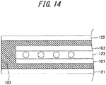
- a pouch structure such as illustrated in FIG. 14 may for example be adopted as a strategy for preventing infiltration of moisture at an edge.
- a phosphor layer 123 is sandwiched between a first film 101 and a second film 102, is further sandwiched between a first water vapor barrier film 121 and a second water vapor barrier film 122 disposed outward of the first film 101 and the second film 102, and is sealed by a sealing resin 103.
- the pouch structure has a large number of layers and cannot be easily manufactured.
- a tape sealing structure such as illustrated in FIG. 15 may be adopted.
- a phosphor layer 123 is sandwiched between a first water vapor barrier film 121 and a second water vapor barrier film 122, and edges of the first water vapor barrier film 121 and the second water vapor barrier film 122 are sealed by a sealing tape 130.
- the sealing tape structure has a small number of layers and can be easily manufactured. Examples of materials that can be used as this tape include aluminum foil, which is a good option for use as this tape, and other materials having water vapor permeability of no greater than 1 g/m 2 /day (40°C and 90% RH) such as PET (polyethylene terephthalate) vapor deposited on silica.
- the present disclosure provides a sealing tape that can prevent tape width misalignment, air bubble inclusion, and creasing even when the sealing tape is affixed in a folded state, and also provides a phosphor sheet in which this sealing tape is used, a lighting device, a liquid-crystal display, a method for manufacturing a phosphor sheet, and a sealing method.
- a sealing tape according to the present disclosure includes an adhesive layer, a gas barrier layer, a bonding layer, and a support film layer laminated in stated order, and has an incision into the support film layer in a thickness direction.
- the incision is located substantially centrally in a width direction and extends in a longitudinal direction.
- a phosphor sheet according to the present disclosure includes a first water vapor barrier film, a second water vapor barrier film, a phosphor layer sandwiched between the first water vapor barrier film and the second water vapor barrier film, and a sealing tape sealing edges of the first water vapor barrier film and the second water vapor barrier film.
- the sealing tape includes an adhesive layer, a gas barrier layer, a bonding layer, and a support film layer laminated in stated order, and has an incision into the support film layer in a thickness direction. The incision is located substantially centrally in a width direction and extends in a longitudinal direction.
- a lighting device includes the phosphor sheet described above.
- a liquid-crystal display according to the present disclosure includes the phosphor sheet described above.
- a method for producing a phosphor sheet according to the present disclosure includes sandwiching a phosphor layer between a first water vapor barrier film and a second water vapor barrier film, and affixing a sealing tape to edges of the first water vapor barrier film and the second water vapor barrier film.
- the sealing tape includes an adhesive layer, a gas barrier layer, a bonding layer, and a support film layer laminated in stated order, and has an incision into the support film layer in a thickness direction. The incision is located substantially centrally in a width direction and extends in a longitudinal direction.
- a sealing method includes affixing a sealing tape to edges of a first film and a second film.
- the sealing tape includes an adhesive layer, a gas barrier layer, a bonding layer, and a support film layer laminated in stated order, and has an incision into the support film layer in a thickness direction.
- the incision is located substantially centrally in a width direction and extends in a longitudinal direction.
- tape width misalignment, air bubble inclusion, and creasing can be prevented, even when the sealing tape is affixed in a folded state, as a result of the sealing tape having the incision into the support film layer in the thickness direction that is located substantially centrally in the width direction and extends in the longitudinal direction.
- FIG. 1 is a cross-sectional view illustrating configuration of a sealing tape according to a present embodiment.
- the sealing tape 10 includes an adhesive layer 11, a gas barrier layer 12, a bonding layer 13, and a support film layer 14 laminated in stated order, and has an incision 15 into the support film layer 14 in a thickness direction.
- the incision 15 is located substantially centrally in a width direction and extends in a longitudinal direction.
- the incision 15 located substantially centrally in the width direction and extending in the longitudinal direction may pass entirely through the support film layer 14 in the thickness direction. Furthermore, the incision 15 located substantially centrally in the width direction and extending in the longitudinal direction may pass partway through the bonding layer 13 in the thickness direction. Accordingly, the support film layer 14 can be easily folded at a fixed position and sealing workability can be improved.
- the adhesive layer 11 is a layer that is affixed to an adherend.
- An adhesive or bonding agent forming the adhesive layer 11 can be selected as appropriate depending on the material of the adherend.
- the adhesive layer 11 can be formed using an adhesive mainly containing an acrylic resin, an acrylic-modified silicone resin compound, a silicone-modified acrylic resin compound, or the like.
- the gas barrier layer 12 is a layer that has strong gas barrier properties with respect to at least water vapor and oxygen and is for example a substrate having water vapor permeability of no greater than 1 g/m 2 /day (40°C and 90% RH).
- the gas barrier layer 12 may for example be a single aluminum layer, the gas barrier layer 12 preferably includes an aluminum layer, a bonding layer, a substrate, a bonding layer, and an aluminum layer laminated in stated order. Curling may occur in situation in which an aluminum layer and a support film have a large extension and contraction ratio. However, curling can be restricted and sealing workability can be improved through symmetrical lamination of aluminum layers.
- a metal oxide such as silica or alumina may be used instead of aluminum such that the gas barrier layer 12 includes a metal oxide layer, a bonding layer, a substrate, a bonding layer, and a metal oxide layer laminated in stated order.
- the bonding layer 13 is for example composed of an ultraviolet curable resin or a thermoplastic resin.
- the bonding layer 13 has good transparency and is sufficiently adhesive with respect to the gas barrier layer 12 and the support film layer 14.
- No specific limitations are place on the ultraviolet curable resin or the thermoplastic resin, which can be a commonly known material.
- ultraviolet curable resins that can be used include acrylic resins and epoxy resins that are polymerized by photocuring agents.
- thermoplastic resins examples include acrylic resins, PS resins (polystyrene resins), AS resins (styrene-acrylonitrile copolymer resins), MS resins (styrene-methyl methacrylate copolymer resins), and SBC resins (styrene-butadiene block copolymer resins).
- acrylic resins PS resins (polystyrene resins), AS resins (styrene-acrylonitrile copolymer resins), MS resins (styrene-methyl methacrylate copolymer resins), and SBC resins (styrene-butadiene block copolymer resins).
- PS resins polystyrene resins
- AS resins styrene-acrylonitrile copolymer resins
- MS resins styrene-methyl methacrylate copolymer resins
- SBC resins styrene-butadiene block cop
- the bonding layer 13 preferably contains a phosphor.
- the phosphor is preferably a YAG phosphor or a nitride phosphor that is strongly resistant to moisture.
- a yellow YAG phosphor such as (Y,Gd) 3 (Al,Ga) 5 O 12 :Ce (YAG:Ce) is preferable in a situation in which white light is to be obtained using a blue LED.
- the thickness of the bonding layer 13 is preferably at least 10 ⁇ m and no greater than 50 ⁇ m in order to prevent an incision from being made as far as the gas barrier layer 12.
- the support film layer 14 is composed of a transparent plastic film that has a certain degree of stiffness.
- Specific examples that may be selected as appropriate depending on the intended use include non-stretched and stretched films of polyesters (for example, polyethylene terephthalate, polyethylene naphthalate, and polybutylene terephthalate), polyolefins (polyethylene, polypropylene), polyarylates, polycarbonates, polyacrylates, polyethersulfones, and copolymers of any of the preceding examples.
- the thickness of the support film layer 14 is preferably at least 10 ⁇ m and no greater than 50 ⁇ m.
- the sealing tape 10 configured as described above, a problem of tape width misalignment at the edge of an adherend when the sealing tape 10 is affixed in a folded state can be resolved because the folding position of the sealing tape 10 is fixed. Moreover, hardness of the support film layer 14 at the outermost surface can prevent air bubble inclusion and can restrict creasing caused by bending of the adherend. Furthermore, the gas barrier layer 12 can be protected from mechanical damage because the support film layer 14 is present at the outermost surface.
- FIG. 2 is a cross-sectional view illustrating an example of configuration at an edge of a phosphor sheet.
- the phosphor sheet includes a first water vapor barrier film 21, a second water vapor barrier film 22, a phosphor layer 23 sandwiched between the first water vapor barrier film 21 and the second water vapor barrier film 22, and the previously described sealing tape 10 sealing edges of the first water vapor barrier film 21 and the second water vapor barrier film 22.
- the width of the sealing tape 10 affixed onto the first water vapor barrier film 21 or the second water vapor barrier film 22 is preferably from 1 mm to 10 mm, and more preferably from 4 mm to 8 mm.
- the first water vapor barrier film 21 and the second water vapor barrier film 22 are for example each a substrate having water vapor permeability of no greater than 1 g/m 2 /day.
- the first water vapor barrier film 21 and the second water vapor barrier film 22 may each be a film having gas barrier properties in which a thin film of a metal oxide such as aluminum oxide, magnesium oxide, or silicon oxide is disposed on the surface of a film or a base plate made from a plastic such as PET (polyethylene terephthalate).
- the first water vapor barrier film 21 and the second water vapor barrier film 22 may each have a multilayer structure such as a PET/SiO x /PET structure.
- the phosphor layer 23 is a film formed from a resin composition containing the phosphor 23a in a powder state.
- the phosphor may for example be one or a combination of two or more of a sulfide phosphor, an oxide phosphor, a nitride phosphor, a fluoride phosphor, or the like depending on the phosphor type, the absorption region, the emission region, and so forth.
- sulfide phosphors that can be used include CaS:Eu, SrS:Eu, SrGa 2 S 4 :Eu, CaGa 2 S 4 :Eu, (Sr,Ca,Ba,Mg)Ga 2 S 4 :Eu, (Sr,Ca,Ba)S:Eu, Y 2 O 2 S:Eu, La 2 O 2 S:Eu, and Gd 2 O 2 S:Eu.
- oxide phosphors that can be used include (Ba,Sr) 3 SiO 5 :Eu, (Ba,Sr) 2 SiO 4 :Eu, Tb 3 Al 5 O 12 :Ce, and Ca 3 Sc 2 Si 3 O 12 :Ce.
- nitride phosphors that can be used include Ca 2 Si 5 N 8 :Eu, Sr 2 Si 5 N 8 :Eu, Ba 2 Si 5 N 8 :Eu, (Ca,Sr,Ba) 2 Si 5 N 8 :Eu, Ca x (Al,Si) 12 (O,N) 16 :Eu (0 ⁇ x ⁇ 1.5), CaSi 2 O 2 N 2 :Eu, SrSi 2 O 2 N 2 :Eu, BaSi 2 O 2 N 2 :Eu, (Ca,Sr,Ba)Si 2 O 2 N 2 :Eu, CaAl 2 Si 4 N 8 :Eu, CaSiN 2 :Eu, and CaAlSiN 3 :Eu.
- fluoride phosphors that can be used include K 2 TiF 6 :Mn 4+ , Ba 2 TiF 6 :Mn 4+ , Na 2 TiF 6 :Mn 4+ , K 3 ZrF 7 :Mn 4+ , and K 2 SiF 6 :Mn 4+ .
- fluoride phosphors examples include K 2 TiF 6 :Mn 4+ , Ba 2 TiF 6 :Mn 4+ , Na 2 TiF 6 :Mn 4+ , K 3 ZrF 7 :Mn 4+ , and K 2 SiF 6 :Mn 4+ .
- YAG phosphors such as (Y,Gd) 3 (Al,Ga) 5 O 12 :Ce (YAG:Ce)
- SiAlON phosphors such as Lu(Si,Al) 12 (O,N) 16 :Eu. Note that in the denotation of these phosphor materials, the part before the colon indicates the host material and the part
- Examples of phosphors that can be combined in order to obtain white light using a blue LED or a near ultraviolet LED include a yellow phosphor, a yellow phosphor with a red phosphor, and a green phosphor with a red phosphor.
- sulfide phosphors, oxide phosphors, and mixed phosphors thereof that are susceptible to degradation by water vapor can be favorably used and a wide color gamut can be reproduced.
- Examples of sulfide phosphors that can be combined in order to obtain white light using a blue LED include sulfide phosphors that exhibit a red fluorescence peak at a wavelength of from 620 nm to 660 nm upon irradiation with blue excitation light, with CaS:Eu and SrS:Eu being preferable, and sulfide phosphors that exhibit a green fluorescence peak at a wavelength of from 530 nm to 550 nm upon irradiation with blue excitation light, with SrGa 2 S 4 :Eu being preferable.
- the surface of a sulfide phosphor or an oxide phosphor is preferably coated.
- examples of compounds that can be used for this surface coating include oxides such as silicon oxide, yttrium oxide, aluminum oxide, and lanthanum oxide. Any one of these examples or a combination of any two or more of these examples may be used.
- a mixed phosphor including: a sulfide phosphor that emits red fluorescence of a wavelength of from 620 nm to 660 nm upon irradiation with blue excitation light or an oxide phosphor that emits red fluorescence of a wavelength of from 590 nm to 620 nm upon irradiation with blue excitation light; and a sulfide phosphor that emits green fluorescence of a wavelength of from 530 nm to 550 nm upon irradiation with blue excitation light.
- a particularly preferable combination is a mixed phosphor including: CaS:Eu or (BaSr) 3 SiO 5 :Eu that emits red fluorescence; and SrGa 2 S
- the resin composition forming the phosphor layer preferably includes either or both of a polyolefin copolymer component and a photocurable (meth)acrylic resin component.
- polystyrene copolymers examples include styrene copolymers and hydrogenated products thereof.
- styrene copolymers and hydrogenated products thereof that can be used include styrene-ethylene-butylene-styrene block copolymers and hydrogenated products thereof, and styrene-ethylene-propylene block copolymers and hydrogenated products thereof.
- a hydrogenated product of a styrene-ethylene-butylene-styrene block copolymer is particularly preferable in terms of transparency and gas barrier properties. Excellent light stability and low water absorbency can be obtained as a result of inclusion of a polyolefin copolymer component such as described above.
- Examples of the photocurable acrylate resin component include urethane (meth)acrylates, polyester (meth)acrylates, and epoxy (meth)acrylates.
- a urethane (meth)acrylate is preferable from a viewpoint of heat stability after photocuring. Excellent light stability and low water absorbency can be obtained as a result of inclusion of a photocurable (meth)acrylate resin component such as described above.
- the resin composition may include another light-transmitting resin, a color pigment, a solvent, or the like, as required, to the extent that the effects of the present disclosure are not lost.
- a method for manufacturing a phosphor sheet according to a present embodiment includes sandwiching a phosphor layer between a first water vapor barrier film and a second water vapor barrier film, and sealing edges of the first water vapor barrier film and the second water vapor barrier film using the previously described sealing tape.
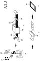
- FIG. 3 is a schematic diagram illustrating an example of the method for manufacturing the phosphor sheet.
- the method for manufacturing the phosphor sheet illustrated in FIG. 3 which is provided as a specific example, includes a stirring step (A), a lamination step (B), a punching step (C), and a sealing step (D).
- a phosphor-containing resin paste is obtained by, for example, mixing a predetermined blending ratio of a red phosphor 31 and a green phosphor 32 into a resin paste that has been dissolved using a solvent.
- a phosphor layer 23 is formed by applying the phosphor-containing resin paste onto a first water vapor barrier film 21, adjusting the phosphor-containing resin paste to a uniform film thickness using a bar coater 33, and drying the phosphor-containing resin paste in an oven 34.
- a second water vapor barrier film 22 is affixed onto the phosphor layer 23 using a thermal laminator 35 in order to obtain a phosphor sheet web in which the phosphor layer 23 is sandwiched between the first and second water vapor barrier films 21 and 22.
- the punching step (C) the phosphor sheet web is punched using a pressing machine 36 to obtain a phosphor sheet of a specific size having a side surface at the edge thereof at which the phosphor layer is exposed.
- the sealing step (D) the phosphor layer 23 is sealed by affixing the previously described sealing tape 10 to an edge of the first water vapor barrier film 21 and an edge of the second water vapor barrier film 22.
- a phosphor sheet can be obtained in which the sealing tape 10 is affixed to the edges of the first and second water vapor barrier films 21 and 22.
- the previously described sealing tape is not limited to use in a method for manufacturing a phosphor sheet and can also be used in a sealing method in which the sealing tape is affixed to edges of a first film and a second film.
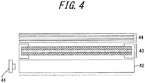
- FIG. 4 is a schematic cross-sectional view illustrating an edge-type lighting device.
- the lighting device is what may be referred to as an "edge-type backlight" and includes blue LEDs 41, a light guide plate 42 that emits light uniformly from a surface thereof through diffusion of blue light from the blue LEDs 41 that is incident on a side surface thereof, a phosphor sheet 43 used to obtain white light from the blue light, and an optical film group 44.
- the blue LEDs 41 form what may be referred to as an "LED package” that for example includes InGaN LED chips as blue light-emitting elements.
- the light guide plate 42 is for example a transparent substrate, such as an acrylic plate, that uniformly emits light that is incident on a side surface thereof by surface light emission.
- the phosphor sheet 43 contains a powder-state phosphor used to obtain white light from blue light emitted by the blue light-emitting elements.
- the powder of the phosphor has an average particle diameter on the scale of micrometers to tens of micrometers. Accordingly, light scattering effectiveness of the phosphor sheet 43 can be improved.
- the optical film group 44 for example includes a diffusion film and a reflective polarizing film for improving visibility of a liquid-crystal display.
- FIG. 5 is a schematic cross-sectional view illustrating a direct-type lighting device.
- the lighting device is what may be referred to as a "direct-type backlight" and includes a substrate 52 having a two-dimensional array of blue LEDs 51, a diffusion plate 53 that causes diffusion of blue light emitted from the blue LEDs 51, a phosphor sheet 43 that is separated from the substrate 52 and through which white light is obtained from the blue light, and an optical film group 44.
- the blue LEDs 51 form what may be referred to as an "LED package" that for example includes InGaN LED chips as blue light-emitting elements.
- the substrate 52 is made from a glass cloth substrate material in which a resin such as a phenolic resin, an epoxy resin, or a polyimide resin is used.
- the blue LEDs 51 are arranged at equal intervals with a specific pitch on the substrate 52 such as to be in a two-dimensional array that corresponds to the entire surface of the phosphor sheet 43. Note that a surface of the substrate 52 on which the blue LEDs 51 are mounted may be subjected to reflection treatment as required.
- the substrate 52 and the phosphor sheet 43 are separated by approximately 10 mm to 50 mm such that the lighting device has what may be referred to as a "remote phosphor structure.”
- a gap between the substrate 52 and the phosphor sheet 43 is maintained by a plurality of support columns or a reflector plate, and the support columns or reflector plate are disposed such as to surround a space formed by the substrate 52 and the phosphor sheet 43 on four sides.
- the diffusion plate 53 causes light emitted from the blue LEDs 51 to diffuse over a wide range to an extent that the shape of the light source is not visible.
- the diffusion plate 53 has a total light transmissivity of, for example, at least 20% and no greater than 80%.
- the edge of the phosphor sheet 43 is sealed by a cover member in order to allow favorable used of sulfide phosphors, oxide phosphors, and mixed phosphors thereof that are susceptible to degradation by water vapor.
- FIG. 6 illustrates spectra for a backlight in which sulfide phosphors were used and a backlight in which a conventional yellow phosphor was used.
- "a" indicates the spectrum of the backlight in which the sulfide phosphors were used and "b” indicates the spectrum of the backlight in which the conventional yellow phosphor was used.
- FIG. 7 is a CIE 1931 chromaticity diagram illustrating color spaces for a liquid-crystal display including the backlight in which the sulfide phosphors were used and a liquid-crystal display including the backlight in which the conventional yellow phosphor was used.
- "a" indicates the color space of the liquid-crystal display including the backlight in which the sulfide phosphors were used
- "b” indicates the color space of the liquid-crystal display including the backlight in which the conventional yellow phosphor was used
- “c” indicates an NTSC scheme color space
- “d” indicates an sRGB scheme color space.
- a green sulfide phosphor (SrGa 2 S 4 :Eu) and a red sulfide phosphor (CaS:Eu) were used as the sulfide phosphors, and a phosphor sheet was used in which the sulfide phosphors were dispersed in a styrene-ethylene-butylene-styrene block (SEBS) resin.
- SEBS styrene-ethylene-butylene-styrene block
- the spectrum "a" of the backlight in which the sulfide phosphors were used had a greater intensity near 650 nm than the spectrum "b" of the backlight in which the yellow phosphor was used as a consequence of the phosphor sheet in which the sulfide phosphors were used containing the red sulfide phosphor.
- the spectrum "a" of the backlight in which the sulfide phosphors were used had a greater intensity near 650 nm than the spectrum "b" of the backlight in which the yellow phosphor was used as a consequence of the phosphor sheet in which the sulfide phosphors were used containing the red sulfide phosphor.
- the color space of the liquid-crystal display including the backlight in which the sulfide phosphors were used had an area ratio of approximately 85% to 90% relative to the NTSC scheme color space
- the color space of the liquid-crystal display including the backlight in which the yellow phosphor was used had an area ratio of approximately 72% relative to the NTSC scheme color space.
- the area ratio is determined by the product of the backlight spectrum and the spectral transmittance of a color filter inside the liquid-crystal display. It will be appreciated that the value of the area ratio may be somewhat larger or smaller depending on the spectral transmittance of the color filter.
- phosphor sheets in which sulfide phosphors are used can express a wide color gamut. Therefore, a technique such as described in the present embodiment for sealing the edge of a phosphor sheet with a cover member in order to prevent infiltration of water vapor is extremely useful for phosphor sheets in which sulfide phosphors are used. Furthermore, by providing a lighting device including a phosphor sheet in which a sulfide phosphor is used in, for example, a liquid-crystal panel forming a display screen of a liquid-crystal display, not only can a wide color gamut be expressed, but also the life of the liquid-crystal display can be extended.
- the lighting device may alternatively be used as a light source for lighting.
- the optical films 34 can normally be omitted.
- the phosphor-containing resin may have a three-dimensional shape such as a cup-like shape instead of having a flat sheet shape.
- sealing tapes having different configurations were prepared. Evaluation of tape width misalignment, air bubble inclusion, and creasing was performed for when each of the sealing tapes was affixed to the edge of a phosphor sheet and was folded to seal the edge.
- the present disclosure is in no way limited to these examples.
- the phosphor sheet included a phosphor layer of approximately 40 ⁇ m in thickness sandwiched between water vapor barrier films and had a 65-inch size (1450 mm x 820 mm). The thickness of the phosphor sheet was approximately 130 ⁇ m.
- a sealing tape of approximately 6 mm in width was used to seal the edge of a phosphor sheet.
- the tape width at the edge of the phosphor sheet was measured and front/rear tape width misalignment was evaluated. An evaluation of "good” was given when the tape width was within 3 ⁇ 0.5 mm and an evaluation of "poor” was given when the tape width was not within 3 ⁇ 0.5 mm.
- a sealing tape of approximately 6 mm in width was used to seal the edge of a phosphor sheet. The sealing tape was observed and an evaluation of "good” was given when included air bubbles were less than 1 mm 2 , whereas an evaluation of "poor” was given when included air bubbles were 1 mm 2 or greater.
- a sealing tape of approximately 6 mm in width was used to seal the edge of a phosphor sheet.
- the sealing tape was observed after folding the phosphor sheet and an evaluation of "good” was given when creasing did not occur, whereas an evaluation of "poor” was given when creasing occurred.
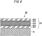
- FIG. 8 is a schematic cross-sectional view illustrating tape structure in Comparative Example 1.
- a sealing tape 60 in Comparative Example 1 included an adhesive layer 61 and a gas barrier layer 62.
- the adhesive layer 61 was an acrylic adhesive layer of approximately 25 ⁇ m in thickness.
- the gas barrier layer 61 included an aluminum layer 621 of approximately 7 ⁇ m in thickness, a bonding layer 622 of approximately 3 ⁇ m in thickness, a PET film 623 of approximately 12 ⁇ m in thickness, a bonding layer 624 of approximately 3 ⁇ m in thickness, and an aluminum layer 625 of approximately 7 ⁇ m in thickness laminated in stated order.
- Comparative Example 1 The tape structure in Comparative Example 1 was subjected to slitting to a width of approximately 6 mm to obtain a sealing tape of Comparative Example 1.
- the sealing tape of Comparative Example 1 was used to seal the edge of a phosphor sheet.
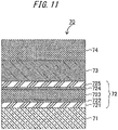
- FIG. 11 is a schematic cross-sectional view illustrating tape structure in Comparative Example 2.
- a sealing tape 70 in Comparative Example 2 included an adhesive layer 71, a gas barrier layer 72, a bonding layer 73, and a support film layer 74.
- the adhesive layer 71 was an acrylic adhesive layer of approximately 25 ⁇ m in thickness.
- the gas barrier layer 72 included an aluminum layer 721 of approximately 7 ⁇ m in thickness, a bonding layer 722 of approximately 3 ⁇ m in thickness, a PET film 723 of approximately 12 ⁇ m in thickness, a bonding layer 724 of approximately 3 ⁇ m in thickness, and an aluminum layer 725 of approximately 7 ⁇ m in thickness laminated in stated order.
- the bonding layer 73 was a thermoplastic resin layer of approximately 25 ⁇ m in thickness.
- the support film layer 74 was a PET film of approximately 25 ⁇ m in thickness.
- Comparative Example 2 The tape structure in Comparative Example 2 was subjected to slitting to a width of approximately 6 mm to obtain a sealing tape of Comparative Example 2.
- the sealing tape of Comparative Example 2 was used to seal the edge of a phosphor sheet.
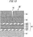
- FIG. 13 is a schematic cross-sectional view illustrating tape structure in Example 1.
- a sealing tape 80 in Example 1 included an adhesive layer 81, a gas barrier layer 82, a bonding layer 83, and a support film layer 84.
- the adhesive layer 81 was an acrylic adhesive layer of approximately 25 ⁇ m in thickness.
- the gas barrier layer 81 included an aluminum layer 821 of approximately 7 ⁇ m in thickness, a bonding layer 822 of approximately 3 ⁇ m in thickness, a PET film 823 of approximately 12 ⁇ m in thickness, a bonding layer 824 of approximately 3 ⁇ m in thickness, and an aluminum layer 825 of approximately 7 ⁇ m in thickness laminated in stated order.
- the bonding layer 83 was a thermoplastic resin layer of approximately 25 ⁇ m in thickness.
- the support film layer 84 was a PET film of approximately 25 ⁇ m in thickness.
- Example 1 The tape structure in Example 1 was subjected to slitting to a width of approximately 6 mm and a half cut was subsequently made centrally in the sealing tape. Specifically, an incision was made through the 25- ⁇ m PET film at the outermost surface and partway through the bonding layer. The resultant sealing tape was used as a sealing tape of Example 1 in order to seal the edge of a phosphor sheet.
- Example 1 tape width misalignment, air bubble inclusion, and creasing were each evaluated as good in Example 1.
- a folding position could be clearly determined as a result of the incision being provided into the PET film forming the support film layer 84, and thus no significant misalignment of tape width at the front and rear occurred.
- inclusion of air bubbles did not occur due to the hardness of the PET film forming the support film layer 84.
- creasing did not occur in the tape part even when the phosphor sheet was folded.
Landscapes
- Physics & Mathematics (AREA)
- Nonlinear Science (AREA)
- Optics & Photonics (AREA)
- Chemical & Material Sciences (AREA)
- General Physics & Mathematics (AREA)
- Mathematical Physics (AREA)
- Crystallography & Structural Chemistry (AREA)
- Engineering & Computer Science (AREA)
- General Engineering & Computer Science (AREA)
- Microelectronics & Electronic Packaging (AREA)
- Organic Chemistry (AREA)
- Liquid Crystal (AREA)
- Adhesive Tapes (AREA)
- Laminated Bodies (AREA)
- Luminescent Compositions (AREA)
- Planar Illumination Modules (AREA)
- Spectroscopy & Molecular Physics (AREA)
- Adhesives Or Adhesive Processes (AREA)
- Non-Portable Lighting Devices Or Systems Thereof (AREA)
- Sealing Material Composition (AREA)
- Led Device Packages (AREA)
Abstract
Description
- The present application claims priority of Japanese Patent Application No.
2014-32279 (filed on February 21, 2014 - The present disclosure relates to a sealing tape that blocks water vapor, a phosphor sheet in which the sealing tape is used, a lighting device, a liquid-crystal display, a method for manufacturing a phosphor sheet, and a sealing method.
- A backlight-type light source is used in a liquid-crystal display in order to irradiate a liquid-crystal panel from the back to a front surface thereof. In recent years, in accompaniment to trends toward larger, thinner, lighter, and longer life liquid-crystal displays, and from a viewpoint of improving video properties of such liquid-crystal displays through on/off control, there has been much interest in light-emitting devices that perform surface light emission through an array of light-emitting diodes (LEDs) mounted on a substrate. Extraction of white light from such light-emitting devices is mainly carried out by the following two methods.
- The first of these methods involves providing LEDs that emit light of three colors, R, G, and B, and turning on these LEDs simultaneously such that white light is obtained as a composite of light of these three colors. The second of these methods involves, for example, encapsulating a blue LED in a phosphor-containing resin such that white light is obtained through color conversion of blue light. The structure composed by encapsulation of the blue LED in the phosphor-containing resin is referred to as a "white LED."
- However, the first method is expensive because LEDs of three colors, R, G, and B, are required. On the other hand, potting with the phosphor-containing resin in the second method is carried out against an extremely small LED surface area, which makes it difficult to uniformly form the phosphor-containing resin without unevenness.
- For this reason, in recent years there has been interest in a third method that can be used in place of the second method and that involves performing color conversion with respect to blue LEDs using a structure in which a phosphor-containing resin is sandwiched between sheet substrates or a phosphor-containing sheet formed by processing a phosphor-containing resin into a sheet shape (for example, refer to PTL 1 and 2).
- Phosphors are vulnerable to oxygen and water vapor. For example, although sulfide phosphors such as SrGa2S4:Eu, CaS:Eu, and SrS:Eu are excellent phosphor materials that can be used to reproduce a wide color gamut due to their sharp emission spectra and (Ba,Sr)3SiO5:Eu can be used as an orange light-emitting phosphor material having high brightness, degradation of these phosphors due to water vapor readily occurs in a high temperature and high humidity environment.
- Therefore, it is necessary to provide a means for blocking water vapor when using these phosphors. Although it is difficult to adopt these phosphors in white LEDs, in the case of the aforementioned third method, the problem described above can be dealt with by, for example, covering a phosphor layer with a water vapor barrier film. Examples of such methods that have been proposed include a method in which a protective layer of a silicon compound or the like is provided on a phosphor-containing resin (refer to PTL 3) and a method in which a water vapor barrier layer is formed on the surface of a phosphor-containing resin (refer to PTL 4 and 5).
- A pouch structure such as illustrated in
FIG. 14 may for example be adopted as a strategy for preventing infiltration of moisture at an edge. In the pouch structure, aphosphor layer 123 is sandwiched between afirst film 101 and asecond film 102, is further sandwiched between a first watervapor barrier film 121 and a second watervapor barrier film 122 disposed outward of thefirst film 101 and thesecond film 102, and is sealed by asealing resin 103. The pouch structure has a large number of layers and cannot be easily manufactured. - Alternatively, a tape sealing structure such as illustrated in
FIG. 15 may be adopted. In the tape sealing structure, aphosphor layer 123 is sandwiched between a first watervapor barrier film 121 and a second watervapor barrier film 122, and edges of the first watervapor barrier film 121 and the second watervapor barrier film 122 are sealed by asealing tape 130. The sealing tape structure has a small number of layers and can be easily manufactured. Examples of materials that can be used as this tape include aluminum foil, which is a good option for use as this tape, and other materials having water vapor permeability of no greater than 1 g/m2/day (40°C and 90% RH) such as PET (polyethylene terephthalate) vapor deposited on silica. -
- PTL 1:
JP 2005-108635 A - PTL 2:
JP 2009-283438 A - PTL 3:
JP H6-58440 B - PTL 4:
JP 2009-283441 A - PTL 5:
JP 2011-13567 A - However, when a conventional sealing tape is affixed in a folded state, tape width misalignment, air bubble inclusion, creasing, or the like may cause deficient edge sealing.
- In consideration of the situation described above, the present disclosure provides a sealing tape that can prevent tape width misalignment, air bubble inclusion, and creasing even when the sealing tape is affixed in a folded state, and also provides a phosphor sheet in which this sealing tape is used, a lighting device, a liquid-crystal display, a method for manufacturing a phosphor sheet, and a sealing method.
- In order to solve the problem described above, a sealing tape according to the present disclosure includes an adhesive layer, a gas barrier layer, a bonding layer, and a support film layer laminated in stated order, and has an incision into the support film layer in a thickness direction. The incision is located substantially centrally in a width direction and extends in a longitudinal direction.
- A phosphor sheet according to the present disclosure includes a first water vapor barrier film, a second water vapor barrier film, a phosphor layer sandwiched between the first water vapor barrier film and the second water vapor barrier film, and a sealing tape sealing edges of the first water vapor barrier film and the second water vapor barrier film. The sealing tape includes an adhesive layer, a gas barrier layer, a bonding layer, and a support film layer laminated in stated order, and has an incision into the support film layer in a thickness direction. The incision is located substantially centrally in a width direction and extends in a longitudinal direction.
- A lighting device according to the present disclosure includes the phosphor sheet described above.
- A liquid-crystal display according to the present disclosure includes the phosphor sheet described above.
- A method for producing a phosphor sheet according to the present disclosure includes sandwiching a phosphor layer between a first water vapor barrier film and a second water vapor barrier film, and affixing a sealing tape to edges of the first water vapor barrier film and the second water vapor barrier film. The sealing tape includes an adhesive layer, a gas barrier layer, a bonding layer, and a support film layer laminated in stated order, and has an incision into the support film layer in a thickness direction. The incision is located substantially centrally in a width direction and extends in a longitudinal direction.
- A sealing method according to the present disclosure includes affixing a sealing tape to edges of a first film and a second film. The sealing tape includes an adhesive layer, a gas barrier layer, a bonding layer, and a support film layer laminated in stated order, and has an incision into the support film layer in a thickness direction. The incision is located substantially centrally in a width direction and extends in a longitudinal direction.
- According to the present disclosure, tape width misalignment, air bubble inclusion, and creasing can be prevented, even when the sealing tape is affixed in a folded state, as a result of the sealing tape having the incision into the support film layer in the thickness direction that is located substantially centrally in the width direction and extends in the longitudinal direction.
- In the accompanying drawings:
-
FIG. 1 is a cross-sectional view illustrating configuration of a sealing tape according to a present embodiment; -
FIG. 2 is a cross-sectional view illustrating an example of configuration at an edge of a phosphor sheet; -
FIG. 3 is a schematic diagram illustrating an example of a method for manufacturing a phosphor sheet; -
FIG. 4 is a schematic cross-sectional view illustrating an edge-type lighting device; -
FIG. 5 is a schematic cross-sectional view illustrating a direct-type lighting device; -
FIG. 6 illustrates spectra for a backlight in which sulfide phosphors were used and a backlight in which a conventional yellow phosphor was used; -
FIG. 7 is a CIE 1931 chromaticity diagram illustrating color spaces for a liquid-crystal display including the backlight in which the sulfide phosphors were used and a liquid-crystal display including the backlight in which the conventional yellow phosphor was used; -
FIG. 8 is a schematic cross-sectional view illustrating tape structure in Comparative Example 1; -
FIG. 9 is a schematic cross-sectional view illustrating tape width misalignment; -
FIG. 10 is a schematic cross-sectional view illustrating air bubble inclusion; -
FIG. 11 is a schematic cross-sectional view illustrating tape structure in Comparative Example 2; -
FIG. 12 is a schematic cross-sectional view illustrating a state in which folding is not possible; -
FIG. 13 is a schematic cross-sectional view illustrating tape structure in Example 1; -
FIG. 14 is a cross-sectional view illustrating a pouch structure of a conventional phosphor sheet; and -
FIG. 15 is a cross-sectional view illustrating a tape sealing structure of a conventional phosphor sheet. - A detailed description of embodiments of the present disclosure is provided in the following order with reference to the drawings.
- 1. Sealing tape
- 2. Phosphor sheet
- 3. Lighting device
- 4. Examples
-
FIG. 1 is a cross-sectional view illustrating configuration of a sealing tape according to a present embodiment. The sealingtape 10 includes anadhesive layer 11, agas barrier layer 12, abonding layer 13, and asupport film layer 14 laminated in stated order, and has anincision 15 into thesupport film layer 14 in a thickness direction. Theincision 15 is located substantially centrally in a width direction and extends in a longitudinal direction. As a result, thesupport film layer 14 can be folded at a fixed position and upward/downward width misalignment, air bubble inclusion, and creasing can be prevented even when the sealingtape 10 is affixed in a folded state. - Note that the
incision 15 located substantially centrally in the width direction and extending in the longitudinal direction may pass entirely through thesupport film layer 14 in the thickness direction. Furthermore, theincision 15 located substantially centrally in the width direction and extending in the longitudinal direction may pass partway through thebonding layer 13 in the thickness direction. Accordingly, thesupport film layer 14 can be easily folded at a fixed position and sealing workability can be improved. - The
adhesive layer 11 is a layer that is affixed to an adherend. An adhesive or bonding agent forming theadhesive layer 11 can be selected as appropriate depending on the material of the adherend. For example, theadhesive layer 11 can be formed using an adhesive mainly containing an acrylic resin, an acrylic-modified silicone resin compound, a silicone-modified acrylic resin compound, or the like. - The
gas barrier layer 12 is a layer that has strong gas barrier properties with respect to at least water vapor and oxygen and is for example a substrate having water vapor permeability of no greater than 1 g/m2/day (40°C and 90% RH). Although thegas barrier layer 12 may for example be a single aluminum layer, thegas barrier layer 12 preferably includes an aluminum layer, a bonding layer, a substrate, a bonding layer, and an aluminum layer laminated in stated order. Curling may occur in situation in which an aluminum layer and a support film have a large extension and contraction ratio. However, curling can be restricted and sealing workability can be improved through symmetrical lamination of aluminum layers. - A metal oxide such as silica or alumina may be used instead of aluminum such that the
gas barrier layer 12 includes a metal oxide layer, a bonding layer, a substrate, a bonding layer, and a metal oxide layer laminated in stated order. - The
bonding layer 13 is for example composed of an ultraviolet curable resin or a thermoplastic resin. Thebonding layer 13 has good transparency and is sufficiently adhesive with respect to thegas barrier layer 12 and thesupport film layer 14. No specific limitations are place on the ultraviolet curable resin or the thermoplastic resin, which can be a commonly known material. Examples of ultraviolet curable resins that can be used include acrylic resins and epoxy resins that are polymerized by photocuring agents. Examples of thermoplastic resins that can be used include acrylic resins, PS resins (polystyrene resins), AS resins (styrene-acrylonitrile copolymer resins), MS resins (styrene-methyl methacrylate copolymer resins), and SBC resins (styrene-butadiene block copolymer resins). Among these examples, a thermoplastic acrylic resin having excellent transparency is preferably used. - The
bonding layer 13 preferably contains a phosphor. Although no specific limitations are placed on the phosphor, the phosphor is preferably a YAG phosphor or a nitride phosphor that is strongly resistant to moisture. In particular, a yellow YAG phosphor such as (Y,Gd)3(Al,Ga)5O12:Ce (YAG:Ce) is preferable in a situation in which white light is to be obtained using a blue LED. By using the sealing tape at the edge of a phosphor sheet, a problem of bluish appearance near the edge of the phosphor sheet can be resolved. - The thickness of the
bonding layer 13 is preferably at least 10 µm and no greater than 50 µm in order to prevent an incision from being made as far as thegas barrier layer 12. - The
support film layer 14 is composed of a transparent plastic film that has a certain degree of stiffness. Specific examples that may be selected as appropriate depending on the intended use include non-stretched and stretched films of polyesters (for example, polyethylene terephthalate, polyethylene naphthalate, and polybutylene terephthalate), polyolefins (polyethylene, polypropylene), polyarylates, polycarbonates, polyacrylates, polyethersulfones, and copolymers of any of the preceding examples. - If the
support film layer 14 is too thin, an appropriate degree of stiffness cannot be obtained, whereas if thesupport film layer 14 is too thick, the tape thickness increases. Accordingly, the thickness of thesupport film layer 14 is preferably at least 10 µm and no greater than 50 µm. - Through the sealing
tape 10 configured as described above, a problem of tape width misalignment at the edge of an adherend when the sealingtape 10 is affixed in a folded state can be resolved because the folding position of the sealingtape 10 is fixed. Moreover, hardness of thesupport film layer 14 at the outermost surface can prevent air bubble inclusion and can restrict creasing caused by bending of the adherend. Furthermore, thegas barrier layer 12 can be protected from mechanical damage because thesupport film layer 14 is present at the outermost surface. -
FIG. 2 is a cross-sectional view illustrating an example of configuration at an edge of a phosphor sheet. The phosphor sheet includes a first watervapor barrier film 21, a second watervapor barrier film 22, aphosphor layer 23 sandwiched between the first watervapor barrier film 21 and the second watervapor barrier film 22, and the previously described sealingtape 10 sealing edges of the first watervapor barrier film 21 and the second watervapor barrier film 22. - From a viewpoint of strength and water vapor barrier properties, the width of the sealing
tape 10 affixed onto the first watervapor barrier film 21 or the second watervapor barrier film 22 is preferably from 1 mm to 10 mm, and more preferably from 4 mm to 8 mm. - Through the phosphor sheet having the configuration described above, infiltration of water vapor into the
phosphor layer 23 at the edges of the water vapor barrier films can be prevented and thus degradation of aphosphor 23a in thephosphor layer 23 can be prevented. - The first water
vapor barrier film 21 and the second watervapor barrier film 22 are for example each a substrate having water vapor permeability of no greater than 1 g/m2/day. For example, the first watervapor barrier film 21 and the second watervapor barrier film 22 may each be a film having gas barrier properties in which a thin film of a metal oxide such as aluminum oxide, magnesium oxide, or silicon oxide is disposed on the surface of a film or a base plate made from a plastic such as PET (polyethylene terephthalate). Alternatively, the first watervapor barrier film 21 and the second watervapor barrier film 22 may each have a multilayer structure such as a PET/SiOx/PET structure. - The
phosphor layer 23 is a film formed from a resin composition containing thephosphor 23a in a powder state. Although no specific limitations are placed on the phosphor, the phosphor may for example be one or a combination of two or more of a sulfide phosphor, an oxide phosphor, a nitride phosphor, a fluoride phosphor, or the like depending on the phosphor type, the absorption region, the emission region, and so forth. - Specific examples of sulfide phosphors that can be used include CaS:Eu, SrS:Eu, SrGa2S4:Eu, CaGa2S4:Eu, (Sr,Ca,Ba,Mg)Ga2S4:Eu, (Sr,Ca,Ba)S:Eu, Y2O2S:Eu, La2O2S:Eu, and Gd2O2S:Eu. Specific examples of oxide phosphors that can be used include (Ba,Sr)3SiO5:Eu, (Ba,Sr)2SiO4:Eu, Tb3Al5O12:Ce, and Ca3Sc2Si3O12:Ce. Specific examples of nitride phosphors that can be used include Ca2Si5N8:Eu, Sr2Si5N8:Eu, Ba2Si5N8:Eu, (Ca,Sr,Ba)2Si5N8:Eu, Cax(Al,Si)12(O,N)16:Eu (0 < x ≤ 1.5), CaSi2O2N2:Eu, SrSi2O2N2:Eu, BaSi2O2N2:Eu, (Ca,Sr,Ba)Si2O2N2:Eu, CaAl2Si4N8:Eu, CaSiN2:Eu, and CaAlSiN3:Eu. Specific examples of fluoride phosphors that can be used include K2TiF6:Mn4+, Ba2TiF6:Mn4+, Na2TiF6:Mn4+, K3ZrF7:Mn4+, and K2SiF6:Mn4+. Examples of other phosphors that can be used include YAG phosphors such as (Y,Gd)3(Al,Ga)5O12:Ce (YAG:Ce) and SiAlON phosphors such as Lu(Si,Al)12(O,N)16:Eu. Note that in the denotation of these phosphor materials, the part before the colon indicates the host material and the part after the colon indicates the activator.
- Examples of phosphors that can be combined in order to obtain white light using a blue LED or a near ultraviolet LED include a yellow phosphor, a yellow phosphor with a red phosphor, and a green phosphor with a red phosphor. In the present embodiment, sulfide phosphors, oxide phosphors, and mixed phosphors thereof that are susceptible to degradation by water vapor can be favorably used and a wide color gamut can be reproduced.
- Examples of sulfide phosphors that can be combined in order to obtain white light using a blue LED include sulfide phosphors that exhibit a red fluorescence peak at a wavelength of from 620 nm to 660 nm upon irradiation with blue excitation light, with CaS:Eu and SrS:Eu being preferable, and sulfide phosphors that exhibit a green fluorescence peak at a wavelength of from 530 nm to 550 nm upon irradiation with blue excitation light, with SrGa2S4:Eu being preferable.
- Examples of oxide phosphors that can be combined in order to obtain white light using a blue LED include oxide phosphors that exhibit red fluorescence of a wavelength of from 590 nm to 620 nm upon irradiation with blue excitation light, with (Ba,Sr)3SiO5:Eu and (Ba,Sr)2SiO4:Eu being preferable.
- Note that besides the sulfide phosphors or oxide phosphors combined in order to obtain white light using a blue LED, other phosphors such as (Y,Gd)3(Al,Ga)5O12:Ce or a SiAlON phosphor may be used.
- The surface of a sulfide phosphor or an oxide phosphor is preferably coated. Examples of compounds that can be used for this surface coating include oxides such as silicon oxide, yttrium oxide, aluminum oxide, and lanthanum oxide. Any one of these examples or a combination of any two or more of these examples may be used.
- In a situation in which a mixture of phosphors such as described above is used as the phosphor in a single layer-type light-emitter sheet illustrated in
FIG. 2 , in order that the phosphor sheet emits white light, it is preferable to use a mixed phosphor including: a sulfide phosphor that emits red fluorescence of a wavelength of from 620 nm to 660 nm upon irradiation with blue excitation light or an oxide phosphor that emits red fluorescence of a wavelength of from 590 nm to 620 nm upon irradiation with blue excitation light; and a sulfide phosphor that emits green fluorescence of a wavelength of from 530 nm to 550 nm upon irradiation with blue excitation light. A particularly preferable combination is a mixed phosphor including: CaS:Eu or (BaSr)3SiO5:Eu that emits red fluorescence; and SrGa2S4:Eu that emits green fluorescence. - The resin composition forming the phosphor layer preferably includes either or both of a polyolefin copolymer component and a photocurable (meth)acrylic resin component.
- Examples of the polyolefin copolymer include styrene copolymers and hydrogenated products thereof. Preferable examples of styrene copolymers and hydrogenated products thereof that can be used include styrene-ethylene-butylene-styrene block copolymers and hydrogenated products thereof, and styrene-ethylene-propylene block copolymers and hydrogenated products thereof. Among these example, a hydrogenated product of a styrene-ethylene-butylene-styrene block copolymer is particularly preferable in terms of transparency and gas barrier properties. Excellent light stability and low water absorbency can be obtained as a result of inclusion of a polyolefin copolymer component such as described above.
- Examples of the photocurable acrylate resin component include urethane (meth)acrylates, polyester (meth)acrylates, and epoxy (meth)acrylates. Among these examples, a urethane (meth)acrylate is preferable from a viewpoint of heat stability after photocuring. Excellent light stability and low water absorbency can be obtained as a result of inclusion of a photocurable (meth)acrylate resin component such as described above.
- The resin composition may include another light-transmitting resin, a color pigment, a solvent, or the like, as required, to the extent that the effects of the present disclosure are not lost.
- A method for manufacturing a phosphor sheet according to a present embodiment includes sandwiching a phosphor layer between a first water vapor barrier film and a second water vapor barrier film, and sealing edges of the first water vapor barrier film and the second water vapor barrier film using the previously described sealing tape.
-
FIG. 3 is a schematic diagram illustrating an example of the method for manufacturing the phosphor sheet. The method for manufacturing the phosphor sheet illustrated inFIG. 3 , which is provided as a specific example, includes a stirring step (A), a lamination step (B), a punching step (C), and a sealing step (D). - In the stirring step (A), a phosphor-containing resin paste is obtained by, for example, mixing a predetermined blending ratio of a
red phosphor 31 and agreen phosphor 32 into a resin paste that has been dissolved using a solvent. In the lamination step (B), aphosphor layer 23 is formed by applying the phosphor-containing resin paste onto a first watervapor barrier film 21, adjusting the phosphor-containing resin paste to a uniform film thickness using abar coater 33, and drying the phosphor-containing resin paste in anoven 34. Thereafter, a second watervapor barrier film 22 is affixed onto thephosphor layer 23 using athermal laminator 35 in order to obtain a phosphor sheet web in which thephosphor layer 23 is sandwiched between the first and second watervapor barrier films pressing machine 36 to obtain a phosphor sheet of a specific size having a side surface at the edge thereof at which the phosphor layer is exposed. In the sealing step (D), thephosphor layer 23 is sealed by affixing the previously described sealingtape 10 to an edge of the first watervapor barrier film 21 and an edge of the second watervapor barrier film 22. - Through the steps (A) to (D) described above, a phosphor sheet can be obtained in which the sealing
tape 10 is affixed to the edges of the first and second watervapor barrier films - The previously described sealing tape is not limited to use in a method for manufacturing a phosphor sheet and can also be used in a sealing method in which the sealing tape is affixed to edges of a first film and a second film.
-
FIG. 4 is a schematic cross-sectional view illustrating an edge-type lighting device. As the illustrated inFIG. 4 , the lighting device is what may be referred to as an "edge-type backlight" and includesblue LEDs 41, alight guide plate 42 that emits light uniformly from a surface thereof through diffusion of blue light from theblue LEDs 41 that is incident on a side surface thereof, aphosphor sheet 43 used to obtain white light from the blue light, and anoptical film group 44. - The
blue LEDs 41 form what may be referred to as an "LED package" that for example includes InGaN LED chips as blue light-emitting elements. Thelight guide plate 42 is for example a transparent substrate, such as an acrylic plate, that uniformly emits light that is incident on a side surface thereof by surface light emission. Thephosphor sheet 43 contains a powder-state phosphor used to obtain white light from blue light emitted by the blue light-emitting elements. The powder of the phosphor has an average particle diameter on the scale of micrometers to tens of micrometers. Accordingly, light scattering effectiveness of thephosphor sheet 43 can be improved. Theoptical film group 44 for example includes a diffusion film and a reflective polarizing film for improving visibility of a liquid-crystal display. -
FIG. 5 is a schematic cross-sectional view illustrating a direct-type lighting device. As illustrated inFIG. 5 , the lighting device is what may be referred to as a "direct-type backlight" and includes asubstrate 52 having a two-dimensional array ofblue LEDs 51, adiffusion plate 53 that causes diffusion of blue light emitted from theblue LEDs 51, aphosphor sheet 43 that is separated from thesubstrate 52 and through which white light is obtained from the blue light, and anoptical film group 44. - The
blue LEDs 51 form what may be referred to as an "LED package" that for example includes InGaN LED chips as blue light-emitting elements. Thesubstrate 52 is made from a glass cloth substrate material in which a resin such as a phenolic resin, an epoxy resin, or a polyimide resin is used. Theblue LEDs 51 are arranged at equal intervals with a specific pitch on thesubstrate 52 such as to be in a two-dimensional array that corresponds to the entire surface of thephosphor sheet 43. Note that a surface of thesubstrate 52 on which theblue LEDs 51 are mounted may be subjected to reflection treatment as required. Thesubstrate 52 and thephosphor sheet 43 are separated by approximately 10 mm to 50 mm such that the lighting device has what may be referred to as a "remote phosphor structure." A gap between thesubstrate 52 and thephosphor sheet 43 is maintained by a plurality of support columns or a reflector plate, and the support columns or reflector plate are disposed such as to surround a space formed by thesubstrate 52 and thephosphor sheet 43 on four sides. Thediffusion plate 53 causes light emitted from theblue LEDs 51 to diffuse over a wide range to an extent that the shape of the light source is not visible. Thediffusion plate 53 has a total light transmissivity of, for example, at least 20% and no greater than 80%. - In the lighting device configured as described above, the edge of the
phosphor sheet 43 is sealed by a cover member in order to allow favorable used of sulfide phosphors, oxide phosphors, and mixed phosphors thereof that are susceptible to degradation by water vapor. -
FIG. 6 illustrates spectra for a backlight in which sulfide phosphors were used and a backlight in which a conventional yellow phosphor was used. InFIG. 6 , "a" indicates the spectrum of the backlight in which the sulfide phosphors were used and "b" indicates the spectrum of the backlight in which the conventional yellow phosphor was used. -
FIG. 7 is a CIE 1931 chromaticity diagram illustrating color spaces for a liquid-crystal display including the backlight in which the sulfide phosphors were used and a liquid-crystal display including the backlight in which the conventional yellow phosphor was used. InFIG. 7 , "a" indicates the color space of the liquid-crystal display including the backlight in which the sulfide phosphors were used, "b" indicates the color space of the liquid-crystal display including the backlight in which the conventional yellow phosphor was used, "c" indicates an NTSC scheme color space, and "d" indicates an sRGB scheme color space. - In the backlight in which the sulfide phosphors were used, a green sulfide phosphor (SrGa2S4:Eu) and a red sulfide phosphor (CaS:Eu) were used as the sulfide phosphors, and a phosphor sheet was used in which the sulfide phosphors were dispersed in a styrene-ethylene-butylene-styrene block (SEBS) resin.
- As illustrated in
FIG. 6 , the spectrum "a" of the backlight in which the sulfide phosphors were used had a greater intensity near 650 nm than the spectrum "b" of the backlight in which the yellow phosphor was used as a consequence of the phosphor sheet in which the sulfide phosphors were used containing the red sulfide phosphor. Moreover, as illustrated inFIG. 7 , the color space of the liquid-crystal display including the backlight in which the sulfide phosphors were used had an area ratio of approximately 85% to 90% relative to the NTSC scheme color space, whereas the color space of the liquid-crystal display including the backlight in which the yellow phosphor was used had an area ratio of approximately 72% relative to the NTSC scheme color space. The area ratio is determined by the product of the backlight spectrum and the spectral transmittance of a color filter inside the liquid-crystal display. It will be appreciated that the value of the area ratio may be somewhat larger or smaller depending on the spectral transmittance of the color filter. - As described above, phosphor sheets in which sulfide phosphors are used can express a wide color gamut. Therefore, a technique such as described in the present embodiment for sealing the edge of a phosphor sheet with a cover member in order to prevent infiltration of water vapor is extremely useful for phosphor sheets in which sulfide phosphors are used. Furthermore, by providing a lighting device including a phosphor sheet in which a sulfide phosphor is used in, for example, a liquid-crystal panel forming a display screen of a liquid-crystal display, not only can a wide color gamut be expressed, but also the life of the liquid-crystal display can be extended.
- Note that present disclosure is not limited to the embodiments described above and various modifications may of course be made without deviating from the essence of the present disclosure. For example, although the previously described embodiment provided an example in which the lighting device is used as a backlight-type light source for a display, the lighting device may alternatively be used as a light source for lighting. In a situation in which the lighting device is used as a light source for lighting, the
optical films 34 can normally be omitted. Furthermore, the phosphor-containing resin may have a three-dimensional shape such as a cup-like shape instead of having a flat sheet shape. - The following provides a specific explanation of the present disclosure through examples. In the present examples, sealing tapes having different configurations were prepared. Evaluation of tape width misalignment, air bubble inclusion, and creasing was performed for when each of the sealing tapes was affixed to the edge of a phosphor sheet and was folded to seal the edge. However, the present disclosure is in no way limited to these examples.
- The phosphor sheet included a phosphor layer of approximately 40 µm in thickness sandwiched between water vapor barrier films and had a 65-inch size (1450 mm x 820 mm). The thickness of the phosphor sheet was approximately 130 µm.
- Evaluation of tape width misalignment, air bubble inclusion, and creasing was carried out as described below.
- A sealing tape of approximately 6 mm in width was used to seal the edge of a phosphor sheet. The tape width at the edge of the phosphor sheet was measured and front/rear tape width misalignment was evaluated. An evaluation of "good" was given when the tape width was within 3±0.5 mm and an evaluation of "poor" was given when the tape width was not within 3±0.5 mm.
- A sealing tape of approximately 6 mm in width was used to seal the edge of a phosphor sheet. The sealing tape was observed and an evaluation of "good" was given when included air bubbles were less than 1 mm2, whereas an evaluation of "poor" was given when included air bubbles were 1 mm2 or greater.
- A sealing tape of approximately 6 mm in width was used to seal the edge of a phosphor sheet. The sealing tape was observed after folding the phosphor sheet and an evaluation of "good" was given when creasing did not occur, whereas an evaluation of "poor" was given when creasing occurred.
-
FIG. 8 is a schematic cross-sectional view illustrating tape structure in Comparative Example 1. A sealingtape 60 in Comparative Example 1 included anadhesive layer 61 and agas barrier layer 62. Theadhesive layer 61 was an acrylic adhesive layer of approximately 25 µm in thickness. Thegas barrier layer 61 included analuminum layer 621 of approximately 7 µm in thickness, abonding layer 622 of approximately 3 µm in thickness, aPET film 623 of approximately 12 µm in thickness, abonding layer 624 of approximately 3 µm in thickness, and analuminum layer 625 of approximately 7 µm in thickness laminated in stated order. - The tape structure in Comparative Example 1 was subjected to slitting to a width of approximately 6 mm to obtain a sealing tape of Comparative Example 1. The sealing tape of Comparative Example 1 was used to seal the edge of a phosphor sheet.
- As shown in Table 1, tape width misalignment, air bubble inclusion, and creasing were each evaluated as poor in Comparative Example 1. When using the sealing tape of Comparative Example 1, it was difficult to clearly determine a folding position, which resulted in significant misalignment of front and rear tape widths W1 and W2 as illustrated in
FIG. 9 . Also, when using the sealing tape of Comparative Example 1, inclusion of anair bubble 60a occurred as illustrated inFIG. 10 due to softness of the sealing tape. Furthermore, when the phosphor sheet was folded, bending of the phosphor sheet caused creasing of the tape part. -
FIG. 11 is a schematic cross-sectional view illustrating tape structure in Comparative Example 2. A sealingtape 70 in Comparative Example 2 included anadhesive layer 71, agas barrier layer 72, abonding layer 73, and asupport film layer 74. Theadhesive layer 71 was an acrylic adhesive layer of approximately 25 µm in thickness. Thegas barrier layer 72 included analuminum layer 721 of approximately 7 µm in thickness, abonding layer 722 of approximately 3 µm in thickness, aPET film 723 of approximately 12 µm in thickness, abonding layer 724 of approximately 3 µm in thickness, and analuminum layer 725 of approximately 7 µm in thickness laminated in stated order. Thebonding layer 73 was a thermoplastic resin layer of approximately 25 µm in thickness. Thesupport film layer 74 was a PET film of approximately 25 µm in thickness. - The tape structure in Comparative Example 2 was subjected to slitting to a width of approximately 6 mm to obtain a sealing tape of Comparative Example 2. The sealing tape of Comparative Example 2 was used to seal the edge of a phosphor sheet.
- As shown in Table 1, it was not possible to evaluate tape width misalignment, air bubble inclusion, and creasing in Comparative Example 2. As illustrated in
FIG. 12 , it was not possible to fold the sealing tape of Comparative Example 2 due to the hard PET film forming thesupport film layer 74. However, air bubble inclusion and creasing did not occur in a part of the sealing tape that was affixed. -
FIG. 13 is a schematic cross-sectional view illustrating tape structure in Example 1. A sealingtape 80 in Example 1 included anadhesive layer 81, agas barrier layer 82, abonding layer 83, and asupport film layer 84. Theadhesive layer 81 was an acrylic adhesive layer of approximately 25 µm in thickness. Thegas barrier layer 81 included analuminum layer 821 of approximately 7 µm in thickness, abonding layer 822 of approximately 3 µm in thickness, aPET film 823 of approximately 12 µm in thickness, abonding layer 824 of approximately 3 µm in thickness, and analuminum layer 825 of approximately 7 µm in thickness laminated in stated order. Thebonding layer 83 was a thermoplastic resin layer of approximately 25 µm in thickness. Thesupport film layer 84 was a PET film of approximately 25 µm in thickness. - The tape structure in Example 1 was subjected to slitting to a width of approximately 6 mm and a half cut was subsequently made centrally in the sealing tape. Specifically, an incision was made through the 25-µm PET film at the outermost surface and partway through the bonding layer. The resultant sealing tape was used as a sealing tape of Example 1 in order to seal the edge of a phosphor sheet.
- As shown in Table 1, tape width misalignment, air bubble inclusion, and creasing were each evaluated as good in Example 1. When the sealing tape of Example 1 was used, a folding position could be clearly determined as a result of the incision being provided into the PET film forming the
support film layer 84, and thus no significant misalignment of tape width at the front and rear occurred. Also, when the sealing tape of Example 1 was used, inclusion of air bubbles did not occur due to the hardness of the PET film forming thesupport film layer 84. Furthermore, as a result of the hardness of the PET film forming the support film layer, creasing did not occur in the tape part even when the phosphor sheet was folded.[Table 1] Tape width misalignment Air bubble inclusion Creasing Comparative Example 1 Poor Poor Poor Comparative Example 2 - - - Example 1 Good Good Good -
- 10
- sealing tape
- 11
- adhesive layer
- 12
- gas barrier layer
- 13
- bonding layer
- 14
- support film layer
- 15
- incision
- 21
- first water vapor barrier film
- 22
- second water vapor barrier film
- 23
- phosphor layer
- 31
- red phosphor
- 32
- green phosphor
- 33
- bar coater
- 34
- oven
- 35
- thermal laminator
- 36
- pressing machine
- 41
- blue LED
- 42
- light guide plate
- 43
- phosphor sheet
- 44
- optical film group
- 51
- blue LED
- 52
- substrate
- 53
- diffusion plate
- 60
- sealing tape
- 61
- adhesive layer
- 62
- gas barrier layer
- 70
- sealing tape
- 71
- adhesive layer
- 72
- gas barrier layer
- 73
- bonding layer
- 74
- support film layer
- 80
- sealing tape
- 81
- adhesive layer
- 82
- gas barrier layer
- 83
- bonding layer
- 84
- support film layer
- 85
- incision
- 101
- first film
- 102
- second film
- 103
- sealing resin
- 121
- first water vapor barrier film
- 122
- second water vapor barrier film
- 123
- phosphor layer
- 130
- sealing tape
Claims (18)
- A sealing tape comprising:an adhesive layer, a gas barrier layer, a bonding layer, and support film layer laminated in stated order; andan incision into the support film layer in a thickness direction, the incision being located substantially centrally in a width direction and extending in a longitudinal direction.
- The sealing tape of claim 1, wherein
the incision located substantially centrally in the width direction and extending in the longitudinal direction passes entirely through the support film layer in the thickness direction. - The sealing tape of claim 2, wherein
the incision located substantially centrally in the width direction and extending in the longitudinal direction passes partway through the bonding layer in the thickness direction. - The sealing tape of any one of claims 1-3, wherein
the gas barrier layer includes an aluminum layer, a bonding layer, a substrate, a bonding layer, and an aluminum layer laminated in stated order. - The sealing tape of any one of claims 1-3, wherein
the gas barrier layer includes a metal oxide layer, a bonding layer, a substrate, a bonding layer, and a metal oxide layer laminated in stated order. - The sealing tape of any one of claims 1-3, wherein
the bonding layer contains a phosphor. - The sealing tape of any one of claims 1-3, wherein
the support film layer is made from one or more from among a polyester, a polyolefin, a polyarylate, a polycarbonate, a polyacrylate, and a polyethersulfone. - The sealing tape of any one of claims 1-3, wherein
the support film layer has a thickness of at least 10 µm and no greater than 50 µm. - The sealing tape of any one of claims 1-3, wherein
the bonding layer has a thickness of at least 10 µm and no greater than 50 µm. - A phosphor sheet comprising:a first water vapor barrier film;a second water vapor barrier film;a phosphor layer sandwiched between the first water vapor barrier film and the second water vapor barrier film; anda sealing tape sealing edges of the first water vapor barrier film and the second water vapor barrier film, whereinthe sealing tape includes an adhesive layer, a gas barrier layer, a bonding layer, and a support film layer laminated in stated order, and has an incision into the support film layer in a thickness direction, the incision being located substantially centrally in a width direction and extending in a longitudinal direction.
- The phosphor sheet of claim 10, wherein
the bonding layer of the sealing tape contains a phosphor. - The phosphor sheet of claim 11, wherein
the phosphor layer contains a phosphor through which white light is obtained from blue light, and
the phosphor includes a yellow phosphor. - The phosphor sheet of any one of claims 10-12, wherein
the phosphor layer contains a sulfide phosphor. - The phosphor sheet of claim 13, wherein
the phosphor layer contains a red phosphor and a green phosphor. - A lighting device comprising the phosphor sheet of any one of claims 10-12.
- A liquid-crystal display comprising the phosphor sheet of any one of claims 10-12.
- A method for manufacturing a phosphor sheet comprising sandwiching a phosphor layer between a first water vapor barrier film and a second water vapor barrier film, and affixing a sealing tape to edges of the first water vapor barrier film and the second water vapor barrier film, wherein
the sealing tape includes an adhesive layer, a gas barrier layer, a bonding layer, and a support film layer laminated in stated order, and has an incision into the support film layer in a thickness direction, the incision being located substantially centrally in a width direction and extending in a longitudinal direction. - A sealing method comprising
affixing a sealing tape to edges of a first film and a second film, wherein
the sealing tape includes an adhesive layer, a gas barrier layer, a bonding layer, and a support film layer laminated in stated order, and has an incision into the support film layer in a thickness direction, the incision being located substantially centrally in a width direction and extending in a longitudinal direction.
Applications Claiming Priority (2)
| Application Number | Priority Date | Filing Date | Title |
|---|---|---|---|
| JP2014032279A JP5820894B2 (en) | 2014-02-21 | 2014-02-21 | Sealing tape, phosphor sheet, and method for producing phosphor sheet |
| PCT/JP2015/000533 WO2015125432A1 (en) | 2014-02-21 | 2015-02-05 | Sealing tape, phosphor sheet, lighting equipment, liquid crystal display, method for manufacturing phosphor sheet, and sealing method |
Publications (3)
| Publication Number | Publication Date |
|---|---|
| EP3109289A1 true EP3109289A1 (en) | 2016-12-28 |
| EP3109289A4 EP3109289A4 (en) | 2017-08-09 |
| EP3109289B1 EP3109289B1 (en) | 2018-10-10 |
Family
ID=53877956
Family Applications (1)
| Application Number | Title | Priority Date | Filing Date |
|---|---|---|---|
| EP15752725.0A Active EP3109289B1 (en) | 2014-02-21 | 2015-02-05 | Sealing tape, phosphor sheet, lighting equipment, liquid crystal display, method for manufacturing phosphor sheet, and sealing method |
Country Status (6)
| Country | Link |
|---|---|
| US (1) | US9957421B2 (en) |
| EP (1) | EP3109289B1 (en) |
| JP (1) | JP5820894B2 (en) |
| CN (1) | CN106029806B (en) |
| TW (1) | TWI661024B (en) |
| WO (1) | WO2015125432A1 (en) |
Cited By (1)
| Publication number | Priority date | Publication date | Assignee | Title |
|---|---|---|---|---|
| CN110770613A (en) * | 2017-11-28 | 2020-02-07 | 株式会社Lg化学 | Color conversion film, and backlight unit and display device including the same |
Families Citing this family (3)
| Publication number | Priority date | Publication date | Assignee | Title |
|---|---|---|---|---|
| JP6217187B2 (en) * | 2013-07-03 | 2017-10-25 | ソニー株式会社 | Light emitting device and display device |
| US10128420B2 (en) * | 2016-12-30 | 2018-11-13 | Lite-On Technology Corporation | LED package structure and chip-scale light emitting unit |
| KR102343413B1 (en) * | 2017-07-19 | 2021-12-24 | 삼성디스플레이 주식회사 | Display device and manufacturing method thereof |
Family Cites Families (19)
| Publication number | Priority date | Publication date | Assignee | Title |
|---|---|---|---|---|
| US4274402A (en) * | 1979-05-03 | 1981-06-23 | The Denver Splint Company | Nose splint |
| JPS59158596A (en) | 1983-02-28 | 1984-09-08 | 奥井 徳次郎 | Method of containing small-sized electronic part |
| JPS60127379A (en) * | 1983-12-14 | 1985-07-08 | Yasuyuki Moriyama | Double-sided adhesive tape and its manufacturing method |
| JPH0658440B2 (en) | 1987-11-17 | 1994-08-03 | コニカ株式会社 | Phosphor panel having protective layer |
| JPH0374485A (en) * | 1989-08-17 | 1991-03-29 | Tama Nukigata:Kk | Production of ring-shaped double-coated adhesive tape and apparatus therefor |
| JP2003261841A (en) * | 2002-03-07 | 2003-09-19 | Sato Corp | Adhesive sheet for lamination |
| JP4461759B2 (en) | 2003-09-30 | 2010-05-12 | ソニー株式会社 | Surface light emitting device and liquid crystal display device |
| JP2006126109A (en) * | 2004-11-01 | 2006-05-18 | Konica Minolta Medical & Graphic Inc | Radiation image conversion panel |
| JP2008158262A (en) * | 2006-12-25 | 2008-07-10 | Dainippon Printing Co Ltd | label |
| JP2008303647A (en) * | 2007-06-08 | 2008-12-18 | Shizawa Kogei Kk | Underlay tape for sticking sheet with paste, and method for sticking sheet with paste using the same |
| JP2009283438A (en) | 2007-12-07 | 2009-12-03 | Sony Corp | Lighting device, display device, and manufacturing method of lighting device |
| JP5418762B2 (en) | 2008-04-25 | 2014-02-19 | ソニー株式会社 | Light emitting device and display device |
| JP2010225373A (en) * | 2009-03-23 | 2010-10-07 | Sony Corp | Color conversion sheet, lighting device and display device |
| JP5255527B2 (en) | 2009-07-03 | 2013-08-07 | デクセリアルズ株式会社 | Color conversion member and display device |
| JP5593175B2 (en) * | 2010-09-09 | 2014-09-17 | リンテック株式会社 | Sealing adhesive sheet, electronic device, and organic device |
| TW201302807A (en) | 2011-07-05 | 2013-01-16 | Sony Chem & Inf Device Corp | Phosphor sheet forming composition |
| TWI541131B (en) * | 2012-01-27 | 2016-07-11 | 久光製藥股份有限公司 | Film for tape material and tape material |
| KR101512881B1 (en) * | 2012-05-31 | 2015-04-16 | 주식회사 엘지화학 | Gas-barrier film and method formanufacturing the same |
| JP5796038B2 (en) * | 2013-06-18 | 2015-10-21 | デクセリアルズ株式会社 | Phosphor sheet |
-
2014
- 2014-02-21 JP JP2014032279A patent/JP5820894B2/en active Active
-
2015
- 2015-02-05 CN CN201580008935.7A patent/CN106029806B/en active Active
- 2015-02-05 EP EP15752725.0A patent/EP3109289B1/en active Active
- 2015-02-05 US US15/119,507 patent/US9957421B2/en active Active
- 2015-02-05 WO PCT/JP2015/000533 patent/WO2015125432A1/en not_active Ceased
- 2015-02-16 TW TW104105295A patent/TWI661024B/en active
Cited By (1)
| Publication number | Priority date | Publication date | Assignee | Title |
|---|---|---|---|---|
| CN110770613A (en) * | 2017-11-28 | 2020-02-07 | 株式会社Lg化学 | Color conversion film, and backlight unit and display device including the same |
Also Published As
| Publication number | Publication date |
|---|---|
| EP3109289B1 (en) | 2018-10-10 |
| CN106029806A (en) | 2016-10-12 |
| US9957421B2 (en) | 2018-05-01 |
| TW201533211A (en) | 2015-09-01 |
| WO2015125432A1 (en) | 2015-08-27 |
| TWI661024B (en) | 2019-06-01 |
| CN106029806B (en) | 2019-12-10 |
| JP2015157889A (en) | 2015-09-03 |
| US20170009109A1 (en) | 2017-01-12 |
| JP5820894B2 (en) | 2015-11-24 |
| EP3109289A4 (en) | 2017-08-09 |
Similar Documents
| Publication | Publication Date | Title |
|---|---|---|
| KR101781284B1 (en) | Phosphor sheet | |
| JP5717949B2 (en) | Optical member and display device | |
| TWI638032B (en) | Resin composition for forming a phosphor sheet | |
| EP3128350B1 (en) | Wavelength conversion sheet, backlight unit, and film for protecting luminescent substance | |
| EP3279550A1 (en) | Partial drive-type light source device and image display device using same | |
| EP3343648A1 (en) | Wavelength conversion member, fluorescent sheet, white light source device, and display device | |
| EP3109289B1 (en) | Sealing tape, phosphor sheet, lighting equipment, liquid crystal display, method for manufacturing phosphor sheet, and sealing method | |
| CN115016170A (en) | Composite sheet of quantum dot and organic nano phosphor and display device including the same | |
| JP6862814B2 (en) | A backlight having a quantum dot sheet and a liquid crystal display device equipped with the backlight. | |
| KR102339785B1 (en) | Optical sheet and display apparatus comprising same | |
| KR102275647B1 (en) | Optical composite sheet and display apparatus comprising same | |
| KR20170051650A (en) | Light Conversion Sheet and Backlight Unit having the same | |
| JP2015198146A (en) | Phosphor sheet, curved fluorescent plate, and light-emitting device | |
| KR20230013901A (en) | Composite sheet of quantum dots and organic nanophosphor, and display device comprising same | |
| TW202522567A (en) | Wavelength conversion sheet and backlight and liquid crystal display device using the same |
Legal Events
| Date | Code | Title | Description |
|---|---|---|---|
| PUAI | Public reference made under article 153(3) epc to a published international application that has entered the european phase |
Free format text: ORIGINAL CODE: 0009012 |
|
| STAA | Information on the status of an ep patent application or granted ep patent |
Free format text: STATUS: REQUEST FOR EXAMINATION WAS MADE |
|
| 17P | Request for examination filed |
Effective date: 20160817 |
|
| AK | Designated contracting states |
Kind code of ref document: A1 Designated state(s): AL AT BE BG CH CY CZ DE DK EE ES FI FR GB GR HR HU IE IS IT LI LT LU LV MC MK MT NL NO PL PT RO RS SE SI SK SM TR |
|
| AX | Request for extension of the european patent |
Extension state: BA ME |
|
| DAX | Request for extension of the european patent (deleted) | ||
| A4 | Supplementary search report drawn up and despatched |
Effective date: 20170712 |
|
| RIC1 | Information provided on ipc code assigned before grant |
Ipc: B32B 15/04 20060101ALI20170706BHEP Ipc: B32B 3/30 20060101ALI20170706BHEP Ipc: B32B 27/32 20060101ALI20170706BHEP Ipc: B32B 3/26 20060101ALI20170706BHEP Ipc: B32B 15/08 20060101ALI20170706BHEP Ipc: B32B 27/00 20060101ALI20170706BHEP Ipc: F21V 9/16 20060101ALI20170706BHEP Ipc: B32B 27/28 20060101ALI20170706BHEP Ipc: B32B 7/04 20060101ALI20170706BHEP Ipc: C09J 7/02 20060101AFI20170706BHEP Ipc: B32B 27/06 20060101ALI20170706BHEP Ipc: B32B 7/02 20060101ALI20170706BHEP Ipc: B32B 7/12 20060101ALI20170706BHEP Ipc: F21Y 101/00 20160101ALI20170706BHEP Ipc: C09K 3/10 20060101ALI20170706BHEP Ipc: B32B 27/30 20060101ALI20170706BHEP Ipc: F21S 2/00 20160101ALI20170706BHEP Ipc: C09J 201/00 20060101ALI20170706BHEP Ipc: B32B 27/36 20060101ALI20170706BHEP |
|
| REG | Reference to a national code |
Ref country code: DE Ref legal event code: R079 Ref document number: 602015017926 Country of ref document: DE Free format text: PREVIOUS MAIN CLASS: C09J0007020000 Ipc: C09J0007000000 |
|
| RIC1 | Information provided on ipc code assigned before grant |
Ipc: F21Y 101/00 20160101ALI20180308BHEP Ipc: C09J 201/00 20060101ALI20180308BHEP Ipc: B32B 7/04 20060101ALI20180308BHEP Ipc: B32B 27/32 20060101ALI20180308BHEP Ipc: B32B 7/12 20060101ALI20180308BHEP Ipc: B32B 27/36 20060101ALI20180308BHEP Ipc: B32B 3/30 20060101ALI20180308BHEP Ipc: B32B 27/28 20060101ALI20180308BHEP Ipc: F21S 2/00 20160101ALI20180308BHEP Ipc: B32B 15/04 20060101ALI20180308BHEP Ipc: B32B 27/06 20060101ALI20180308BHEP Ipc: B32B 27/00 20060101ALI20180308BHEP Ipc: B32B 15/08 20060101ALI20180308BHEP Ipc: C09J 7/00 20060101AFI20180308BHEP Ipc: B32B 3/26 20060101ALI20180308BHEP Ipc: C09K 3/00 20060101ALI20180308BHEP Ipc: B32B 7/02 20060101ALI20180308BHEP Ipc: B32B 27/30 20060101ALI20180308BHEP |
|
| GRAP | Despatch of communication of intention to grant a patent |
Free format text: ORIGINAL CODE: EPIDOSNIGR1 |
|
| STAA | Information on the status of an ep patent application or granted ep patent |
Free format text: STATUS: GRANT OF PATENT IS INTENDED |
|
| INTG | Intention to grant announced |
Effective date: 20180507 |
|
| GRAS | Grant fee paid |
Free format text: ORIGINAL CODE: EPIDOSNIGR3 |
|
| GRAA | (expected) grant |
Free format text: ORIGINAL CODE: 0009210 |
|
| STAA | Information on the status of an ep patent application or granted ep patent |
Free format text: STATUS: THE PATENT HAS BEEN GRANTED |
|
| AK | Designated contracting states |
Kind code of ref document: B1 Designated state(s): AL AT BE BG CH CY CZ DE DK EE ES FI FR GB GR HR HU IE IS IT LI LT LU LV MC MK MT NL NO PL PT RO RS SE SI SK SM TR |
|
| REG | Reference to a national code |
Ref country code: GB Ref legal event code: FG4D |
|
| REG | Reference to a national code |
Ref country code: CH Ref legal event code: EP Ref country code: AT Ref legal event code: REF Ref document number: 1051192 Country of ref document: AT Kind code of ref document: T Effective date: 20181015 |
|
| REG | Reference to a national code |
Ref country code: DE Ref legal event code: R096 Ref document number: 602015017926 Country of ref document: DE Ref country code: IE Ref legal event code: FG4D |
|
| REG | Reference to a national code |
Ref country code: NL Ref legal event code: FP |
|
| REG | Reference to a national code |
Ref country code: LT Ref legal event code: MG4D |
|
| REG | Reference to a national code |
Ref country code: AT Ref legal event code: MK05 Ref document number: 1051192 Country of ref document: AT Kind code of ref document: T Effective date: 20181010 |
|
| PG25 | Lapsed in a contracting state [announced via postgrant information from national office to epo] |
Ref country code: IS Free format text: LAPSE BECAUSE OF FAILURE TO SUBMIT A TRANSLATION OF THE DESCRIPTION OR TO PAY THE FEE WITHIN THE PRESCRIBED TIME-LIMIT Effective date: 20190210 Ref country code: ES Free format text: LAPSE BECAUSE OF FAILURE TO SUBMIT A TRANSLATION OF THE DESCRIPTION OR TO PAY THE FEE WITHIN THE PRESCRIBED TIME-LIMIT Effective date: 20181010 Ref country code: BG Free format text: LAPSE BECAUSE OF FAILURE TO SUBMIT A TRANSLATION OF THE DESCRIPTION OR TO PAY THE FEE WITHIN THE PRESCRIBED TIME-LIMIT Effective date: 20190110 Ref country code: HR Free format text: LAPSE BECAUSE OF FAILURE TO SUBMIT A TRANSLATION OF THE DESCRIPTION OR TO PAY THE FEE WITHIN THE PRESCRIBED TIME-LIMIT Effective date: 20181010 Ref country code: PL Free format text: LAPSE BECAUSE OF FAILURE TO SUBMIT A TRANSLATION OF THE DESCRIPTION OR TO PAY THE FEE WITHIN THE PRESCRIBED TIME-LIMIT Effective date: 20181010 Ref country code: LT Free format text: LAPSE BECAUSE OF FAILURE TO SUBMIT A TRANSLATION OF THE DESCRIPTION OR TO PAY THE FEE WITHIN THE PRESCRIBED TIME-LIMIT Effective date: 20181010 Ref country code: LV Free format text: LAPSE BECAUSE OF FAILURE TO SUBMIT A TRANSLATION OF THE DESCRIPTION OR TO PAY THE FEE WITHIN THE PRESCRIBED TIME-LIMIT Effective date: 20181010 Ref country code: NO Free format text: LAPSE BECAUSE OF FAILURE TO SUBMIT A TRANSLATION OF THE DESCRIPTION OR TO PAY THE FEE WITHIN THE PRESCRIBED TIME-LIMIT Effective date: 20190110 Ref country code: FI Free format text: LAPSE BECAUSE OF FAILURE TO SUBMIT A TRANSLATION OF THE DESCRIPTION OR TO PAY THE FEE WITHIN THE PRESCRIBED TIME-LIMIT Effective date: 20181010 Ref country code: AT Free format text: LAPSE BECAUSE OF FAILURE TO SUBMIT A TRANSLATION OF THE DESCRIPTION OR TO PAY THE FEE WITHIN THE PRESCRIBED TIME-LIMIT Effective date: 20181010 |
|
| PG25 | Lapsed in a contracting state [announced via postgrant information from national office to epo] |
Ref country code: PT Free format text: LAPSE BECAUSE OF FAILURE TO SUBMIT A TRANSLATION OF THE DESCRIPTION OR TO PAY THE FEE WITHIN THE PRESCRIBED TIME-LIMIT Effective date: 20190210 Ref country code: SE Free format text: LAPSE BECAUSE OF FAILURE TO SUBMIT A TRANSLATION OF THE DESCRIPTION OR TO PAY THE FEE WITHIN THE PRESCRIBED TIME-LIMIT Effective date: 20181010 Ref country code: AL Free format text: LAPSE BECAUSE OF FAILURE TO SUBMIT A TRANSLATION OF THE DESCRIPTION OR TO PAY THE FEE WITHIN THE PRESCRIBED TIME-LIMIT Effective date: 20181010 Ref country code: RS Free format text: LAPSE BECAUSE OF FAILURE TO SUBMIT A TRANSLATION OF THE DESCRIPTION OR TO PAY THE FEE WITHIN THE PRESCRIBED TIME-LIMIT Effective date: 20181010 Ref country code: GR Free format text: LAPSE BECAUSE OF FAILURE TO SUBMIT A TRANSLATION OF THE DESCRIPTION OR TO PAY THE FEE WITHIN THE PRESCRIBED TIME-LIMIT Effective date: 20190111 |
|
| REG | Reference to a national code |
Ref country code: DE Ref legal event code: R097 Ref document number: 602015017926 Country of ref document: DE |
|
| PG25 | Lapsed in a contracting state [announced via postgrant information from national office to epo] |
Ref country code: CZ Free format text: LAPSE BECAUSE OF FAILURE TO SUBMIT A TRANSLATION OF THE DESCRIPTION OR TO PAY THE FEE WITHIN THE PRESCRIBED TIME-LIMIT Effective date: 20181010 Ref country code: DK Free format text: LAPSE BECAUSE OF FAILURE TO SUBMIT A TRANSLATION OF THE DESCRIPTION OR TO PAY THE FEE WITHIN THE PRESCRIBED TIME-LIMIT Effective date: 20181010 |
|
| PLBE | No opposition filed within time limit |
Free format text: ORIGINAL CODE: 0009261 |
|
| STAA | Information on the status of an ep patent application or granted ep patent |
Free format text: STATUS: NO OPPOSITION FILED WITHIN TIME LIMIT |
|
| PG25 | Lapsed in a contracting state [announced via postgrant information from national office to epo] |
Ref country code: SK Free format text: LAPSE BECAUSE OF FAILURE TO SUBMIT A TRANSLATION OF THE DESCRIPTION OR TO PAY THE FEE WITHIN THE PRESCRIBED TIME-LIMIT Effective date: 20181010 Ref country code: RO Free format text: LAPSE BECAUSE OF FAILURE TO SUBMIT A TRANSLATION OF THE DESCRIPTION OR TO PAY THE FEE WITHIN THE PRESCRIBED TIME-LIMIT Effective date: 20181010 Ref country code: SM Free format text: LAPSE BECAUSE OF FAILURE TO SUBMIT A TRANSLATION OF THE DESCRIPTION OR TO PAY THE FEE WITHIN THE PRESCRIBED TIME-LIMIT Effective date: 20181010 Ref country code: EE Free format text: LAPSE BECAUSE OF FAILURE TO SUBMIT A TRANSLATION OF THE DESCRIPTION OR TO PAY THE FEE WITHIN THE PRESCRIBED TIME-LIMIT Effective date: 20181010 |
|
| 26N | No opposition filed |
Effective date: 20190711 |
|
| REG | Reference to a national code |
Ref country code: CH Ref legal event code: PL |
|
| PG25 | Lapsed in a contracting state [announced via postgrant information from national office to epo] |
Ref country code: LU Free format text: LAPSE BECAUSE OF NON-PAYMENT OF DUE FEES Effective date: 20190205 Ref country code: SI Free format text: LAPSE BECAUSE OF FAILURE TO SUBMIT A TRANSLATION OF THE DESCRIPTION OR TO PAY THE FEE WITHIN THE PRESCRIBED TIME-LIMIT Effective date: 20181010 Ref country code: MC Free format text: LAPSE BECAUSE OF FAILURE TO SUBMIT A TRANSLATION OF THE DESCRIPTION OR TO PAY THE FEE WITHIN THE PRESCRIBED TIME-LIMIT Effective date: 20181010 |
|
| REG | Reference to a national code |
Ref country code: BE Ref legal event code: MM Effective date: 20190228 |
|
| REG | Reference to a national code |
Ref country code: IE Ref legal event code: MM4A |
|
| PG25 | Lapsed in a contracting state [announced via postgrant information from national office to epo] |
Ref country code: LI Free format text: LAPSE BECAUSE OF NON-PAYMENT OF DUE FEES Effective date: 20190228 Ref country code: CH Free format text: LAPSE BECAUSE OF NON-PAYMENT OF DUE FEES Effective date: 20190228 |
|
| PG25 | Lapsed in a contracting state [announced via postgrant information from national office to epo] |
Ref country code: IE Free format text: LAPSE BECAUSE OF NON-PAYMENT OF DUE FEES Effective date: 20190205 |
|
| PG25 | Lapsed in a contracting state [announced via postgrant information from national office to epo] |
Ref country code: BE Free format text: LAPSE BECAUSE OF NON-PAYMENT OF DUE FEES Effective date: 20190228 |
|
| PG25 | Lapsed in a contracting state [announced via postgrant information from national office to epo] |
Ref country code: TR Free format text: LAPSE BECAUSE OF FAILURE TO SUBMIT A TRANSLATION OF THE DESCRIPTION OR TO PAY THE FEE WITHIN THE PRESCRIBED TIME-LIMIT Effective date: 20181010 |
|
| PG25 | Lapsed in a contracting state [announced via postgrant information from national office to epo] |
Ref country code: MT Free format text: LAPSE BECAUSE OF NON-PAYMENT OF DUE FEES Effective date: 20190205 |
|
| PG25 | Lapsed in a contracting state [announced via postgrant information from national office to epo] |
Ref country code: CY Free format text: LAPSE BECAUSE OF FAILURE TO SUBMIT A TRANSLATION OF THE DESCRIPTION OR TO PAY THE FEE WITHIN THE PRESCRIBED TIME-LIMIT Effective date: 20181010 |
|
| PG25 | Lapsed in a contracting state [announced via postgrant information from national office to epo] |
Ref country code: HU Free format text: LAPSE BECAUSE OF FAILURE TO SUBMIT A TRANSLATION OF THE DESCRIPTION OR TO PAY THE FEE WITHIN THE PRESCRIBED TIME-LIMIT; INVALID AB INITIO Effective date: 20150205 |
|
| PG25 | Lapsed in a contracting state [announced via postgrant information from national office to epo] |
Ref country code: MK Free format text: LAPSE BECAUSE OF FAILURE TO SUBMIT A TRANSLATION OF THE DESCRIPTION OR TO PAY THE FEE WITHIN THE PRESCRIBED TIME-LIMIT Effective date: 20181010 |
|
| PGFP | Annual fee paid to national office [announced via postgrant information from national office to epo] |
Ref country code: FR Payment date: 20251231 Year of fee payment: 12 |
|
| PGFP | Annual fee paid to national office [announced via postgrant information from national office to epo] |
Ref country code: NL Payment date: 20260106 Year of fee payment: 12 |
|
| PGFP | Annual fee paid to national office [announced via postgrant information from national office to epo] |
Ref country code: GB Payment date: 20260106 Year of fee payment: 12 |
|
| PGFP | Annual fee paid to national office [announced via postgrant information from national office to epo] |
Ref country code: DE Payment date: 20251230 Year of fee payment: 12 |
|
| PGFP | Annual fee paid to national office [announced via postgrant information from national office to epo] |
Ref country code: IT Payment date: 20260122 Year of fee payment: 12 |