EP3108565B1 - Vorrichtungserkennung durch dynamische impedanzänderungsmessung - Google Patents
Vorrichtungserkennung durch dynamische impedanzänderungsmessung Download PDFInfo
- Publication number
- EP3108565B1 EP3108565B1 EP15704927.1A EP15704927A EP3108565B1 EP 3108565 B1 EP3108565 B1 EP 3108565B1 EP 15704927 A EP15704927 A EP 15704927A EP 3108565 B1 EP3108565 B1 EP 3108565B1
- Authority
- EP
- European Patent Office
- Prior art keywords
- transmitter
- receiver
- power
- transmit
- wireless power
- Prior art date
- Legal status (The legal status is an assumption and is not a legal conclusion. Google has not performed a legal analysis and makes no representation as to the accuracy of the status listed.)
- Active
Links
- 230000008859 change Effects 0.000 title claims description 35
- 238000001514 detection method Methods 0.000 title claims description 27
- 238000005259 measurement Methods 0.000 title description 8
- 239000003990 capacitor Substances 0.000 claims description 51
- 238000000034 method Methods 0.000 claims description 31
- 230000004044 response Effects 0.000 claims description 25
- 230000001052 transient effect Effects 0.000 claims description 17
- 230000000694 effects Effects 0.000 claims description 8
- 238000004590 computer program Methods 0.000 claims 2
- 230000010355 oscillation Effects 0.000 claims 1
- 238000012546 transfer Methods 0.000 description 23
- 238000010586 diagram Methods 0.000 description 15
- 230000005540 biological transmission Effects 0.000 description 11
- 238000004891 communication Methods 0.000 description 10
- 238000010168 coupling process Methods 0.000 description 10
- 230000008878 coupling Effects 0.000 description 9
- 238000005859 coupling reaction Methods 0.000 description 9
- 230000008901 benefit Effects 0.000 description 7
- 238000006243 chemical reaction Methods 0.000 description 6
- 238000013459 approach Methods 0.000 description 5
- 230000006870 function Effects 0.000 description 5
- 230000011664 signaling Effects 0.000 description 5
- 238000012360 testing method Methods 0.000 description 5
- 241000282412 Homo Species 0.000 description 4
- 230000033001 locomotion Effects 0.000 description 4
- 230000033228 biological regulation Effects 0.000 description 3
- 230000001976 improved effect Effects 0.000 description 3
- 230000001939 inductive effect Effects 0.000 description 3
- 230000007246 mechanism Effects 0.000 description 3
- 239000002184 metal Substances 0.000 description 3
- 238000012545 processing Methods 0.000 description 3
- 230000001105 regulatory effect Effects 0.000 description 3
- 238000013461 design Methods 0.000 description 2
- 230000005672 electromagnetic field Effects 0.000 description 2
- 238000005516 engineering process Methods 0.000 description 2
- 238000001914 filtration Methods 0.000 description 2
- 230000001965 increasing effect Effects 0.000 description 2
- 230000003287 optical effect Effects 0.000 description 2
- 239000002245 particle Substances 0.000 description 2
- 230000002093 peripheral effect Effects 0.000 description 2
- 230000001902 propagating effect Effects 0.000 description 2
- 230000007704 transition Effects 0.000 description 2
- 238000004804 winding Methods 0.000 description 2
- 230000003044 adaptive effect Effects 0.000 description 1
- 230000006399 behavior Effects 0.000 description 1
- 230000001413 cellular effect Effects 0.000 description 1
- 239000004020 conductor Substances 0.000 description 1
- 230000001276 controlling effect Effects 0.000 description 1
- 230000007812 deficiency Effects 0.000 description 1
- 230000005684 electric field Effects 0.000 description 1
- 230000005670 electromagnetic radiation Effects 0.000 description 1
- 230000004907 flux Effects 0.000 description 1
- 230000006872 improvement Effects 0.000 description 1
- 230000006698 induction Effects 0.000 description 1
- 238000012986 modification Methods 0.000 description 1
- 230000004048 modification Effects 0.000 description 1
- 230000008569 process Effects 0.000 description 1
- 230000000644 propagated effect Effects 0.000 description 1
- 230000009467 reduction Effects 0.000 description 1
- 230000000630 rising effect Effects 0.000 description 1
- 229910000859 α-Fe Inorganic materials 0.000 description 1
Images


Classifications
-
- H02J5/005—
-
- H—ELECTRICITY
- H02—GENERATION; CONVERSION OR DISTRIBUTION OF ELECTRIC POWER
- H02J—CIRCUIT ARRANGEMENTS OR SYSTEMS FOR SUPPLYING OR DISTRIBUTING ELECTRIC POWER; SYSTEMS FOR STORING ELECTRIC ENERGY
- H02J50/00—Circuit arrangements or systems for wireless supply or distribution of electric power
- H02J50/90—Circuit arrangements or systems for wireless supply or distribution of electric power involving detection or optimisation of position, e.g. alignment
-
- G—PHYSICS
- G01—MEASURING; TESTING
- G01R—MEASURING ELECTRIC VARIABLES; MEASURING MAGNETIC VARIABLES
- G01R27/00—Arrangements for measuring resistance, reactance, impedance, or electric characteristics derived therefrom
- G01R27/02—Measuring real or complex resistance, reactance, impedance, or other two-pole characteristics derived therefrom, e.g. time constant
- G01R27/08—Measuring resistance by measuring both voltage and current
-
- G—PHYSICS
- G01—MEASURING; TESTING
- G01R—MEASURING ELECTRIC VARIABLES; MEASURING MAGNETIC VARIABLES
- G01R31/00—Arrangements for testing electric properties; Arrangements for locating electric faults; Arrangements for electrical testing characterised by what is being tested not provided for elsewhere
- G01R31/40—Testing power supplies
-
- H—ELECTRICITY
- H02—GENERATION; CONVERSION OR DISTRIBUTION OF ELECTRIC POWER
- H02J—CIRCUIT ARRANGEMENTS OR SYSTEMS FOR SUPPLYING OR DISTRIBUTING ELECTRIC POWER; SYSTEMS FOR STORING ELECTRIC ENERGY
- H02J50/00—Circuit arrangements or systems for wireless supply or distribution of electric power
- H02J50/005—Mechanical details of housing or structure aiming to accommodate the power transfer means, e.g. mechanical integration of coils, antennas or transducers into emitting or receiving devices
-
- H—ELECTRICITY
- H02—GENERATION; CONVERSION OR DISTRIBUTION OF ELECTRIC POWER
- H02J—CIRCUIT ARRANGEMENTS OR SYSTEMS FOR SUPPLYING OR DISTRIBUTING ELECTRIC POWER; SYSTEMS FOR STORING ELECTRIC ENERGY
- H02J50/00—Circuit arrangements or systems for wireless supply or distribution of electric power
- H02J50/10—Circuit arrangements or systems for wireless supply or distribution of electric power using inductive coupling
- H02J50/12—Circuit arrangements or systems for wireless supply or distribution of electric power using inductive coupling of the resonant type
-
- H—ELECTRICITY
- H02—GENERATION; CONVERSION OR DISTRIBUTION OF ELECTRIC POWER
- H02J—CIRCUIT ARRANGEMENTS OR SYSTEMS FOR SUPPLYING OR DISTRIBUTING ELECTRIC POWER; SYSTEMS FOR STORING ELECTRIC ENERGY
- H02J50/00—Circuit arrangements or systems for wireless supply or distribution of electric power
- H02J50/40—Circuit arrangements or systems for wireless supply or distribution of electric power using two or more transmitting or receiving devices
-
- H—ELECTRICITY
- H02—GENERATION; CONVERSION OR DISTRIBUTION OF ELECTRIC POWER
- H02J—CIRCUIT ARRANGEMENTS OR SYSTEMS FOR SUPPLYING OR DISTRIBUTING ELECTRIC POWER; SYSTEMS FOR STORING ELECTRIC ENERGY
- H02J50/00—Circuit arrangements or systems for wireless supply or distribution of electric power
- H02J50/60—Circuit arrangements or systems for wireless supply or distribution of electric power responsive to the presence of foreign objects, e.g. detection of living beings
-
- H—ELECTRICITY
- H02—GENERATION; CONVERSION OR DISTRIBUTION OF ELECTRIC POWER
- H02J—CIRCUIT ARRANGEMENTS OR SYSTEMS FOR SUPPLYING OR DISTRIBUTING ELECTRIC POWER; SYSTEMS FOR STORING ELECTRIC ENERGY
- H02J50/00—Circuit arrangements or systems for wireless supply or distribution of electric power
- H02J50/80—Circuit arrangements or systems for wireless supply or distribution of electric power involving the exchange of data, concerning supply or distribution of electric power, between transmitting devices and receiving devices
-
- H—ELECTRICITY
- H02—GENERATION; CONVERSION OR DISTRIBUTION OF ELECTRIC POWER
- H02J—CIRCUIT ARRANGEMENTS OR SYSTEMS FOR SUPPLYING OR DISTRIBUTING ELECTRIC POWER; SYSTEMS FOR STORING ELECTRIC ENERGY
- H02J7/00—Circuit arrangements for charging or depolarising batteries or for supplying loads from batteries
- H02J7/00032—Circuit arrangements for charging or depolarising batteries or for supplying loads from batteries characterised by data exchange
- H02J7/00034—Charger exchanging data with an electronic device, i.e. telephone, whose internal battery is under charge
Definitions
- the present invention relates generally to wireless power. More specifically, the disclosure is directed to the detection of wireless power receivers that have been placed on or near a wireless power transmitter.
- An increasing number and variety of electronic devices are powered via rechargeable batteries. Such devices include mobile phones, portable music players, laptop computers, tablet computers, computer peripheral devices, communication devices (e.g., Bluetooth devices), digital cameras, hearing aids, and the like. While battery technology has improved, battery-powered electronic devices increasingly require and consume greater amounts of power, thereby often requiring recharging. Rechargeable devices are often charged via wired connections through cables or other similar connectors that are physically connected to a power supply. Cables and similar connectors may sometimes be inconvenient or cumbersome and have other drawbacks. Wireless charging systems that are capable of transferring power in free space to be used to charge rechargeable electronic devices or provide power to electronic devices may overcome some of the deficiencies of wired charging solutions. As such, wireless power transfer systems and methods that efficiently and safely transfer power to electronic devices are desirable. In this context, there remains a need for detecting electronic devices placed on or near a wireless charger or transmitter.
- WO 2013/038808 A1 discloses a device for power transmission comprising a power transmission section and a detection section.
- the power transmission section is configured to transmit an electric power wirelessly.
- the detection section is operatively connected to the power transmission section and configured to detect an object within a range from the power transmission section based on a change in impedance in vicinity of the power transmission section.
- US 2013/0154554 A1 discloses a charging device comprising a receptacle upon which a plurality of mobile devices that issue charge order instructions are placed, each of the plurality of the mobile devices including a rechargeable battery, a receiver coil that receives AC power, a rectifier that rectifies the AC power into DC power, a plurality of capacitors disposed between the receiver coil and the rectifier, and a switch that selectably connects or disconnects the receiver coil one or more of the capacitors, a transmitter coil that moves on a plane parallel to the receptacle and wirelessly transmits AC power to a selected mobile device of the plurality of mobile devices placed on the receptacle, and a controller that determines a mobile charge order of the plurality of mobile devices based on capacitances of capacitors connected to respective receiver coils of the plurality of mobile devices, and controls a movement of the transmitter coil to a predetermined location in the receptacle on the basis of the mobile charge order so as to charge the rechargeable battery of the selected mobile
- the wireless power transmitter for detecting placement of a wireless power receiver in a charging region of the wireless power transmitter.
- the wireless power transmitter comprises a transmit circuit comprising a transmit coil and configured to wirelessly transmit power via a wireless field applied to the charging region to a receive coil of the receiver.
- the wireless power transmitter further comprises a detection circuit configured to detect a characteristic of a waveform resulting from the field that is applied to the charging region or changed between the transmit and receive coils, in response to the receiver being placed in the charging region.
- the characteristic of the waveform is a measurable effect of a transient or short term impedance change pattern within a time interval associated with a charging of a capacitor of the receiver during initial application of the field.
- Another aspect of the invention provides a method for detecting placement of a wireless power receiver in a charging region of a wireless power transmitter.
- the method involves transmitting power via a wireless field applied to the charging region to a receive coil of the receiver via a transmit coil of a transmit circuit.
- the method involves detecting a characteristic of a waveform resulting from the field that is applied to the charging region or changed between the transmit and receive coils, in response to the receiver being placed in the charging region.
- the characteristic of the waveform is a measurable effect of a transient or short term impedance change pattern within a time interval associated with a charging of a capacitor of the receiver during initial application of the field.
- Yet another aspect of the present invention provides a non-transitory computer readable medium comprising code that, when executed, causes an apparatus to detect placement of a wireless power receiver in a charging region of a wireless power transmitter.
- the code when executed, causes the apparatus to transmit power via a wireless field applied to a charging region to a receive coil of a receiver.
- the code when executed, causes the apparatus to detect a characteristic of a waveform resulting from the field that is applied to the charging region or changed between the means for transmitting and the receive coil, in response to the receiver being placed in the charging region.
- the characteristic of the waveform is a measurable effect of a transient or short term impedance change pattern within a time interval associated with a charging of a capacitor of the receiver during initial application of the field.
- Wirelessly transferring power may refer to transferring any form of energy associated with electric fields, magnetic fields, electromagnetic fields, or otherwise from a transmitter to a receiver without the use of physical electrical conductors (e.g., power may be transferred through free space).
- the power output into a wireless field e.g., a magnetic field
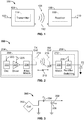
- FIG. 1 is a functional block diagram of an exemplary wireless power transfer system 100, in accordance with exemplary embodiments of the invention.
- Input power 102 may be provided to a transmitter 104 from a power source (not shown) for generating a field 105 for providing energy transfer.
- a receiver 108 may couple to the field 105 and generate output power 110 for storing or consumption by a device (not shown) coupled to the output power 110.
- Both the transmitter 104 and the receiver 108 are separated by a distance 112.
- transmitter 104 and receiver 108 are configured according to a mutual resonant relationship. When the resonant frequency of receiver 108 and the resonant frequency of transmitter 104 are substantially the same or very close, transmission losses between the transmitter 104 and the receiver 108 are minimal.
- wireless power transfer may be provided over larger distance in contrast to purely inductive solutions that may require large coils to be very close (e.g., mms).
- Resonant inductive coupling techniques may thus allow for improved efficiency and power transfer over various distances and with a variety of inductive coil configurations.
- the receiver 108 may receive power when the receiver 108 is located in an energy field 105 produced by the transmitter 104.
- the field 105 corresponds to a region where energy output by the transmitter 104 may be captured by a receiver 105. In some cases, the field 105 may correspond to the "near-field" of the transmitter 104 as will be further described below.
- the transmitter 104 may include a transmit antenna 114 for outputting an energy transmission.
- the receiver 108 further includes a receive antenna 118 for receiving or capturing energy from the energy transmission.
- the near-field may correspond to a region in which there are strong reactive fields resulting from the currents and charges in the transmit antenna 114 that minimally radiate power away from the transmit antenna 114.
- the near-field may correspond to a region that is within about one wavelength (or a fraction thereof) of the transmit antenna 114.
- the transmit and receive antennas 114 and 118 are sized according to applications and devices to be associated therewith. As described above, efficient energy transfer may occur by coupling a large portion of the energy in a field 105 of the transmit antenna 114 to a receive antenna 118 rather than propagating most of the energy in an electromagnetic wave to the far field. When positioned within the field 105, a "coupling mode" may be developed between the transmit antenna 114 and the receive antenna 118. The area around the transmit and receive antennas 114 and 118 where this coupling may occur is referred to herein as a coupling-mode region.
- FIG. 2 is a functional block diagram of exemplary components that may be used in the wireless power transfer system 100 of FIG. 1 , in accordance with various exemplary embodiments of the invention.
- the transmitter 204 may include transmit circuitry 206 that may include an oscillator 222, a driver circuit 224, and a filter and matching circuit 226.
- the oscillator 222 may be configured to generate a signal at a desired frequency, such as 468.75 KHz, 6.78 MHz or 13.56 MHz, that may be adjusted in response to a frequency control signal 223.
- the oscillator signal may be provided to a driver circuit 224 configured to drive the transmit antenna 214 at, for example, a resonant frequency of the transmit antenna 214.
- the driver circuit 224 may be a switching amplifier configured to receive a square wave from the oscillator 222 and output a sine wave.
- the driver circuit 224 may be a class E amplifier.
- a filter and matching circuit 226 may be also included to filter out harmonics or other unwanted frequencies and match the impedance of the transmitter 204 to the transmit antenna 214.
- the transmitter 204 may wirelessly output power at a level sufficient for charging or powering an electronic device.
- the power provided may be for example on the order of 300 milliWatts to 5 Watts to power or charge different devices with different power requirements. Higher or lower power levels may also be provided.
- the receiver 208 may include receive circuitry 210 that may include a matching circuit 232 and a rectifier and switching circuit 234 to generate a DC power output from an AC power input to charge a battery 236 as shown in FIG. 2 or to power a device (not shown) coupled to the receiver 108.
- the matching circuit 232 may be included to match the impedance of the receive circuitry 210 to the receive antenna 218.
- the receiver 208 and transmitter 204 may additionally communicate on a separate communication channel 219 (e.g., Bluetooth, zigbee, cellular, etc).
- the receiver 208 and transmitter 204 may alternatively communicate via in-band signaling using characteristics of the wireless field 206.
- receiver 208 may initially have a selectively disableable associated load (e.g., battery 236), may be configured to determine whether an amount of power transmitted by transmitter 204 and received by receiver 208 is appropriate for charging a battery 236. Further, receiver 208 may be configured to enable a load (e.g., battery 236) upon determining that the amount of power is appropriate. In some embodiments, a receiver 208 may be configured to directly utilize power received from a wireless power transfer field without charging of a battery 236.
- a selectively disableable associated load e.g., battery 236
- a communication device such as a near-field communication (NFC) or radio-frequency identification device (RFID may be configured to receive power from a wireless power transfer field and communicate by interacting with the wireless power transfer field and/or utilize the received power to communicate with a transmitter 204 or other devices.
- NFC near-field communication
- RFID radio-frequency identification device
- FIG. 3 is a schematic diagram of a portion of transmit circuitry 206 or receive circuitry 210 of FIG. 2 including a transmit or receive antenna 352, in accordance with exemplary embodiments of the invention.
- transmit or receive circuitry 350 used in exemplary embodiments including those described below may include an antenna 352.
- the antenna 352 may also be referred to or be configured as a "loop" antenna 352.
- the antenna 352 may also be referred to herein or be configured as a "magnetic" antenna or an induction coil.
- an antenna 352 is an example of a "power transfer component" of a type that is configured to wirelessly output and/or receive power.
- the antenna 352 may be configured to include an air core or a physical core such as a ferrite core (not shown). Air core loop antennas may be more tolerable to extraneous physical devices placed in the vicinity of the core. Furthermore, an air core loop antenna 352 allows the placement of other components within the core area. In addition, an air core loop may more readily enable placement of the receive antenna 218 ( FIG. 2 ) within a plane of the transmit antenna 214 ( FIG. 2 ) where the coupled-mode region of the transmit antenna 214 ( FIG. 2 ) may be more powerful.
- efficient transfer of energy between the transmitter 104 and receiver 108 may occur during matched or nearly matched resonance between the transmitter 104 and the receiver 108. However, even when resonance between the transmitter 104 and receiver 108 are not matched, energy may be transferred, although the efficiency may be affected. Transfer of energy occurs by coupling energy from the field 105 of the transmit antenna 214 coil to the receive antenna 218 residing in the neighborhood where this field 105 is established rather than propagating the energy from the transmit antenna 214 into free space.
- the resonant frequency of the loop or magnetic antennas is based on the inductance and capacitance.
- Inductance may be simply the inductance created by the antenna 352, whereas, capacitance may be added to the antenna's inductance to create a resonant structure at a desired resonant frequency.
- capacitor 352 and capacitor 354 may be added to the transmit or receive circuitry 350 to create a resonant circuit that selects a signal 356 at a resonant frequency. Accordingly, for larger diameter antennas, the size of capacitance needed to sustain resonance may decrease as the diameter or inductance of the loop increases. Furthermore, as the diameter of the antenna increases, the efficient energy transfer area of the near-field may increase.
- resonant circuits formed using other components are also possible.
- a capacitor may be placed in parallel between the two terminals of the antenna 350.
- a signal 358 with a frequency that substantially corresponds to the resonant frequency of the antenna 352 may be an input to the antenna 352.
- the transmitter 104 may be configured to output a time varying magnetic field with a frequency corresponding to the resonant frequency of the transmit antenna 114.
- the time varying magnetic field may induce a current in the receive antenna 118.
- the AC signal induced in the receive antenna 118 may be rectified as described above to produce a DC signal that may be provided to charge or to power a load.
- FIG. 4 is a functional block diagram of a transmitter 404 that may be used in the wireless power transfer system of FIG. 1 , in accordance with exemplary embodiments of the invention.
- the transmitter 404 may include transmit circuitry 406 and a transmit antenna 414.
- the transmit antenna 414 may be the antenna 352 as shown in FIG. 3 .
- Transmit circuitry 406 may provide RF power to the transmit antenna 414 by providing an oscillating signal resulting in generation of energy (e.g., magnetic flux) about the transmit antenna 414.
- Transmitter 404 may operate at any suitable frequency. By way of example, transmitter 404 may operate at the 6.78 MHz ISM band.
- Transmit circuitry 406 may include a fixed impedance matching circuit 409 for matching the impedance of the transmit circuitry 406 (e.g., 50 ohms) to the transmit antenna 414 and a low pass filter (LPF) 408 configured to reduce harmonic emissions to levels to prevent self-jamming of devices coupled to receivers 108 ( FIG. 1 ).
- LPF low pass filter
- Other exemplary embodiments may include different filter topologies, including but not limited to, notch filters that attenuate specific frequencies while passing others and may include an adaptive impedance match, that may be varied based on measurable transmit metrics, such as output power to the antenna 414 or DC current drawn by the driver circuit 424.
- Transmit circuitry 406 further includes a driver circuit 424 configured to drive an RF signal as determined by an oscillator 423.
- the transmit circuitry 406 may be comprised of discrete devices or circuits, or alternately, may be comprised of an integrated assembly.
- An exemplary RF power output from transmit antenna 414 may be on the order of 2.5 Watts.
- Transmit circuitry 406 may further include a controller 415 for selectively enabling the oscillator 423 during transmit phases (or duty cycles) for specific receivers, for adjusting the frequency or phase of the oscillator 423, and for adjusting the output power level for implementing a communication protocol for interacting with neighboring devices through their attached receivers. It is noted that the controller 415 may also be referred to herein as processor 415. Adjustment of oscillator phase and related circuitry in the transmission path may allow for reduction of out of band emissions, especially when transitioning from one frequency to another.
- the transmit circuitry 406 may further include a load sensing circuit 416 for detecting the presence or absence of active receivers in the vicinity of the near-field generated by transmit antenna 414.
- a load sensing circuit 416 monitors the current flowing to the driver circuit 424, that may be affected by the presence or absence of active receivers in the vicinity of the field generated by transmit antenna 414 as will be further described below. Detection of changes to the loading on the driver circuit 424 are monitored by controller 415 for use in determining whether to enable the oscillator 423 for transmitting energy and to communicate with an active receiver. As described more fully below, a current measured at the driver circuit 424 may be used to determine whether an invalid device is positioned within a wireless power transfer region of the transmitter 404.
- the transmit antenna 414 may be implemented with a Litz wire or as an antenna strip with the thickness, width and metal type selected to keep resistive losses low.
- the transmit antenna 414 may generally be configured for association with a larger structure such as a table, mat, lamp or other less portable configuration. Accordingly, the transmit antenna 414 generally may not need "turns" in order to be of a practical dimension.
- An exemplary implementation of a transmit antenna 414 may be "electrically small” (i.e., fraction of the wavelength) and tuned to resonate at lower usable frequencies by using capacitors to define the resonant frequency.
- the transmitter 404 may gather and track information about the whereabouts and status of receiver devices that may be associated with the transmitter 404.
- the transmit circuitry 406 may include a presence detector 480, an enclosed detector 460, or a combination thereof, connected to the controller 415 (also referred to as a processor herein).
- the controller 415 may adjust an amount of power delivered by the driver circuit 424 in response to presence signals from the presence detector 480 and the enclosed detector 460.
- the transmitter 404 may receive power through a number of power sources, such as, for example, an AC-DC converter (not shown) to convert conventional AC power present in a building, a DC-DC converter (not shown) to convert a conventional DC power source to a voltage suitable for the transmitter 404, or directly from a conventional DC power source (not shown).
- power sources such as, for example, an AC-DC converter (not shown) to convert conventional AC power present in a building, a DC-DC converter (not shown) to convert a conventional DC power source to a voltage suitable for the transmitter 404, or directly from a conventional DC power source (not shown).
- the presence detector 480 may be a motion detector utilized to sense the initial presence of a device to be charged that is inserted into the coverage area of the transmitter 404. After detection, the transmitter 404 may be turned on and the RF power received by the device may be used to toggle a switch on the Rx device in a pre-determined manner, which in turn results in changes to the driving point impedance of the transmitter 404.
- the presence detector 480 may be a detector capable of detecting a human, for example, by infrared detection, motion detection, or other suitable means.
- the controller 415 may adjust the power output of the transmit antenna 414 to a regulatory level or lower in response to human presence and adjust the power output of the transmit antenna 414 to a level above the regulatory level when a human is outside a regulatory distance from the electromagnetic field of the transmit antenna 414.
- the enclosed detector 460 may also be referred to herein as an enclosed compartment detector or an enclosed space detector
- the enclosed detector 460 may be a device such as a sense switch for determining when an enclosure is in a closed or open state.
- a power level of the transmitter may be increased.
- the load sensing circuit 416 may include circuitry configured to detect a dynamic impedance change resulting from a field that is applied or changed between transmit and receive coils of the transmitter 404 and a receiver (e.g., receiver 508 of FIG. 5 ), respectively, in response to the receiver being placed in a charging region of the transmitter 404.
- the load sensing circuit 416 may include circuitry configured to detect a change in impedance presented to the transmitter, the change resulting from a field that is applied to the charging region or changed between the transmit and receive coils, in response to the receiver being placed in the charging region.
- the load sensing circuit 416 may detect an impedance change pattern (not necessarily including a repeating waveform or shape) within a time interval and/or a type of impedance response within the time interval.
- the dynamic impedance change by recognizing a characteristic waveform associated with a charging of a capacitor (e.g., a filter capacitor) of the receiver during initial application of the field.
- the characteristic waveform may relate to or be based on the output impedance, the transmitter current, and/or the transmitter voltage.
- the characteristic waveform may include a transient spike in a transmitter current to the receiver.
- the load sensing circuit 416 may operate in conjunction with the controller 415 to switch the transmitter 404 from a power-save mode to a full-charging mode, in response to the receiver being in the charging region.
- the load sensing circuit 416 or the like may operate in conjunction with one or more components of the transmitter 404, illustrated or otherwise. In further related aspects, the load sensing circuit 416 or the like may be configured to detect placement of the receiver in the charging region of the 404 transmitter according to the features described in further detail below with reference to FIGs. 7A-13 .
- a method by which the transmitter 404 does not remain on indefinitely may be used.
- the transmitter 404 may be programmed to shut off after a user-determined amount of time. This feature prevents the transmitter 404, notably the driver circuit 424, from running long after the wireless devices in its perimeter are fully charged. This event may be due to the failure of the circuit to detect the signal sent from either the repeater or the receive antenna 218 that a device is fully charged.
- the transmitter 404 automatic shut off feature may be activated only after a set period of lack of motion detected in its perimeter. The user may be able to determine the inactivity time interval, and change it as desired. As a non-limiting example, the time interval may be longer than that needed to fully charge a specific type of wireless device under the assumption of the device being initially fully discharged.
- FIG. 5 is a functional block diagram of a receiver 508 that may be used in the wireless power transfer system of FIG. 1 , in accordance with exemplary embodiments of the invention.
- the receiver 508 includes receive circuitry 510 that may include a receive antenna 518. Receiver 508 further couples to device 550 for providing received power thereto. It should be noted that receiver 508 is illustrated as being external to device 550 but may be integrated into device 550. Energy may be propagated wirelessly to receive antenna 518 and then coupled through the rest of the receive circuitry 510 to device 550.
- the charging device may include devices such as mobile phones, portable music players, laptop computers, tablet computers, computer peripheral devices, communication devices (e.g., Bluetooth devices), digital cameras, hearing aids (or other medical devices), and the like.
- Receive antenna 518 may be tuned to resonate at the same frequency, or within a specified range of frequencies, as transmit antenna 414 ( FIG. 4 ). Receive antenna 518 may be similarly dimensioned with transmit antenna 414 or may be differently sized based upon the dimensions of the associated device 550.
- device 550 may be a portable electronic device having diametric or length dimension smaller than the diameter or length of transmit antenna 414.
- receive antenna 518 may be implemented as a multi-turn coil in order to reduce the capacitance value of a tuning capacitor (not shown) and increase the receive coil's impedance.
- receive antenna 518 may be placed around the substantial circumference of device 550 in order to maximize the antenna diameter and reduce the number of loop turns (i.e., windings) of the receive antenna 518 and the inter-winding capacitance.
- Receive circuitry 510 may provide an impedance match to the receive antenna 518.
- Receive circuitry 510 includes power conversion circuitry 506 for converting a received RF energy source into charging power for use by the device 550.
- Power conversion circuitry 506 includes an RF-to-DC converter 520 and may also include a DC-to-DC converter 522.
- RF-to-DC converter 520 rectifies the RF energy signal received at receive antenna 518 into a non-alternating power with an output voltage represented by V rect .
- the DC-to-DC converter 522 (or other power regulator) converts the rectified RF energy signal into an energy potential (e.g., voltage) that is compatible with device 550 with an output voltage and output current represented by V out and I out .
- Various RF-to-DC converters are contemplated, including partial and full rectifiers, regulators, bridges, doublers, as well as linear and switching converters.
- Receive circuitry 510 may further include switching circuitry 512 for connecting receive antenna 518 to the power conversion circuitry 506 or alternatively for disconnecting the power conversion circuitry 506. Disconnecting receive antenna 518 from power conversion circuitry 506 not only suspends charging of device 550, but also changes the "load” as “seen” by the transmitter 404 ( FIG. 2 ).
- transmitter 404 includes load sensing circuit 416 that may detect fluctuations in the bias current provided to transmitter driver circuit 424. Accordingly, transmitter 404 has a mechanism for determining when receivers are present in the transmitter's near-field.
- a receiver 508 When multiple receivers 508 are present in a transmitter's near-field, it may be desirable to time-multiplex the loading and unloading of one or more receivers to enable other receivers to more efficiently couple to the transmitter.
- a receiver 508 may also be cloaked in order to eliminate coupling to other nearby receivers or to reduce loading on nearby transmitters. This "unloading" of a receiver is also known herein as a “cloaking.”
- this switching between unloading and loading controlled by receiver 508 and detected by transmitter 404 may provide a communication mechanism from receiver 508 to transmitter 404 as is explained more fully below.
- a protocol may be associated with the switching that enables the sending of a message from receiver 508 to transmitter 404.
- a switching speed may be on the order of 100 ⁇ sec.
- communication between the transmitter 404 and the receiver 508 refers to a device sensing and charging control mechanism, rather than conventional two-way communication (i.e., in band signaling using the coupling field).
- the transmitter 404 may use on/off keying of the transmitted signal to adjust whether energy is available in the near-field.
- the receiver may interpret these changes in energy as a message from the transmitter 404.
- the receiver 508 may use tuning and de-tuning of the receive antenna 518 to adjust how much power is being accepted from the field. In some cases, the tuning and de-tuning may be accomplished via the switching circuitry 512.
- the transmitter 404 may detect this difference in power used from the field and interpret these changes as a message from the receiver 508. It is noted that other forms of modulation of the transmit power and the load behavior may be utilized.
- Receive circuitry 510 may further include signaling detector and beacon circuitry 514 used to identify received energy fluctuations that may correspond to informational signaling from the transmitter to the receiver. Furthermore, signaling and beacon circuitry 514 may also be used to detect the transmission of a reduced RF signal energy (i.e., a beacon signal) and to rectify the reduced RF signal energy into a nominal power for awakening either un-powered or power-depleted circuits within receive circuitry 510 in order to configure receive circuitry 510 for wireless charging.
- a reduced RF signal energy i.e., a beacon signal
- Receive circuitry 510 further includes processor 516 for coordinating the processes of receiver 508 described herein including the control of switching circuitry 512 described herein. Cloaking of receiver 508 may also occur upon the occurrence of other events including detection of an external wired charging source (e.g., wall/USB power) providing charging power to device 550.
- Processor 516 in addition to controlling the cloaking of the receiver, may also monitor beacon circuitry 514 to determine a beacon state and extract messages sent from the transmitter 404. Processor 516 may also adjust the DC-to-DC converter 522 for improved performance.
- FIG. 6 is a schematic diagram of a portion of transmit circuitry 600 that may be used in the transmit circuitry 406 of FIG. 4 .
- the transmit circuitry 600 may include a driver circuit 624 as described above in FIG. 4 .
- the driver circuit 624 may be a switching amplifier that may be configured to receive a square wave and output a sine wave to be provided to the transmit circuit 650. In some cases the driver circuit 624 may be referred to as an amplifier circuit.
- the driver circuit 624 is shown as a class E amplifier; however, any suitable driver circuit 624 may be used in accordance with embodiments of the invention.
- the driver circuit 624 may be driven by an input signal 602 from an oscillator 423 as shown in FIG. 4 .
- the driver circuit 624 may also be provided with a drive voltage V D that is configured to control the maximum power that may be delivered through a transmit circuit 650.
- the transmit circuitry 600 may include a filter circuit 626.
- the filter circuit 626 may be a three pole (capacitor 634, inductor 632, and capacitor 636) low pass filter circuit 626.
- the signal output by the filter circuit 626 may be provided to a transmit circuit 650 comprising an antenna 614.
- the transmit circuit 650 may include a series resonant circuit having a capacitance 620 and inductance (e.g., that may be due to the inductance or capacitance of the antenna or to an additional capacitor component) that may resonate at a frequency of the filtered signal provided by the driver circuit 624.
- the load of the transmit circuit 650 may be represented by the variable resistor 622.
- the load may be a function of a wireless power receiver 508 that is positioned to receive power from the transmit circuit 650.
- a wireless power transmitter such as, for example, a charging pad.
- a wireless power transmitter such as, for example, a charging pad.
- Some wireless chargers go to a lower power state when there are no devices on the charging pad. This reduces quiescent power dissipation, which in turn increases overall efficiency, such as, for example, over the course of several days.
- the charger pad when the charger pad is in this lower power state, it can be more difficult to detect devices being placed in the charging region, since the RF energy may be absent, absent for most of the time, or at a much lower level than when the charger pad is turned on. This means a user might place a device on a pad and have the charger pad not turn back on, or take a long time to turn back on. This may result in a delay in charging and a poor user experience.
- impedance may refer to both the real impedance (resistance) and/or the imaginary impedance (reactance).
- the system may be configured to detect or observe a change in either type of impedance for purposes of powering on when the device is place in the charging region.
- While the above-described approach may work in many cases, there are situations where issues may arise. For example, a small device placed on a large charging pad may not generate enough of an impedance change to signal or trigger the charging pad to begin charging. In another example, certain designs of the charging pad (or the receiving device) may be specifically intended to minimize impedance change in order to improve efficiency. In yet another example, foreign objects (e.g., coins, keys, etc.) on the charger pad may cause a reactance shift, which may cause the system to begin charging without the device in the charging region.
- foreign objects e.g., coins, keys, etc.
- Wireless power receivers include rectification and filtering to transform received RF energy back to useful DC power.
- the filter capacitor may present a much lower impedance than would be detected during steady state operation.
- the effect of this temporary lower impedance can be detected and used to determine, for example, whether a device has been placed on a charging pad.
- the much lower impedance of the filter capacitor of the power receiving device at initial power-on, relative to at steady state operation may result in a measurable or detectable effect in the form of a transient or short term impedance change.
- FIG. 7 provides a simplified schematic of an example wireless power system 700 with the transmitter 710 is on the left side and the receiver 720 on the right side.
- the transmitter 710 includes a power amplifier (PA) 712 (corresponding to the switching amplifier of the driver circuit 624 in FIG. 6 ) coupled to a capacitor 714 (corresponding to the capacitor 620 of the transmit circuit 650 in FIG. 6 , which is in turn coupled to an inductor 716 (corresponding to the inductor 614 of the transmit circuit 650 in FIG. 6 ), wherein the capacitor 714 and inductor 716 may collectively function as or correspond to the series resonant circuit having a capacitance 620 and inductor 614 that may resonate at a frequency of the filtered signal provided by the driver circuit 624 in FIG. 6 .
- the capacitor 714 and the inductor 716 of the transmitter 710 form a resonant circuit where the inductor 716 may be formed of a coil used to generate a magnetic field for coupling wireless power to the receiver 720.
- the receiver 720 includes an inductor 722 (which may be formed of a coil and coupled to and receive wireless power from the inductor 716 and may correspond to the antenna 518 of the receiver 500 in FIG. 5 ) coupled to a capacitor 724 (corresponding to the capacitor 354 or the capacitor 356 in FIG. 3 ), wherein the inductor 722 and the capacitor 724 form a resonant circuit at the receiver 720 and determine the resonant frequency of the resonant circuit.
- the resonant frequency is in turn coupled to diodes 726, 728 of a rectifier.
- the cathode of the diode 728 and the anode of diode 728 are coupled to a capacitor C RECT 730.
- the diodes 726, 728 and the capacitor C RECT 730 may form or be part of an RF-to-DC converter (correspond to the RF-to-DC converter 520 of the power conversion circuitry 506 in FIG. 5 ).
- the capacitor C RECT 730 in turn may be coupled in parallel to R LOAD 732.
- Z OUTPUT corresponds to the output impedance observed by the PA 712 looking into the rectifier.
- FIG. 8 shows an even more simplified representation of a wireless charging circuit 800, in which the coupling and losses in the transmit and receive resonators are shown as resistances R TX 810 and R RX 820.
- a diode 830 is coupled to a capacitor C RECT 730.
- the remaining circuit components are similar to those described above with reference to FIG. 7 . It is noted that the combination of resistances and the capacitor may form an RC network with a predictable time constant. When looking into this RC network from the amplifier on the left, the observed impedance will start out low and then rise as the capacitor begins to charge.
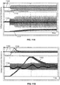
- FIG. 9A The effect of the observed impedance starting out low and then rising is shown in FIG. 9A .
- the PA When the PA first turns on in the case of the empty pad, normally the PA sees the same impedance with time. Resistance is sensed to be a specific value that does not change. In the case of a foreign object on the pad, the sensed resistance may be different but remain unchanging or constant. It is noted that complex impedance includes both resistance and reactance, wherein the resistance and/or reactance values can change.
- a wireless power receiver is on the pad when the amplifier turns on. Due to the capacitor taking a finite amount of time to charge, the impedance starts out low, then ramps up to the final steady state value.
- a system, or component(s) thereof may be configured to observe these specific type or pattern of responses and determine that the case in FIG. 9A does not represent a valid device on the pad, and that the system should remain in the low power state. In the alternative, or in addition, the system, or component(s) thereof, may be configured to determine that the case in FIG. 9B represents a valid device on the pad, and that the system should transition from a low power state to a full power/charging state.
- the transmitter may not be able to directly measure output impedance.
- the system, or component(s) thereof may be configured to measure proxy values, such as, for example, the transmitter PA input current, transmitter PA input voltage, or the like.
- proxy values such as, for example, the transmitter PA input current, transmitter PA input voltage, or the like.
- FIG. 10A illustrates the transmitter current over time for an example case where the power receiving device is not in the charging region of the charging pad.
- FIG. 10B illustrates the transmitter current over time for an example case where the transmitter current is delivered to the power receiving device in the charging region.
- a system, or component(s) thereof may be configured to observe these specific type or pattern of responses and determine that the case in FIG. 10A does not represent a valid device on the pad, and that the system should remain in the low power state.
- the system, or component(s) thereof may be configured to determine that the case in FIG. 10B represents a valid device on the pad, and that the system should transition from a low power state to a full power/charging state.
- FIG. 11A shows example test measurements of the transmitter's PA input current 1110, 1112 and AC coupled PA input voltage 1120, 1122 for an empty charging pad. Traces 1112 and 1122 correspond to a zoomed in view of traces 1110 and 1120, respectively. It is noted that the current rises to a final value. The delay here is caused by the low bandwidth of the current sense circuitry.
- FIG. 11B shows example measurements of the transmitter's current 1130, 1132 and voltage 1140, 1142 when a wireless device has been placed on the charging pad. Traces 1132 and 1142 correspond to a zoomed in view of traces 1130 and 1140, respectively. It is noted that the initial spike in current is due to the low impedance caused by the charging capacitor.
- FIGs. 12A-B the transmitter's PA input current 1210, 1212 and AC coupled PA input voltage 1220, 1222 are again measured. Traces 1212 and 1222 correspond to a zoomed in view of traces 1210 and 1220, respectively.
- a rogue device e.g., could be a metal object or some other device without appropriate receive circuitry
- the rogue device has been simulated by using a wireless power receiver with its rectifier and capacitor disconnected. As such, the rogue device "appears" as an open circuit.
- the rogue device example of FIG. 12A looks very similar to the empty pad case of FIG. 11A . In such as case, a valid device would not be detected.
- FIG. 12A looks very similar to the empty pad case of FIG. 11A . In such as case, a valid device would not be detected.
- FIG. 12A looks very similar to the empty pad case of FIG. 11A . In such as case, a valid device would not be detected.
- FIG. 12A looks very
- Traces 1232 and 1242 correspond to a zoomed in view of traces 1230 and 1240, respectively.
- the initial spike in current due to the low impedance is caused by the charging capacitor.
- a characteristic waveform with such a spike allows for and facilitates the detection of a valid device.
- FIG. 13 is a functional block diagram of a device 1300 for detecting placement of a wireless power receiver in a charging region of a wireless power transmitter, in accordance with an exemplary embodiment of the disclosure.
- the device 1300 may include a transmit circuit 1310 comprising a transmit coil 1312 and configured to wirelessly transmit power to a receive coil of the receiver.
- the transmit circuit 1310 may include one or more components of the transmitter 404 of FIG. 4 and/or the transmit circuitry 600 of FIG. 6 , the details of which are provided in further detail above.
- the transmit circuit 1310 may include a low power beacon transmitter 1314 for detecting changes in the output impedance caused by placement of an object in a charging region of the transmit circuit 1310, while reducing standby power.
- the beacon transmitter 1314 may be configured to periodically apply a short beacon to a resonator of the transmit circuit 1310 to detect changes in impedance. With the short beacon, the device 1300 shall be capable of sensing the reactance and/or resistance change of the detected output impedance.
- the low power beacon transmitter 1314 may be further configured to initiate a higher power state upon detecting a load variation with the short beacon.
- the transmitter 1314 may be configured to apply a "long" beacon that may be longer or have higher power than the short beacon.
- the "long" beacon may provide sufficient power to the receiver to allow the receiver to have enough power to establish communication with transmitter to allow the transmitter 1314 to initiate higher power states.
- the beacon transmitter 1314 may be part of a detection circuit 1320 (described below) rather than the transmit circuit 1310.
- the beacon transmitter 1314 may be a separate low power transmitter, or alternatively may be the primary power transmitter operated at a lower power.
- the device 1300 may also include a detection circuit 1320 configured to detect a change in impedance presented to the transmitter, the change resulting from a field that is applied to the charging region or changed between the transmit and receive coils, in response to the receiver being placed in the charging region.
- the detection circuit 1320 may correspond to or include the load sensing circuit 416 or the like of the transmitter 404 of FIG. 4 , the details of which are provided in further detail above.
- the detection circuit 1320 may include a waveform detector 1322 for recognizing a characteristic waveform (e.g., including a transient spike in the transmitter current to the receiver) associated with a charging of a capacitor (e.g., filter capacitor) of the receiver during initial application of the field.
- a characteristic waveform e.g., including a transient spike in the transmitter current to the receiver
- a capacitor e.g., filter capacitor
- the waveform may relate to or be based on the output impedance, the transmitter current, and/or the transmitter voltage. More generally, the detection circuit 1320 may be configured to detect an impedance change pattern or a type of impedance response (e.g., either via impedance or current response measurements) within a given time interval or period. The time interval/period for detecting a specific type of impedance change/waveform may occur during the short beacon.
- the detection circuit 1320 may include a slope detector circuit 1324 for detecting a slope of the measured output impedance (e.g., the trace in FIG. 9B ) or the like.
- the detection circuit 1320 may include a dedicated processor 1326 that may optionally have digital signal processing 1328 programmed into it to sample the waveform(s) and perform any processing/filtering to determine signal parameters in the sampled waveform(s).
- the above processing tasks may share the resources of an existing processor.
- the beacon transmitter 1314 may be part of the detection circuit 1320 rather than the transmit circuit 1310.
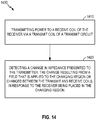
- FIG. 14 provides a flowchart of an exemplary method 1400 for wireless charging, and more particularly for detecting placement of a wireless power receiver in a charging region of a wireless power transmitter, in accordance with one or more aspects of the present disclosure.
- the method 1400 is described herein with reference to a particular order, in various implementations, the step(s) or feature(s) herein may be performed in a different order, or may be omitted, or may include additional step(s)/features(s).
- the method 1400 may be operable by a wireless power transmitter (e.g., the device 1300 of FIG. 13 ) or component(s) thereof.
- the method 1400 may involve, at 1410, transmitting power via a wireless field applied to the charging region to a receive coil of the receiver via a transmit coil of a transmit circuit.
- block 1410 may be performed by the transmit circuit 1310 of FIG. 13 or component(s) thereof.
- the method 1400 may involve, at 1420, detecting a characteristic waveform resulting from the field that is applied to the charging region or changed between the transmit and receive coils, in response to the receiver being placed in the charging region.
- block 1420 may be performed by the detection circuit 1320 of FIG. 13 or component(s) thereof.
- the characteristic waveform may be associated with a charging of a capacitor of the receiver during initial application of the field, and may be based at least in part on a change in impedance presented to the transmit circuit of the transmitter in response to the receiver being placed in the charging region.
- block 1420 may involve, at 1430, recognizing an impedance pattern change associated with a charging of a capacitor of the receiver during initial application of the field.
- the characteristic waveform may comprise a transient spike in resistance as calculated based on a transmitter voltage and a transmitter current
- the transmitter voltage may comprise an AC voltage and the transmitter current comprises an AC current
- block 1420 may involve, at 1440, measuring the AC voltage and the AC current at substantially a same point in an AC path.
- block 1420 may involve, at 1450, measuring the AC current at a first point in an AC path, the AC current having a known relation to, in at least one of amplitude or phase, a corresponding AC current measured at a second point in the AC path where the AC voltage is measured.
- the characteristic waveform may comprise a transient spike in resistance as calculated based on a transmitter voltage and a transmitter current
- the transmitter voltage may comprise a DC voltage
- the transmitter current comprises a DC current
- block 1420 may involve, at 1460, measuring the DC current at a first point in a DC path, the DC current having a known relation in value to a corresponding DC current measured at a second point where the DC voltage is measured.
- the method 1400 may further involve, at 1470, switching the transmitter from a power-save mode to a higher power mode, in response to the receiver being in the charging region.
- means for transmitting power via a wireless field applied to the charging region to a receive coil of the receiver may comprise, for example, a transmit coil, a beacon transmitter, a power amplifier, and/or other component(s) of a transmit circuit.
- means for detecting a characteristic waveform in response to the receiver being placed in the charging region, may comprise, for example: a load sensing circuit; a waveform detector for recognizing a characteristic waveform associated with a charging of a capacitor of the receiver during initial application of the field; a slope detector for detecting a slope of a measured output impedance; a dedicated processor/controller; and/or other component(s) of a detection circuit.
- means for detecting the characteristic waveform or recognizing an impedance change pattern associated with a charging of a capacitor of the receiver during initial application of the field may comprise, for example, a waveform detector for recognizing a characteristic waveform or pattern (e.g., including a transient spike in the transmitter current to the receiver) associated with a charging of a capacitor of the receiver during initial application of the field.
- a waveform detector for recognizing a characteristic waveform or pattern (e.g., including a transient spike in the transmitter current to the receiver) associated with a charging of a capacitor of the receiver during initial application of the field.
- means for measuring the AC voltage and the AC current at substantially a same point in an AC path may comprise, for example, a load sensing circuit, a waveform detector, a slope detector, a processor/controller, and/or other component(s) of a detection circuit.
- means for measuring the AC current at a first point in an AC path may comprise, for example, a load sensing circuit, a waveform detector, a slope detector, a processor/controller, and/or other component(s) of a detection circuit.
- Information and signals may be represented using any of a variety of different technologies and techniques.
- data, instructions, commands, information, signals, bits, symbols, and chips that may be referenced throughout the above description may be represented by voltages, currents, electromagnetic waves, magnetic fields or particles, optical fields or particles, or any combination thereof.
- DSP Digital Signal Processor
- ASIC Application Specific Integrated Circuit
- FPGA Field Programmable Gate Array
- a general purpose processor may be a microprocessor, but in the alternative, the processor may be any conventional processor, controller, microcontroller, or state machine.
- a processor may also be implemented as a combination of computing devices, e.g., a combination of a DSP and a microprocessor, a plurality of microprocessors, one or more microprocessors in conjunction with a DSP core, or any other such configuration.
- a software module may reside in Random Access Memory (RAM), flash memory, Read Only Memory (ROM), Electrically Programmable ROM (EPROM), Electrically Erasable Programmable ROM (EEPROM), registers, hard disk, a removable disk, a CD ROM, or any other form of storage medium known in the art.
- RAM Random Access Memory
- ROM Read Only Memory
- EPROM Electrically Programmable ROM
- EEPROM Electrically Erasable Programmable ROM
- registers hard disk, a removable disk, a CD ROM, or any other form of storage medium known in the art.
- a storage medium is coupled to the processor such that the processor can read information from, and write information to, the storage medium.
- the storage medium may be integral to the processor.
- Disk and disc includes compact disc (CD), laser disc, optical disc, digital versatile disc (DVD), floppy disk and blu ray disc where disks usually reproduce data magnetically, while discs reproduce data optically with lasers. Combinations of the above should also be included within the scope of computer readable media.
- the processor and the storage medium may reside in an ASIC.
- the ASIC may reside in a user terminal.
- the processor and the storage medium may reside as discrete components in a user terminal.
Claims (14)
- Drahtloser Leistungssender (1300) zum Erfassen der Anordnung eines drahtlosen Leistungsempfängers in einem Ladebereich des drahtlosen Leistungssenders, umfassend:eine Sendeschaltung (1310), die eine Sendespule umfasst und konfiguriert ist, um Leistung drahtlos über ein drahtloses Feld zu übertragen, das an den Ladebereich an eine Empfangsspule des Empfängers angelegt ist; undeine Erfassungsschaltung (1320), die konfiguriert ist, um eine Charakteristik einer Wellenform zu erfassen, die sich aus dem Feld ergibt, das zwischen den Sende- und Empfangsspulen angelegt oder geändert wird, als Reaktion darauf, dass der Empfänger in dem Ladebereich platziert wird;dadurch gekennzeichnet dass, die Charakteristik der Wellenform ein messbarer Effekt eines transienten oder kurzfristigen Impedanzänderungsmusters innerhalb eines Zeitintervalls ist, das einem Laden eines Kondensators des Empfängers während der ersten Anwendung des Feldes zugeordnet ist.
- Drahtloser Leistungssender (1300) nach Anspruch 1, wobei die Charakteristik der Wellenform dem Laden eines Kondensators des Empfängers während der anfänglichen Anwendung des Feldes zugeordnet ist und zumindest teilweise auf einer Änderung der Impedanz basiert, die der Sendeschaltung des Senders als Reaktion darauf präsentiert wird, dass der Empfänger in dem Ladebereich platziert wird.
- Drahtloser Leistungssender (1300) nach Anspruch 1, wobei die Charakteristik der Wellenform eine transiente Spitze in einem Senderstrom umfasst.
- Drahtloser Leistungssender (1300) nach Anspruch 3, wobei der Senderstrom einen Gleichstrom in einen Leistungsverstärker, PA, des Senders umfasst.
- Drahtloser Leistungssender (1300) nach Anspruch 1, wobei die Charakteristik der Wellenform eine transiente Spitze oder Schwingung in einer Senderspannung umfasst.
- Drahtloser Leistungssender (1300) nach Anspruch 1, wobei die Erfassungsschaltung ferner konfiguriert ist, um den Sender von einem Energiesparmodus in einen höheren Leistungsmodus zu schalten, als Reaktion darauf, dass sich der Empfänger im Ladebereich befindet.
- Drahtloser Leistungssender (1300) nach Anspruch 1, wobei die Erfassungsschaltung ferner konfiguriert ist, um eine Änderung der Impedanz zu erfassen, die dem Sender als Reaktion darauf, dass ein gültiger Empfänger in dem Ladebereich angeordnet ist, präsentiert wird, wobei der gültige Empfänger eine Empfängerschaltung mit einem Gleichrichter und dem Kondensator in verbundenen Zuständen umfasst, wobei der Kondensator konfiguriert ist, um während der ersten Anwendung des Feldes aufzuladen.
- Verfahren (1400) zum Erfassen der Anordnung eines drahtlosen Leistungsempfängers in einem Ladebereich eines drahtlosen Leistungssenders, umfassend:Übertragen (1410) von Leistung über ein drahtloses Feld, das an den Ladebereich angelegt ist, an eine Empfangsspule des Empfängers über eine Sendespule einer Sendeschaltung; undErfassen (1420) einer Charakteristik einer Wellenform, die sich aus dem Feld ergibt, das zwischen den Sende- und Empfangsspulen angelegt oder geändert wird, als Reaktion darauf, dass der Empfänger in dem Ladebereich platziert wird;dadurch gekennzeichnet dass, die Charakteristik der Wellenform ein messbarer Effekt eines transienten oder kurzfristigen Impedanzänderungsmusters innerhalb eines Zeitintervalls ist, das einem Laden eines Kondensators des Empfängers während der ersten Anwendung des Feldes zugeordnet ist.
- Verfahren (1400) nach Anspruch 8, worin die Charakteristik der Wellenform einen transienten Anstieg der Impedanz umfasst, wie er basierend auf einer Senderspannung und einem Senderstrom berechnet wird.
- Verfahren (1400) nach Anspruch 9, worin die Senderspannung eine Wechselspannung und der Senderstrom einen Wechselstrom umfasst, und das Erfassen der Charakteristik der Wellenform das Messen der Wechselspannung und des Wechselstroms an im Wesentlichen demselben Punkt in einem Wechselstrompfad umfasst.
- Verfahren (1400) nach Anspruch 9, wobei das Erfassen der Charakteristik der Wellenform das Messen des Wechselstroms an einem ersten Punkt in einem Wechselstrompfad umfasst, wobei der Wechselstrom eine bekannte Beziehung zu einem entsprechenden Wechselstrom aufweist, der an einem zweiten Punkt in dem Wechselstrompfad gemessen wird, an dem die Wechselspannung gemessen wird, in mindestens einer Amplitude oder Phase.
- Verfahren (1400) nach Anspruch 8, wobei:die Charakteristik der Wellenform einen transienten Anstieg der Impedanz umfasst, wie er basierend auf einer Senderspannung und einem Senderstrom berechnet wird.
- Computerprogramm, umfassend Anweisungen zum Ausführen eines Verfahrens nach einem der Ansprüche 8 bis 12, wenn es auf einem Computer ausgeführt wird.
- Computerlesbares Speichermedium, umfassend das Computerprogramm nach Anspruch 13.
Applications Claiming Priority (3)
| Application Number | Priority Date | Filing Date | Title |
|---|---|---|---|
| US201461940254P | 2014-02-14 | 2014-02-14 | |
| US14/486,690 US9995777B2 (en) | 2014-02-14 | 2014-09-15 | Device detection through dynamic impedance change measurement |
| PCT/US2015/014853 WO2015123110A1 (en) | 2014-02-14 | 2015-02-06 | Device detection through dynamic impedance change measurement |
Publications (2)
| Publication Number | Publication Date |
|---|---|
| EP3108565A1 EP3108565A1 (de) | 2016-12-28 |
| EP3108565B1 true EP3108565B1 (de) | 2018-12-05 |
Family
ID=53797929
Family Applications (1)
| Application Number | Title | Priority Date | Filing Date |
|---|---|---|---|
| EP15704927.1A Active EP3108565B1 (de) | 2014-02-14 | 2015-02-06 | Vorrichtungserkennung durch dynamische impedanzänderungsmessung |
Country Status (6)
| Country | Link |
|---|---|
| US (1) | US9995777B2 (de) |
| EP (1) | EP3108565B1 (de) |
| JP (1) | JP6542244B2 (de) |
| KR (1) | KR20160122789A (de) |
| CN (1) | CN105993105B (de) |
| WO (1) | WO2015123110A1 (de) |
Families Citing this family (94)
| Publication number | Priority date | Publication date | Assignee | Title |
|---|---|---|---|---|
| US10038338B2 (en) | 2011-02-01 | 2018-07-31 | Fu Da Tong Technology Co., Ltd. | Signal modulation method and signal rectification and modulation device |
| US10951063B2 (en) | 2011-02-01 | 2021-03-16 | Fu Da Tong Technology Co., Ltd. | Supplying-end module of induction type power supply system and signal detection method thereof |
| US10630116B2 (en) | 2011-02-01 | 2020-04-21 | Fu Da Tong Technology Co., Ltd. | Intruding metal detection method for induction type power supply system and related supplying-end module |
| US10312748B2 (en) | 2011-02-01 | 2019-06-04 | Fu Da Tong Techology Co., Ltd. | Signal analysis method and circuit |
| US11128180B2 (en) | 2011-02-01 | 2021-09-21 | Fu Da Tong Technology Co., Ltd. | Method and supplying-end module for detecting receiving-end module |
| US10289142B2 (en) * | 2011-02-01 | 2019-05-14 | Fu Da Tong Technology Co., Ltd. | Induction type power supply system and intruding metal detection method thereof |
| US10574095B2 (en) | 2011-02-01 | 2020-02-25 | Fu Da Tong Technology Co., Ltd. | Decoding method for signal processing circuit and signal processing circuit using the same |
| US10673287B2 (en) | 2011-02-01 | 2020-06-02 | Fu Da Tong Technology Co., Ltd. | Method and supplying-end module for detecting receiving-end module |
| US10587153B2 (en) | 2011-02-01 | 2020-03-10 | Fu Da Tong Technology Co., Ltd. | Intruding metal detection method for induction type power supply system and related supplying-end module |
| US11502551B2 (en) | 2012-07-06 | 2022-11-15 | Energous Corporation | Wirelessly charging multiple wireless-power receivers using different subsets of an antenna array to focus energy at different locations |
| US10992185B2 (en) | 2012-07-06 | 2021-04-27 | Energous Corporation | Systems and methods of using electromagnetic waves to wirelessly deliver power to game controllers |
| US9871398B1 (en) | 2013-07-01 | 2018-01-16 | Energous Corporation | Hybrid charging method for wireless power transmission based on pocket-forming |
| US10439448B2 (en) | 2014-08-21 | 2019-10-08 | Energous Corporation | Systems and methods for automatically testing the communication between wireless power transmitter and wireless power receiver |
| US9812890B1 (en) | 2013-07-11 | 2017-11-07 | Energous Corporation | Portable wireless charging pad |
| US10992187B2 (en) | 2012-07-06 | 2021-04-27 | Energous Corporation | System and methods of using electromagnetic waves to wirelessly deliver power to electronic devices |
| US9853458B1 (en) | 2014-05-07 | 2017-12-26 | Energous Corporation | Systems and methods for device and power receiver pairing |
| US10124754B1 (en) | 2013-07-19 | 2018-11-13 | Energous Corporation | Wireless charging and powering of electronic sensors in a vehicle |
| US9876394B1 (en) | 2014-05-07 | 2018-01-23 | Energous Corporation | Boost-charger-boost system for enhanced power delivery |
| US10965164B2 (en) | 2012-07-06 | 2021-03-30 | Energous Corporation | Systems and methods of wirelessly delivering power to a receiver device |
| US10063105B2 (en) | 2013-07-11 | 2018-08-28 | Energous Corporation | Proximity transmitters for wireless power charging systems |
| US10381880B2 (en) | 2014-07-21 | 2019-08-13 | Energous Corporation | Integrated antenna structure arrays for wireless power transmission |
| US10256657B2 (en) | 2015-12-24 | 2019-04-09 | Energous Corporation | Antenna having coaxial structure for near field wireless power charging |
| US9867062B1 (en) | 2014-07-21 | 2018-01-09 | Energous Corporation | System and methods for using a remote server to authorize a receiving device that has requested wireless power and to determine whether another receiving device should request wireless power in a wireless power transmission system |
| US9887584B1 (en) | 2014-08-21 | 2018-02-06 | Energous Corporation | Systems and methods for a configuration web service to provide configuration of a wireless power transmitter within a wireless power transmission system |
| US9787103B1 (en) | 2013-08-06 | 2017-10-10 | Energous Corporation | Systems and methods for wirelessly delivering power to electronic devices that are unable to communicate with a transmitter |
| US9806564B2 (en) | 2014-05-07 | 2017-10-31 | Energous Corporation | Integrated rectifier and boost converter for wireless power transmission |
| US20150229135A1 (en) * | 2014-02-10 | 2015-08-13 | Shahar Porat | Wireless load modulation |
| US10068703B1 (en) | 2014-07-21 | 2018-09-04 | Energous Corporation | Integrated miniature PIFA with artificial magnetic conductor metamaterials |
| US10523033B2 (en) | 2015-09-15 | 2019-12-31 | Energous Corporation | Receiver devices configured to determine location within a transmission field |
| US9871387B1 (en) | 2015-09-16 | 2018-01-16 | Energous Corporation | Systems and methods of object detection using one or more video cameras in wireless power charging systems |
| US10778041B2 (en) | 2015-09-16 | 2020-09-15 | Energous Corporation | Systems and methods for generating power waves in a wireless power transmission system |
| US10186893B2 (en) | 2015-09-16 | 2019-01-22 | Energous Corporation | Systems and methods for real time or near real time wireless communications between a wireless power transmitter and a wireless power receiver |
| US10211685B2 (en) | 2015-09-16 | 2019-02-19 | Energous Corporation | Systems and methods for real or near real time wireless communications between a wireless power transmitter and a wireless power receiver |
| US10199850B2 (en) | 2015-09-16 | 2019-02-05 | Energous Corporation | Systems and methods for wirelessly transmitting power from a transmitter to a receiver by determining refined locations of the receiver in a segmented transmission field associated with the transmitter |
| KR102483302B1 (ko) * | 2015-09-18 | 2022-12-30 | 삼성전자주식회사 | 무선 전력 송신기, 무선 전력 수신기 및 차동 신호 보정 회로 |
| US10734717B2 (en) | 2015-10-13 | 2020-08-04 | Energous Corporation | 3D ceramic mold antenna |
| US9853485B2 (en) | 2015-10-28 | 2017-12-26 | Energous Corporation | Antenna for wireless charging systems |
| US10063108B1 (en) | 2015-11-02 | 2018-08-28 | Energous Corporation | Stamped three-dimensional antenna |
| US10027180B1 (en) | 2015-11-02 | 2018-07-17 | Energous Corporation | 3D triple linear antenna that acts as heat sink |
| US10135286B2 (en) | 2015-12-24 | 2018-11-20 | Energous Corporation | Near field transmitters for wireless power charging of an electronic device by leaking RF energy through an aperture offset from a patch antenna |
| US10027159B2 (en) | 2015-12-24 | 2018-07-17 | Energous Corporation | Antenna for transmitting wireless power signals |
| US10320446B2 (en) | 2015-12-24 | 2019-06-11 | Energous Corporation | Miniaturized highly-efficient designs for near-field power transfer system |
| US11863001B2 (en) * | 2015-12-24 | 2024-01-02 | Energous Corporation | Near-field antenna for wireless power transmission with antenna elements that follow meandering patterns |
| US10256677B2 (en) * | 2016-12-12 | 2019-04-09 | Energous Corporation | Near-field RF charging pad with adaptive loading to efficiently charge an electronic device at any position on the pad |
| US10079515B2 (en) * | 2016-12-12 | 2018-09-18 | Energous Corporation | Near-field RF charging pad with multi-band antenna element with adaptive loading to efficiently charge an electronic device at any position on the pad |
| US10038332B1 (en) | 2015-12-24 | 2018-07-31 | Energous Corporation | Systems and methods of wireless power charging through multiple receiving devices |
| US10263476B2 (en) | 2015-12-29 | 2019-04-16 | Energous Corporation | Transmitter board allowing for modular antenna configurations in wireless power transmission systems |
| FR3046499B1 (fr) | 2016-01-04 | 2018-02-02 | Commissariat A L'energie Atomique Et Aux Energies Alternatives | Dispositif utilisant une antenne electriquement petite pour obtenir au moins une information sur un objet present dans le champ proche de ladite antenne |
| JP6700856B2 (ja) * | 2016-02-26 | 2020-05-27 | キヤノン株式会社 | 給電装置、受電装置およびそれらの制御方法、プログラム |
| US9960608B2 (en) | 2016-03-04 | 2018-05-01 | Qualcomm Incorporated | High frequency multi-level rectification |
| KR102572577B1 (ko) * | 2016-04-15 | 2023-08-30 | 삼성전자주식회사 | 무선 충전을 제어하는 충전 장치 및 방법 |
| EP3279837B1 (de) * | 2016-08-02 | 2020-10-14 | Nxp B.V. | Elektronische manipulations-erkennungsvorrichtung |
| KR102554457B1 (ko) * | 2016-09-20 | 2023-07-11 | 주식회사 위츠 | 무선 전력 송신 장치 및 그의 제어 방법 |
| US20180080999A1 (en) * | 2016-09-22 | 2018-03-22 | Qualcomm Incorporated | Determining power electronics feasibility with single turn magnetic simulation data |
| US10923954B2 (en) | 2016-11-03 | 2021-02-16 | Energous Corporation | Wireless power receiver with a synchronous rectifier |
| CN116455101A (zh) | 2016-12-12 | 2023-07-18 | 艾诺格思公司 | 发射器集成电路 |
| US10680319B2 (en) | 2017-01-06 | 2020-06-09 | Energous Corporation | Devices and methods for reducing mutual coupling effects in wireless power transmission systems |
| US10389161B2 (en) | 2017-03-15 | 2019-08-20 | Energous Corporation | Surface mount dielectric antennas for wireless power transmitters |
| US10439442B2 (en) | 2017-01-24 | 2019-10-08 | Energous Corporation | Microstrip antennas for wireless power transmitters |
| WO2018183892A1 (en) | 2017-03-30 | 2018-10-04 | Energous Corporation | Flat antennas having two or more resonant frequencies for use in wireless power transmission systems |
| US10511097B2 (en) | 2017-05-12 | 2019-12-17 | Energous Corporation | Near-field antennas for accumulating energy at a near-field distance with minimal far-field gain |
| US11462949B2 (en) | 2017-05-16 | 2022-10-04 | Wireless electrical Grid LAN, WiGL Inc | Wireless charging method and system |
| US10848853B2 (en) | 2017-06-23 | 2020-11-24 | Energous Corporation | Systems, methods, and devices for utilizing a wire of a sound-producing device as an antenna for receipt of wirelessly delivered power |
| KR102427840B1 (ko) | 2017-07-24 | 2022-08-01 | 삼성전자주식회사 | 무선 전력 수신 장치 및 무선 전력 수신 방법 |
| US10122219B1 (en) | 2017-10-10 | 2018-11-06 | Energous Corporation | Systems, methods, and devices for using a battery as a antenna for receiving wirelessly delivered power from radio frequency power waves |
| US10714985B2 (en) * | 2017-10-11 | 2020-07-14 | Spark Connected LLC | Wireless power transfer system and method |
| US11342798B2 (en) | 2017-10-30 | 2022-05-24 | Energous Corporation | Systems and methods for managing coexistence of wireless-power signals and data signals operating in a same frequency band |
| CN111466065A (zh) * | 2017-12-11 | 2020-07-28 | 松下知识产权经营株式会社 | 无线电力传输系统、送电装置及受电装置 |
| US10615647B2 (en) | 2018-02-02 | 2020-04-07 | Energous Corporation | Systems and methods for detecting wireless power receivers and other objects at a near-field charging pad |
| US11159057B2 (en) | 2018-03-14 | 2021-10-26 | Energous Corporation | Loop antennas with selectively-activated feeds to control propagation patterns of wireless power signals |
| US11515732B2 (en) | 2018-06-25 | 2022-11-29 | Energous Corporation | Power wave transmission techniques to focus wirelessly delivered power at a receiving device |
| US11437735B2 (en) | 2018-11-14 | 2022-09-06 | Energous Corporation | Systems for receiving electromagnetic energy using antennas that are minimally affected by the presence of the human body |
| JP2022523022A (ja) | 2019-01-28 | 2022-04-21 | エナージャス コーポレイション | 無線送電のための小型アンテナ用のシステム及び方法 |
| JP2022519749A (ja) | 2019-02-06 | 2022-03-24 | エナージャス コーポレイション | アンテナアレイ内の個々のアンテナに使用するための最適位相を推定するシステム及び方法 |
| US11569684B1 (en) * | 2019-07-09 | 2023-01-31 | Hrl Laboratories, Llc | Broadband antenna matching network employing energy recovery schemes |
| WO2021055898A1 (en) | 2019-09-20 | 2021-03-25 | Energous Corporation | Systems and methods for machine learning based foreign object detection for wireless power transmission |
| US11381118B2 (en) | 2019-09-20 | 2022-07-05 | Energous Corporation | Systems and methods for machine learning based foreign object detection for wireless power transmission |
| WO2021055899A1 (en) | 2019-09-20 | 2021-03-25 | Energous Corporation | Systems and methods of protecting wireless power receivers using multiple rectifiers and establishing in-band communications using multiple rectifiers |
| US11139699B2 (en) | 2019-09-20 | 2021-10-05 | Energous Corporation | Classifying and detecting foreign objects using a power amplifier controller integrated circuit in wireless power transmission systems |
| US11355966B2 (en) | 2019-12-13 | 2022-06-07 | Energous Corporation | Charging pad with guiding contours to align an electronic device on the charging pad and efficiently transfer near-field radio-frequency energy to the electronic device |
| US10985617B1 (en) | 2019-12-31 | 2021-04-20 | Energous Corporation | System for wirelessly transmitting energy at a near-field distance without using beam-forming control |
| US10892800B1 (en) | 2020-01-06 | 2021-01-12 | Nucurrent, Inc. | Systems and methods for wireless power transfer including pulse width encoded data communications |
| US11799324B2 (en) | 2020-04-13 | 2023-10-24 | Energous Corporation | Wireless-power transmitting device for creating a uniform near-field charging area |
| TWI724909B (zh) * | 2020-05-22 | 2021-04-11 | 紘康科技股份有限公司 | 具有校正功能之交流阻抗測量電路 |
| US11303164B2 (en) | 2020-07-24 | 2022-04-12 | Nucurrent, Inc. | Low cost communications demodulation for wireless power transmission system |
| US11303165B2 (en) | 2020-07-24 | 2022-04-12 | Nucurrent, Inc. | Low cost communications demodulation for wireless power receiver system |
| US11277031B1 (en) | 2021-02-01 | 2022-03-15 | Nucurrent, Inc. | Automatic gain control for communications demodulation in wireless power transmitters |
| US11277035B1 (en) | 2021-02-01 | 2022-03-15 | Nucurrent, Inc. | Automatic gain control for communications demodulation in wireless power transmitters |
| US11277034B1 (en) | 2021-02-01 | 2022-03-15 | Nucurrent, Inc. | Systems and methods for receiver beaconing in wireless power systems |
| US11569694B2 (en) | 2021-02-01 | 2023-01-31 | Nucurrent, Inc. | Automatic gain control for communications demodulation in wireless power receivers |
| US11811244B2 (en) | 2021-02-01 | 2023-11-07 | Nucurrent, Inc. | Automatic gain control for communications demodulation in wireless power transmitters |
| US11431204B2 (en) * | 2021-02-01 | 2022-08-30 | Nucurrent, Inc. | Automatic gain control for communications demodulation in wireless power transfer systems |
| US11431205B2 (en) | 2021-02-01 | 2022-08-30 | Nucurrent, Inc. | Systems and methods for receiver beaconing in wireless power systems |
| US11916398B2 (en) | 2021-12-29 | 2024-02-27 | Energous Corporation | Small form-factor devices with integrated and modular harvesting receivers, and shelving-mounted wireless-power transmitters for use therewith |
Citations (1)
| Publication number | Priority date | Publication date | Assignee | Title |
|---|---|---|---|---|
| US20130154554A1 (en) * | 2011-12-20 | 2013-06-20 | Sony Mobile Communications Japan, Inc. | Mobile device and charging apparatus |
Family Cites Families (16)
| Publication number | Priority date | Publication date | Assignee | Title |
|---|---|---|---|---|
| JP2005110409A (ja) * | 2003-09-30 | 2005-04-21 | Sharp Corp | 電力供給システム |
| US7989986B2 (en) * | 2006-03-23 | 2011-08-02 | Access Business Group International Llc | Inductive power supply with device identification |
| JP4525790B2 (ja) * | 2007-07-04 | 2010-08-18 | セイコーエプソン株式会社 | 送電装置、電子機器及び波形モニタ回路 |
| US7847438B2 (en) * | 2007-07-04 | 2010-12-07 | Seiko Epson Corporation | Power transmission device, electronic instrument, and waveform monitoring circuit |
| JP5314278B2 (ja) * | 2007-12-25 | 2013-10-16 | パナソニック株式会社 | 非接触給電システム |
| US8338991B2 (en) * | 2009-03-20 | 2012-12-25 | Qualcomm Incorporated | Adaptive impedance tuning in wireless power transmission |
| WO2012109137A2 (en) * | 2011-02-07 | 2012-08-16 | Access Business Group International Llc | System and method of providing communications in a wireless power transfer system |
| JP5794056B2 (ja) | 2011-09-12 | 2015-10-14 | ソニー株式会社 | 給電装置および給電システム |
| KR101349551B1 (ko) * | 2011-11-02 | 2014-01-08 | 엘지이노텍 주식회사 | 무선 전력 송신 장치 및 그 방법 |
| KR101951358B1 (ko) * | 2011-12-15 | 2019-02-22 | 삼성전자주식회사 | 무선 전력 송신기 및 그 제어 방법 |
| US9225391B2 (en) * | 2012-03-19 | 2015-12-29 | Lg Innotek Co., Ltd. | Wireless power transmitting apparatus and method thereof |
| US9696358B2 (en) * | 2012-05-02 | 2017-07-04 | Powerbyproxi Limited | Method for detecting and identifying a receiver in an inductive power transfer system |
| KR20140031780A (ko) * | 2012-09-05 | 2014-03-13 | 삼성전자주식회사 | 교차 연결된 무선 전력 수신기를 배제하기 위한 무선 전력 송신기 및 그 제어 방법 |
| KR102080096B1 (ko) * | 2012-10-19 | 2020-04-14 | 삼성전자주식회사 | 무선 전력 송신기, 무선 전력 수신기 및 무선 충전 네트워크에서 응급 정보 전송 방법 |
| WO2014156465A1 (ja) * | 2013-03-27 | 2014-10-02 | インターナショナル・ビジネス・マシーンズ・コーポレーション | 送電装置、受電装置、電力供給システムおよび電力供給方法 |
| US10097041B2 (en) * | 2013-10-31 | 2018-10-09 | Lg Electronics Inc. | Wireless power transmission device and control method therefor |
-
2014
- 2014-09-15 US US14/486,690 patent/US9995777B2/en active Active
-
2015
- 2015-02-06 EP EP15704927.1A patent/EP3108565B1/de active Active
- 2015-02-06 JP JP2016551298A patent/JP6542244B2/ja active Active
- 2015-02-06 WO PCT/US2015/014853 patent/WO2015123110A1/en active Application Filing
- 2015-02-06 CN CN201580008025.9A patent/CN105993105B/zh active Active
- 2015-02-06 KR KR1020167025136A patent/KR20160122789A/ko not_active Application Discontinuation
Patent Citations (1)
| Publication number | Priority date | Publication date | Assignee | Title |
|---|---|---|---|---|
| US20130154554A1 (en) * | 2011-12-20 | 2013-06-20 | Sony Mobile Communications Japan, Inc. | Mobile device and charging apparatus |
Also Published As
| Publication number | Publication date |
|---|---|
| KR20160122789A (ko) | 2016-10-24 |
| WO2015123110A1 (en) | 2015-08-20 |
| JP6542244B2 (ja) | 2019-07-10 |
| JP2017509296A (ja) | 2017-03-30 |
| US9995777B2 (en) | 2018-06-12 |
| CN105993105A (zh) | 2016-10-05 |
| US20150233987A1 (en) | 2015-08-20 |
| EP3108565A1 (de) | 2016-12-28 |
| CN105993105B (zh) | 2018-11-09 |
Similar Documents
| Publication | Publication Date | Title |
|---|---|---|
| EP3108565B1 (de) | Vorrichtungserkennung durch dynamische impedanzänderungsmessung | |
| US9461481B2 (en) | Systems and methods for controlling output power of a wireless power transmitter | |
| US9148201B2 (en) | Systems and methods for calibration of a wireless power transmitter | |
| US8736368B2 (en) | Class E amplifier overload detection and prevention | |
| EP3022823B1 (de) | System und verfahren für gleichzeitige effiziente datenübertragung und drahtlose stromübertragung | |
| US9306634B2 (en) | Waking up a wireless power transmitter from beacon mode | |
| US20140080409A1 (en) | Static tuning of wireless transmitters | |
| US9166439B2 (en) | Systems and methods for forward link communication in wireless power systems | |
| EP2847847B1 (de) | Gegentakttreiber zur erzeugung eines signals für drahtlose stromübertragung | |
| EP2912751B1 (de) | Hochleistungs-rf-feldeffekttransistorschaltung unter verwendung von dc-vorspannungen | |
| EP3025406B1 (de) | System und verfahren zur erweiterung der stromfähigkeit von drahtlosem ladegerät | |
| US9673872B2 (en) | Multi-band transmit antenna | |
| US20150064970A1 (en) | Systems, apparatus, and methods for an embedded emissions filter circuit in a power cable |
Legal Events
| Date | Code | Title | Description |
|---|---|---|---|
| STAA | Information on the status of an ep patent application or granted ep patent |
Free format text: STATUS: THE INTERNATIONAL PUBLICATION HAS BEEN MADE |
|
| PUAI | Public reference made under article 153(3) epc to a published international application that has entered the european phase |
Free format text: ORIGINAL CODE: 0009012 |
|
| STAA | Information on the status of an ep patent application or granted ep patent |
Free format text: STATUS: REQUEST FOR EXAMINATION WAS MADE |
|
| 17P | Request for examination filed |
Effective date: 20160908 |
|
| AK | Designated contracting states |
Kind code of ref document: A1 Designated state(s): AL AT BE BG CH CY CZ DE DK EE ES FI FR GB GR HR HU IE IS IT LI LT LU LV MC MK MT NL NO PL PT RO RS SE SI SK SM TR |
|
| AX | Request for extension of the european patent |
Extension state: BA ME |
|
| STAA | Information on the status of an ep patent application or granted ep patent |
Free format text: STATUS: EXAMINATION IS IN PROGRESS |
|
| 17Q | First examination report despatched |
Effective date: 20170313 |
|
| DAX | Request for extension of the european patent (deleted) | ||
| REG | Reference to a national code |
Ref country code: DE Ref legal event code: R079 Ref document number: 602015020827 Country of ref document: DE Free format text: PREVIOUS MAIN CLASS: H02J0005000000 Ipc: H02J0050900000 |
|
| GRAP | Despatch of communication of intention to grant a patent |
Free format text: ORIGINAL CODE: EPIDOSNIGR1 |
|
| STAA | Information on the status of an ep patent application or granted ep patent |
Free format text: STATUS: GRANT OF PATENT IS INTENDED |
|
| RIC1 | Information provided on ipc code assigned before grant |
Ipc: H02J 7/02 20160101ALI20180518BHEP Ipc: H02J 50/12 20160101ALI20180518BHEP Ipc: H02J 50/90 20160101AFI20180518BHEP |
|
| INTG | Intention to grant announced |
Effective date: 20180613 |
|
| GRAS | Grant fee paid |
Free format text: ORIGINAL CODE: EPIDOSNIGR3 |
|
| GRAA | (expected) grant |
Free format text: ORIGINAL CODE: 0009210 |
|
| STAA | Information on the status of an ep patent application or granted ep patent |
Free format text: STATUS: THE PATENT HAS BEEN GRANTED |
|
| AK | Designated contracting states |
Kind code of ref document: B1 Designated state(s): AL AT BE BG CH CY CZ DE DK EE ES FI FR GB GR HR HU IE IS IT LI LT LU LV MC MK MT NL NO PL PT RO RS SE SI SK SM TR |
|
| REG | Reference to a national code |
Ref country code: GB Ref legal event code: FG4D |
|
| REG | Reference to a national code |
Ref country code: CH Ref legal event code: EP |
|
| REG | Reference to a national code |
Ref country code: AT Ref legal event code: REF Ref document number: 1074277 Country of ref document: AT Kind code of ref document: T Effective date: 20181215 |
|
| REG | Reference to a national code |
Ref country code: IE Ref legal event code: FG4D |
|
| REG | Reference to a national code |
Ref country code: DE Ref legal event code: R096 Ref document number: 602015020827 Country of ref document: DE |
|
| REG | Reference to a national code |
Ref country code: NL Ref legal event code: MP Effective date: 20181205 |
|
| REG | Reference to a national code |
Ref country code: AT Ref legal event code: MK05 Ref document number: 1074277 Country of ref document: AT Kind code of ref document: T Effective date: 20181205 |
|
| REG | Reference to a national code |
Ref country code: LT Ref legal event code: MG4D |
|
| PG25 | Lapsed in a contracting state [announced via postgrant information from national office to epo] |
Ref country code: ES Free format text: LAPSE BECAUSE OF FAILURE TO SUBMIT A TRANSLATION OF THE DESCRIPTION OR TO PAY THE FEE WITHIN THE PRESCRIBED TIME-LIMIT Effective date: 20181205 Ref country code: LV Free format text: LAPSE BECAUSE OF FAILURE TO SUBMIT A TRANSLATION OF THE DESCRIPTION OR TO PAY THE FEE WITHIN THE PRESCRIBED TIME-LIMIT Effective date: 20181205 Ref country code: HR Free format text: LAPSE BECAUSE OF FAILURE TO SUBMIT A TRANSLATION OF THE DESCRIPTION OR TO PAY THE FEE WITHIN THE PRESCRIBED TIME-LIMIT Effective date: 20181205 Ref country code: LT Free format text: LAPSE BECAUSE OF FAILURE TO SUBMIT A TRANSLATION OF THE DESCRIPTION OR TO PAY THE FEE WITHIN THE PRESCRIBED TIME-LIMIT Effective date: 20181205 Ref country code: BG Free format text: LAPSE BECAUSE OF FAILURE TO SUBMIT A TRANSLATION OF THE DESCRIPTION OR TO PAY THE FEE WITHIN THE PRESCRIBED TIME-LIMIT Effective date: 20190305 Ref country code: FI Free format text: LAPSE BECAUSE OF FAILURE TO SUBMIT A TRANSLATION OF THE DESCRIPTION OR TO PAY THE FEE WITHIN THE PRESCRIBED TIME-LIMIT Effective date: 20181205 Ref country code: NO Free format text: LAPSE BECAUSE OF FAILURE TO SUBMIT A TRANSLATION OF THE DESCRIPTION OR TO PAY THE FEE WITHIN THE PRESCRIBED TIME-LIMIT Effective date: 20190305 Ref country code: AT Free format text: LAPSE BECAUSE OF FAILURE TO SUBMIT A TRANSLATION OF THE DESCRIPTION OR TO PAY THE FEE WITHIN THE PRESCRIBED TIME-LIMIT Effective date: 20181205 |
|
| PG25 | Lapsed in a contracting state [announced via postgrant information from national office to epo] |
Ref country code: SE Free format text: LAPSE BECAUSE OF FAILURE TO SUBMIT A TRANSLATION OF THE DESCRIPTION OR TO PAY THE FEE WITHIN THE PRESCRIBED TIME-LIMIT Effective date: 20181205 Ref country code: GR Free format text: LAPSE BECAUSE OF FAILURE TO SUBMIT A TRANSLATION OF THE DESCRIPTION OR TO PAY THE FEE WITHIN THE PRESCRIBED TIME-LIMIT Effective date: 20190306 Ref country code: AL Free format text: LAPSE BECAUSE OF FAILURE TO SUBMIT A TRANSLATION OF THE DESCRIPTION OR TO PAY THE FEE WITHIN THE PRESCRIBED TIME-LIMIT Effective date: 20181205 Ref country code: RS Free format text: LAPSE BECAUSE OF FAILURE TO SUBMIT A TRANSLATION OF THE DESCRIPTION OR TO PAY THE FEE WITHIN THE PRESCRIBED TIME-LIMIT Effective date: 20181205 |
|
| PG25 | Lapsed in a contracting state [announced via postgrant information from national office to epo] |
Ref country code: NL Free format text: LAPSE BECAUSE OF FAILURE TO SUBMIT A TRANSLATION OF THE DESCRIPTION OR TO PAY THE FEE WITHIN THE PRESCRIBED TIME-LIMIT Effective date: 20181205 |
|
| PG25 | Lapsed in a contracting state [announced via postgrant information from national office to epo] |
Ref country code: PT Free format text: LAPSE BECAUSE OF FAILURE TO SUBMIT A TRANSLATION OF THE DESCRIPTION OR TO PAY THE FEE WITHIN THE PRESCRIBED TIME-LIMIT Effective date: 20190405 Ref country code: IT Free format text: LAPSE BECAUSE OF FAILURE TO SUBMIT A TRANSLATION OF THE DESCRIPTION OR TO PAY THE FEE WITHIN THE PRESCRIBED TIME-LIMIT Effective date: 20181205 Ref country code: PL Free format text: LAPSE BECAUSE OF FAILURE TO SUBMIT A TRANSLATION OF THE DESCRIPTION OR TO PAY THE FEE WITHIN THE PRESCRIBED TIME-LIMIT Effective date: 20181205 Ref country code: CZ Free format text: LAPSE BECAUSE OF FAILURE TO SUBMIT A TRANSLATION OF THE DESCRIPTION OR TO PAY THE FEE WITHIN THE PRESCRIBED TIME-LIMIT Effective date: 20181205 |
|
| PG25 | Lapsed in a contracting state [announced via postgrant information from national office to epo] |
Ref country code: SK Free format text: LAPSE BECAUSE OF FAILURE TO SUBMIT A TRANSLATION OF THE DESCRIPTION OR TO PAY THE FEE WITHIN THE PRESCRIBED TIME-LIMIT Effective date: 20181205 Ref country code: RO Free format text: LAPSE BECAUSE OF FAILURE TO SUBMIT A TRANSLATION OF THE DESCRIPTION OR TO PAY THE FEE WITHIN THE PRESCRIBED TIME-LIMIT Effective date: 20181205 Ref country code: IS Free format text: LAPSE BECAUSE OF FAILURE TO SUBMIT A TRANSLATION OF THE DESCRIPTION OR TO PAY THE FEE WITHIN THE PRESCRIBED TIME-LIMIT Effective date: 20190405 Ref country code: EE Free format text: LAPSE BECAUSE OF FAILURE TO SUBMIT A TRANSLATION OF THE DESCRIPTION OR TO PAY THE FEE WITHIN THE PRESCRIBED TIME-LIMIT Effective date: 20181205 Ref country code: SM Free format text: LAPSE BECAUSE OF FAILURE TO SUBMIT A TRANSLATION OF THE DESCRIPTION OR TO PAY THE FEE WITHIN THE PRESCRIBED TIME-LIMIT Effective date: 20181205 |
|
| REG | Reference to a national code |
Ref country code: DE Ref legal event code: R097 Ref document number: 602015020827 Country of ref document: DE |
|
| REG | Reference to a national code |
Ref country code: CH Ref legal event code: PL |
|
| PLBE | No opposition filed within time limit |
Free format text: ORIGINAL CODE: 0009261 |
|
| STAA | Information on the status of an ep patent application or granted ep patent |
Free format text: STATUS: NO OPPOSITION FILED WITHIN TIME LIMIT |
|
| PG25 | Lapsed in a contracting state [announced via postgrant information from national office to epo] |
Ref country code: SI Free format text: LAPSE BECAUSE OF FAILURE TO SUBMIT A TRANSLATION OF THE DESCRIPTION OR TO PAY THE FEE WITHIN THE PRESCRIBED TIME-LIMIT Effective date: 20181205 Ref country code: LU Free format text: LAPSE BECAUSE OF NON-PAYMENT OF DUE FEES Effective date: 20190206 Ref country code: DK Free format text: LAPSE BECAUSE OF FAILURE TO SUBMIT A TRANSLATION OF THE DESCRIPTION OR TO PAY THE FEE WITHIN THE PRESCRIBED TIME-LIMIT Effective date: 20181205 Ref country code: MC Free format text: LAPSE BECAUSE OF FAILURE TO SUBMIT A TRANSLATION OF THE DESCRIPTION OR TO PAY THE FEE WITHIN THE PRESCRIBED TIME-LIMIT Effective date: 20181205 |
|
| 26N | No opposition filed |
Effective date: 20190906 |
|
| REG | Reference to a national code |
Ref country code: BE Ref legal event code: MM Effective date: 20190228 |
|
| REG | Reference to a national code |
Ref country code: IE Ref legal event code: MM4A |
|
| PG25 | Lapsed in a contracting state [announced via postgrant information from national office to epo] |
Ref country code: LI Free format text: LAPSE BECAUSE OF NON-PAYMENT OF DUE FEES Effective date: 20190228 Ref country code: CH Free format text: LAPSE BECAUSE OF NON-PAYMENT OF DUE FEES Effective date: 20190228 |
|
| PG25 | Lapsed in a contracting state [announced via postgrant information from national office to epo] |
Ref country code: IE Free format text: LAPSE BECAUSE OF NON-PAYMENT OF DUE FEES Effective date: 20190206 |
|
| PG25 | Lapsed in a contracting state [announced via postgrant information from national office to epo] |
Ref country code: BE Free format text: LAPSE BECAUSE OF NON-PAYMENT OF DUE FEES Effective date: 20190228 |
|
| PG25 | Lapsed in a contracting state [announced via postgrant information from national office to epo] |
Ref country code: TR Free format text: LAPSE BECAUSE OF FAILURE TO SUBMIT A TRANSLATION OF THE DESCRIPTION OR TO PAY THE FEE WITHIN THE PRESCRIBED TIME-LIMIT Effective date: 20181205 |
|
| PG25 | Lapsed in a contracting state [announced via postgrant information from national office to epo] |
Ref country code: MT Free format text: LAPSE BECAUSE OF NON-PAYMENT OF DUE FEES Effective date: 20190206 |
|
| PG25 | Lapsed in a contracting state [announced via postgrant information from national office to epo] |
Ref country code: CY Free format text: LAPSE BECAUSE OF FAILURE TO SUBMIT A TRANSLATION OF THE DESCRIPTION OR TO PAY THE FEE WITHIN THE PRESCRIBED TIME-LIMIT Effective date: 20181205 |
|
| PG25 | Lapsed in a contracting state [announced via postgrant information from national office to epo] |
Ref country code: HU Free format text: LAPSE BECAUSE OF FAILURE TO SUBMIT A TRANSLATION OF THE DESCRIPTION OR TO PAY THE FEE WITHIN THE PRESCRIBED TIME-LIMIT; INVALID AB INITIO Effective date: 20150206 |
|
| PG25 | Lapsed in a contracting state [announced via postgrant information from national office to epo] |
Ref country code: MK Free format text: LAPSE BECAUSE OF FAILURE TO SUBMIT A TRANSLATION OF THE DESCRIPTION OR TO PAY THE FEE WITHIN THE PRESCRIBED TIME-LIMIT Effective date: 20181205 |
|
| PGFP | Annual fee paid to national office [announced via postgrant information from national office to epo] |
Ref country code: FR Payment date: 20230109 Year of fee payment: 9 |
|
| PGFP | Annual fee paid to national office [announced via postgrant information from national office to epo] |
Ref country code: GB Payment date: 20230111 Year of fee payment: 9 Ref country code: DE Payment date: 20230111 Year of fee payment: 9 |