EP3107209A2 - Voltage regulator with improved electrical properties and corresponding control method - Google Patents
Voltage regulator with improved electrical properties and corresponding control method Download PDFInfo
- Publication number
- EP3107209A2 EP3107209A2 EP15200610.2A EP15200610A EP3107209A2 EP 3107209 A2 EP3107209 A2 EP 3107209A2 EP 15200610 A EP15200610 A EP 15200610A EP 3107209 A2 EP3107209 A2 EP 3107209A2
- Authority
- EP
- European Patent Office
- Prior art keywords
- output
- voltage
- amplifier stage
- input
- stage
- Prior art date
- Legal status (The legal status is an assumption and is not a legal conclusion. Google has not performed a legal analysis and makes no representation as to the accuracy of the status listed.)
- Granted
Links
Images




Classifications
-
- G—PHYSICS
- G05—CONTROLLING; REGULATING
- G05F—SYSTEMS FOR REGULATING ELECTRIC OR MAGNETIC VARIABLES
- G05F1/00—Automatic systems in which deviations of an electric quantity from one or more predetermined values are detected at the output of the system and fed back to a device within the system to restore the detected quantity to its predetermined value or values, i.e. retroactive systems
- G05F1/10—Regulating voltage or current
- G05F1/46—Regulating voltage or current wherein the variable actually regulated by the final control device is DC
- G05F1/56—Regulating voltage or current wherein the variable actually regulated by the final control device is DC using semiconductor devices in series with the load as final control devices
- G05F1/575—Regulating voltage or current wherein the variable actually regulated by the final control device is DC using semiconductor devices in series with the load as final control devices characterised by the feedback circuit
-
- G—PHYSICS
- G05—CONTROLLING; REGULATING
- G05F—SYSTEMS FOR REGULATING ELECTRIC OR MAGNETIC VARIABLES
- G05F1/00—Automatic systems in which deviations of an electric quantity from one or more predetermined values are detected at the output of the system and fed back to a device within the system to restore the detected quantity to its predetermined value or values, i.e. retroactive systems
- G05F1/10—Regulating voltage or current
- G05F1/46—Regulating voltage or current wherein the variable actually regulated by the final control device is DC
- G05F1/56—Regulating voltage or current wherein the variable actually regulated by the final control device is DC using semiconductor devices in series with the load as final control devices
-
- H—ELECTRICITY
- H02—GENERATION; CONVERSION OR DISTRIBUTION OF ELECTRIC POWER
- H02M—APPARATUS FOR CONVERSION BETWEEN AC AND AC, BETWEEN AC AND DC, OR BETWEEN DC AND DC, AND FOR USE WITH MAINS OR SIMILAR POWER SUPPLY SYSTEMS; CONVERSION OF DC OR AC INPUT POWER INTO SURGE OUTPUT POWER; CONTROL OR REGULATION THEREOF
- H02M3/00—Conversion of DC power input into DC power output
- H02M3/02—Conversion of DC power input into DC power output without intermediate conversion into AC
- H02M3/04—Conversion of DC power input into DC power output without intermediate conversion into AC by static converters
- H02M3/06—Conversion of DC power input into DC power output without intermediate conversion into AC by static converters using resistors or capacitors, e.g. potential divider
- H02M3/07—Conversion of DC power input into DC power output without intermediate conversion into AC by static converters using resistors or capacitors, e.g. potential divider using capacitors charged and discharged alternately by semiconductor devices with control electrode, e.g. charge pumps
-
- H—ELECTRICITY
- H03—ELECTRONIC CIRCUITRY
- H03F—AMPLIFIERS
- H03F1/00—Details of amplifiers with only discharge tubes, only semiconductor devices or only unspecified devices as amplifying elements
- H03F1/34—Negative-feedback-circuit arrangements with or without positive feedback
-
- H—ELECTRICITY
- H03—ELECTRONIC CIRCUITRY
- H03F—AMPLIFIERS
- H03F1/00—Details of amplifiers with only discharge tubes, only semiconductor devices or only unspecified devices as amplifying elements
- H03F1/42—Modifications of amplifiers to extend the bandwidth
-
- H—ELECTRICITY
- H03—ELECTRONIC CIRCUITRY
- H03F—AMPLIFIERS
- H03F3/00—Amplifiers with only discharge tubes or only semiconductor devices as amplifying elements
- H03F3/45—Differential amplifiers
Definitions
- the present invention relates to a voltage regulator with improved electrical properties and to a corresponding control method.
- charge pumps are usually used, possibly combined to voltage regulators, in particular DC/DC converters, which have to meet stringent requirements from the standpoint of electrical performance in order not to jeopardize the general performance of the electronic circuits in which they are used.
- nonvolatile memories in particular of a flash type, operations of reading and programming, or modification, require high operating voltages for the terminals of the memory cells each time addressed, for example in the region of 5 V for the reading operations and 10 V for the programming operations.
- charge-pump circuits For generation of such operating voltages, charge-pump circuits are used, which, at their input, require regulated voltages of a value generally higher than the voltage supplied by the supply source, for example in the region of 1.4 V, for generation of which suitably configured voltage regulators are used.
- Figure 1 shows a general block diagram of a voltage regulator, designated as a whole by 1, of a known type, which may be used, for example, for generation of the regulated input voltage required by a charge-pump circuit in a nonvolatile memory of a flash type.
- the voltage regulator 1 comprises:
- a storage capacitor 7 is further connected between the output 4b of the output amplifier stage 4 and the ground reference terminal.
- This storage capacitor 7 has large dimensions and a high value of capacitance, for example in the region of nanofarads, and thus is generally not made with integrated technology, in particular is not made in the same chip as the voltage regulator 1.
- the voltage regulator 1 thus implements a voltage control loop, in which the value of the output voltage V OUT is determined by the value of the reference voltage V i and by the division factor implemented by the divider stage 6 that generates the feedback voltage V R .
- the high capacitance of the storage capacitor 7 is required to guarantee low drops in the output voltage ⁇ V OUT , define a dominant pole in the frequency response of the voltage regulator 1, and rapidly meet the current demand during load transients.
- the voltage regulator 1 requires a high occupation of area for its implementation (in this regard, in a way not illustrated, also the output amplifier stage 4 requires use of PMOS transistors of large dimensions) in order to guarantee good characteristics of regulation as the load and the current demand vary.
- the aim of the present invention is to meet the above need.
- a voltage regulator for example for a DC/DC converter, which may be used in a nonvolatile-memory device of a flash type, and a corresponding control method, are consequently provided as defined in the annexed claims.
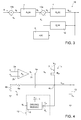
- a voltage regulator As illustrated in Figure 2 , a voltage regulator according to one embodiment of the present solution, designated as a whole by 10, has a configuration substantially similar to that of the voltage regulator 1 illustrated in Figure 1 , thus comprising (designated by the same reference numbers and not described again in detail): an error-amplifier stage 2; an output amplifier stage 4; and a divider stage 6.
- the voltage regulator 10 further comprises a compensation amplifier stage 12, having a compensation input 12a coupled to the output 4b of the output amplifier stage 4, and a compensation output 12b coupled to the input 4a of the same output amplifier stage 4 (and to the output 2c of the error-amplifier stage 2).
- the compensation amplifier stage 12 is further coupled to the supply source 3 for receiving the supply voltage V CC .
- the compensation amplifier stage 12 is configured to implement a pure derivator (i.e., with a transfer function substantially given by s ⁇ K F , without poles at least in the operating frequencies of the voltage regulator 10, and defined by a single zero) and an output impedance that is substantially infinite, for small signal, in the absence of current demand by the load; in other words, the presence of the derivator does not perturb the static biasing conditions of the system.
- a pure derivator i.e., with a transfer function substantially given by s ⁇ K F , without poles at least in the operating frequencies of the voltage regulator 10, and defined by a single zero
- an output impedance that is substantially infinite, for small signal, in the absence of current demand by the load; in other words, the presence of the derivator does not perturb the static biasing conditions of the system.
- the presence of the compensation amplifier stage 12 enables reduction of the value of capacitance C o required for the capacitor (here designated by 13) at output from the voltage regulator 10.
- the output capacitor 13, connected between the output 4b of the output amplifier stage 4 and the ground reference terminal, may thus be integrated in the same chip of the voltage regulator 10 and has a reduced value of capacitance C o , for example in the region of 100 pF.
- the compensation amplifier stage 12 introduces into the voltage regulator 10 a further control loop, faster than the external voltage control loop (implemented by the error-amplifier stage 2 on the basis of the feedback voltage V R ), which enables a fast reaction to the current demands at output.
- the compensation amplifier stage 12 allows to obtain a dominant pole at output from the error-amplifier stage 2, as desired, and also a reduced overshoot in the current I CC required from the supply source 3 and a high stability in regard to the load variations (i.e. it allows to obtain a large phase margin).
- FIG 3 shows the general block diagram of the voltage regulator 10 (for determination of the transfer function), where V s denotes the compensation voltage generated by the compensation amplifier stage 12, which is combined in a first adder block 15a with the amplified error voltage ⁇ E , at the output of the error-amplifier stage 2, to generate the biasing voltage V G for biasing the output stage 4, in particular a gate terminal of at least one corresponding output PMOS transistor (here not illustrated; for this reason, in what follows, the biasing voltage V G will be defined as "gate biasing voltage").
- V E is the error voltage, which is the result of the difference, in a second adder block 15b, between the reference voltage V i and the feedback voltage V R .
- a E (s) denotes the transfer function of the error-amplifier stage
- a O (s) denotes the transfer function of the output amplifier stage 4
- ⁇ F (s) denotes the transfer function of the compensation stage 12
- ⁇ (s) denotes the transfer function of the divider stage 6.
- T s ⁇ ⁇ A E 0 ⁇ A O 1 + s ⁇ pe ⁇ 1 + s ⁇ pt and has a dominant pole at low frequency ⁇ pt , separate from a pole at high frequency ⁇ pe ⁇ pt ⁇ ⁇ ⁇ pe
- the ratio between these two frequencies depends upon the sizing of the circuit, but normally may be assumed of the order of 100.
- ⁇ pt ⁇ po 1 + K F ⁇ A O ⁇ ⁇ po ⁇ ⁇ pt ⁇ 1 K F ⁇ A O
- the position of the aforesaid dominant pole ⁇ pt is thus determined by the value of the gain factor K F of the compensation amplifier stage 12.
- the dominant pole ⁇ pt has a very low frequency in such a way that control problems in the closed loop do not arise and a large phase margin is obtained. In particular, there is a reduced sensitivity of the properties of stability to capacitive variations of the load.
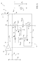
- the output amplifier stage 4 includes an output PMOS transistor, designated by M po , which is connected between the output 4b and the supply source 3 that supplies the supply voltage V CC and has its gate terminal connected to the input 4a (and to the output 2c of the error-amplifier stage 2).
- the compensation amplifier stage 12 in this case comprises: a coupling-capacitor element C F , which couples the output 4b of the output amplifier stage 4 to an internal node N1 of the compensation amplifier stage 12; and a driving module 16, coupled at its input to the internal node N1 and designed to generate the compensation voltage V S for driving the gate terminal of the output PMOS transistor M po .
- the capacitive coupling determined by the coupling-capacitor element C F causes the driving module 16 to have a high sensitivity, and a substantially immediate response to any variation of the output voltage V OUT , and consequent efficient driving of the output PMOS transistor M po . In this way, it is possible to obtain reduced voltage drops on the output 4b and reduced overshoots in the current consumption from the supply source (i.e., in the current I CC ).
- the driving module 16 is configured to generate a substantially instantaneous current path towards the input 4a of the output amplifier stage 4, for the gate capacitance of the output PMOS transistor M po , following upon a variation of the output voltage ⁇ V OUT , due to a load transient and the corresponding step of the load current I L at the output 4b of the output amplifier stage 4 (as represented by a load current generator 17, connected between the output 4b and the ground terminal).
- the above current path enabled upon the variation of output voltage ⁇ V OUT , generates a corresponding variation of the gate voltage for driving the output PMOS transistor M po .
- the aforesaid current path is determined by: a discharge PMOS transistor M p2 in source-follower configuration designed to enable driving of the output PMOS transistor M po (thus acting as a driver), which is connected between the input 4a of the output amplifier stage 4 (i.e., the gate terminal of the output PMOS transistor M po ) and an internal node N2, and has a respective gate terminal connected to an internal node N3, on which a voltage V F is present; and a biasing PMOS transistor M p3 , which is connected between the internal node N2 and the ground reference terminal and has its gate terminal that receives a p-biasing voltage V BIASP .
- the driving module 16 further comprises: a coupling PMOS transistor M p1 , which is diode-connected but is sufficiently resistive in such a way as to enable a considerable variation of voltage on the gate terminal of the discharge PMOS transistor M p2 when the latter is required to intervene in driving of the output PMOS transistor M po , having a first conduction terminal that is connected to the supply source 3 and receives the supply voltage V CC , and a second current-conduction terminal and its gate terminal that are both connected to the internal node N3; a first biasing NMOS transistor M n1 , which is connected between the second current-conduction terminal of the coupling PMOS transistor M p1 and the internal node N1, on which a voltage V F2 is present, and has a gate terminal that receives a n-biasing voltage V BIASN ; a second biasing NMOS transistor M n2 , connected between the internal node N2 and an internal node N4, on which a voltage V F1 is present, with its
- the demand at output for load current I L causes a voltage drop ⁇ V OUT , which, as a result of the capacitive coupling of the coupling-capacitor element C F , in turn causes a corresponding steplike decrease of the voltage V F2 on the internal node N1.
- the enabling PMOS transistor M p4 turns off, and the coupling PMOS transistor M p1 goes into a state of greater conduction, causing a decrease in voltage V F .
- the decrease in voltage V F causes the discharge PMOS transistor M p2 to go into a state of greater conduction, with setting-up of the discharge-current path through the same discharge PMOS transistor M p2 and the biasing PMOS transistor M p3 .
- the current I S that flows along the discharge-current path thus causes a decrease in the gate voltage V G on the gate terminal of the output PMOS transistor M po , in response to the voltage drop ⁇ V OUT , and an increase of the current that flows across the output PMOS transistor M po , in a way corresponding to the requirement of the load.
- the reaction of the circuit is very fast thanks to the role performed by the discharge PMOS transistor M p2 , which is able to conduct a high amount of current and to turn on the output PMOS transistor M P0 rapidly, notwithstanding the high capacitive load due to the size of the output PMOS transistor M P0 .
- Figures 7a and 7b show the plots of the magnitude and phase stability margins, with a value of capacitance of the output capacitor C o of 200 pF ( Figure 7a ) and 100 pF ( Figure 7b ) ; illustrated in each Figure 7a , 7b are the diagrams for different levels of load current I L , in particular 0, 0.5 mA, 1 mA, and 2 mA (the increase in current is indicated by the arrows in the same Figures 7a and 7b ).
- Figure 8 shows the overall equivalent diagram of the voltage regulator 10, with reference to the block diagram of Figure 3 , using the small-signal equivalent representations of the various circuit components.
- Figures 9a, 9b, and 9c-9d show individually the equivalent diagrams of the error-amplifier stage 2 ( Figure 9a ), of the output amplifier stage 4 ( Figure 9b ), and of the compensation amplifier stage 12 ( Figure 9c for calculation of the output impedance, and Figure 9d for calculation of the transfer function).
- the capacitance C G includes the capacitance due to the Miller effect of the output PMOS transistor M po (given by A O ⁇ C GD , where A O is the gain of the output amplifier stage 4 and C GD is the capacitance at the gate terminal of the output PMOS transistor M po ) ; and G me and r pe are the equivalent transconductance and the equivalent resistance, respectively, of the error-amplifier stage 2.
- the transfer function A E (s) may be modelled by a dominant pole ⁇ pe due to the capacitance C G and given by the expression (4), which is independent of the output parameters, in particular the capacitance of the output capacitor C o .
- Figure 9c regards, instead, calculation of the output impedance Z OF of the compensation amplifier stage 12; in Figure 9c : g mpf is the equivalent transconductance of the discharge PMOS transistor M p2 ; r pf is the equivalent resistance seen from the drain terminal of the discharge PMOS transistor M p2 (in these conditions, it is assumed that the biasing PMOS transistor M p3 is not in conduction and that the biasing NMOS transistor M n2 is working in the linear region); if is the current that flows in the biasing NMOS transistor M n2 ; g mf1 is the equivalent transconductance of the enabling PMOS transistor M p4 ; r f is the equivalent resistance of the coupling PMOS transistor M p1 ; and g mn is the equivalent transconductance of the biasing NMOS transistor M n1 .
- the output impedance Z OF is given by the following expression: I s ⁇ V s g mf 1 ⁇ r pf ⁇ r f ⁇ Z OF ⁇ g mf 1 ⁇ r pf ⁇ r f
- the compensation amplifier stage 12 of the voltage regulator 10 has a very high output impedance (for example, in the region of some megaohms), and a transfer function in which both of the poles are positioned at very high frequencies with respect to the operating frequency band, or range, of the voltage regulator 10 (for example, the operating frequency range is in the region of megahertz, and the poles are normally at a distance of at least one decade from said range).
- a derivator scheme is used with a very fast response, capable of driving the load (represented by the gate terminal of the large output PMOS transistor M po ) with an output stage implemented with a fast source-follower transistor, and with very low impedance when fast intervention is required.
- This characteristic is particularly advantageous in voltage regulation for supplying charge-pump circuits, the current demand of which is impulsive with sudden variations (in the region of a few nanoseconds) from zero to several milliamps.
- the compensation amplifier stage 12 operates as a pure derivator for the operating frequencies of interest and enables implementation of an effective separation of the poles and definition of a dominant pole, which is inedependent of the output parameters (in particular, the capacitance C o of the output capacitor 13).
- the solution described further enables a high stability to be obtained for all the possible conditions of load and values of load current I L ; in particular, the stability margin is greater than 60° in the worst case and greater than 85° in operating conditions of moderate load.
- the voltage regulator 10 implements an effective filtering of the current overshoots so that the waveform of the same current is smoothed and substantially without oscillations or spikes.
- this characteristic is particularly advantageous in the case of applications that require a high degree of security, or else reduced noise in the case of radiofrequency circuits.
- the area occupation is certainly reduced as compared to known solutions, for example less than 0.021 mm 2 , thanks to the use of an integrated output capacitor 13 of contained dimensions and of a low value, for example in the region of 100 pF.
- the voltage regulator 10 further presents: a PSRR of less of -15 dB for all the operating frequencies; a reduced drop in voltage ⁇ V, for example less than 100 mV during the transients; a lower static current consumption, for example less than 80 ⁇ A; and a fast response to input current steps with an amplitude comprised in a wide range of values, for example between 100 ⁇ A and 10 mA.
- the voltage regulator 10 may thus advantageously be used to supply a dedicated internal voltage source, for example in combination with a charge pump, this being a case where a low efficiency of the charge pump would in fact amplify static and dynamic current consumption.
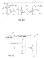
- Figure 10 is a schematic illustration of a nonvolatile memory device 20, in particular of a flash type (only the parts significant for the present discussion are illustrated in Figure 10 ).
- the nonvolatile memory device 20 comprises: an array of memory cells 22 (only one of which is shown by way of example); a decoder 24, designed to address the memory cells 22 for reading and programming operations; a DC/DC converter device including the voltage regulator 10; a charge pump 25, which supplies a boosted voltage V CP to the decoder 24 starting from the regulated output voltage V out supplied by the voltage regulator 10; and a controller 26, for example including a microprocessor or a microcontroller (or similar processing element), operatively coupled to the decoder 24.
Landscapes
- Engineering & Computer Science (AREA)
- Power Engineering (AREA)
- Physics & Mathematics (AREA)
- Electromagnetism (AREA)
- General Physics & Mathematics (AREA)
- Radar, Positioning & Navigation (AREA)
- Automation & Control Theory (AREA)
- Continuous-Control Power Sources That Use Transistors (AREA)
- Control Of Eletrric Generators (AREA)
- Electrical Discharge Machining, Electrochemical Machining, And Combined Machining (AREA)
Abstract
Description
- The present invention relates to a voltage regulator with improved electrical properties and to a corresponding control method.
- In a known manner, technological progress in the manufacturing of CMOS transistors, with ever smaller dimensions and thickness of the corresponding oxides, has led to a progressive reduction in the supply voltages used in the corresponding electronic circuits (in order not to cause damage thereto), for example down to values in the region of 1 V - 1.1 V.
- However, there is frequently the need to have available voltages different from the supply voltage, in particular of higher value; for this purpose, charge pumps are usually used, possibly combined to voltage regulators, in particular DC/DC converters, which have to meet stringent requirements from the standpoint of electrical performance in order not to jeopardize the general performance of the electronic circuits in which they are used.
- For instance, it is known that in nonvolatile memories, in particular of a flash type, operations of reading and programming, or modification, require high operating voltages for the terminals of the memory cells each time addressed, for example in the region of 5 V for the reading operations and 10 V for the programming operations.
- For generation of such operating voltages, charge-pump circuits are used, which, at their input, require regulated voltages of a value generally higher than the voltage supplied by the supply source, for example in the region of 1.4 V, for generation of which suitably configured voltage regulators are used.
- The electrical performance of these voltage regulators, for example in terms of static and dynamic consumption levels, output impedance, occupation of area, and stability margins, are particularly critical, for example on account of the inefficiency typical of the associated charge pumps.
- There are also applications entailing stringent safety requirements, for example in the case of the so-called "Secure MCUs", i.e., microprocessor units for secure applications, for example banking applications, computer security, payments, etc.
- In this case, further security requirements add to the aforesaid requirements relating to electrical performance, envisaging, for example, making not feasible the observation and understanding from outside, for example by monitoring the energy absorption from the electrical supply source, the operations performed by the circuit, such as reading or programming operations carried out in the memory.
-
Figure 1 shows a general block diagram of a voltage regulator, designated as a whole by 1, of a known type, which may be used, for example, for generation of the regulated input voltage required by a charge-pump circuit in a nonvolatile memory of a flash type. Thevoltage regulator 1 comprises: - an error-
amplifier stage 2, which is supplied by a supply source 3 (illustrated schematically) with a supply voltage VCC, of a low value (ICC is the current required of the supply source), and includes one or more operational-amplifier stages, in particular of an OTA (Operational Transconductance Amplifier) type;error amplifier stage 2 has afirst input 2a, receiving a reference voltage Vi, for example, from a band-gap generator (here not illustrated), asecond input 2b, designed to receive a feedback voltage VR for implementing a voltage control loop (as described more fully hereinafter), and anoutput 2c; - an
output amplifier stage 4, which is also supplied by the supply voltage VCC, and has aninput 4a connected to theoutput 2c of the error-amplifier stage 2, and anoutput 4b, which defines the output of thevoltage regulator 1 and supplies an output voltage VOUT, for example amplified by a desired amplification factor with respect to the reference voltage Vi; and - a
divider stage 6, which is connected to theoutput 4b of theoutput amplifier stage 4 and is designed to supply the feedback voltage VR, as a division of the output voltage VOUT, in order to implement feedback control of the value of the same output voltage VOUT; in the example illustrated, thedivider stage 6 is of a resistive type and thus comprises afirst division resistor 6a and asecond division resistor 6b, which are connected in series between theoutput 4b and a ground reference terminal and define a feedback node present on which is the feedback voltage VR (it is, however, evident that thedivider stage 6 could be of a capacitive type, in any case guaranteeing a low absorption of electrical current). - A storage capacitor 7 is further connected between the
output 4b of theoutput amplifier stage 4 and the ground reference terminal. This storage capacitor 7 has large dimensions and a high value of capacitance, for example in the region of nanofarads, and thus is generally not made with integrated technology, in particular is not made in the same chip as thevoltage regulator 1. - The
voltage regulator 1 thus implements a voltage control loop, in which the value of the output voltage VOUT is determined by the value of the reference voltage Vi and by the division factor implemented by thedivider stage 6 that generates the feedback voltage VR. - In particular, the high capacitance of the storage capacitor 7 is required to guarantee low drops in the output voltage ΔVOUT, define a dominant pole in the frequency response of the
voltage regulator 1, and rapidly meet the current demand during load transients. - Consequently, in this solution, the
voltage regulator 1 requires a high occupation of area for its implementation (in this regard, in a way not illustrated, also theoutput amplifier stage 4 requires use of PMOS transistors of large dimensions) in order to guarantee good characteristics of regulation as the load and the current demand vary. - The above solution is thus generally not suited to portable or mobile solutions, or in general applications in which the occupation of area represents an important design requirement.
- Different solutions have consequently been proposed, aimed at reducing area occupation, in particular ones envisaging elimination of the cumbersome storage capacitor 7 and its replacement with an output capacitor of lower capacitance, which may be integrated in the same chip in which the voltage regulator is provided.
- For instance, the document "External Capacitor-Less Low Drop-Out Regulator with 25dB Superior Power Supply Rejection in the 0.4 - 4MHz Range", C.J. Park, M. Onabajo, J. Silva-Martinez, JSSC, vol. 49, No. 2, February 2014, discusses possible voltage-regulator solutions aimed at eliminating the external storage capacitor, which has large dimensions.
- The solutions proposed in the above document require, however, complex circuit schemes for guaranteeing stability of the circuit and overcoming the absence of the dominant pole due to elimination of the storage capacitor; in particular, the circuit described envisages a pair of amplifiers with limited current capacity and high output impedance, which further introduce a long delay.
- The present Applicant has realized that in general existing solutions are not altogether satisfactory, especially in the case where the voltage regulator is used in applications with high security requirements. In fact, none of the known solutions enables an adequate control of the current consumption at output to be obtained, in particular as regards the so-called "overshoots", which may occur in response to sharp (steplike) variations of the current required by the load (and which, since they may be detected from outside, may jeopardize security of the system).
- On the other hand, in radiofrequency (RF) systems operating with reduced electromagnetic fields, it becomes increasingly important for the current responses of the peripherals to be free from peaks that might induce noise in the communication (signal-to-noise ratio).
- The need is thus certainly felt to provide an improved solution for a voltage regulator, which will make it possible to solve, or at least attenuate, the problems highlighted previously, and in particular that will have improved characteristics in reference to the current consumption and to the security provided, at the same time ensuring a reduced area occupation.
- The aim of the present invention is to meet the above need.
- According to the present invention, a voltage regulator, for example for a DC/DC converter, which may be used in a nonvolatile-memory device of a flash type, and a corresponding control method, are consequently provided as defined in the annexed claims.
- For a better understanding of the present invention, preferred embodiments thereof are now described, purely by way of non-limiting example and with reference to the attached drawings, wherein:
-
Figure 1 shows a general diagram of a voltage regulator, of a known type; -
Figure 2 shows a general diagram of a voltage regulator, according to one aspect of the present solution; -
Figure 3 shows an equivalent block diagram of the voltage regulator ofFigure 2 ; -
Figure 4 shows a more detailed diagram of the voltage regulator ofFigure 2 ; -
Figure 5 shows a possible circuit implementation of a compensation stage in the voltage regulator ofFigure 2 ; -
Figures 6 and 7a-7b show plots of electrical quantities in the voltage regulator ofFigure 2 ; -
Figure 8 is a schematic representation of the voltage regulator ofFigure 2 , for determination of the transfer function; -
Figures 9a-9d are schematic representations of blocks constituting the voltage regulator, for determination of the corresponding transfer function; and -
Figure 10 is a simplified block diagram of an electronic device, in particular a nonvolatile-memory device, in which the voltage regulator ofFigure 2 may be used. - As illustrated in
Figure 2 , a voltage regulator according to one embodiment of the present solution, designated as a whole by 10, has a configuration substantially similar to that of thevoltage regulator 1 illustrated inFigure 1 , thus comprising (designated by the same reference numbers and not described again in detail): an error-amplifier stage 2; anoutput amplifier stage 4; and adivider stage 6. - The
voltage regulator 10 further comprises acompensation amplifier stage 12, having acompensation input 12a coupled to theoutput 4b of theoutput amplifier stage 4, and acompensation output 12b coupled to theinput 4a of the same output amplifier stage 4 (and to theoutput 2c of the error-amplifier stage 2). - The
compensation amplifier stage 12 is further coupled to thesupply source 3 for receiving the supply voltage VCC. - According to an aspect of the present solution, the
compensation amplifier stage 12 is configured to implement a pure derivator (i.e., with a transfer function substantially given by s·KF, without poles at least in the operating frequencies of thevoltage regulator 10, and defined by a single zero) and an output impedance that is substantially infinite, for small signal, in the absence of current demand by the load; in other words, the presence of the derivator does not perturb the static biasing conditions of the system. - As described in detail hereinafter, the presence of the
compensation amplifier stage 12 enables reduction of the value of capacitance Co required for the capacitor (here designated by 13) at output from thevoltage regulator 10. In this case, theoutput capacitor 13, connected between theoutput 4b of theoutput amplifier stage 4 and the ground reference terminal, may thus be integrated in the same chip of thevoltage regulator 10 and has a reduced value of capacitance Co, for example in the region of 100 pF. - The
compensation amplifier stage 12 introduces into the voltage regulator 10 a further control loop, faster than the external voltage control loop (implemented by the error-amplifier stage 2 on the basis of the feedback voltage VR), which enables a fast reaction to the current demands at output. - In particular, the
compensation amplifier stage 12 allows to obtain a dominant pole at output from the error-amplifier stage 2, as desired, and also a reduced overshoot in the current ICC required from thesupply source 3 and a high stability in regard to the load variations (i.e. it allows to obtain a large phase margin). -
Figure 3 shows the general block diagram of the voltage regulator 10 (for determination of the transfer function), where Vs denotes the compensation voltage generated by thecompensation amplifier stage 12, which is combined in afirst adder block 15a with the amplified error voltage ṼE , at the output of the error-amplifier stage 2, to generate the biasing voltage VG for biasing theoutput stage 4, in particular a gate terminal of at least one corresponding output PMOS transistor (here not illustrated; for this reason, in what follows, the biasing voltage VG will be defined as "gate biasing voltage"). - In the same
Figure 3 , designated by VE is the error voltage, which is the result of the difference, in asecond adder block 15b, between the reference voltage Vi and the feedback voltage VR. - Furthermore, AE(s) denotes the transfer function of the error-amplifier stage, AO(s) denotes the transfer function of the
output amplifier stage 4, βF(s) denotes the transfer function of thecompensation stage 12, and α(s) denotes the transfer function of thedivider stage 6. - In particular, the following expressions apply:


- The open-loop transfer function of the
voltage regulator 10 is thus given by
and has a dominant pole at low frequency ωpt, separate from a pole at high frequency ωpe
- The ratio between these two frequencies depends upon the sizing of the circuit, but normally may be assumed of the order of 100.
- In particular, the following expression applies:

- The position of the aforesaid dominant pole ωpt is thus determined by the value of the gain factor KF of the
compensation amplifier stage 12. - It should be noted that the separation (or splitting) between the poles is obtained thanks to the presence of the pure derivator introduced in the further control loop. The solution described does not use Miller pole-splitting technique so as not to incur in the known problems regarding PSRR (Power-Supply Rejection Ratio) and RHZ (Right-Half-plane Zero).
- The dominant pole ωpt has a very low frequency in such a way that control problems in the closed loop do not arise and a large phase margin is obtained. In particular, there is a reduced sensitivity of the properties of stability to capacitive variations of the load.
- With reference to
Figure 4 , a description of a possible implementation of thecompensation amplifier stage 12, designed to implement the transfer function discussed previously, is presented. - In
Figure 4 , theoutput amplifier stage 4 includes an output PMOS transistor, designated by Mpo, which is connected between theoutput 4b and thesupply source 3 that supplies the supply voltage VCC and has its gate terminal connected to theinput 4a (and to theoutput 2c of the error-amplifier stage 2). - The
compensation amplifier stage 12 in this case comprises: a coupling-capacitor element CF, which couples theoutput 4b of theoutput amplifier stage 4 to an internal node N1 of thecompensation amplifier stage 12; and adriving module 16, coupled at its input to the internal node N1 and designed to generate the compensation voltage VS for driving the gate terminal of the output PMOS transistor Mpo. - The capacitive coupling determined by the coupling-capacitor element CF causes the
driving module 16 to have a high sensitivity, and a substantially immediate response to any variation of the output voltage VOUT, and consequent efficient driving of the output PMOS transistor Mpo. In this way, it is possible to obtain reduced voltage drops on theoutput 4b and reduced overshoots in the current consumption from the supply source (i.e., in the current ICC). - With reference to
Figure 5 , a possible circuit implementation of thedriving module 16 of thecompensation amplifier stage 12 is now described. - The driving
module 16 is configured to generate a substantially instantaneous current path towards theinput 4a of theoutput amplifier stage 4, for the gate capacitance of the output PMOS transistor Mpo, following upon a variation of the output voltage ΔVOUT, due to a load transient and the corresponding step of the load current IL at theoutput 4b of the output amplifier stage 4 (as represented by a loadcurrent generator 17, connected between theoutput 4b and the ground terminal). - The above current path, enabled upon the variation of output voltage ΔVOUT, generates a corresponding variation of the gate voltage for driving the output PMOS transistor Mpo.
- In detail, the aforesaid current path is determined by: a discharge PMOS transistor Mp2 in source-follower configuration designed to enable driving of the output PMOS transistor Mpo (thus acting as a driver), which is connected between the
input 4a of the output amplifier stage 4 (i.e., the gate terminal of the output PMOS transistor Mpo) and an internal node N2, and has a respective gate terminal connected to an internal node N3, on which a voltage VF is present; and a biasing PMOS transistor Mp3, which is connected between the internal node N2 and the ground reference terminal and has its gate terminal that receives a p-biasing voltage VBIASP. - The driving
module 16 further comprises: a coupling PMOS transistor Mp1, which is diode-connected but is sufficiently resistive in such a way as to enable a considerable variation of voltage on the gate terminal of the discharge PMOS transistor Mp2 when the latter is required to intervene in driving of the output PMOS transistor Mpo, having a first conduction terminal that is connected to thesupply source 3 and receives the supply voltage VCC, and a second current-conduction terminal and its gate terminal that are both connected to the internal node N3; a first biasing NMOS transistor Mn1, which is connected between the second current-conduction terminal of the coupling PMOS transistor Mp1 and the internal node N1, on which a voltage VF2 is present, and has a gate terminal that receives a n-biasing voltage VBIASN; a second biasing NMOS transistor Mn2, connected between the internal node N2 and an internal node N4, on which a voltage VF1 is present, with its gate terminal that receives the n-biasing voltage VBIASN; a biasing-current generator 18, which supplies a biasing current IBIAS to the internal node N4; and an enabling PMOS transistor Mp4, which is connected between the internal node N1 and the ground reference terminal and has its gate terminal connected to the internal node N4. - During operation, the demand at output for load current IL causes a voltage drop ΔVOUT, which, as a result of the capacitive coupling of the coupling-capacitor element CF, in turn causes a corresponding steplike decrease of the voltage VF2 on the internal node N1.
- On account of this variation of the voltage VF2, the enabling PMOS transistor Mp4 turns off, and the coupling PMOS transistor Mp1 goes into a state of greater conduction, causing a decrease in voltage VF. In turn, the decrease in voltage VF causes the discharge PMOS transistor Mp2 to go into a state of greater conduction, with setting-up of the discharge-current path through the same discharge PMOS transistor Mp2 and the biasing PMOS transistor Mp3.
- The current IS that flows along the discharge-current path thus causes a decrease in the gate voltage VG on the gate terminal of the output PMOS transistor Mpo, in response to the voltage drop ΔVOUT, and an increase of the current that flows across the output PMOS transistor Mpo, in a way corresponding to the requirement of the load.
- The reaction of the circuit is very fast thanks to the role performed by the discharge PMOS transistor Mp2, which is able to conduct a high amount of current and to turn on the output PMOS transistor MP0 rapidly, notwithstanding the high capacitive load due to the size of the output PMOS transistor MP0.
- Possible plots of the significant electrical quantities in the
driving module 16 are shown inFigure 6 , in response to steplike variations of the load current IL, highlighting the operation described in detail previously. - In particular, from an analysis of these plots, the following may be noted:
- the high stability and absence of oscillations on the gate voltage VG;
- the limited value of the overshoots in the current ICC required of the
supply source 3, which are at the most in the region of 10% with respect to the maximum value of the steps of the load current IL; and - the limited value of the voltage drop ΔVOUT, which in the example is just 100 mV (for a current step that goes from 0 to 3 mA in just 10 ns).
-
Figures 7a and7b show the plots of the magnitude and phase stability margins, with a value of capacitance of the output capacitor Co of 200 pF (Figure 7a ) and 100 pF (Figure 7b ) ; illustrated in eachFigure 7a ,7b are the diagrams for different levels of load current IL, in particular 0, 0.5 mA, 1 mA, and 2 mA (the increase in current is indicated by the arrows in the sameFigures 7a and7b ). - As may be noted, the stability properties are in general very good: using a value of capacitance of the output capacitor Co of 200 pF (
Figure 7a ), it is possible to obtain in fact a phase margin greater than 85° with a load current IL > 0.5 mA, and in any case greater than 63° in the worst case (load current IL = 0 mA); using, instead, a lower value of capacitance of the output capacitor Co, 100 pF (Figure 7b ), it is still possible to obtain a phase margin of 59° (in the worst case of a zero load current IL). - Tests and simulations conducted by the present Applicant have in any case highlighted a generally low sensitivity to variations of the capacitance Co of
output capacitor 13. -
Figure 8 shows the overall equivalent diagram of thevoltage regulator 10, with reference to the block diagram ofFigure 3 , using the small-signal equivalent representations of the various circuit components. For convenience of illustration,Figures 9a, 9b, and 9c-9d show individually the equivalent diagrams of the error-amplifier stage 2 (Figure 9a ), of the output amplifier stage 4 (Figure 9b ), and of the compensation amplifier stage 12 (Figure 9c for calculation of the output impedance, andFigure 9d for calculation of the transfer function). - Reference is first made to
Figure 9a , where: the capacitance CG includes the capacitance due to the Miller effect of the output PMOS transistor Mpo (given by AO·CGD, where AO is the gain of theoutput amplifier stage 4 and CGD is the capacitance at the gate terminal of the output PMOS transistor Mpo) ; and Gme and rpe are the equivalent transconductance and the equivalent resistance, respectively, of the error-amplifier stage 2. - It may be shown that the transfer function AE(s) of the error-
amplifier stage 2 is defined by the following expressions:



- In particular, the transfer function AE(s) may be modelled by a dominant pole ωpe due to the capacitance CG and given by the expression (4), which is independent of the output parameters, in particular the capacitance of the output capacitor Co.
- With reference to
Figure 9b , where α is the division ratio defined by theresistive divider 6, and gmpo is the equivalent transconductance of theoutput amplifier stage 4, the transfer function AO(s) of theoutput amplifier stage 4 is defined, instead, by the following expressions:


where RLT = R1 + R2 and may be in the region of 80 kΩ, and R1 and R2 are the resistances of thedivision resistors -
Figure 9c regards, instead, calculation of the output impedance ZOF of thecompensation amplifier stage 12; inFigure 9c : gmpf is the equivalent transconductance of the discharge PMOS transistor Mp2; rpf is the equivalent resistance seen from the drain terminal of the discharge PMOS transistor Mp2 (in these conditions, it is assumed that the biasing PMOS transistor Mp3 is not in conduction and that the biasing NMOS transistor Mn2 is working in the linear region); if is the current that flows in the biasing NMOS transistor Mn2; gmf1 is the equivalent transconductance of the enabling PMOS transistor Mp4; rf is the equivalent resistance of the coupling PMOS transistor Mp1; and gmn is the equivalent transconductance of the biasing NMOS transistor Mn1. - The output impedance ZOF is given by the following expression:

-
Figure 9d regards, instead, calculation of the transfer function of thecompensation amplifier stage 12, for which the following expressions apply:


- Consequently, the
compensation amplifier stage 12 of thevoltage regulator 10 has a very high output impedance (for example, in the region of some megaohms), and a transfer function in which both of the poles are positioned at very high frequencies with respect to the operating frequency band, or range, of the voltage regulator 10 (for example, the operating frequency range is in the region of megahertz, and the poles are normally at a distance of at least one decade from said range). - The
compensation amplifier stage 12 thus effectively performs a derivator function given that it is without poles for the operating frequencies of interest, and has just one zero; the transfer function may thus effectively be approximated as
- The advantages of the solution proposed emerge clearly from the foregoing description.
- In particular, for compensation a derivator scheme is used with a very fast response, capable of driving the load (represented by the gate terminal of the large output PMOS transistor Mpo) with an output stage implemented with a fast source-follower transistor, and with very low impedance when fast intervention is required. This characteristic is particularly advantageous in voltage regulation for supplying charge-pump circuits, the current demand of which is impulsive with sudden variations (in the region of a few nanoseconds) from zero to several milliamps.
- The
compensation amplifier stage 12 operates as a pure derivator for the operating frequencies of interest and enables implementation of an effective separation of the poles and definition of a dominant pole, which is inedependent of the output parameters (in particular, the capacitance Co of the output capacitor 13). - The solution described further enables a high stability to be obtained for all the possible conditions of load and values of load current IL; in particular, the stability margin is greater than 60° in the worst case and greater than 85° in operating conditions of moderate load.
- Furthermore, a reduced overshoot in the current consumption from the supply source is obtained, at the most in the region of 10% in any operating condition. In other words, the
voltage regulator 10 implements an effective filtering of the current overshoots so that the waveform of the same current is smoothed and substantially without oscillations or spikes. - As mentioned previously, this characteristic is particularly advantageous in the case of applications that require a high degree of security, or else reduced noise in the case of radiofrequency circuits.
- Furthermore, the area occupation is certainly reduced as compared to known solutions, for example less than 0.021 mm2, thanks to the use of an
integrated output capacitor 13 of contained dimensions and of a low value, for example in the region of 100 pF. - The
voltage regulator 10 further presents: a PSRR of less of -15 dB for all the operating frequencies; a reduced drop in voltage ΔV, for example less than 100 mV during the transients; a lower static current consumption, for example less than 80 µA; and a fast response to input current steps with an amplitude comprised in a wide range of values, for example between 100 µA and 10 mA. - The
voltage regulator 10 may thus advantageously be used to supply a dedicated internal voltage source, for example in combination with a charge pump, this being a case where a low efficiency of the charge pump would in fact amplify static and dynamic current consumption. - In this regard,
Figure 10 is a schematic illustration of anonvolatile memory device 20, in particular of a flash type (only the parts significant for the present discussion are illustrated inFigure 10 ). - The
nonvolatile memory device 20 comprises: an array of memory cells 22 (only one of which is shown by way of example); adecoder 24, designed to address thememory cells 22 for reading and programming operations; a DC/DC converter device including thevoltage regulator 10; acharge pump 25, which supplies a boosted voltage VCP to thedecoder 24 starting from the regulated output voltage Vout supplied by thevoltage regulator 10; and acontroller 26, for example including a microprocessor or a microcontroller (or similar processing element), operatively coupled to thedecoder 24. - Finally, it is clear that modifications and variations may be made to what has been described and illustrated herein, without thereby departing from the scope of the present invention, as defined in the annexed claims.
- In particular, it is emphasized once more that the solution described may find advantageous application in all the devices that envisage use of a voltage-regulator circuit, in which improvement of the electrical performance is required, in particular with reference to the characteristics of current consumption, area occupation and security.
Claims (15)
- A voltage-regulator device (10) comprising:an error-amplifier stage (2) having a first input (2a) and a second input (2b), which are designed to receive a reference voltage (Vi) and a feedback voltage (VR), respectively, and an output (2c);an output amplifier stage (4), which has an input (4a) coupled to the output (2c) of the error-amplifier stage (2) and is designed to supply at its output (4b) an output voltage (VOUT) related to the reference voltage (Vi) by an amplification factor (α);a feedback stage (6), which is coupled to the output (4b) of the output amplifier stage (4) and is designed to generate the feedback voltage (VR) as a function of the output voltage (VOUT) for implementing a first feedback loop; anda compensation stage (12), which is set between the output (4b) and the input (4a) of the output amplifier stage (4) and is configured to implement a second feedback loop, which is designed to cause, in response to a variation of said output voltage (VOUT), a corresponding variation of a biasing voltage (VG) for the input (4a) of the output amplifier stage,wherein the compensation stage (12) comprises: a coupling-capacitor element (CF), connected between the output (4b) of the output amplifier stage (4) and a first internal node (N1); and a driving module (16), which has an input connected to the first internal node (N1) and an output connected to the input (4a) of the output amplifier stage (4) and is configured to generate a compensation voltage (VS) for driving the output amplifier stage (4).
- The device according to claim 1, wherein the output amplifier stage (4) comprises: an output MOS transistor (Mpo), which is connected between said output (4b) and a terminal (13) that receives a supply voltage (VCC), and has a control terminal connected to said input (4a), said biasing voltage (VG) being a control voltage supplied to said control terminal; and wherein the compensation voltage (VS) is designed for driving the control terminal of the output MOS transistor (Mpo).
- The device according to claim 1 or 2, wherein the compensation stage (12) is configured to implement a derivator, having a frequency response with one or more poles outside an operating frequency band of said voltage regulator (10), and a single zero; and wherein the second feedback loop has a higher response speed than the first feedback loop.
- The device according to claim 3, having a frequency response with a dominant pole (ωpe) at the output (2c) of the error-amplifier stage (2), at a frequency much lower than said one or more poles in the frequency response of the compensation stage (12).
- The device according to any one of the preceding claims, wherein said driving module (16) is configured to enable, immediately in response to variation of said output voltage (VOUT), a current path (IS) towards the input (4a) of the output amplifier stage (4).
- The device according to claim 5, wherein said driving module (16) comprises a discharge transistor (Mp2) in voltage-follower configuration, connected to the input (4a) of the output amplifier stage (4) and configured to implement said current path (IS) and supply the compensation voltage (VS).
- The device according to claim 6, wherein said driving module (16) further comprises: an enabling transistor (Mp4), which has a conduction terminal connected to the first internal node (N1) and on which a control voltage (VF2) is present, having a variation corresponding to the output voltage (VOUT), and designed to enable said discharge transistor (Mp2) for defining said current path (IS) and thus determining extraction of current from the control terminal of an output MOS transistor (Mpo) of the output amplifier stage (4).
- The device according to claim 7, wherein said discharge transistor (Mp2) is connected between the input (4a) of the output amplifier stage (4) and a second internal node (N2) and has its control terminal connected to a third internal node (N3); wherein said driving module (16) further comprises: a coupling transistor (Mp1) diode-connected between a terminal (3) that receives a supply voltage (VCC) and the third internal node (N3); and a biasing transistor (Mp3), which is connected between the second internal node (N2) and a ground reference terminal and has a control terminal receiving a biasing voltage (VBIASP); said discharge transistor (Mp2) and biasing transistor (Mp3) designed to define said current path (Is).
- The device according to claim 8, wherein said driving module further comprises a first further biasing transistor (Mn1), which is connected between the third internal node (N3) and the first internal node (N1) and has a respective control terminal receiving a respective biasing voltage (VBIASN); and a second further biasing transistor (Mn2), which is connected between the second internal node (N2) and a control terminal of the enabling transistor (Mp4) and has a respective control terminal receiving the respective biasing voltage (VBIASN).
- The device according to any one of the preceding claims, wherein said feedback stage (6) comprises a divider, designed to generate said feedback voltage (VR) as a division of said output voltage (VOUT).
- An electronic circuit, comprising: the voltage-regulator device (10) according to any one of the preceding claims; and a charge-pump stage (25), which is connected to the output (4b) of said output amplifier stage (4) and is designed to generate a boosted voltage (VCP) starting from the output voltage (VOUT).
- A nonvolatile memory (20), comprising an array of memory cells (22) and the electronic circuit according to claim 11, designed to generate biasing voltages for the memory cells of said array of memory cells (22) starting from said boosted voltage (VCP).
- A method for controlling a voltage regulator (10) comprising:an error-amplifier stage (2) having a first input (2a) and a second input (2b), which are designed to receive a reference voltage (Vi) and a feedback voltage (VR), respectively, and an output (2c); andan output amplifier stage (4), which has an input (4a) coupled to the output (2c) of the error-amplifier stage (2) and is designed to supply at output (4b) an output voltage (VOUT) related to the reference voltage (Vi) by an amplification factor (α),comprising the steps of:implementing a first feedback loop by means of a feedback stage (6) coupled to the output (4b) of the output amplifier stage (4) to generate the feedback voltage (VR) as a function of the output voltage (VOUT); andimplementing a second feedback loop, by means of a compensation stage (12) set between the output (4b) and the input (4a) of the output amplifier stage (4), said second feedback loop being designed to cause, in response to a variation of said output voltage (VOUT), a corresponding variation of a biasing voltage (VG) at the input (4a) of the output amplifier stage (4),wherein implementing the second feedback loop comprises: connecting a coupling-capacitor element (CF) between the output (4b) of the output amplifier stage (4) and a first internal node (N1); and providing a driving module (16), having an input connected to the first internal node (N1) and an output connected to the input (4a) of the output amplifier stage (4), for generating a compensation voltage (VS) for said input (4a).
- The method according to claim 13, wherein implementing a second feedback loop comprises implementing a derivator, having a frequency response with one or more poles outside an operating frequency band of said voltage regulator (10) and a single zero; said second feedback loop having a higher speed of response than the first feedback loop.
- The method according to claim 14, wherein said voltage regulator (10) has a frequency response having a dominant pole (ωpe) at the output (2c) of said error-amplifier stage (2), at a frequency much lower than said one or more poles in the frequency response of said compensation stage (12).
Applications Claiming Priority (1)
| Application Number | Priority Date | Filing Date | Title |
|---|---|---|---|
| ITUB2015A001005A ITUB20151005A1 (en) | 2015-05-27 | 2015-05-27 | VOLTAGE REGULATOR WITH IMPROVED ELECTRICAL CHARACTERISTICS AND CORRESPONDING CONTROL METHOD |
Publications (3)
| Publication Number | Publication Date |
|---|---|
| EP3107209A2 true EP3107209A2 (en) | 2016-12-21 |
| EP3107209A3 EP3107209A3 (en) | 2017-04-05 |
| EP3107209B1 EP3107209B1 (en) | 2018-08-29 |
Family
ID=53765469
Family Applications (1)
| Application Number | Title | Priority Date | Filing Date |
|---|---|---|---|
| EP15200610.2A Active EP3107209B1 (en) | 2015-05-27 | 2015-12-16 | Voltage regulator with improved electrical properties and corresponding control method |
Country Status (3)
| Country | Link |
|---|---|
| US (2) | US9684324B2 (en) |
| EP (1) | EP3107209B1 (en) |
| IT (1) | ITUB20151005A1 (en) |
Cited By (1)
| Publication number | Priority date | Publication date | Assignee | Title |
|---|---|---|---|---|
| US10423178B1 (en) | 2018-10-12 | 2019-09-24 | Yangtze Memory Technologies Co., Ltd. | LDO regulator using NMOS transistor |
Families Citing this family (25)
| Publication number | Priority date | Publication date | Assignee | Title |
|---|---|---|---|---|
| ITUB20151005A1 (en) * | 2015-05-27 | 2016-11-27 | St Microelectronics Srl | VOLTAGE REGULATOR WITH IMPROVED ELECTRICAL CHARACTERISTICS AND CORRESPONDING CONTROL METHOD |
| CN104950974B (en) * | 2015-06-30 | 2017-05-31 | 华为技术有限公司 | Low pressure difference linear voltage regulator and the method and phaselocked loop that increase its stability |
| CN107526388B (en) * | 2016-06-22 | 2018-10-30 | 上海和辉光电有限公司 | Low pressure difference linear voltage regulator |
| US10078342B2 (en) * | 2016-06-24 | 2018-09-18 | International Business Machines Corporation | Low dropout voltage regulator with variable load compensation |
| US9946283B1 (en) * | 2016-10-18 | 2018-04-17 | Qualcomm Incorporated | Fast transient response low-dropout (LDO) regulator |
| US10033270B2 (en) * | 2016-10-26 | 2018-07-24 | International Business Machines Corporation | Dynamic voltage regulation |
| CN106788356B (en) * | 2016-12-13 | 2019-04-26 | 电子科技大学 | A Linear Regulator with Real-time Frequency Compensation |
| US10013010B1 (en) * | 2017-01-05 | 2018-07-03 | Qualcomm Incorporated | Voltage droop mitigation circuit for power supply network |
| US10903793B2 (en) * | 2017-06-30 | 2021-01-26 | Intel Corporation | Voltage regulators having regulated voltage output irrespective of input voltage |
| US10411599B1 (en) | 2018-03-28 | 2019-09-10 | Qualcomm Incorporated | Boost and LDO hybrid converter with dual-loop control |
| TWI666538B (en) * | 2018-04-24 | 2019-07-21 | 瑞昱半導體股份有限公司 | Voltage regulator and voltage regulating method |
| US10444780B1 (en) | 2018-09-20 | 2019-10-15 | Qualcomm Incorporated | Regulation/bypass automation for LDO with multiple supply voltages |
| US10591938B1 (en) | 2018-10-16 | 2020-03-17 | Qualcomm Incorporated | PMOS-output LDO with full spectrum PSR |
| US10545523B1 (en) | 2018-10-25 | 2020-01-28 | Qualcomm Incorporated | Adaptive gate-biased field effect transistor for low-dropout regulator |
| JP6793772B2 (en) | 2019-03-13 | 2020-12-02 | 華邦電子股▲ふん▼有限公司Winbond Electronics Corp. | Voltage generator |
| CN111766914B (en) * | 2019-04-01 | 2022-07-05 | 华邦电子股份有限公司 | voltage generator |
| CN110069092A (en) * | 2019-04-18 | 2019-07-30 | 上海华力微电子有限公司 | The current foldback circuit of LDO circuit device and LDO circuit |
| US11372436B2 (en) | 2019-10-14 | 2022-06-28 | Qualcomm Incorporated | Simultaneous low quiescent current and high performance LDO using single input stage and multiple output stages |
| CN110928358B (en) * | 2019-11-29 | 2021-11-09 | 芯原微电子(上海)股份有限公司 | Low dropout voltage regulating circuit |
| WO2021128199A1 (en) | 2019-12-26 | 2021-07-01 | 深圳市汇顶科技股份有限公司 | Regulator and chip |
| EP4185936A1 (en) | 2020-07-24 | 2023-05-31 | Qualcomm Incorporated | Charge pump based low dropout regulator |
| JP2022113967A (en) * | 2021-01-26 | 2022-08-05 | キオクシア株式会社 | semiconductor storage device |
| CN114299875B (en) * | 2021-12-24 | 2022-12-20 | 云谷(固安)科技有限公司 | Drive circuit, drive control unit and electronic equipment |
| US12498747B2 (en) * | 2022-08-05 | 2025-12-16 | Stmicroelectronics International N.V. | Short circuit fault protection for a regulator |
| JP2024049992A (en) * | 2022-09-29 | 2024-04-10 | エイブリック株式会社 | Voltage Regulator |
Family Cites Families (18)
| Publication number | Priority date | Publication date | Assignee | Title |
|---|---|---|---|---|
| US5563501A (en) | 1995-01-20 | 1996-10-08 | Linfinity Microelectronics | Low voltage dropout circuit with compensating capacitance circuitry |
| US5648718A (en) * | 1995-09-29 | 1997-07-15 | Sgs-Thomson Microelectronics, Inc. | Voltage regulator with load pole stabilization |
| US6246221B1 (en) * | 2000-09-20 | 2001-06-12 | Texas Instruments Incorporated | PMOS low drop-out voltage regulator using non-inverting variable gain stage |
| US6600299B2 (en) * | 2001-12-19 | 2003-07-29 | Texas Instruments Incorporated | Miller compensated NMOS low drop-out voltage regulator using variable gain stage |
| US6977490B1 (en) | 2002-12-23 | 2005-12-20 | Marvell International Ltd. | Compensation for low drop out voltage regulator |
| US7495422B2 (en) * | 2005-07-22 | 2009-02-24 | Hong Kong University Of Science And Technology | Area-efficient capacitor-free low-dropout regulator |
| TWI357543B (en) | 2008-03-24 | 2012-02-01 | Novatek Microelectronics Corp | Apparatus of dynamic feed-back control charge pump |
| CN101552552B (en) | 2008-04-02 | 2012-01-04 | 联咏科技股份有限公司 | Dynamic Feedback Regulated Charge Pump Device |
| US7733180B1 (en) | 2008-11-26 | 2010-06-08 | Texas Instruments Incorporated | Amplifier for driving external capacitive loads |
| TWI387359B (en) | 2009-01-21 | 2013-02-21 | Ite Tech Inc | Voltage generating apparatus for headphone |
| US8872492B2 (en) | 2010-04-29 | 2014-10-28 | Qualcomm Incorporated | On-chip low voltage capacitor-less low dropout regulator with Q-control |
| DE102010049009B4 (en) * | 2010-10-21 | 2013-01-24 | Texas Instruments Deutschland Gmbh | Electronic device and method for DC-DC conversion |
| US8169203B1 (en) | 2010-11-19 | 2012-05-01 | Nxp B.V. | Low dropout regulator |
| US8937464B2 (en) | 2011-07-15 | 2015-01-20 | Synopsys Inc. | High voltage generation system and method employing a charge pump and producing discrete voltage values |
| US9134743B2 (en) | 2012-04-30 | 2015-09-15 | Infineon Technologies Austria Ag | Low-dropout voltage regulator |
| CN103064455B (en) | 2012-12-07 | 2016-06-08 | 广州慧智微电子有限公司 | A kind of miller-compensated linear voltage regulator circuit of dynamic zero point based on zero-regulator resistor |
| CN103838290B (en) | 2014-03-17 | 2016-08-03 | 上海华虹宏力半导体制造有限公司 | Ldo circuit |
| ITUB20151005A1 (en) * | 2015-05-27 | 2016-11-27 | St Microelectronics Srl | VOLTAGE REGULATOR WITH IMPROVED ELECTRICAL CHARACTERISTICS AND CORRESPONDING CONTROL METHOD |
-
2015
- 2015-05-27 IT ITUB2015A001005A patent/ITUB20151005A1/en unknown
- 2015-12-15 US US14/969,103 patent/US9684324B2/en active Active
- 2015-12-16 EP EP15200610.2A patent/EP3107209B1/en active Active
-
2017
- 2017-05-16 US US15/596,895 patent/US9964976B2/en active Active
Non-Patent Citations (1)
| Title |
|---|
| C.J. PARK; M. ONABAJO; J. SILVA-MARTINEZ: "External Capacitor-Less Low Drop-Out Regulator with 25dB Superior Power Supply Rejection in the 0.4 - 4MHz Range", JSSC, vol. 49, no. 2, February 2014 (2014-02-01), XP011538050, DOI: doi:10.1109/JSSC.2013.2289897 |
Cited By (1)
| Publication number | Priority date | Publication date | Assignee | Title |
|---|---|---|---|---|
| US10423178B1 (en) | 2018-10-12 | 2019-09-24 | Yangtze Memory Technologies Co., Ltd. | LDO regulator using NMOS transistor |
Also Published As
| Publication number | Publication date |
|---|---|
| EP3107209A3 (en) | 2017-04-05 |
| EP3107209B1 (en) | 2018-08-29 |
| US20160349776A1 (en) | 2016-12-01 |
| US9684324B2 (en) | 2017-06-20 |
| US20170248981A1 (en) | 2017-08-31 |
| ITUB20151005A1 (en) | 2016-11-27 |
| US9964976B2 (en) | 2018-05-08 |
Similar Documents
| Publication | Publication Date | Title |
|---|---|---|
| EP3107209B1 (en) | Voltage regulator with improved electrical properties and corresponding control method | |
| US7397226B1 (en) | Low noise, low power, fast startup, and low drop-out voltage regulator | |
| EP4281840B1 (en) | Low-power voltage regulator with fast transient response | |
| US7368896B2 (en) | Voltage regulator with plural error amplifiers | |
| US7633280B2 (en) | Low drop voltage regulator with instant load regulation and method | |
| US20090128107A1 (en) | Low Dropout Voltage Regulator | |
| US9477244B2 (en) | Linear regulator with improved power supply ripple rejection | |
| JP5008472B2 (en) | Voltage regulator | |
| CN101604174B (en) | Voltage regulator | |
| EP1947544A1 (en) | Voltage regulator and method for voltage regulation | |
| CN110888484A (en) | Linear voltage regulator with low standby power consumption and high power supply rejection ratio | |
| US9785164B2 (en) | Power supply rejection for voltage regulators using a passive feed-forward network | |
| TWI639909B (en) | Voltage regulator | |
| US11249501B2 (en) | Voltage regulator | |
| EP1580637B1 (en) | Low drop-out DC voltage regulator | |
| US9367074B2 (en) | Voltage regulator capable of stabilizing an output voltage even when a power supply fluctuates | |
| CN108334149A (en) | A kind of high PSRR low differential voltage linear voltage stabilizer circuits of low quiescent current | |
| JP6457887B2 (en) | Voltage regulator | |
| KR20200123348A (en) | Voltage generator | |
| CN100456199C (en) | Alley Effect Elimination Circuit and Elimination Method, Differential Amplifier and Linear Regulator | |
| Mustafa et al. | Evolution of low drop out voltage regulator in CMOS technologies | |
| JP2017207902A (en) | Regulated power supply circuit | |
| US10534389B2 (en) | Device and method of compensation stabilization using Miller effect | |
| JP3819002B2 (en) | Semiconductor device | |
| KR20030002704A (en) | Regulator |
Legal Events
| Date | Code | Title | Description |
|---|---|---|---|
| PUAI | Public reference made under article 153(3) epc to a published international application that has entered the european phase |
Free format text: ORIGINAL CODE: 0009012 |
|
| AK | Designated contracting states |
Kind code of ref document: A2 Designated state(s): AL AT BE BG CH CY CZ DE DK EE ES FI FR GB GR HR HU IE IS IT LI LT LU LV MC MK MT NL NO PL PT RO RS SE SI SK SM TR |
|
| AX | Request for extension of the european patent |
Extension state: BA ME |
|
| PUAL | Search report despatched |
Free format text: ORIGINAL CODE: 0009013 |
|
| AK | Designated contracting states |
Kind code of ref document: A3 Designated state(s): AL AT BE BG CH CY CZ DE DK EE ES FI FR GB GR HR HU IE IS IT LI LT LU LV MC MK MT NL NO PL PT RO RS SE SI SK SM TR |
|
| AX | Request for extension of the european patent |
Extension state: BA ME |
|
| RIC1 | Information provided on ipc code assigned before grant |
Ipc: H03F 1/34 20060101AFI20170302BHEP Ipc: G05F 1/575 20060101ALI20170302BHEP Ipc: H03F 3/45 20060101ALI20170302BHEP Ipc: H03F 1/42 20060101ALI20170302BHEP Ipc: H02M 3/07 20060101ALI20170302BHEP Ipc: G05F 1/56 20060101ALI20170302BHEP |
|
| 17P | Request for examination filed |
Effective date: 20171005 |
|
| RBV | Designated contracting states (corrected) |
Designated state(s): AL AT BE BG CH CY CZ DE DK EE ES FI FR GB GR HR HU IE IS IT LI LT LU LV MC MK MT NL NO PL PT RO RS SE SI SK SM TR |
|
| GRAP | Despatch of communication of intention to grant a patent |
Free format text: ORIGINAL CODE: EPIDOSNIGR1 |
|
| INTG | Intention to grant announced |
Effective date: 20180316 |
|
| GRAS | Grant fee paid |
Free format text: ORIGINAL CODE: EPIDOSNIGR3 |
|
| GRAA | (expected) grant |
Free format text: ORIGINAL CODE: 0009210 |
|
| AK | Designated contracting states |
Kind code of ref document: B1 Designated state(s): AL AT BE BG CH CY CZ DE DK EE ES FI FR GB GR HR HU IE IS IT LI LT LU LV MC MK MT NL NO PL PT RO RS SE SI SK SM TR |
|
| REG | Reference to a national code |
Ref country code: GB Ref legal event code: FG4D |
|
| REG | Reference to a national code |
Ref country code: CH Ref legal event code: EP |
|
| REG | Reference to a national code |
Ref country code: AT Ref legal event code: REF Ref document number: 1036349 Country of ref document: AT Kind code of ref document: T Effective date: 20180915 |
|
| REG | Reference to a national code |
Ref country code: IE Ref legal event code: FG4D |
|
| REG | Reference to a national code |
Ref country code: DE Ref legal event code: R096 Ref document number: 602015015429 Country of ref document: DE |
|
| REG | Reference to a national code |
Ref country code: NL Ref legal event code: MP Effective date: 20180829 |
|
| REG | Reference to a national code |
Ref country code: LT Ref legal event code: MG4D |
|
| PG25 | Lapsed in a contracting state [announced via postgrant information from national office to epo] |
Ref country code: GR Free format text: LAPSE BECAUSE OF FAILURE TO SUBMIT A TRANSLATION OF THE DESCRIPTION OR TO PAY THE FEE WITHIN THE PRESCRIBED TIME-LIMIT Effective date: 20181130 Ref country code: FI Free format text: LAPSE BECAUSE OF FAILURE TO SUBMIT A TRANSLATION OF THE DESCRIPTION OR TO PAY THE FEE WITHIN THE PRESCRIBED TIME-LIMIT Effective date: 20180829 Ref country code: RS Free format text: LAPSE BECAUSE OF FAILURE TO SUBMIT A TRANSLATION OF THE DESCRIPTION OR TO PAY THE FEE WITHIN THE PRESCRIBED TIME-LIMIT Effective date: 20180829 Ref country code: IS Free format text: LAPSE BECAUSE OF FAILURE TO SUBMIT A TRANSLATION OF THE DESCRIPTION OR TO PAY THE FEE WITHIN THE PRESCRIBED TIME-LIMIT Effective date: 20181229 Ref country code: NO Free format text: LAPSE BECAUSE OF FAILURE TO SUBMIT A TRANSLATION OF THE DESCRIPTION OR TO PAY THE FEE WITHIN THE PRESCRIBED TIME-LIMIT Effective date: 20181129 Ref country code: NL Free format text: LAPSE BECAUSE OF FAILURE TO SUBMIT A TRANSLATION OF THE DESCRIPTION OR TO PAY THE FEE WITHIN THE PRESCRIBED TIME-LIMIT Effective date: 20180829 Ref country code: BG Free format text: LAPSE BECAUSE OF FAILURE TO SUBMIT A TRANSLATION OF THE DESCRIPTION OR TO PAY THE FEE WITHIN THE PRESCRIBED TIME-LIMIT Effective date: 20181129 Ref country code: SE Free format text: LAPSE BECAUSE OF FAILURE TO SUBMIT A TRANSLATION OF THE DESCRIPTION OR TO PAY THE FEE WITHIN THE PRESCRIBED TIME-LIMIT Effective date: 20180829 Ref country code: LT Free format text: LAPSE BECAUSE OF FAILURE TO SUBMIT A TRANSLATION OF THE DESCRIPTION OR TO PAY THE FEE WITHIN THE PRESCRIBED TIME-LIMIT Effective date: 20180829 |
|
| REG | Reference to a national code |
Ref country code: AT Ref legal event code: MK05 Ref document number: 1036349 Country of ref document: AT Kind code of ref document: T Effective date: 20180829 |
|
| PG25 | Lapsed in a contracting state [announced via postgrant information from national office to epo] |
Ref country code: HR Free format text: LAPSE BECAUSE OF FAILURE TO SUBMIT A TRANSLATION OF THE DESCRIPTION OR TO PAY THE FEE WITHIN THE PRESCRIBED TIME-LIMIT Effective date: 20180829 Ref country code: LV Free format text: LAPSE BECAUSE OF FAILURE TO SUBMIT A TRANSLATION OF THE DESCRIPTION OR TO PAY THE FEE WITHIN THE PRESCRIBED TIME-LIMIT Effective date: 20180829 Ref country code: AL Free format text: LAPSE BECAUSE OF FAILURE TO SUBMIT A TRANSLATION OF THE DESCRIPTION OR TO PAY THE FEE WITHIN THE PRESCRIBED TIME-LIMIT Effective date: 20180829 |
|
| PG25 | Lapsed in a contracting state [announced via postgrant information from national office to epo] |
Ref country code: ES Free format text: LAPSE BECAUSE OF FAILURE TO SUBMIT A TRANSLATION OF THE DESCRIPTION OR TO PAY THE FEE WITHIN THE PRESCRIBED TIME-LIMIT Effective date: 20180829 Ref country code: CZ Free format text: LAPSE BECAUSE OF FAILURE TO SUBMIT A TRANSLATION OF THE DESCRIPTION OR TO PAY THE FEE WITHIN THE PRESCRIBED TIME-LIMIT Effective date: 20180829 Ref country code: PL Free format text: LAPSE BECAUSE OF FAILURE TO SUBMIT A TRANSLATION OF THE DESCRIPTION OR TO PAY THE FEE WITHIN THE PRESCRIBED TIME-LIMIT Effective date: 20180829 Ref country code: RO Free format text: LAPSE BECAUSE OF FAILURE TO SUBMIT A TRANSLATION OF THE DESCRIPTION OR TO PAY THE FEE WITHIN THE PRESCRIBED TIME-LIMIT Effective date: 20180829 Ref country code: AT Free format text: LAPSE BECAUSE OF FAILURE TO SUBMIT A TRANSLATION OF THE DESCRIPTION OR TO PAY THE FEE WITHIN THE PRESCRIBED TIME-LIMIT Effective date: 20180829 Ref country code: EE Free format text: LAPSE BECAUSE OF FAILURE TO SUBMIT A TRANSLATION OF THE DESCRIPTION OR TO PAY THE FEE WITHIN THE PRESCRIBED TIME-LIMIT Effective date: 20180829 Ref country code: IT Free format text: LAPSE BECAUSE OF FAILURE TO SUBMIT A TRANSLATION OF THE DESCRIPTION OR TO PAY THE FEE WITHIN THE PRESCRIBED TIME-LIMIT Effective date: 20180829 |
|
| PG25 | Lapsed in a contracting state [announced via postgrant information from national office to epo] |
Ref country code: DK Free format text: LAPSE BECAUSE OF FAILURE TO SUBMIT A TRANSLATION OF THE DESCRIPTION OR TO PAY THE FEE WITHIN THE PRESCRIBED TIME-LIMIT Effective date: 20180829 Ref country code: SM Free format text: LAPSE BECAUSE OF FAILURE TO SUBMIT A TRANSLATION OF THE DESCRIPTION OR TO PAY THE FEE WITHIN THE PRESCRIBED TIME-LIMIT Effective date: 20180829 Ref country code: SK Free format text: LAPSE BECAUSE OF FAILURE TO SUBMIT A TRANSLATION OF THE DESCRIPTION OR TO PAY THE FEE WITHIN THE PRESCRIBED TIME-LIMIT Effective date: 20180829 |
|
| REG | Reference to a national code |
Ref country code: DE Ref legal event code: R097 Ref document number: 602015015429 Country of ref document: DE |
|
| PLBE | No opposition filed within time limit |
Free format text: ORIGINAL CODE: 0009261 |
|
| STAA | Information on the status of an ep patent application or granted ep patent |
Free format text: STATUS: NO OPPOSITION FILED WITHIN TIME LIMIT |
|
| REG | Reference to a national code |
Ref country code: CH Ref legal event code: PL |
|
| 26N | No opposition filed |
Effective date: 20190531 |
|
| PG25 | Lapsed in a contracting state [announced via postgrant information from national office to epo] |
Ref country code: LU Free format text: LAPSE BECAUSE OF NON-PAYMENT OF DUE FEES Effective date: 20181216 Ref country code: SI Free format text: LAPSE BECAUSE OF FAILURE TO SUBMIT A TRANSLATION OF THE DESCRIPTION OR TO PAY THE FEE WITHIN THE PRESCRIBED TIME-LIMIT Effective date: 20180829 Ref country code: MC Free format text: LAPSE BECAUSE OF FAILURE TO SUBMIT A TRANSLATION OF THE DESCRIPTION OR TO PAY THE FEE WITHIN THE PRESCRIBED TIME-LIMIT Effective date: 20180829 |
|
| REG | Reference to a national code |
Ref country code: IE Ref legal event code: MM4A |
|
| REG | Reference to a national code |
Ref country code: BE Ref legal event code: MM Effective date: 20181231 |
|
| PG25 | Lapsed in a contracting state [announced via postgrant information from national office to epo] |
Ref country code: FR Free format text: LAPSE BECAUSE OF NON-PAYMENT OF DUE FEES Effective date: 20181231 Ref country code: IE Free format text: LAPSE BECAUSE OF NON-PAYMENT OF DUE FEES Effective date: 20181216 |
|
| PG25 | Lapsed in a contracting state [announced via postgrant information from national office to epo] |
Ref country code: BE Free format text: LAPSE BECAUSE OF NON-PAYMENT OF DUE FEES Effective date: 20181231 |
|
| PG25 | Lapsed in a contracting state [announced via postgrant information from national office to epo] |
Ref country code: CH Free format text: LAPSE BECAUSE OF NON-PAYMENT OF DUE FEES Effective date: 20181231 Ref country code: LI Free format text: LAPSE BECAUSE OF NON-PAYMENT OF DUE FEES Effective date: 20181231 |
|
| PG25 | Lapsed in a contracting state [announced via postgrant information from national office to epo] |
Ref country code: MT Free format text: LAPSE BECAUSE OF NON-PAYMENT OF DUE FEES Effective date: 20181216 |
|
| PG25 | Lapsed in a contracting state [announced via postgrant information from national office to epo] |
Ref country code: TR Free format text: LAPSE BECAUSE OF FAILURE TO SUBMIT A TRANSLATION OF THE DESCRIPTION OR TO PAY THE FEE WITHIN THE PRESCRIBED TIME-LIMIT Effective date: 20180829 |
|
| PG25 | Lapsed in a contracting state [announced via postgrant information from national office to epo] |
Ref country code: PT Free format text: LAPSE BECAUSE OF FAILURE TO SUBMIT A TRANSLATION OF THE DESCRIPTION OR TO PAY THE FEE WITHIN THE PRESCRIBED TIME-LIMIT Effective date: 20180829 |
|
| PG25 | Lapsed in a contracting state [announced via postgrant information from national office to epo] |
Ref country code: HU Free format text: LAPSE BECAUSE OF FAILURE TO SUBMIT A TRANSLATION OF THE DESCRIPTION OR TO PAY THE FEE WITHIN THE PRESCRIBED TIME-LIMIT; INVALID AB INITIO Effective date: 20151216 Ref country code: CY Free format text: LAPSE BECAUSE OF FAILURE TO SUBMIT A TRANSLATION OF THE DESCRIPTION OR TO PAY THE FEE WITHIN THE PRESCRIBED TIME-LIMIT Effective date: 20180829 Ref country code: MK Free format text: LAPSE BECAUSE OF NON-PAYMENT OF DUE FEES Effective date: 20180829 |
|
| GBPC | Gb: european patent ceased through non-payment of renewal fee |
Effective date: 20191216 |
|
| PG25 | Lapsed in a contracting state [announced via postgrant information from national office to epo] |
Ref country code: GB Free format text: LAPSE BECAUSE OF NON-PAYMENT OF DUE FEES Effective date: 20191216 |
|
| PGFP | Annual fee paid to national office [announced via postgrant information from national office to epo] |
Ref country code: DE Payment date: 20251126 Year of fee payment: 11 |