EP3101730A1 - Antenna structure - Google Patents
Antenna structure Download PDFInfo
- Publication number
- EP3101730A1 EP3101730A1 EP15191180.7A EP15191180A EP3101730A1 EP 3101730 A1 EP3101730 A1 EP 3101730A1 EP 15191180 A EP15191180 A EP 15191180A EP 3101730 A1 EP3101730 A1 EP 3101730A1
- Authority
- EP
- European Patent Office
- Prior art keywords
- branch
- ground
- antenna structure
- radiation
- coupled
- Prior art date
- Legal status (The legal status is an assumption and is not a legal conclusion. Google has not performed a legal analysis and makes no representation as to the accuracy of the status listed.)
- Withdrawn
Links
- 230000005855 radiation Effects 0.000 claims abstract description 62
- 230000003071 parasitic effect Effects 0.000 claims description 10
- 238000010586 diagram Methods 0.000 description 16
- 229910052751 metal Inorganic materials 0.000 description 11
- 239000002184 metal Substances 0.000 description 11
- 238000004891 communication Methods 0.000 description 4
- 238000010295 mobile communication Methods 0.000 description 4
- XEEYBQQBJWHFJM-UHFFFAOYSA-N Iron Chemical compound [Fe] XEEYBQQBJWHFJM-UHFFFAOYSA-N 0.000 description 2
- 238000013461 design Methods 0.000 description 2
- 239000000758 substrate Substances 0.000 description 2
- RNFJDJUURJAICM-UHFFFAOYSA-N 2,2,4,4,6,6-hexaphenoxy-1,3,5-triaza-2$l^{5},4$l^{5},6$l^{5}-triphosphacyclohexa-1,3,5-triene Chemical compound N=1P(OC=2C=CC=CC=2)(OC=2C=CC=CC=2)=NP(OC=2C=CC=CC=2)(OC=2C=CC=CC=2)=NP=1(OC=1C=CC=CC=1)OC1=CC=CC=C1 RNFJDJUURJAICM-UHFFFAOYSA-N 0.000 description 1
- RYGMFSIKBFXOCR-UHFFFAOYSA-N Copper Chemical compound [Cu] RYGMFSIKBFXOCR-UHFFFAOYSA-N 0.000 description 1
- BQCADISMDOOEFD-UHFFFAOYSA-N Silver Chemical compound [Ag] BQCADISMDOOEFD-UHFFFAOYSA-N 0.000 description 1
- 229910045601 alloy Inorganic materials 0.000 description 1
- 239000000956 alloy Substances 0.000 description 1
- 229910052782 aluminium Inorganic materials 0.000 description 1
- XAGFODPZIPBFFR-UHFFFAOYSA-N aluminium Chemical compound [Al] XAGFODPZIPBFFR-UHFFFAOYSA-N 0.000 description 1
- 239000004020 conductor Substances 0.000 description 1
- 229910052802 copper Inorganic materials 0.000 description 1
- 239000010949 copper Substances 0.000 description 1
- 238000005516 engineering process Methods 0.000 description 1
- 239000003063 flame retardant Substances 0.000 description 1
- 229910052742 iron Inorganic materials 0.000 description 1
- 230000007774 longterm Effects 0.000 description 1
- 238000005259 measurement Methods 0.000 description 1
- 238000000034 method Methods 0.000 description 1
- 238000012986 modification Methods 0.000 description 1
- 230000004048 modification Effects 0.000 description 1
- 229910052709 silver Inorganic materials 0.000 description 1
- 239000004332 silver Substances 0.000 description 1
- 230000002123 temporal effect Effects 0.000 description 1
Images



Classifications
-
- H—ELECTRICITY
- H01—ELECTRIC ELEMENTS
- H01Q—ANTENNAS, i.e. RADIO AERIALS
- H01Q5/00—Arrangements for simultaneous operation of antennas on two or more different wavebands, e.g. dual-band or multi-band arrangements
- H01Q5/30—Arrangements for providing operation on different wavebands
- H01Q5/307—Individual or coupled radiating elements, each element being fed in an unspecified way
- H01Q5/342—Individual or coupled radiating elements, each element being fed in an unspecified way for different propagation modes
- H01Q5/357—Individual or coupled radiating elements, each element being fed in an unspecified way for different propagation modes using a single feed point
- H01Q5/364—Creating multiple current paths
- H01Q5/371—Branching current paths
-
- H—ELECTRICITY
- H01—ELECTRIC ELEMENTS
- H01Q—ANTENNAS, i.e. RADIO AERIALS
- H01Q1/00—Details of, or arrangements associated with, antennas
- H01Q1/12—Supports; Mounting means
- H01Q1/22—Supports; Mounting means by structural association with other equipment or articles
- H01Q1/24—Supports; Mounting means by structural association with other equipment or articles with receiving set
- H01Q1/241—Supports; Mounting means by structural association with other equipment or articles with receiving set used in mobile communications, e.g. GSM
- H01Q1/242—Supports; Mounting means by structural association with other equipment or articles with receiving set used in mobile communications, e.g. GSM specially adapted for hand-held use
- H01Q1/243—Supports; Mounting means by structural association with other equipment or articles with receiving set used in mobile communications, e.g. GSM specially adapted for hand-held use with built-in antennas
-
- H—ELECTRICITY
- H01—ELECTRIC ELEMENTS
- H01Q—ANTENNAS, i.e. RADIO AERIALS
- H01Q1/00—Details of, or arrangements associated with, antennas
- H01Q1/48—Earthing means; Earth screens; Counterpoises
-
- H—ELECTRICITY
- H01—ELECTRIC ELEMENTS
- H01Q—ANTENNAS, i.e. RADIO AERIALS
- H01Q5/00—Arrangements for simultaneous operation of antennas on two or more different wavebands, e.g. dual-band or multi-band arrangements
- H01Q5/40—Imbricated or interleaved structures; Combined or electromagnetically coupled arrangements, e.g. comprising two or more non-connected fed radiating elements
-
- H—ELECTRICITY
- H01—ELECTRIC ELEMENTS
- H01Q—ANTENNAS, i.e. RADIO AERIALS
- H01Q7/00—Loop antennas with a substantially uniform current distribution around the loop and having a directional radiation pattern in a plane perpendicular to the plane of the loop
Definitions
- the disclosure generally relates to an antenna structure, and more particularly, to a small-size antenna structure.
- mobile devices such as portable computers, mobile phones, multimedia players, and other hybrid functional portable electronic devices have become more common.
- mobile devices can usually perform wireless communication functions.
- Some devices cover a large wireless communication area; these include mobile phones using 2G, 3G, and LTE (Long Term Evolution) systems and using frequency bands of 700MHz, 850MHz, 900MHz, 1800MHz, 1900MHz, 2100MHz, 2300MHz, and 2500MHz.
- Some devices cover a small wireless communication area; these include mobile phones using Wi-Fi and Bluetooth systems and using frequency bands of 2.4GHz, 5.2GHz, and 5.8GHz.
- An antenna is indispensable in a mobile device supporting wireless communication.
- a mobile device since a mobile device often has limited interior space, there is not sufficient area for accommodating the required antenna element. Accordingly, it becomes a critical challenge for antenna designers to design a novel antenna with a small size and wideband characteristics.
- the invention is directed to an antenna structure including a ground element, a first radiation branch, a first ground branch, a second radiation branch, and a second ground branch.
- a first end of the first radiation branch is coupled to a signal source.
- a first end of the first ground branch is coupled to the ground element.
- a second end of the first ground branch is coupled to a second end of the first radiation branch.
- a first end of the second radiation branch is coupled to the second end of the first radiation branch.
- a first end of the second ground branch is coupled to the ground element.
- a second end of the second ground branch is coupled to a second end of the second radiation branch.
- the antenna structure includes a first loop structure and a second loop structure.
- the first loop structure is formed by the first radiation branch, the second radiation branch, the second ground branch, and the ground element.
- the second loop structure is formed by the first radiation branch, the first ground branch, and the ground element.
- a total length of the first loop structure is longer than a total length of the second loop structure.
- the first loop structure is excited to generate a first frequency band
- the second loop structure is excited to generate a second frequency band.
- the first frequency band is from about 2400MHz to about 2500MHz
- the second frequency band is from about 5150MHz to about 5850MHz.
- the first radiation branch has a U-shape
- each of the first ground branch, the second radiation branch, and the second ground branch has a straight-line shape
- the antenna structure further includes an extension branch.
- the extension branch is coupled to the second end of the second radiation branch and the second end of the second ground branch.
- the antenna structure further includes a parasitic branch.
- the parasitic branch is coupled to the ground element, and is disposed adjacent to the first radiation branch.
- the antenna structure further includes a feeding tuning branch.
- the feeding tuning branch is coupled to an initial portion of the first radiation branch, and is surrounded by the first radiation branch.
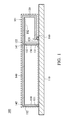
- FIG. 1 is a diagram of an antenna structure 100 according to an embodiment of the invention.
- the antenna structure 100 may be applied in a mobile device, such as a smartphone, a tablet computer, or a notebook computer.
- the antenna structure 100 includes a ground element 110, a first radiation branch 120, a first ground branch 130, a second radiation branch 140, and a second ground branch 150.
- the ground element 110 may be a ground metal plane of a mobile device.
- the first radiation branch 120, the first ground branch 130, the second radiation branch 140, and the second ground branch 150 may be made of conductive materials, such as copper, silver, aluminum, iron, or their alloys.
- the antenna structure 100 may be disposed on a dielectric substrate (not shown), such as a system circuit board or an FR4 (Flame Retardant 4) substrate.
- the first radiation branch 120 may substantially have a U-shape.
- the first radiation branch 120 has a first end 121 and a second end 122.
- the first end 121 of the first radiation branch 120 is coupled to a signal source 190.
- the signal source 190 may be an RF (Radio Frequency) module of a mobile device, and may be configured to excite the antenna structure 100.
- the first ground branch 130 may substantially have a straight-line shape, and may be substantially perpendicular to an edge of the ground element 110.
- the first ground branch 130 has a first end 131 and a second end 132.
- the first end 131 of the first ground branch 130 is coupled to the ground element 110.
- the second end 132 of the first ground branch 130 is coupled to the second end 122 of the first radiation branch 120.
- the second radiation branch 140 may substantially have a straight-line shape, and may be substantially parallel to the edge of the ground element 110.
- the second radiation branch 140 has a first end 141 and a second end 142.
- the first end 141 of the second radiation branch 140 is coupled to the second end 122 of the first radiation branch 120 and the second end 132 of the first ground branch 130.
- the second ground branch 150 may substantially have a straight-line shape, and may be substantially perpendicular to the edge of the ground element 110.
- the second ground branch 150 has a first end 151 and a second end 152.
- the first end 151 of the second ground branch 150 is coupled to the ground element 110.
- the second end 152 of the second ground branch 150 is coupled to the second end 142 of the second radiation branch 140.
- the antenna structure 100 includes a first loop structure 101 and a second loop structure 102.
- the first loop structure 101 is formed by the first radiation branch 120, the second radiation branch 140, the second ground branch 150, and a portion of the ground element 110.
- the second loop structure 102 is formed by the first radiation branch 120, the first ground branch 130, and another portion the ground element 110.
- the total length of the first loop structure 101 is longer than the total length of the second loop structure 102.
- the first frequency band is from about 2400MHz to about 2500MHz
- the second frequency band is from about 5150MHz to about 5850MHz.
- the antenna structure 100 of the invention is considered as a variation of a loop antenna.
- the difference from the conventional loop antenna is that the proposed antenna structure 100 has two combined loop structures respectively coupled to two different ground points on the ground element 110.
- One loop structure is excited to generate a low-frequency resonant mode, and another loop structure is excited to generate a high-frequency resonant mode. Since the two loop structures share portions of resonant paths (e.g., the resonant path of the first radiation branch 120), the total area of the antenna structure 100 can be reduced further.
- the proposed antenna structure 100 has a length of about 55mm and a width of about 11mm, and its antenna efficiency can achieve -4dBi in 2.4GHz/5GHz frequency bands. Therefore, the invention has the advantages of minimizing the antenna size, maintaining the antenna efficiency, and widening the antenna bandwidth, and it is suitable for application in a variety of small-size mobile communication devices.
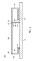
- FIG. 2 is a diagram of an antenna structure 200 according to an embodiment of the invention.
- FIG. 2 is similar to FIG. 1 .
- a second ground branch 250 of the antenna structure 200 has a meandering structure.
- the meandering structure may substantially have an N-shape or a W-shape.
- the design of the meandering second ground branch 250 can further reduce the total area of the antenna structure 200, and therefore the antenna structure 200 can be applied to small-size devices.
- Other features of the antenna structure 200 of FIG. 2 are similar to those of the antenna structure 100 of FIG. 1 . Accordingly, the two embodiments can achieve similar levels of performance.
- FIG. 3 is a diagram of an antenna structure 300 according to an embodiment of the invention.
- FIG. 3 is similar to FIG. 2 .
- the antenna structure 300 further includes an extension branch 360.
- the extension branch 360 may substantially have an L-shape.
- the extension branch 360 has a first end 361 and a second end 362.
- the first end 361 of the extension branch 360 is coupled to the second end 142 of the second radiation branch 140 and a second end 252 of the second ground branch 250.
- the second end 362 of the extension branch 360 is open.
- the extension branch 360 is configured to widen the bandwidth of the first frequency band (low-frequency band) of the antenna structure 300.
- Other features of the antenna structure 300 of FIG. 3 are similar to those of the antenna structure 200 of FIG. 2 . Accordingly, the two embodiments can achieve similar levels of performance.
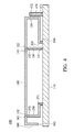
- FIG. 4 is a diagram of an antenna structure 400 according to an embodiment of the invention.
- FIG. 4 is similar to FIG. 3 .
- the antenna structure 400 further includes a parasitic branch 470.
- the parasitic branch 470 may substantially have a straight-line shape, and may be substantially perpendicular to the edge of the ground element 110.
- the parasitic branch 470 has a first end 471 and a second end 472.
- the first end 471 of the parasitic branch 470 is coupled to the ground element 110.
- the second end 472 of the parasitic branch 470 is open.
- the parasitic branch 470 is disposed adjacent to a bent portion of the first radiation branch 120, but is separate from the first radiation branch 120 completely.
- the parasitic branch 470 is configured to widen the bandwidth of the second frequency band (high-frequency band) of the antenna structure 400.
- Other features of the antenna structure 400 of FIG. 4 are similar to those of the antenna structure 300 of FIG. 3 . Accordingly, the two embodiments can achieve similar levels of performance.
- FIG. 5 is a diagram of an antenna structure 500 according to an embodiment of the invention.
- FIG. 5 is similar to FIG. 4 .
- the antenna structure 500 further includes a feeding tuning branch 580.
- the feeding tuning branch 580 may substantially have a rectangular shape, and may be substantially surrounded by the first radiation branch 120.
- the feeding tuning branch 580 has a first end 581 and a second end 582.
- the first end 581 of the feeding tuning branch 580 is coupled to an initial portion 123 of the first radiation branch 120.
- the second end 582 of the feeding tuning branch 580 is open.
- the feeding tuning branch 580 is configured to tune the feeding impedance matching of the antenna structure 500.
- Other features of the antenna structure 500 of FIG. 5 are similar to those of the antenna structure 400 of FIG. 4 . Accordingly, the two embodiments can achieve similar levels of performance.
- FIG. 6 is a diagram of VSWR (Voltage Standing Wave Ratio) of the antenna structure 500 according to an embodiment of the invention.
- the horizontal axis represents the operation frequency (MHz), and the vertical axis represents the VSWR.
- the antenna structure 500 covers at least the 2.4GHz low-frequency band (from about 2400MHz to about 2500MHz) and the 5GHz high-frequency band (from about 5150MHz to about 5850MHz). Therefore, the proposed antenna structure can support at least the dual-band operations of Wi-Fi and Bluetooth.
- the invention has sufficient antenna bandwidth and antenna efficiency, and it can meet the general standard of mobile communication.
- FIG. 7 is a diagram of an electronic device 700 according to an embodiment of the invention.
- the electronic device 700 may be a mobile communication device, such as a smartphone, a tablet computer, or a notebook computer.
- the electronic device 700 includes a metal back cover 710 and a display device 720.
- the antenna structure 100 (or 200 or 300 or 400 or 500) may be disposed on the top of the metal back cover 710.
- the ground element 110 of the antenna structure 100 may be coupled to the metal back cover 710, or may be coupled to a ground plane of a system circuit board (not shown).
- the ground plane of the system circuit board may be further coupled to the metal back cover 710.
- FIG. 8 is a diagram of an electronic device 800 according to an embodiment of the invention.
- FIG. 8 is similar to FIG. 7 .
- the difference between the two embodiments is that the relative relationship between the antenna structure 100 and the metal back cover 710 of FIG. 8 is slightly changed. That is, the antenna structure 100 is moved from the top to the left of the metal back cover 710. In alternative embodiments, the antenna structure 100 is moved to the bottom or the right of the metal back cover 710. In other embodiments, the antenna structure 100 is applied to an electronic device with a plastic back cover.
- the antenna structure of the invention is not limited to the configurations of FIGS. 1-8 .
- the invention may include any one or more features of any one or more embodiments of FIGS. 1-8 . In other words, not all of the features displayed in the figures should be implemented in the antenna structure of the invention.
Landscapes
- Physics & Mathematics (AREA)
- Electromagnetism (AREA)
- Engineering & Computer Science (AREA)
- Computer Networks & Wireless Communication (AREA)
- Support Of Aerials (AREA)
- Variable-Direction Aerials And Aerial Arrays (AREA)
Abstract
Description
- This Application claims priority of Taiwan Patent Application No.
104117909 filed on June 3, 2015 - The disclosure generally relates to an antenna structure, and more particularly, to a small-size antenna structure.
- With advancements in mobile communication technology, mobile devices such as portable computers, mobile phones, multimedia players, and other hybrid functional portable electronic devices have become more common. To satisfy user demand, mobile devices can usually perform wireless communication functions. Some devices cover a large wireless communication area; these include mobile phones using 2G, 3G, and LTE (Long Term Evolution) systems and using frequency bands of 700MHz, 850MHz, 900MHz, 1800MHz, 1900MHz, 2100MHz, 2300MHz, and 2500MHz. Some devices cover a small wireless communication area; these include mobile phones using Wi-Fi and Bluetooth systems and using frequency bands of 2.4GHz, 5.2GHz, and 5.8GHz.
- An antenna is indispensable in a mobile device supporting wireless communication. However, since a mobile device often has limited interior space, there is not sufficient area for accommodating the required antenna element. Accordingly, it becomes a critical challenge for antenna designers to design a novel antenna with a small size and wideband characteristics.
- In a preferred embodiment, the invention is directed to an antenna structure including a ground element, a first radiation branch, a first ground branch, a second radiation branch, and a second ground branch. A first end of the first radiation branch is coupled to a signal source. A first end of the first ground branch is coupled to the ground element. A second end of the first ground branch is coupled to a second end of the first radiation branch. A first end of the second radiation branch is coupled to the second end of the first radiation branch. A first end of the second ground branch is coupled to the ground element. A second end of the second ground branch is coupled to a second end of the second radiation branch.
- In some embodiments, the antenna structure includes a first loop structure and a second loop structure.
- In some embodiments, the first loop structure is formed by the first radiation branch, the second radiation branch, the second ground branch, and the ground element.
- In some embodiments, the second loop structure is formed by the first radiation branch, the first ground branch, and the ground element.
- In some embodiments, a total length of the first loop structure is longer than a total length of the second loop structure.
- In some embodiments, the first loop structure is excited to generate a first frequency band, and the second loop structure is excited to generate a second frequency band. The first frequency band is from about 2400MHz to about 2500MHz, and the second frequency band is from about 5150MHz to about 5850MHz.
- In some embodiments, the first radiation branch has a U-shape, and each of the first ground branch, the second radiation branch, and the second ground branch has a straight-line shape.
- In some embodiments, the antenna structure further includes an extension branch. The extension branch is coupled to the second end of the second radiation branch and the second end of the second ground branch.
- In some embodiments, the antenna structure further includes a parasitic branch. The parasitic branch is coupled to the ground element, and is disposed adjacent to the first radiation branch.
- In some embodiments, the antenna structure further includes a feeding tuning branch. The feeding tuning branch is coupled to an initial portion of the first radiation branch, and is surrounded by the first radiation branch.
- The invention can be more fully understood by reading the subsequent detailed description and examples with references made to the accompanying drawings, wherein:
-
FIG. 1 is a diagram of an antenna structure according to an embodiment of the invention; -
FIG. 2 is a diagram of an antenna structure according to an embodiment of the invention; -
FIG. 3 is a diagram of an antenna structure according to an embodiment of the invention; -
FIG. 4 is a diagram of an antenna structure according to an embodiment of the invention; -
FIG. 5 is a diagram of an antenna structure according to an embodiment of the invention; -
FIG. 6 is a diagram of VSWR (Voltage Standing Wave Ratio) of an antenna structure according to an embodiment of the invention; -
FIG. 7 is a diagram of an electronic device according to an embodiment of the invention; and -
FIG. 8 is a diagram of an electronic device according to an embodiment of the invention. - In order to illustrate the foregoing and other purposes, features and advantages of the invention, the embodiments and figures of the invention will be described in detail as follows.
-
FIG. 1 is a diagram of anantenna structure 100 according to an embodiment of the invention. Theantenna structure 100 may be applied in a mobile device, such as a smartphone, a tablet computer, or a notebook computer. As shown inFIG. 1 , theantenna structure 100 includes aground element 110, afirst radiation branch 120, afirst ground branch 130, asecond radiation branch 140, and asecond ground branch 150. Theground element 110 may be a ground metal plane of a mobile device. Thefirst radiation branch 120, thefirst ground branch 130, thesecond radiation branch 140, and thesecond ground branch 150 may be made of conductive materials, such as copper, silver, aluminum, iron, or their alloys. Theantenna structure 100 may be disposed on a dielectric substrate (not shown), such as a system circuit board or an FR4 (Flame Retardant 4) substrate. - The
first radiation branch 120 may substantially have a U-shape. Thefirst radiation branch 120 has afirst end 121 and asecond end 122. Thefirst end 121 of thefirst radiation branch 120 is coupled to asignal source 190. Thesignal source 190 may be an RF (Radio Frequency) module of a mobile device, and may be configured to excite theantenna structure 100. Thefirst ground branch 130 may substantially have a straight-line shape, and may be substantially perpendicular to an edge of theground element 110. Thefirst ground branch 130 has afirst end 131 and asecond end 132. Thefirst end 131 of thefirst ground branch 130 is coupled to theground element 110. Thesecond end 132 of thefirst ground branch 130 is coupled to thesecond end 122 of thefirst radiation branch 120. Thesecond radiation branch 140 may substantially have a straight-line shape, and may be substantially parallel to the edge of theground element 110. Thesecond radiation branch 140 has afirst end 141 and asecond end 142. Thefirst end 141 of thesecond radiation branch 140 is coupled to thesecond end 122 of thefirst radiation branch 120 and thesecond end 132 of thefirst ground branch 130. Thesecond ground branch 150 may substantially have a straight-line shape, and may be substantially perpendicular to the edge of theground element 110. Thesecond ground branch 150 has afirst end 151 and asecond end 152. Thefirst end 151 of thesecond ground branch 150 is coupled to theground element 110. Thesecond end 152 of thesecond ground branch 150 is coupled to thesecond end 142 of thesecond radiation branch 140. - As to the antenna theory, the
antenna structure 100 includes afirst loop structure 101 and asecond loop structure 102. Thefirst loop structure 101 is formed by thefirst radiation branch 120, thesecond radiation branch 140, thesecond ground branch 150, and a portion of theground element 110. Thesecond loop structure 102 is formed by thefirst radiation branch 120, thefirst ground branch 130, and another portion theground element 110. The total length of thefirst loop structure 101 is longer than the total length of thesecond loop structure 102. When theantenna structure 100 is excited, thefirst loop structure 101 is excited to generate a first frequency band, and thesecond loop structure 102 is excited to generate a second frequency band. The first frequency band is from about 2400MHz to about 2500MHz, and the second frequency band is from about 5150MHz to about 5850MHz. - To be brief, the
antenna structure 100 of the invention is considered as a variation of a loop antenna. The difference from the conventional loop antenna is that the proposedantenna structure 100 has two combined loop structures respectively coupled to two different ground points on theground element 110. One loop structure is excited to generate a low-frequency resonant mode, and another loop structure is excited to generate a high-frequency resonant mode. Since the two loop structures share portions of resonant paths (e.g., the resonant path of the first radiation branch 120), the total area of theantenna structure 100 can be reduced further. According to practical measurements, the proposedantenna structure 100 has a length of about 55mm and a width of about 11mm, and its antenna efficiency can achieve -4dBi in 2.4GHz/5GHz frequency bands. Therefore, the invention has the advantages of minimizing the antenna size, maintaining the antenna efficiency, and widening the antenna bandwidth, and it is suitable for application in a variety of small-size mobile communication devices. -
FIG. 2 is a diagram of anantenna structure 200 according to an embodiment of the invention.FIG. 2 is similar toFIG. 1 . In the embodiment ofFIG. 2 , asecond ground branch 250 of theantenna structure 200 has a meandering structure. The meandering structure may substantially have an N-shape or a W-shape. The design of the meanderingsecond ground branch 250 can further reduce the total area of theantenna structure 200, and therefore theantenna structure 200 can be applied to small-size devices. Other features of theantenna structure 200 ofFIG. 2 are similar to those of theantenna structure 100 ofFIG. 1 . Accordingly, the two embodiments can achieve similar levels of performance. -
FIG. 3 is a diagram of anantenna structure 300 according to an embodiment of the invention.FIG. 3 is similar toFIG. 2 . In the embodiment ofFIG. 3 , theantenna structure 300 further includes anextension branch 360. Theextension branch 360 may substantially have an L-shape. Theextension branch 360 has afirst end 361 and asecond end 362. Thefirst end 361 of theextension branch 360 is coupled to thesecond end 142 of thesecond radiation branch 140 and asecond end 252 of thesecond ground branch 250. Thesecond end 362 of theextension branch 360 is open. Theextension branch 360 is configured to widen the bandwidth of the first frequency band (low-frequency band) of theantenna structure 300. Other features of theantenna structure 300 ofFIG. 3 are similar to those of theantenna structure 200 ofFIG. 2 . Accordingly, the two embodiments can achieve similar levels of performance. -
FIG. 4 is a diagram of anantenna structure 400 according to an embodiment of the invention.FIG. 4 is similar toFIG. 3 . In the embodiment ofFIG. 4 , theantenna structure 400 further includes aparasitic branch 470. Theparasitic branch 470 may substantially have a straight-line shape, and may be substantially perpendicular to the edge of theground element 110. Theparasitic branch 470 has afirst end 471 and asecond end 472. Thefirst end 471 of theparasitic branch 470 is coupled to theground element 110. Thesecond end 472 of theparasitic branch 470 is open. Theparasitic branch 470 is disposed adjacent to a bent portion of thefirst radiation branch 120, but is separate from thefirst radiation branch 120 completely. Theparasitic branch 470 is configured to widen the bandwidth of the second frequency band (high-frequency band) of theantenna structure 400. Other features of theantenna structure 400 ofFIG. 4 are similar to those of theantenna structure 300 ofFIG. 3 . Accordingly, the two embodiments can achieve similar levels of performance. -
FIG. 5 is a diagram of anantenna structure 500 according to an embodiment of the invention.FIG. 5 is similar toFIG. 4 . In the embodiment ofFIG. 5 , theantenna structure 500 further includes afeeding tuning branch 580. Thefeeding tuning branch 580 may substantially have a rectangular shape, and may be substantially surrounded by thefirst radiation branch 120. Thefeeding tuning branch 580 has afirst end 581 and asecond end 582. Thefirst end 581 of thefeeding tuning branch 580 is coupled to aninitial portion 123 of thefirst radiation branch 120. Thesecond end 582 of thefeeding tuning branch 580 is open. Thefeeding tuning branch 580 is configured to tune the feeding impedance matching of theantenna structure 500. Other features of theantenna structure 500 ofFIG. 5 are similar to those of theantenna structure 400 ofFIG. 4 . Accordingly, the two embodiments can achieve similar levels of performance. -
FIG. 6 is a diagram of VSWR (Voltage Standing Wave Ratio) of theantenna structure 500 according to an embodiment of the invention. The horizontal axis represents the operation frequency (MHz), and the vertical axis represents the VSWR. According to the criterion of VSWR being equal to 4, theantenna structure 500 covers at least the 2.4GHz low-frequency band (from about 2400MHz to about 2500MHz) and the 5GHz high-frequency band (from about 5150MHz to about 5850MHz). Therefore, the proposed antenna structure can support at least the dual-band operations of Wi-Fi and Bluetooth. The invention has sufficient antenna bandwidth and antenna efficiency, and it can meet the general standard of mobile communication. - The antenna structure of the invention can be applied to an electronic device with a metal back cover, but it is not limited thereto.
FIG. 7 is a diagram of anelectronic device 700 according to an embodiment of the invention. Theelectronic device 700 may be a mobile communication device, such as a smartphone, a tablet computer, or a notebook computer. In the embodiment ofFIG. 7 , theelectronic device 700 includes ametal back cover 710 and adisplay device 720. The antenna structure 100 (or 200 or 300 or 400 or 500) may be disposed on the top of the metal backcover 710. Theground element 110 of theantenna structure 100 may be coupled to the metal backcover 710, or may be coupled to a ground plane of a system circuit board (not shown). The ground plane of the system circuit board may be further coupled to the metal backcover 710. The shortest spacing between theantenna structure 100 and the metal backcover 710 may be about 4.5mm. When the aforementioned spacing increases, the radiation performance of theantenna structure 100 is improved further. The vertical projection of theantenna structure 100 is inside the metal backcover 710. However, the vertical projection of theantenna structure 100 does not overlap with any portion of thedisplay device 720.FIG. 8 is a diagram of anelectronic device 800 according to an embodiment of the invention.FIG. 8 is similar toFIG. 7 . The difference between the two embodiments is that the relative relationship between theantenna structure 100 and the metal backcover 710 ofFIG. 8 is slightly changed. That is, theantenna structure 100 is moved from the top to the left of the metal backcover 710. In alternative embodiments, theantenna structure 100 is moved to the bottom or the right of the metal backcover 710. In other embodiments, theantenna structure 100 is applied to an electronic device with a plastic back cover. - Note that the above element sizes, element shapes, and frequency ranges are not limitations of the invention. An antenna designer can fine-tune these settings or values according to different requirements. It should be understood that the antenna structure of the invention is not limited to the configurations of
FIGS. 1-8 . The invention may include any one or more features of any one or more embodiments ofFIGS. 1-8 . In other words, not all of the features displayed in the figures should be implemented in the antenna structure of the invention. - Use of ordinal terms such as "first", "second", "third", etc., in the claims to modify a claim element does not by itself connote any priority, precedence, or order of one claim element over another or the temporal order in which acts of a method are performed, but are used merely as labels to distinguish one claim element having a certain name from another element having the same name (but for use of the ordinal term) to distinguish the claim elements.
- It will be apparent to those skilled in the art that various modifications and variations can be made in the invention. It is intended that the standard and examples be considered as exemplary only, with a true scope of the disclosed embodiments being indicated by the following claims and their equivalents.
Claims (10)
- An antenna structure, comprising:a ground element;a first radiation branch, having a first end and a second end, wherein the first end of the first radiation branch is coupled to a signal source;a first ground branch, having a first end and a second end, wherein the first end of the first ground branch is coupled to the ground element, and the second end of the first ground branch is coupled to the second end of the first radiation branch;a second radiation branch, having a first end and a second end, wherein the first end of the second radiation branch is coupled to the second end of the first radiation branch; anda second ground branch, having a first end and a second end, wherein the first end of the second ground branch is coupled to the ground element, and the second end of the second ground branch is coupled to the second end of the second radiation branch.
- The antenna structure as claimed in claim 1, wherein the antenna structure comprises a first loop structure and a second loop structure.
- The antenna structure as claimed in claim 2, wherein the first loop structure is formed by the first radiation branch, the second radiation branch, the second ground branch, and the ground element.
- The antenna structure as claimed in claim 2, wherein the second loop structure is formed by the first radiation branch, the first ground branch, and the ground element.
- The antenna structure as claimed in claim 2, wherein a total length of the first loop structure is longer than a total length of the second loop structure.
- The antenna structure as claimed in claim 2, wherein the first loop structure is excited to generate a first frequency band, the second loop structure is excited to generate a second frequency band, the first frequency band is from about 2400MHz to about 2500MHz, and the second frequency band is from about 5150MHz to about 5850MHz.
- The antenna structure as claimed in claim 1, wherein the first radiation branch has a U-shape, and each of the first ground branch, the second radiation branch, and the second ground branch has a straight-line shape.
- The antenna structure as claimed in claim 1, further comprising:an extension branch, coupled to the second end of the second radiation branch and the second end of the second ground branch.
- The antenna structure as claimed in claim 1, further comprising:a parasitic branch, coupled to the ground element, and disposed adjacent to the first radiation branch.
- The antenna structure as claimed in claim 1, further comprising:a feeding tuning branch, coupled to an initial portion of the first radiation branch, and surrounded by the first radiation branch.
Applications Claiming Priority (1)
| Application Number | Priority Date | Filing Date | Title |
|---|---|---|---|
| TW104117909A TWI558001B (en) | 2015-06-03 | 2015-06-03 | Antenna structure |
Publications (1)
| Publication Number | Publication Date |
|---|---|
| EP3101730A1 true EP3101730A1 (en) | 2016-12-07 |
Family
ID=54360122
Family Applications (1)
| Application Number | Title | Priority Date | Filing Date |
|---|---|---|---|
| EP15191180.7A Withdrawn EP3101730A1 (en) | 2015-06-03 | 2015-10-23 | Antenna structure |
Country Status (3)
| Country | Link |
|---|---|
| US (1) | US9761943B2 (en) |
| EP (1) | EP3101730A1 (en) |
| TW (1) | TWI558001B (en) |
Families Citing this family (3)
| Publication number | Priority date | Publication date | Assignee | Title |
|---|---|---|---|---|
| CN107967026B (en) * | 2017-11-23 | 2019-10-25 | Oppo广东移动通信有限公司 | Antenna assembly, terminal equipment and method for improving antenna radiation performance |
| WO2019183798A1 (en) * | 2018-03-27 | 2019-10-03 | 华为技术有限公司 | Antenna |
| CN115425403B (en) * | 2022-09-21 | 2025-08-26 | 歌尔科技有限公司 | Dual-band antenna and electronic equipment |
Citations (2)
| Publication number | Priority date | Publication date | Assignee | Title |
|---|---|---|---|---|
| US20060097918A1 (en) * | 2002-11-18 | 2006-05-11 | Tadashi Oshiyama | Antenna for a plurality of bands |
| EP2048739A1 (en) * | 2006-07-28 | 2009-04-15 | Murata Manufacturing Co. Ltd. | Antenna device and radio communication device |
Family Cites Families (11)
| Publication number | Priority date | Publication date | Assignee | Title |
|---|---|---|---|---|
| TW545712U (en) * | 2002-11-08 | 2003-08-01 | Hon Hai Prec Ind Co Ltd | Multi-band antenna |
| US7298339B1 (en) * | 2006-06-27 | 2007-11-20 | Nokia Corporation | Multiband multimode compact antenna system |
| TW200924291A (en) * | 2007-11-16 | 2009-06-01 | Advanced Connectek Inc | Multi-band antenna |
| TWI355777B (en) * | 2008-01-15 | 2012-01-01 | Wistron Neweb Corp | Antenna structure |
| TWI425709B (en) * | 2008-11-21 | 2014-02-01 | Wistron Neweb Corp | A wireless signal antenna |
| TWM361110U (en) * | 2009-02-27 | 2009-07-11 | Wistron Neweb Corp | Antenna structure |
| TWM379865U (en) * | 2009-12-18 | 2010-05-01 | Inpaq Technology Co Ltd | Broadband antenna applicable to multiple band |
| US8654020B2 (en) * | 2010-08-25 | 2014-02-18 | Radina Co., Ltd | Antenna having capacitive element |
| TWI466381B (en) * | 2010-10-27 | 2014-12-21 | Acer Inc | Mobile communication device and antenna thereof |
| TWM426892U (en) * | 2011-10-07 | 2012-04-11 | Wistron Neweb Corp | Dual-band antenna |
| TWI511380B (en) * | 2012-11-28 | 2015-12-01 | Acer Inc | Communication device |
-
2015
- 2015-06-03 TW TW104117909A patent/TWI558001B/en active
- 2015-08-18 US US14/828,797 patent/US9761943B2/en active Active
- 2015-10-23 EP EP15191180.7A patent/EP3101730A1/en not_active Withdrawn
Patent Citations (2)
| Publication number | Priority date | Publication date | Assignee | Title |
|---|---|---|---|---|
| US20060097918A1 (en) * | 2002-11-18 | 2006-05-11 | Tadashi Oshiyama | Antenna for a plurality of bands |
| EP2048739A1 (en) * | 2006-07-28 | 2009-04-15 | Murata Manufacturing Co. Ltd. | Antenna device and radio communication device |
Also Published As
| Publication number | Publication date |
|---|---|
| US9761943B2 (en) | 2017-09-12 |
| TW201644101A (en) | 2016-12-16 |
| TWI558001B (en) | 2016-11-11 |
| US20160359231A1 (en) | 2016-12-08 |
Similar Documents
| Publication | Publication Date | Title |
|---|---|---|
| US11588245B2 (en) | Mobile device | |
| US10056696B2 (en) | Antenna structure | |
| EP3113285A1 (en) | Mobile device | |
| US9786980B2 (en) | Antenna system | |
| EP2704252B1 (en) | Mobile device and antenna structure | |
| US9923263B2 (en) | Mobile device | |
| CN109428157B (en) | Mobile device | |
| US20180048076A1 (en) | Antenna Structure | |
| US9992312B1 (en) | Mobile device | |
| US11095032B2 (en) | Antenna structure | |
| US10096889B2 (en) | Mobile device | |
| US20160079656A1 (en) | Mobile device and manufacturing method thereof | |
| EP3001505A1 (en) | Antenna system | |
| EP3010081A1 (en) | Mobile device | |
| CN111697317B (en) | Mobile device | |
| US20150061951A1 (en) | Communication device and small-size multi-branch multi-band antenna element therein | |
| US11211708B2 (en) | Antenna structure | |
| TW201834312A (en) | Mobile device | |
| US20150102976A1 (en) | Communication device and antenna element therein | |
| CN111262000A (en) | mobile device | |
| US9601825B1 (en) | Mobile device | |
| US9437925B2 (en) | Communication device and antenna element therein | |
| US11050148B2 (en) | Antenna structure | |
| US20140266968A1 (en) | Communication device and antenna element therein | |
| US9761943B2 (en) | Antenna structure |
Legal Events
| Date | Code | Title | Description |
|---|---|---|---|
| PUAI | Public reference made under article 153(3) epc to a published international application that has entered the european phase |
Free format text: ORIGINAL CODE: 0009012 |
|
| STAA | Information on the status of an ep patent application or granted ep patent |
Free format text: STATUS: THE APPLICATION HAS BEEN PUBLISHED |
|
| AK | Designated contracting states |
Kind code of ref document: A1 Designated state(s): AL AT BE BG CH CY CZ DE DK EE ES FI FR GB GR HR HU IE IS IT LI LT LU LV MC MK MT NL NO PL PT RO RS SE SI SK SM TR |
|
| AX | Request for extension of the european patent |
Extension state: BA ME |
|
| STAA | Information on the status of an ep patent application or granted ep patent |
Free format text: STATUS: REQUEST FOR EXAMINATION WAS MADE |
|
| 17P | Request for examination filed |
Effective date: 20170111 |
|
| RBV | Designated contracting states (corrected) |
Designated state(s): AL AT BE BG CH CY CZ DE DK EE ES FI FR GB GR HR HU IE IS IT LI LT LU LV MC MK MT NL NO PL PT RO RS SE SI SK SM TR |
|
| STAA | Information on the status of an ep patent application or granted ep patent |
Free format text: STATUS: EXAMINATION IS IN PROGRESS |
|
| 17Q | First examination report despatched |
Effective date: 20190528 |
|
| STAA | Information on the status of an ep patent application or granted ep patent |
Free format text: STATUS: THE APPLICATION HAS BEEN WITHDRAWN |
|
| 18W | Application withdrawn |
Effective date: 20190816 |