EP3101702A1 - Laminated piezoelectric element, and injection device and fuel injection system provided with same - Google Patents
Laminated piezoelectric element, and injection device and fuel injection system provided with same Download PDFInfo
- Publication number
- EP3101702A1 EP3101702A1 EP14881111.0A EP14881111A EP3101702A1 EP 3101702 A1 EP3101702 A1 EP 3101702A1 EP 14881111 A EP14881111 A EP 14881111A EP 3101702 A1 EP3101702 A1 EP 3101702A1
- Authority
- EP
- European Patent Office
- Prior art keywords
- stacked body
- external electrode
- piezoelectric element
- electrically conductive
- layer
- Prior art date
- Legal status (The legal status is an assumption and is not a legal conclusion. Google has not performed a legal analysis and makes no representation as to the accuracy of the status listed.)
- Granted
Links
Images



Classifications
-
- H—ELECTRICITY
- H10—SEMICONDUCTOR DEVICES; ELECTRIC SOLID-STATE DEVICES NOT OTHERWISE PROVIDED FOR
- H10N—ELECTRIC SOLID-STATE DEVICES NOT OTHERWISE PROVIDED FOR
- H10N30/00—Piezoelectric or electrostrictive devices
- H10N30/80—Constructional details
- H10N30/87—Electrodes or interconnections, e.g. leads or terminals
- H10N30/872—Interconnections, e.g. connection electrodes of multilayer piezoelectric or electrostrictive devices
-
- H—ELECTRICITY
- H10—SEMICONDUCTOR DEVICES; ELECTRIC SOLID-STATE DEVICES NOT OTHERWISE PROVIDED FOR
- H10N—ELECTRIC SOLID-STATE DEVICES NOT OTHERWISE PROVIDED FOR
- H10N30/00—Piezoelectric or electrostrictive devices
- H10N30/80—Constructional details
- H10N30/88—Mounts; Supports; Enclosures; Casings
- H10N30/883—Additional insulation means preventing electrical, physical or chemical damage, e.g. protective coatings
Definitions
- multi-layer piezoelectric elements having a configuration including a stacked body 90 that has an active section 93 including piezoelectric layers 91 and internal electrode layers 92 laminated together, and an inactive section 94 located at both ends in a stacking direction of the active section 93: an electrically conductive bonding material 95 disposed on a side surface of the stacked body 90 from the active section 93 to the inactive section 94; and an external electrode plate 96 mounted on the side surface of the stacked body 90 with the electrically conductive bonding material 95 interposed therebetween are known (see Patent Literature 1).
- a fuel-injection system of the invention includes a common rail configured to store high-pressure fuel, the injection device of the configuration described above configured to inject the high-pressure fuel stored in the common rail, a pressure pump configured to supply the high-pressure fuel to the common rail, and an injection control unit configured to send driving signals to the injection device.
- the multi-layer piezoelectric element of the invention stress applied to the electrically conductive bonding material when driving is reduced and cracking in the electrically conductive bonding material is suppressed. Therefore, a multi-layer piezoelectric element with improved durability can be provided.
- FIG. 1A is a schematic vertical cross-sectional view illustrating an example of an embodiment of the multi-layer piezoelectric element of the invention.
- FIG. 1B is a drawing illustrating an example of a cross-section cut along line A-A depicted in FIG. 1A .
- the multi-layer piezoelectric element 1 illustrated in FIGS. 1A and 1B includes a stacked body 10 in which piezoelectric layers 11 and internal electrode layers 12 are laminated, an external electrode plate 2 connected to a side surface of the stacked body 10 and electrically connected to the internal electrode layers 12, and an electrically conductive bonding material 3 disposed between the side surface of the stacked body 10 and one main surface of the external electrode plate 2.
- a resin layer 4 is disposed on at least one end of a space between the side surface of the stacked body 10 and the one main surface of the external electrode plate 2 in a width direction in a cross-sectional view perpendicular to the side surface of the stacked body 10.
- the stacked body 10 constituting the multi-layer piezoelectric element 1 includes an active section 13 in which the piezoelectric layers 11 and the internal electrode layers 12 are laminated; and inactive sections 14, located outside the active section 13, made from the piezoelectric layers 11 disposed at both ends in a stacking direction of the stacked body 10.
- the stacked body 10 is formed into a rectangular parallelepiped shape having, for example, a length of 0.5 to 10 mm, a width of 0.5 to 10 mm, and a height of 1 to 100 mm.
- each of the positive electrodes and the negative electrodes lead out alternately to a pair of opposing side surfaces of the stacked body 10, and are electrically connected to a pair of electrically conductive bonding materials 3 disposed on the side surfaces of the stacked body 10.
- a thickness of each of the internal electrode layers 12 is, for example, from 0.1 to 5 ⁇ m.
- the external electrode plate 2 is connected to the side surface of the stacked body 10 with the electrically conductive bonding material 3 interposed therebetween, and the external electrode plate 2 is electrically connected to the internal electrode layers 12.
- each of the pair of external electrode plates 2 is disposed on each of the pair of opposing side surfaces of the stacked body 10, is electrically connected to the internal electrode layers 12 via the electrically conductive bonding material 3, and a portion thereof extends past one edge of the stacked body 10 in the stacking direction.
- the pair of external electrode plates 2 is made from a flat metal plate of copper, iron, stainless steel, phosphor bronze, or the like and is formed, for example, having a width of 0.5 to 10 mm and a thickness of 0.1 to 0.3 mm.
- metal plates machined into, for example, a form having slits in the horizontal direction or a reticulated form may be used as the external electrode plates 2.
- the electrically conductive bonding material 3 is disposed between each of the side surfaces of the stacked body 10 and the one main surface of each of the external electrode plates 2, from the active section 13 to the inactive sections 14; and is electrically connected to the external electrode plates 2 and the ends of the internal electrode layers 12 leading out to the side surfaces of the stacked body 10.
- the electrically conductive bonding material 3 is preferably made from an electrically conductive adhesive made from, for example, an epoxy resin or a polyimide resin containing metal powder with excellent electrical conductivity such as Ag powder, Cu powder, or the like.
- the electrically conductive bonding material 3 is formed with a thickness of 5 to 70 ⁇ m.
- an electrical conductor layer electrically connected to the ends of the internal electrode layers 12 may be disposed on the side surfaces of the stacked body 10, and this electrical conductor layer may be connected to each of the external electrode plates 2 by disposing the electrically conductive bonding material 3 on a surface of the electrical conductor layer.
- the resin layer 4 is disposed on at least one end of the space between each of the side surfaces of the stacked body 10 and the one main surface of each of the external electrode plates 2 in the width direction in a cross-sectional view perpendicular to the side surface of the stacked body 10.
- the resin layer 4 is a layer formed from a resin free of electrical conductive particles.
- the resin forming the resin layer 4 include epoxy, acrylic, and imide resins.
- the electrically conductive bonding material 3 is made from an electrical conductive adhesive containing a resin
- a material that is different from the resin forming the electrically conductive adhesive may be selected as the resin forming the resin layer 4 so as to align the coefficients of thermal expansion of the electrically conductive bonding material 3 and the resin layer 4.
- the load applied to the electrically conductive bonding material 3 due to thermal stress can be reduced.
- "in a cross-sectional view of the electrically conductive bonding material 3 perpendicular to the side surfaces of the stacked body 10” means viewing the electrically conductive bonding material 3 from the stacking direction (the vertical direction in FIG. 1A ).
- the "one main surface of the external electrode plate 2" refers to the main surface on a side of the stacked body 10 facing the stacked body 10, and the main surface primarily bonded to the electrically conductive bonding material 3.
- the resin layer 4 is a constituent that is disposed so as to extend in the stacking direction on at least one end of the space between each of the side surfaces of the stacked body 10 and the one main surface of each of the external electrode plates 2 in the width direction.
- the stacked body 10 has a configuration in which the resin layer 4 is disposed on at least one end of the space between each of the side surfaces of the stacked body 10 and the one main surface of each of the external electrode plates 2 in the width direction.
- the resin layer 4 is bonded to each of the side surfaces of the stacked body 10 and is also bonded to the one main surface of the each of the external electrode plates 2.
- a width W1 of the resin layer 4 disposed on the end of the space between each of the side surfaces of the stacked body 10 and the one main surface of each of the external electrode plates 2 in the width direction is set to a length of, for example, 2 to 40% of a width W2 of the external electrode plates 2.
- the resin layer 4 may protrude from between the side surface of the stacked body 10 and the one main surface of the external electrode plate 2, and the width W1 does not include the length of the portion protruding from between the side surface of the stacked body 10 and the one main surface of the external electrode plate 2.
- the electrically conductive bonding material 3 is an electrically conductive adhesive containing a resin
- the resin layer 4 is provided as a constituent separate from the electrically conductive bonding material 3 (the electrically conductive adhesive) and a boundary between these two constituents exists. With such a configuration, even if cracking occurs in the resin layer 4, progression of the cracking to the electrically conductive bonding material 3 can be suppressed. Additionally, in cases where the electrically conductive bonding material 3 is an electrically conductive adhesive containing a resin, and this resin is the same as the resin forming the resin layer 4, the boundary therebetween will be unclear.
- the boundary is defined by a line formed by connecting electrically conductive particles, from among the electrically conductive particles forming the electrically conductive bonding material 3, located at an edge on the resin layer 4 side.
- the boundary may be formulated by combining a vertical cross-section cut parallel with the external electrode plate 2 and a horizontal cross-section cut perpendicularly to the external electrode plate 2.
- the resin layer 4 is preferably also disposed at the other end of the space between each of the side surfaces of the stacked body 10 and the one main surface of each of the external electrode plates 2 in the width direction.
- the resin layer 4 is preferably disposed at both ends of the space between each of the side surfaces of the stacked body 10 and the one main surface of each of the external electrode plates 2 in the width direction.
- the width W1 of each of the resin layers 4, disposed at each of the ends of the space between each of the side surfaces of the stacked body 10 and the one main surface of each of the external electrode plates 2 in the width direction is set to a length of, for example, 2 to 20% of the width W2 of the external electrode plates 2.
- a gap 5 preferably is located between the electrically conductive bonding material 3 and the resin layer 4 disposed on at least one end of the space between each of the side surfaces of the stacked body 10 and the one main surface of each of the external electrode plates 2 in the width direction. Due to the presence of the gap 5, the progression of cracks that has occurred due to stress being applied to the resin layer 4 will stop at the gap 5 and cracks will not progress to the electrically conductive bonding material 3, leading to further improvements in durability.
- a width W3 of the gap 5 disposed between the resin layer 4 and the electrically conductive bonding material 3 is set to a length of, for example, 2 to 20% of the width W2 of the external electrode plates 2. Additionally, in cases where the resin layer 4 is disposed on each end of the space between each of the side surfaces of the stacked body 10 and the one main surface of each of the external electrode plates 2 in the width direction, and the gap 5 is disposed between the electrically conductive bonding material 3 and each of the resin layers 4, the width W3 of each of the gaps 5 is set to a length of, for example, 1 to 10% of the width W2 of the external electrode plates 2.
- the resin layer 4 may be disposed so as to protrude from between each of the side surfaces of the stacked body 10 and the one main surface of each of the external electrode plates 2, and cover the side surfaces of the stacked body 10. That is, there are cases where a cover layer is disposed so as to cover the side surfaces of the stacked body 10 to suppress creeping discharge and migration and to protect the stacked body and the like and, in cases where this cover layer is made from a resin, the cover layer may penetrate between each of the side surfaces of the stacked body 10 and the one main surface of each of the external electrode plates 2. As such, beneficial effects will be obtained in that adhesiveness of the cover layer will increase and cracking of the electrically conductive bonding material 3 will be suppressed.
- ceramic green sheets that will become the piezoelectric layers 11 are fabricated. Specifically, a ceramic slurry is formed by mixing a calcined powder of piezoelectric ceramics, a binder made from an acrylic-based, butyral-based, or similar organic polymer, and a plasticizer. Then, the ceramic green sheets are fabricated using this ceramic slurry by utilizing a doctor blade method, a calender roll method, or similar tape molding method. Any piezoelectric ceramics may be used, provided that the piezoelectric ceramics have piezoelectric properties, and examples thereof include, perovskite-type oxides made from lead zirconate titanate (PbZrO 3 -PbTiO 3 ) and the like. Additionally, dibutyl phthalate (DBP), dioctyl phthalate (DOP), or the like may be used as the plasticizer.
- DBP dibutyl phthalate
- DOP dioctyl phthalate
- an electrically conductive paste that becomes the internal electrode layers 12 is fabricated.
- an electrically conductive paste is fabricated by adding/blending a binder and a plasticizer to a silver-palladium metal alloy powder. This electrically conductive paste is applied in the pattern of the internal electrode layers 12 on the ceramic green sheets using a screen printing method. Furthermore, a plurality of the ceramic green sheets on which the electrically conductive paste is printed are laminated and subjected to binder removal treatment at a predetermined temperature. Thereafter, firing at a temperature of 900 to 1,200°C is performed and the resulting products are subjected to grinding processing into a predetermined shape using a surface grinding machine or the like.
- the active section 13 in which the piezoelectric layers 11 and the internal electrode layers 12 are alternately laminated is fabricated.
- the inactive sections 14 are fabricated by laminating sheets on which the electrically conductive paste that becomes the internal electrode layers 12 is not applied.
- the stacked body 10 is manufactured by assembling the active section 13 and the inactive sections 14.
- the stacked body 10 is not limited to products fabricated according to the manufacturing method described above and, provided that the stacked body 10 formed by laminating a plurality of the piezoelectric layers 11 and the internal electrode layers 12 together can be fabricated, any manufacturing method may be used to fabricate the stacked body 10.
- the external electrode plates 2 are connected and fixed to the side surfaces of the stacked body 10 with the electrically conductive bonding material 3 interposed therebetween.
- the electrically conductive bonding material 3 can be formed so as to be restrained to a predetermined thickness and width by using a screen printing method or dispensing system.
- an example of a method for providing a place for applying the resin layer 4 includes providing a printing plate for screen printing with predetermined holes and printing. Additionally, when employing a dispensing system, an example of a method for providing a place for applying the resin layer 4 includes using a dispenser that has a needle diameter conforming to the desired application width, not applying material at the place where the resin layer 4 will be applied, and only dispensing material at the desired locations.
- the multi-layer piezoelectric element 1 is completed.
- this multi-layer piezoelectric element 1 by connecting an external power supply via the external electrode plates 2 and applying voltage to the piezoelectric layers 11, each of the piezoelectric layers 11 can be greatly displaced due to the inverse piezoelectric effect.
- the multi-layer piezoelectric element 1 it is possible to cause the multi-layer piezoelectric element 1 to function as, for example, a fuel injection valve for an automobile that injects/supplies fuel to an engine.
- FIG. 6 is a schematic cross-section view illustrating an example of an embodiment of the injection device of the invention.
- the diameter of an upper end portion of the needle valve 25 is larger and constitutes a piston 31 that is slideable in a cylinder 29 formed in the housing container 23. Moreover, the multi-layer piezoelectric element 1 of the example described above is contained in the housing container 23 in contact with the piston 31.
- the injection device 19 when voltage is applied and the multi-layer piezoelectric element 1 elongates, pressure is applied to the piston 31 and the needle valve 25 closes the fluid passage 27 that communicates with the injection hole 21. Thus, the supply of fluid is halted. Additionally, the injection device 19 is configured so that when the application of voltage is halted, the multi-layer piezoelectric element 1 contracts, a plate spring 33 pushes the piston 31 back, the fluid passage 27 is opened, the injection hole 21 communicates with the fluid passage 27, and the fluid is sprayed from the injection hole 21.
- the injection device 19 may be configured so that the fluid passage 27 opens when voltage is applied to the multi-layer piezoelectric element 1 and the fluid passage 27 closes when the application of voltage is halted.
- the injection device 19 of this embodiment may be configured to include a container 23 including an injection hole 21 and the multi-layer piezoelectric element 1 of the embodiment described above, wherein the injection device 19 is configured to discharge the fluid filling the container 23 through the injection hole 21 by driving the multi-layer piezoelectric element 1. That is, it is not necessary for the multi-layer piezoelectric element 1 to be inside the container 23 and any configuration is possible provided that pressure is applied to the inside of the container 23, to control the injection of the fluid, by the driving of the multi-layer piezoelectric element 1.
- the term "fluid” should be construed to include various types of liquids such as electrically conductive paste and the like and also gases, in addition to fuel, ink, and the like.
- the flow rate and spray timing of the fluid can be stably controlled over an extended period of time.
- the injection device 19 of this embodiment By using the injection device 19 of this embodiment utilizing the multi-layer piezoelectric element 1 of this embodiment in an internal combustion engine, compared to conventional injection devices, the injection device 19 can be made to inject fuel into the combustion chamber of an internal combustion engine such as an engine with high precision over an extended period of time.
- FIG. 7 is a schematic diagram illustrating an example of an embodiment of the fuel-injection system of the invention.
- a fuel-injection system 35 of this embodiment includes a common rail 37 configured to store high-pressure fuel as a high-pressure fluid, a plurality of the injection device 19 of the embodiment described above configured to inject the high-pressure fluid stored in the common rail 37, a pressure pump 39 configured to supply the high-pressure fluid to the common rail 37, and an injection control unit 41 configured to send driving signals to the injection device 19.
- desired injection of high-pressure fuel can be stably performed over an extended period of time.
- the multi-layer piezoelectric element of the invention was fabricated as described below. First, a calcined powder of piezoelectric ceramics having lead zirconate titanate (PbZrO 3 -PbTiO 3 ) with an average particle size of 0.4 ⁇ m as a primary component, a binder, and a plasticizer were blended. Thus, a ceramic slurry was obtained. Then, using this ceramic slurry, ceramic green sheets of a thickness of 50 ⁇ m that would become the piezoelectric layers were fabricated via a doctor blade method.
- PbZrO 3 -PbTiO 3 lead zirconate titanate
- the electrically conductive paste that would become the internal electrode layers was printed via a screen printing method on one side of the ceramic green sheets, and 200 of the ceramic green sheets, on which the electrically conductive paste was printed, were laminated together. Additionally, a total of 15 ceramic green sheets, on which the electrically conductive paste that would become the internal electrode layers was not printed, were laminated on top of and under the body of 200 ceramic green sheets, on which the electrically conductive paste that would become the internal electrode layers was printed. Then, firing at 980 to 1100°C was performed and the resulting product was ground into a predetermined shape using a surface grinding machine. Thus, a 5 mm square stacked body was obtained.
Landscapes
- Fuel-Injection Apparatus (AREA)
- General Electrical Machinery Utilizing Piezoelectricity, Electrostriction Or Magnetostriction (AREA)
Description
- The present invention relates to a multi-layer piezoelectric element used as, for example, a piezoelectric drive element (piezoelectric actuator), a piezoelectric sensor element, a piezoelectric circuit element, and the like, and an injection device and fuel-injection system containing the multi-layer piezoelectric element.
- As illustrated in
FIGS. 8A and 8B , multi-layer piezoelectric elements having a configuration including astacked body 90 that has an active section 93 includingpiezoelectric layers 91 andinternal electrode layers 92 laminated together, and aninactive section 94 located at both ends in a stacking direction of the active section 93: an electricallyconductive bonding material 95 disposed on a side surface of thestacked body 90 from the active section 93 to theinactive section 94; and anexternal electrode plate 96 mounted on the side surface of the stackedbody 90 with the electricallyconductive bonding material 95 interposed therebetween are known (see Patent Literature 1). - Patent Literature 1: Japanese Unexamined Patent Application Publication No.
2005-223014A - With the configuration of the multi-layer piezoelectric element described in
Patent Literature 1, when driving, there is a possibility that cracking will occur within the electricallyconductive bonding material 95, leading to theexternal electrode plate 96 detaching, electrical conduction being negatively affected, and driving coming to a halt. - Additionally, in an injection device and fuel-injection system containing such a multi-layer piezoelectric element, as a result of the electrical conduction of the electrically conductive jointing material in the multi-layer piezoelectric element being negatively affected, stable driving over an extended period of time may become impossible.
- In light of the problems described above, an object of the invention is to provide a multi-layer piezoelectric element for which cracks in the electrically conductive bonding material are suppressed and durability is improved; and to provide an injection device and a fuel-injection system containing the multi-layer piezoelectric element.
- A multi-layer piezoelectric element of the invention includes a stacked body including piezoelectric layers and internal electrode layers laminated together, an external electrode plate connected to a side surface of the stacked body and electrically connected to the internal electrode layers, and an electrically conductive bonding material disposed between the side surface of the stacked body and one main surface of the external electrode plate. A resin layer is disposed on at least one end of a space between the side surface of the stacked body and the one main surface of the external electrode plate in a width direction in a cross-sectional view perpendicular to the side surface of the stacked body.
- Additionally, an injection device of the invention includes a container including an injection hole and the multi-layer piezoelectric element of the configuration described above, wherein the injection device is configured to discharge a fluid stored within the container through the injection hole by the driving the multi-layer piezoelectric element.
- Additionally, a fuel-injection system of the invention includes a common rail configured to store high-pressure fuel, the injection device of the configuration described above configured to inject the high-pressure fuel stored in the common rail, a pressure pump configured to supply the high-pressure fuel to the common rail, and an injection control unit configured to send driving signals to the injection device.
- According to the multi-layer piezoelectric element of the invention, stress applied to the electrically conductive bonding material when driving is reduced and cracking in the electrically conductive bonding material is suppressed. Therefore, a multi-layer piezoelectric element with improved durability can be provided.
- Additionally, according to the injection device and fuel-injection system provided with the multi-layer piezoelectric element described above, stable driving over an extended period of time can be achieved as a result of providing the multi-layer piezoelectric element with improved durability.
-
-
FIG. 1A is a schematic vertical cross-sectional view illustrating an example of an embodiment of the multi-layer piezoelectric element of the invention.FIG. 1B is a drawing illustrating an example of a cross-section cut along line A-A depicted inFIG. 1A . -
FIG. 2 is a drawing illustrating another example of a cross-section cut along line A-A depicted inFIG. 1A . -
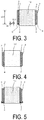
FIG. 3 is a drawing illustrating another example of a cross-section cut along line A-A depicted inFIG. 1A . -
FIG. 4 is a drawing illustrating another example of a cross-section cut along line A-A depicted inFIG. 1A . -
FIG. 5 is a drawing illustrating another example of a cross-section cut along line A-A depicted inFIG. 1A . -
FIG. 6 is a schematic cross-sectional view illustrating an example of an embodiment of an injection device of the invention. -
FIG. 7 is a schematic block diagram illustrating an example of an embodiment of a fuel-injection system of the invention. -
FIG. 8A is a schematic vertical cross-sectional view illustrating an example of an embodiment of a conventional multi-layer piezoelectric element.FIG. 8B is a drawing illustrating an example of a cross-section cut along line A-A depicted inFIG. 8A . - Hereinafter, a description of examples of an embodiment of a multi-layer piezoelectric element of the invention is given while referencing the drawings.
-
FIG. 1A is a schematic vertical cross-sectional view illustrating an example of an embodiment of the multi-layer piezoelectric element of the invention.FIG. 1B is a drawing illustrating an example of a cross-section cut along line A-A depicted inFIG. 1A . - The multi-layer
piezoelectric element 1 illustrated inFIGS. 1A and 1B includes a stackedbody 10 in whichpiezoelectric layers 11 andinternal electrode layers 12 are laminated, anexternal electrode plate 2 connected to a side surface of the stackedbody 10 and electrically connected to theinternal electrode layers 12, and an electricallyconductive bonding material 3 disposed between the side surface of the stackedbody 10 and one main surface of theexternal electrode plate 2. A resin layer 4 is disposed on at least one end of a space between the side surface of thestacked body 10 and the one main surface of theexternal electrode plate 2 in a width direction in a cross-sectional view perpendicular to the side surface of thestacked body 10. - The
stacked body 10 constituting the multi-layerpiezoelectric element 1 includes anactive section 13 in which thepiezoelectric layers 11 and theinternal electrode layers 12 are laminated; andinactive sections 14, located outside theactive section 13, made from thepiezoelectric layers 11 disposed at both ends in a stacking direction of the stackedbody 10. Thestacked body 10 is formed into a rectangular parallelepiped shape having, for example, a length of 0.5 to 10 mm, a width of 0.5 to 10 mm, and a height of 1 to 100 mm. - The
piezoelectric layers 11 constituting the stackedbody 10 are formed from a ceramic having piezoelectric properties. Examples of such a ceramic that can be used include perovskite-type oxides made from lead zirconate titanate (PbZrO3-PbTiO3), lithium niobate (LiNbO3), lithium tantalate (LiTaO3), and the like. A thickness of each of thepiezoelectric layers 11 is, for example, from 3 to 250 µm. - The
internal electrode layers 12 constituting the stackedbody 10 are formed by firing with the ceramics that forms thepiezoelectric layers 11 at the same time. Theinternal electrode layers 12 are alternately laminated with thepiezoelectric layers 11 so as to be over and under thepiezoelectric layers 11, and apply driving voltage to thepiezoelectric layers 11 sandwiched therebetween due to positive electrodes and negative electrodes being arranged in the lamination order. Examples of materials that can be used for forming theinternal electrode layers 12 include electrical conductors having silver-palladium alloys, which have low reactivity with piezoelectric ceramics, as a primary component, or electrical conductors containing copper, platinum, or the like. In the example illustrated inFIGS. 1A and 1B , each of the positive electrodes and the negative electrodes lead out alternately to a pair of opposing side surfaces of thestacked body 10, and are electrically connected to a pair of electricallyconductive bonding materials 3 disposed on the side surfaces of thestacked body 10. A thickness of each of theinternal electrode layers 12 is, for example, from 0.1 to 5 µm. - Additionally, the
external electrode plate 2 is connected to the side surface of thestacked body 10 with the electricallyconductive bonding material 3 interposed therebetween, and theexternal electrode plate 2 is electrically connected to theinternal electrode layers 12. Specifically, each of the pair ofexternal electrode plates 2 is disposed on each of the pair of opposing side surfaces of thestacked body 10, is electrically connected to theinternal electrode layers 12 via the electricallyconductive bonding material 3, and a portion thereof extends past one edge of thestacked body 10 in the stacking direction. The pair ofexternal electrode plates 2 is made from a flat metal plate of copper, iron, stainless steel, phosphor bronze, or the like and is formed, for example, having a width of 0.5 to 10 mm and a thickness of 0.1 to 0.3 mm. In addition to flat metal plates, in order to obtain a benefit of mitigating stress generated by the expansion and contraction of thestacked body 1, metal plates machined into, for example, a form having slits in the horizontal direction or a reticulated form may be used as theexternal electrode plates 2. - The electrically
conductive bonding material 3 is disposed between each of the side surfaces of the stackedbody 10 and the one main surface of each of theexternal electrode plates 2, from theactive section 13 to theinactive sections 14; and is electrically connected to theexternal electrode plates 2 and the ends of the internal electrode layers 12 leading out to the side surfaces of the stackedbody 10. The electricallyconductive bonding material 3 is preferably made from an electrically conductive adhesive made from, for example, an epoxy resin or a polyimide resin containing metal powder with excellent electrical conductivity such as Ag powder, Cu powder, or the like. In a cross-sectional view of the electricallyconductive bonding material 3 perpendicular to the side surfaces of the stackedbody 10, the electricallyconductive bonding material 3 is formed with a thickness of 5 to 70 µm. - Note that while not illustrated in the drawings, an electrical conductor layer electrically connected to the ends of the internal electrode layers 12 may be disposed on the side surfaces of the stacked
body 10, and this electrical conductor layer may be connected to each of theexternal electrode plates 2 by disposing the electricallyconductive bonding material 3 on a surface of the electrical conductor layer. - Moreover, as illustrated in
FIG. 1B , the resin layer 4 is disposed on at least one end of the space between each of the side surfaces of the stackedbody 10 and the one main surface of each of theexternal electrode plates 2 in the width direction in a cross-sectional view perpendicular to the side surface of the stackedbody 10. Herein, the resin layer 4 is a layer formed from a resin free of electrical conductive particles. Preferable examples of the resin forming the resin layer 4 include epoxy, acrylic, and imide resins. Furthermore, in cases where the electricallyconductive bonding material 3 is made from an electrical conductive adhesive containing a resin, a material that is different from the resin forming the electrically conductive adhesive may be selected as the resin forming the resin layer 4 so as to align the coefficients of thermal expansion of the electricallyconductive bonding material 3 and the resin layer 4. As a result of such selection, the load applied to the electricallyconductive bonding material 3 due to thermal stress can be reduced. Note that, "in a cross-sectional view of the electricallyconductive bonding material 3 perpendicular to the side surfaces of the stackedbody 10" means viewing the electricallyconductive bonding material 3 from the stacking direction (the vertical direction inFIG. 1A ). Additionally, the "one main surface of theexternal electrode plate 2" refers to the main surface on a side of the stackedbody 10 facing thestacked body 10, and the main surface primarily bonded to the electricallyconductive bonding material 3. - The resin layer 4 is a constituent that is disposed so as to extend in the stacking direction on at least one end of the space between each of the side surfaces of the stacked
body 10 and the one main surface of each of theexternal electrode plates 2 in the width direction. In a cross-sectional view of the electricallyconductive bonding material 3 perpendicular to the side surfaces of the stackedbody 10, as illustrated inFIG. 1B , thestacked body 10 has a configuration in which the resin layer 4 is disposed on at least one end of the space between each of the side surfaces of the stackedbody 10 and the one main surface of each of theexternal electrode plates 2 in the width direction. - The resin layer 4 is bonded to each of the side surfaces of the stacked
body 10 and is also bonded to the one main surface of the each of theexternal electrode plates 2. A width W1 of the resin layer 4 disposed on the end of the space between each of the side surfaces of the stackedbody 10 and the one main surface of each of theexternal electrode plates 2 in the width direction is set to a length of, for example, 2 to 40% of a width W2 of theexternal electrode plates 2. Note that the resin layer 4 may protrude from between the side surface of the stackedbody 10 and the one main surface of theexternal electrode plate 2, and the width W1 does not include the length of the portion protruding from between the side surface of the stackedbody 10 and the one main surface of theexternal electrode plate 2. - With the configuration described above, stress applied on at least one end of the space between the side surfaces of the stacked
body 10 and the one main surface of each of theexternal electrode plates 2 in the width direction is applied to the resin layer 4. As a result, the stress applied to the electricallyconductive bonding material 3 is reduced and the formation of cracks in the electricallyconductive bonding material 3 is suppressed. Therefore, a multi-layerpiezoelectric element 1 with improved durability can be obtained. - In cases where the electrically
conductive bonding material 3 is an electrically conductive adhesive containing a resin, preferably the resin layer 4 is provided as a constituent separate from the electrically conductive bonding material 3 (the electrically conductive adhesive) and a boundary between these two constituents exists. With such a configuration, even if cracking occurs in the resin layer 4, progression of the cracking to the electricallyconductive bonding material 3 can be suppressed. Additionally, in cases where the electricallyconductive bonding material 3 is an electrically conductive adhesive containing a resin, and this resin is the same as the resin forming the resin layer 4, the boundary therebetween will be unclear. In such a case, the boundary is defined by a line formed by connecting electrically conductive particles, from among the electrically conductive particles forming the electricallyconductive bonding material 3, located at an edge on the resin layer 4 side. Here, the boundary may be formulated by combining a vertical cross-section cut parallel with theexternal electrode plate 2 and a horizontal cross-section cut perpendicularly to theexternal electrode plate 2. - Moreover, as illustrated in
FIG. 2 , in a cross-sectional view perpendicular to the side surfaces of the stackedbody 10, the resin layer 4 is preferably also disposed at the other end of the space between each of the side surfaces of the stackedbody 10 and the one main surface of each of theexternal electrode plates 2 in the width direction. In other words, the resin layer 4 is preferably disposed at both ends of the space between each of the side surfaces of the stackedbody 10 and the one main surface of each of theexternal electrode plates 2 in the width direction. As a result of the resin layer 4 being provided at both ends of the space between each of the side surfaces of the stackedbody 10 and the one main surface of each of theexternal electrode plates 2 in the width direction, stress applied to the electricallyconductive bonding material 3 is further mitigated and durability is further improved. - Here, the width W1 of each of the resin layers 4, disposed at each of the ends of the space between each of the side surfaces of the stacked
body 10 and the one main surface of each of theexternal electrode plates 2 in the width direction, is set to a length of, for example, 2 to 20% of the width W2 of theexternal electrode plates 2. - Furthermore, as illustrated in
FIG. 3 , in a cross-sectional view perpendicular to the side surfaces of the stackedbody 10, agap 5 preferably is located between the electricallyconductive bonding material 3 and the resin layer 4 disposed on at least one end of the space between each of the side surfaces of the stackedbody 10 and the one main surface of each of theexternal electrode plates 2 in the width direction. Due to the presence of thegap 5, the progression of cracks that has occurred due to stress being applied to the resin layer 4 will stop at thegap 5 and cracks will not progress to the electricallyconductive bonding material 3, leading to further improvements in durability. - Note that a width W3 of the
gap 5 disposed between the resin layer 4 and the electricallyconductive bonding material 3 is set to a length of, for example, 2 to 20% of the width W2 of theexternal electrode plates 2. Additionally, in cases where the resin layer 4 is disposed on each end of the space between each of the side surfaces of the stackedbody 10 and the one main surface of each of theexternal electrode plates 2 in the width direction, and thegap 5 is disposed between the electricallyconductive bonding material 3 and each of the resin layers 4, the width W3 of each of thegaps 5 is set to a length of, for example, 1 to 10% of the width W2 of theexternal electrode plates 2. - Additionally, as illustrated in
FIG. 4 , in a cross-sectional view perpendicular to the side surfaces of the stackedbody 10, the resin layer 4 preferably extends to a side surface of theexternal electrode plate 2. Due to the presence of the resin layer 4 extending to the side surface of theexternal electrode plate 2, the resin layer 4 will cover the edge of theexternal electrode plate 2 where stress concentrates and, as a result, cracking is suppressed. Furthermore, even if cracks occur from an edge of the interface between the side surface of theexternal electrode plate 2 and the resin layer 4, distance to the electricallyconductive bonding material 3 is increased and, therefore, the progression of the cracks to the electricallyconductive bonding material 3 is suppressed, leading to further improvements in durability. - Additionally, as illustrated in
FIG. 5 , in a cross-sectional view perpendicular to the side surfaces of the stackedbody 10, the resin layer 4 is preferably formed up to a portion of the other main surface of theexternal electrode plate 2. Due to the presence of the resin layer 4 on a portion of the other main surface of theexternal electrode plate 2, the distance of cracks, which occur from the edge of the interface between theexternal electrode plate 2 and the resin layer 4, to the electricallyconductive bonding material 3 is increased further and, therefore, the progression of the cracks to the electricallyconductive bonding material 3 is suppressed, leading to further improvements in durability. Herein, "the other main surface of theexternal electrode plate 2" means the main surface on the side opposite thestacked body 10. - Note that the resin layer 4 may be disposed so as to protrude from between each of the side surfaces of the stacked
body 10 and the one main surface of each of theexternal electrode plates 2, and cover theexternal electrode plates 2. - Additionally, the resin layer 4 may be disposed so as to protrude from between each of the side surfaces of the stacked
body 10 and the one main surface of each of theexternal electrode plates 2, and cover the side surfaces of the stackedbody 10. That is, there are cases where a cover layer is disposed so as to cover the side surfaces of the stackedbody 10 to suppress creeping discharge and migration and to protect the stacked body and the like and, in cases where this cover layer is made from a resin, the cover layer may penetrate between each of the side surfaces of the stackedbody 10 and the one main surface of each of theexternal electrode plates 2. As such, beneficial effects will be obtained in that adhesiveness of the cover layer will increase and cracking of the electricallyconductive bonding material 3 will be suppressed. - Next, a manufacturing method of the multi-layer
piezoelectric element 1 according to the embodiment will be described. - First, ceramic green sheets that will become the
piezoelectric layers 11 are fabricated. Specifically, a ceramic slurry is formed by mixing a calcined powder of piezoelectric ceramics, a binder made from an acrylic-based, butyral-based, or similar organic polymer, and a plasticizer. Then, the ceramic green sheets are fabricated using this ceramic slurry by utilizing a doctor blade method, a calender roll method, or similar tape molding method. Any piezoelectric ceramics may be used, provided that the piezoelectric ceramics have piezoelectric properties, and examples thereof include, perovskite-type oxides made from lead zirconate titanate (PbZrO3-PbTiO3) and the like. Additionally, dibutyl phthalate (DBP), dioctyl phthalate (DOP), or the like may be used as the plasticizer. - Next, an electrically conductive paste that becomes the internal electrode layers 12 is fabricated. Specifically, an electrically conductive paste is fabricated by adding/blending a binder and a plasticizer to a silver-palladium metal alloy powder. This electrically conductive paste is applied in the pattern of the internal electrode layers 12 on the ceramic green sheets using a screen printing method. Furthermore, a plurality of the ceramic green sheets on which the electrically conductive paste is printed are laminated and subjected to binder removal treatment at a predetermined temperature. Thereafter, firing at a temperature of 900 to 1,200°C is performed and the resulting products are subjected to grinding processing into a predetermined shape using a surface grinding machine or the like. Thus, the
active section 13 in which thepiezoelectric layers 11 and the internal electrode layers 12 are alternately laminated is fabricated. Theinactive sections 14 are fabricated by laminating sheets on which the electrically conductive paste that becomes the internal electrode layers 12 is not applied. Thestacked body 10 is manufactured by assembling theactive section 13 and theinactive sections 14. - Note that the
stacked body 10 is not limited to products fabricated according to the manufacturing method described above and, provided that thestacked body 10 formed by laminating a plurality of thepiezoelectric layers 11 and the internal electrode layers 12 together can be fabricated, any manufacturing method may be used to fabricate thestacked body 10. - Next, the
external electrode plates 2 are connected and fixed to the side surfaces of the stackedbody 10 with the electricallyconductive bonding material 3 interposed therebetween. - An adhesive made from an epoxy resin or a polyimide resin containing metal powder with excellent electrical conductivity such as Ag powder, Cu powder, or the like, is used as the electrically
conductive bonding material 3 and is formed with a thickness of 5 to 70 µm. The electricallyconductive bonding material 3 can be formed so as to be restrained to a predetermined thickness and width by using a screen printing method or dispensing system. - Note that when employing screen printing, an example of a method for providing a place for applying the resin layer 4 includes providing a printing plate for screen printing with predetermined holes and printing. Additionally, when employing a dispensing system, an example of a method for providing a place for applying the resin layer 4 includes using a dispenser that has a needle diameter conforming to the desired application width, not applying material at the place where the resin layer 4 will be applied, and only dispensing material at the desired locations.
- The
external electrode plates 2 are made from a flat metal plate of copper, iron, stainless steel, phosphor bronze, or the like and are formed, for example, having a width of 0.5 to 10 mm and a thickness of 0.1 to 0.3 mm. Here, examples of methods used to form theexternal electrode plates 2 into a form having slits in the horizontal direction or a reticulated form include punching using a punching die, laser machining and the like; and a bending die may be used to make curved or bent forms. - Next, the resin layer 4 is applied on the end of the space in the width direction of each of the side surfaces of the stacked
body 10 and theexternal electrode plates 2. The resin layer 4 can be formed by using, for example, an epoxy, acrylic, or imide resin and restraining such formation to a predetermined location and amount by using a dispensing system. - Then, a direct electric field of 0.1 to 3 kV/mm is applied to the
external electrode plates 2, and thepiezoelectric layers 11 constituting the stackedbody 10 are polarized. Thus, the multi-layerpiezoelectric element 1 is completed. With this multi-layerpiezoelectric element 1, by connecting an external power supply via theexternal electrode plates 2 and applying voltage to thepiezoelectric layers 11, each of thepiezoelectric layers 11 can be greatly displaced due to the inverse piezoelectric effect. As a result, it is possible to cause the multi-layerpiezoelectric element 1 to function as, for example, a fuel injection valve for an automobile that injects/supplies fuel to an engine. - Next, an example of an embodiment of the injection device of the invention is described.
FIG. 6 is a schematic cross-section view illustrating an example of an embodiment of the injection device of the invention. - As illustrated in
FIG. 6 , theinjection device 19 of this embodiment is constituted by a housing container (container) 23 including aninjection hole 21 at one end thereof, and the multi-layerpiezoelectric element 1 of the embodiment described above is contained inside thehousing container 23. - A
needle valve 25 capable of opening and closing theinjection hole 21 is provided in thehousing container 23. Afluid passage 27 is provided in theinjection hole 21 that is capable of communication with theinjection hole 21 depending on movement of theneedle valve 25. Thefluid passage 27 is connected to an external fluid supply source, which supplies fluid at constant high pressure to thefluid passage 27. Thus, theinjection device 19 is configured so that, when theneedle valve 25 opens theinjection hole 21, the fluid supplied to thefluid passage 27 is discharged out or into an adjacent container, for example, a combustion chamber of an internal combustion engine (not illustrated in the drawings), from theinjection hole 21. - The diameter of an upper end portion of the
needle valve 25 is larger and constitutes apiston 31 that is slideable in acylinder 29 formed in thehousing container 23. Moreover, the multi-layerpiezoelectric element 1 of the example described above is contained in thehousing container 23 in contact with thepiston 31. - In the
injection device 19 described above, when voltage is applied and the multi-layerpiezoelectric element 1 elongates, pressure is applied to thepiston 31 and theneedle valve 25 closes thefluid passage 27 that communicates with theinjection hole 21. Thus, the supply of fluid is halted. Additionally, theinjection device 19 is configured so that when the application of voltage is halted, the multi-layerpiezoelectric element 1 contracts, aplate spring 33 pushes thepiston 31 back, thefluid passage 27 is opened, theinjection hole 21 communicates with thefluid passage 27, and the fluid is sprayed from theinjection hole 21. - Note that the
injection device 19 may be configured so that thefluid passage 27 opens when voltage is applied to the multi-layerpiezoelectric element 1 and thefluid passage 27 closes when the application of voltage is halted. - Additionally, the
injection device 19 of this embodiment may be configured to include acontainer 23 including aninjection hole 21 and the multi-layerpiezoelectric element 1 of the embodiment described above, wherein theinjection device 19 is configured to discharge the fluid filling thecontainer 23 through theinjection hole 21 by driving the multi-layerpiezoelectric element 1. That is, it is not necessary for the multi-layerpiezoelectric element 1 to be inside thecontainer 23 and any configuration is possible provided that pressure is applied to the inside of thecontainer 23, to control the injection of the fluid, by the driving of the multi-layerpiezoelectric element 1. Note that in theinjection device 19 of this embodiment, the term "fluid" should be construed to include various types of liquids such as electrically conductive paste and the like and also gases, in addition to fuel, ink, and the like. By using theinjection device 19 of this embodiment, the flow rate and spray timing of the fluid can be stably controlled over an extended period of time. - By using the
injection device 19 of this embodiment utilizing the multi-layerpiezoelectric element 1 of this embodiment in an internal combustion engine, compared to conventional injection devices, theinjection device 19 can be made to inject fuel into the combustion chamber of an internal combustion engine such as an engine with high precision over an extended period of time. - Next, an example of an embodiment of the fuel-injection system of the invention is described.
FIG. 7 is a schematic diagram illustrating an example of an embodiment of the fuel-injection system of the invention. - As illustrated in
FIG. 7 , a fuel-injection system 35 of this embodiment includes acommon rail 37 configured to store high-pressure fuel as a high-pressure fluid, a plurality of theinjection device 19 of the embodiment described above configured to inject the high-pressure fluid stored in thecommon rail 37, apressure pump 39 configured to supply the high-pressure fluid to thecommon rail 37, and aninjection control unit 41 configured to send driving signals to theinjection device 19. - The
injection control unit 41 controls an amount and timing of the injection of the high-pressure fluid on the basis of external information or signals from external sources. For example, in cases where the fuel-injection system 35 of this embodiment is used for fuel injection in an engine, the amount and timing of fuel injection can be controlled while using a sensor or the like to sense the condition within the combustion chamber of the engine. Thepressure pump 39 serves a role of supplying fluid fuel from afuel tank 43 to thecommon rail 37 at high pressure. For example, in a case of the fuel-injection system 35 of an engine, fluid fuel is pumped to thecommon rail 37 at high pressures from 1000 to 2000 atmospheres (about 101 MPa to about 203 MPa), and preferably from 1500 to 1700 atmospheres (about 152 MPa to about 172 MPa). The high-pressure fuel supplied from thepressure pump 39 is stored in thecommon rail 37 and pumped appropriately to theinjection device 19. As described previously, theinjection device 19 sprays the prescribed fluid out or into an adjacent container from theinjection hole 21. For example, in cases where an engine is the target of the injection/supplying of fuel, a high-pressure fuel is sprayed as a mist from theinjection hole 21 into the combustion chamber of the engine. - According to the fuel-
injection system 35 of this embodiment, desired injection of high-pressure fuel can be stably performed over an extended period of time. - Next, examples of the invention are described.
- The multi-layer piezoelectric element of the invention was fabricated as described below. First, a calcined powder of piezoelectric ceramics having lead zirconate titanate (PbZrO3-PbTiO3) with an average particle size of 0.4 µm as a primary component, a binder, and a plasticizer were blended. Thus, a ceramic slurry was obtained. Then, using this ceramic slurry, ceramic green sheets of a thickness of 50 µm that would become the piezoelectric layers were fabricated via a doctor blade method.
- Then, a binder was added to silver-palladium alloy and an electrically conductive paste that would become the internal electrode layers was fabricated.
- Next, the electrically conductive paste that would become the internal electrode layers was printed via a screen printing method on one side of the ceramic green sheets, and 200 of the ceramic green sheets, on which the electrically conductive paste was printed, were laminated together. Additionally, a total of 15 ceramic green sheets, on which the electrically conductive paste that would become the internal electrode layers was not printed, were laminated on top of and under the body of 200 ceramic green sheets, on which the electrically conductive paste that would become the internal electrode layers was printed. Then, firing at 980 to 1100°C was performed and the resulting product was ground into a predetermined shape using a surface grinding machine. Thus, a 5 mm square stacked body was obtained.
- Next, an electrically conductive bonding material constituted by a paste-like mixture of Ag powder and polyimide resin was applied to a front surface of the stacked body and the external electrode plates were attached and affixed to the front surface of the stacked body.
- Next, using a dispenser, the epoxy resin was applied on an end in the width direction between each of the side surfaces of the stacked body and each of the external electrode plates.
- A multi-layer piezoelectric element was fabricated as a
Sample 1 using external electrode plates made from phosphor bronze having the cross-section illustrated inFIG. 1A , a thickness of 0.1 mm, and a width of 4.0 mm. An electrically conductive bonding material made from silver polyimide was applied so as to form an electrically conductive bonding material layer between each side surface of the active section and each of the external electrode plates; and had a structure provided with a thickness of 0.03 mm. Specifically, the width of the electrically conductive bonding material to be dispensed from the nozzle diameter of the dispenser was set to be 3.0 mm and the electrically conductive bonding material was applied so that the cross-section illustrated inFIG. 1B was formed. Furthermore, the epoxy resin was applied using the dispenser to one end of the space between each side surface of the stacked body and each of the external electrode plates in the width direction, and the width thereof was 1.0 mm. - Additionally, a multi-layer piezoelectric element was fabricated as a
Sample 2 using external electrode plates made from phosphor bronze having the cross-section illustrated inFIG. 2 , a thickness of 0.1 mm, and a width of 4.0 mm. Specifically, the electrically conductive bonding material was applied to a center of the external electrode plates at a thickness of 0.03 mm and a width of 3.0 mm so that the resin could be applied, using a dispenser, on both ends of the space between each of the side surfaces of the stacked body and each of the external electrode plates in the width direction. Furthermore, the epoxy resin was applied, using a dispenser, on both ends in the width direction between each of the side surfaces of the stacked body and each of the external electrode plates, and the width at each end thereof was 0.5 mm. - Additionally, a multi-layer piezoelectric element was fabricated as a
Sample 3 using external electrode plates made from phosphor bronze having the cross-section illustrated inFIG. 3 , a thickness of 0.1 mm, and a width of 4.0 mm. Specifically, the electrically conductive bonding material was applied using a dispenser at a thickness of 0.03 mm and a width of 3.0 mm. Furthermore, the epoxy resin was applied, using a dispenser, one end of the space between each of the side surfaces of the stacked body and each of the external electrode plates in the width direction, and the width thereof was 0.5 mm. Here, the position of the dispenser for applying the epoxy resin was adjusted so as to provide a gap between the electrically conductive bonding material and the epoxy resin, and a gap of 0.5 mm was provided. - Additionally, a multi-layer piezoelectric element was fabricated as a Sample 4 using external electrode plates made from phosphor bronze having the cross-section illustrated in
FIG. 4 , a thickness of 0.1 mm, and a width of 4.0 mm. Specifically, the electrically conductive bonding material was applied using a dispenser at a thickness of 0.03 mm and a width of 3.0 mm. Furthermore, the epoxy resin was applied using the dispenser to one end of the space between each side surface of the stacked body and each of the external electrode plates in the width direction, and the width thereof was 1.0 mm. Here, the amount of the epoxy resin was adjusted so as to cover 0.05 mm of the thickness of the side surface of the external electrode plates. - Additionally, a multi-layer piezoelectric element was fabricated as a
Sample 5 using external electrode plates made from phosphor bronze having the cross-section illustrated inFIG. 5 , a thickness of 0.1 mm, and a width of 4.0 mm. Specifically, the electrically conductive bonding material was applied using a dispenser at a thickness of 0.03 mm and a width of 3.0 mm. Furthermore, the epoxy resin was applied using the dispenser to one end of the space between each side surface of the stacked body and each of the external electrode plates in the width direction, and the width thereof was 1.0 mm. Here, the amount of the epoxy resin was adjusted so as to cover all of the side surface of the external electrode plates and to cover 1.0 mm of a top surface of the external electrode plates. - Additionally, a multi-layer piezoelectric element (Sample 6) was fabricated as a Comparative Example using external electrode plates having the cross-section illustrated in
FIGS. 8A and 8B . Here, external electrode plates having a thickness of 0.1 mm and a width of 4.0 mm were used, and the electrically conductive bonding material was provided so that a thickness thereof was 0.03 mm and a width thereof was 4 mm. - These multi-layer piezoelectric elements were subjected to polarization treatment by applying a direct electric field of 3 kV/mm for 15 minutes to the external electrode plate via a lead member welded and connected to the external electrode plate. Upon the application of 160 V of direct current voltage to the multi-layer piezoelectric elements, displacement in an amount of 30 µm in the stacking direction of the stacked body was obtained.
- Furthermore, 0 V to 160 V of alternating current was applied at a frequency of 150 Hz in a 30°C, 90% humidity environment, and a durability test for continuous driving was performed.
- As a result, with the multi-layer piezoelectric element of the Comparative Example, namely Sample 6, detachment of the external electrode plates occurred at 1 × 10⁴ continuous drives and the driving thereof halted at 1 × 10⁵ continuous drives.
- In contrast, with the multi-layer piezoelectric element of
Samples - It is clear from the results described above that, according to the present invention, a multi-layer piezoelectric element with improved long-term durability can be realized.
-
- 1
- Multi-layer piezoelectric element
- 10
- Stacked body
- 11
- Piezoelectric layer
- 12
- Internal electrode layer
- 13
- Active section
- 14
- Inactive section
- 2
- External electrode plate
- 3
- Electrically Conductive bonding material
- 4
- Resin layer
- 5
- Gap
Claims (7)
- A multi-layer piezoelectric element comprising:a stacked body comprising piezoelectric layers and internal electrode layers laminated together;an external electrode plate connected to a side surface of the stacked body and electrically connected to the internal electrode layers; andan electrically conductive bonding material disposed between the side surface of the stacked body and one main surface of the external electrode plate; whereina resin layer is disposed on at least one end of a space between the side surface of the stacked body and the one main surface of the external electrode plate in a width direction in a cross-sectional view perpendicular to the side surface of the stacked body.
- The multi-layer piezoelectric element according to claim 1, wherein the resin layer is disposed on both ends of the space between the side surface of the stacked body and the one main surface of the external electrode plate in the width direction.
- The multi-layer piezoelectric element according to claim 1 or 2, wherein a gap is located between the electrically conductive bonding material and the resin layer.
- The multi-layer piezoelectric element according to any one of claims 1 to 3, wherein the resin layer extends to the side surface of the external electrode plate.
- The multi-layer piezoelectric element according to any one of claims 1 to 3, wherein the resin layer comprises a portion coming around onto the other main surface of the external electrode plate.
- An injection device comprising:a container comprising an injection hole; andthe multi-layer piezoelectric element according to any one of claims 1 to 5, whereinthe injection device is configured to discharge a fluid stored within the container through the injection hole by driving the multi-layer piezoelectric element.
- A fuel-injection system comprising:a common rail for storing high-pressure fuel;the injection device according to claim 6 for injecting the high-pressure fuel stored in the common rail;a pressure pump for supplying the high-pressure fuel to the common rail; andan injection control unit for sending driving signals to the injection device.
Applications Claiming Priority (2)
| Application Number | Priority Date | Filing Date | Title |
|---|---|---|---|
| JP2014014427 | 2014-01-29 | ||
| PCT/JP2014/075463 WO2015114879A1 (en) | 2014-01-29 | 2014-09-25 | Laminated piezoelectric element, and injection device and fuel injection system provided with same |
Publications (3)
| Publication Number | Publication Date |
|---|---|
| EP3101702A1 true EP3101702A1 (en) | 2016-12-07 |
| EP3101702A4 EP3101702A4 (en) | 2017-10-18 |
| EP3101702B1 EP3101702B1 (en) | 2020-03-18 |
Family
ID=53756479
Family Applications (1)
| Application Number | Title | Priority Date | Filing Date |
|---|---|---|---|
| EP14881111.0A Active EP3101702B1 (en) | 2014-01-29 | 2014-09-25 | Laminated piezoelectric element, and injection device and fuel injection system provided with same |
Country Status (3)
| Country | Link |
|---|---|
| EP (1) | EP3101702B1 (en) |
| JP (1) | JP6185609B2 (en) |
| WO (1) | WO2015114879A1 (en) |
Family Cites Families (5)
| Publication number | Priority date | Publication date | Assignee | Title |
|---|---|---|---|---|
| JP2005223014A (en) | 2004-02-03 | 2005-08-18 | Denso Corp | Multilayer piezoelectric element and method for manufacturing the same |
| JP2006303044A (en) * | 2005-04-18 | 2006-11-02 | Denso Corp | Multilayer piezoelectric element |
| JP4929875B2 (en) * | 2006-06-30 | 2012-05-09 | 株式会社デンソー | Multilayer piezoelectric element |
| WO2012057327A1 (en) * | 2010-10-28 | 2012-05-03 | 京セラ株式会社 | Laminated piezoelectric element, injection device using same, and fuel injection system |
| WO2013031727A1 (en) * | 2011-08-30 | 2013-03-07 | 京セラ株式会社 | Laminated piezoelectric element and piezoelectric actuator, injection device, and fuel injection system provided with same |
-
2014
- 2014-09-25 EP EP14881111.0A patent/EP3101702B1/en active Active
- 2014-09-25 JP JP2015559735A patent/JP6185609B2/en active Active
- 2014-09-25 WO PCT/JP2014/075463 patent/WO2015114879A1/en not_active Ceased
Also Published As
| Publication number | Publication date |
|---|---|
| WO2015114879A1 (en) | 2015-08-06 |
| JP6185609B2 (en) | 2017-08-23 |
| EP3101702B1 (en) | 2020-03-18 |
| EP3101702A4 (en) | 2017-10-18 |
| JPWO2015114879A1 (en) | 2017-03-23 |
Similar Documents
| Publication | Publication Date | Title |
|---|---|---|
| CN103098251A (en) | Laminated piezoelectric element, injection device using same, and fuel injection system | |
| JP5787547B2 (en) | Multilayer piezoelectric element, injection device including the same, and fuel injection system | |
| WO2013115341A1 (en) | Laminated piezoelectric element, injection device provided with same, and fuel injection system | |
| CN104350624B (en) | Piezoelektrisches mehrschichtelement and possess its piezo-activator, injection apparatus and fuel injection system | |
| JP5813235B2 (en) | Multilayer piezoelectric element, piezoelectric actuator including the same, injection device, and fuel injection system | |
| JP6196134B2 (en) | Multilayer piezoelectric element, injection device including the same, and fuel injection system | |
| EP3101701B1 (en) | Laminated piezoelectric element, and injection device and fuel-injection system containing said laminated piezoelectric element | |
| EP3101702B1 (en) | Laminated piezoelectric element, and injection device and fuel injection system provided with same | |
| JP5744242B2 (en) | Multilayer piezoelectric element, injection device including the same, and fuel injection system | |
| JP6259092B2 (en) | Multilayer piezoelectric element, injection device including the same, and fuel injection system | |
| JP5701397B2 (en) | Multilayer piezoelectric element, piezoelectric actuator including the same, injection device, and fuel injection system | |
| JP6062728B2 (en) | Multilayer piezoelectric element, injection device including the same, and fuel injection system | |
| CN104160524B (en) | Piezoelektrisches mehrschichtelement and possess its injection apparatus and fuel injection system | |
| JP2017011125A (en) | Lamination type piezoelectric element and injection device including the same and fuel injection system | |
| JP6017937B2 (en) | Multilayer piezoelectric element, injection device including the same, and fuel injection system | |
| JP2018206801A (en) | Multilayer piezoelectric element, injection device including the same, and fuel injection system |
Legal Events
| Date | Code | Title | Description |
|---|---|---|---|
| PUAI | Public reference made under article 153(3) epc to a published international application that has entered the european phase |
Free format text: ORIGINAL CODE: 0009012 |
|
| STAA | Information on the status of an ep patent application or granted ep patent |
Free format text: STATUS: REQUEST FOR EXAMINATION WAS MADE |
|
| 17P | Request for examination filed |
Effective date: 20160616 |
|
| AK | Designated contracting states |
Kind code of ref document: A1 Designated state(s): AL AT BE BG CH CY CZ DE DK EE ES FI FR GB GR HR HU IE IS IT LI LT LU LV MC MK MT NL NO PL PT RO RS SE SI SK SM TR |
|
| AX | Request for extension of the european patent |
Extension state: BA ME |
|
| DAX | Request for extension of the european patent (deleted) | ||
| RIN1 | Information on inventor provided before grant (corrected) |
Inventor name: ASAKURA, YASUHIRO |
|
| A4 | Supplementary search report drawn up and despatched |
Effective date: 20170915 |
|
| RIC1 | Information provided on ipc code assigned before grant |
Ipc: H01L 41/047 20060101AFI20170911BHEP Ipc: H01L 41/09 20060101ALI20170911BHEP Ipc: H01L 41/053 20060101ALI20170911BHEP Ipc: F02M 51/06 20060101ALI20170911BHEP Ipc: H01L 41/083 20060101ALI20170911BHEP |
|
| GRAP | Despatch of communication of intention to grant a patent |
Free format text: ORIGINAL CODE: EPIDOSNIGR1 |
|
| STAA | Information on the status of an ep patent application or granted ep patent |
Free format text: STATUS: GRANT OF PATENT IS INTENDED |
|
| INTG | Intention to grant announced |
Effective date: 20191009 |
|
| GRAS | Grant fee paid |
Free format text: ORIGINAL CODE: EPIDOSNIGR3 |
|
| GRAA | (expected) grant |
Free format text: ORIGINAL CODE: 0009210 |
|
| STAA | Information on the status of an ep patent application or granted ep patent |
Free format text: STATUS: THE PATENT HAS BEEN GRANTED |
|
| RAP1 | Party data changed (applicant data changed or rights of an application transferred) |
Owner name: KYOCERA CORPORATION |
|
| AK | Designated contracting states |
Kind code of ref document: B1 Designated state(s): AL AT BE BG CH CY CZ DE DK EE ES FI FR GB GR HR HU IE IS IT LI LT LU LV MC MK MT NL NO PL PT RO RS SE SI SK SM TR |
|
| REG | Reference to a national code |
Ref country code: GB Ref legal event code: FG4D |
|
| REG | Reference to a national code |
Ref country code: DE Ref legal event code: R096 Ref document number: 602014062692 Country of ref document: DE |
|
| REG | Reference to a national code |
Ref country code: AT Ref legal event code: REF Ref document number: 1246944 Country of ref document: AT Kind code of ref document: T Effective date: 20200415 Ref country code: IE Ref legal event code: FG4D |
|
| PG25 | Lapsed in a contracting state [announced via postgrant information from national office to epo] |
Ref country code: RS Free format text: LAPSE BECAUSE OF FAILURE TO SUBMIT A TRANSLATION OF THE DESCRIPTION OR TO PAY THE FEE WITHIN THE PRESCRIBED TIME-LIMIT Effective date: 20200318 Ref country code: FI Free format text: LAPSE BECAUSE OF FAILURE TO SUBMIT A TRANSLATION OF THE DESCRIPTION OR TO PAY THE FEE WITHIN THE PRESCRIBED TIME-LIMIT Effective date: 20200318 Ref country code: NO Free format text: LAPSE BECAUSE OF FAILURE TO SUBMIT A TRANSLATION OF THE DESCRIPTION OR TO PAY THE FEE WITHIN THE PRESCRIBED TIME-LIMIT Effective date: 20200618 |
|
| REG | Reference to a national code |
Ref country code: NL Ref legal event code: MP Effective date: 20200318 |
|
| PG25 | Lapsed in a contracting state [announced via postgrant information from national office to epo] |
Ref country code: BG Free format text: LAPSE BECAUSE OF FAILURE TO SUBMIT A TRANSLATION OF THE DESCRIPTION OR TO PAY THE FEE WITHIN THE PRESCRIBED TIME-LIMIT Effective date: 20200618 Ref country code: HR Free format text: LAPSE BECAUSE OF FAILURE TO SUBMIT A TRANSLATION OF THE DESCRIPTION OR TO PAY THE FEE WITHIN THE PRESCRIBED TIME-LIMIT Effective date: 20200318 Ref country code: GR Free format text: LAPSE BECAUSE OF FAILURE TO SUBMIT A TRANSLATION OF THE DESCRIPTION OR TO PAY THE FEE WITHIN THE PRESCRIBED TIME-LIMIT Effective date: 20200619 Ref country code: LV Free format text: LAPSE BECAUSE OF FAILURE TO SUBMIT A TRANSLATION OF THE DESCRIPTION OR TO PAY THE FEE WITHIN THE PRESCRIBED TIME-LIMIT Effective date: 20200318 Ref country code: SE Free format text: LAPSE BECAUSE OF FAILURE TO SUBMIT A TRANSLATION OF THE DESCRIPTION OR TO PAY THE FEE WITHIN THE PRESCRIBED TIME-LIMIT Effective date: 20200318 |
|
| REG | Reference to a national code |
Ref country code: LT Ref legal event code: MG4D |
|
| PG25 | Lapsed in a contracting state [announced via postgrant information from national office to epo] |
Ref country code: NL Free format text: LAPSE BECAUSE OF FAILURE TO SUBMIT A TRANSLATION OF THE DESCRIPTION OR TO PAY THE FEE WITHIN THE PRESCRIBED TIME-LIMIT Effective date: 20200318 |
|
| PG25 | Lapsed in a contracting state [announced via postgrant information from national office to epo] |
Ref country code: EE Free format text: LAPSE BECAUSE OF FAILURE TO SUBMIT A TRANSLATION OF THE DESCRIPTION OR TO PAY THE FEE WITHIN THE PRESCRIBED TIME-LIMIT Effective date: 20200318 Ref country code: PT Free format text: LAPSE BECAUSE OF FAILURE TO SUBMIT A TRANSLATION OF THE DESCRIPTION OR TO PAY THE FEE WITHIN THE PRESCRIBED TIME-LIMIT Effective date: 20200812 Ref country code: LT Free format text: LAPSE BECAUSE OF FAILURE TO SUBMIT A TRANSLATION OF THE DESCRIPTION OR TO PAY THE FEE WITHIN THE PRESCRIBED TIME-LIMIT Effective date: 20200318 Ref country code: SM Free format text: LAPSE BECAUSE OF FAILURE TO SUBMIT A TRANSLATION OF THE DESCRIPTION OR TO PAY THE FEE WITHIN THE PRESCRIBED TIME-LIMIT Effective date: 20200318 Ref country code: SK Free format text: LAPSE BECAUSE OF FAILURE TO SUBMIT A TRANSLATION OF THE DESCRIPTION OR TO PAY THE FEE WITHIN THE PRESCRIBED TIME-LIMIT Effective date: 20200318 Ref country code: IS Free format text: LAPSE BECAUSE OF FAILURE TO SUBMIT A TRANSLATION OF THE DESCRIPTION OR TO PAY THE FEE WITHIN THE PRESCRIBED TIME-LIMIT Effective date: 20200718 Ref country code: CZ Free format text: LAPSE BECAUSE OF FAILURE TO SUBMIT A TRANSLATION OF THE DESCRIPTION OR TO PAY THE FEE WITHIN THE PRESCRIBED TIME-LIMIT Effective date: 20200318 Ref country code: RO Free format text: LAPSE BECAUSE OF FAILURE TO SUBMIT A TRANSLATION OF THE DESCRIPTION OR TO PAY THE FEE WITHIN THE PRESCRIBED TIME-LIMIT Effective date: 20200318 |
|
| REG | Reference to a national code |
Ref country code: AT Ref legal event code: MK05 Ref document number: 1246944 Country of ref document: AT Kind code of ref document: T Effective date: 20200318 |
|
| REG | Reference to a national code |
Ref country code: DE Ref legal event code: R097 Ref document number: 602014062692 Country of ref document: DE |
|
| PLBE | No opposition filed within time limit |
Free format text: ORIGINAL CODE: 0009261 |
|
| STAA | Information on the status of an ep patent application or granted ep patent |
Free format text: STATUS: NO OPPOSITION FILED WITHIN TIME LIMIT |
|
| PG25 | Lapsed in a contracting state [announced via postgrant information from national office to epo] |
Ref country code: IT Free format text: LAPSE BECAUSE OF FAILURE TO SUBMIT A TRANSLATION OF THE DESCRIPTION OR TO PAY THE FEE WITHIN THE PRESCRIBED TIME-LIMIT Effective date: 20200318 Ref country code: DK Free format text: LAPSE BECAUSE OF FAILURE TO SUBMIT A TRANSLATION OF THE DESCRIPTION OR TO PAY THE FEE WITHIN THE PRESCRIBED TIME-LIMIT Effective date: 20200318 Ref country code: AT Free format text: LAPSE BECAUSE OF FAILURE TO SUBMIT A TRANSLATION OF THE DESCRIPTION OR TO PAY THE FEE WITHIN THE PRESCRIBED TIME-LIMIT Effective date: 20200318 Ref country code: ES Free format text: LAPSE BECAUSE OF FAILURE TO SUBMIT A TRANSLATION OF THE DESCRIPTION OR TO PAY THE FEE WITHIN THE PRESCRIBED TIME-LIMIT Effective date: 20200318 |
|
| 26N | No opposition filed |
Effective date: 20201221 |
|
| PG25 | Lapsed in a contracting state [announced via postgrant information from national office to epo] |
Ref country code: PL Free format text: LAPSE BECAUSE OF FAILURE TO SUBMIT A TRANSLATION OF THE DESCRIPTION OR TO PAY THE FEE WITHIN THE PRESCRIBED TIME-LIMIT Effective date: 20200318 |
|
| PG25 | Lapsed in a contracting state [announced via postgrant information from national office to epo] |
Ref country code: MC Free format text: LAPSE BECAUSE OF FAILURE TO SUBMIT A TRANSLATION OF THE DESCRIPTION OR TO PAY THE FEE WITHIN THE PRESCRIBED TIME-LIMIT Effective date: 20200318 |
|
| REG | Reference to a national code |
Ref country code: CH Ref legal event code: PL |
|
| PG25 | Lapsed in a contracting state [announced via postgrant information from national office to epo] |
Ref country code: SI Free format text: LAPSE BECAUSE OF FAILURE TO SUBMIT A TRANSLATION OF THE DESCRIPTION OR TO PAY THE FEE WITHIN THE PRESCRIBED TIME-LIMIT Effective date: 20200318 |
|
| REG | Reference to a national code |
Ref country code: BE Ref legal event code: MM Effective date: 20200930 |
|
| PG25 | Lapsed in a contracting state [announced via postgrant information from national office to epo] |
Ref country code: LU Free format text: LAPSE BECAUSE OF NON-PAYMENT OF DUE FEES Effective date: 20200925 |
|
| PG25 | Lapsed in a contracting state [announced via postgrant information from national office to epo] |
Ref country code: IE Free format text: LAPSE BECAUSE OF NON-PAYMENT OF DUE FEES Effective date: 20200925 Ref country code: LI Free format text: LAPSE BECAUSE OF NON-PAYMENT OF DUE FEES Effective date: 20200930 Ref country code: BE Free format text: LAPSE BECAUSE OF NON-PAYMENT OF DUE FEES Effective date: 20200930 Ref country code: CH Free format text: LAPSE BECAUSE OF NON-PAYMENT OF DUE FEES Effective date: 20200930 |
|
| PG25 | Lapsed in a contracting state [announced via postgrant information from national office to epo] |
Ref country code: TR Free format text: LAPSE BECAUSE OF FAILURE TO SUBMIT A TRANSLATION OF THE DESCRIPTION OR TO PAY THE FEE WITHIN THE PRESCRIBED TIME-LIMIT Effective date: 20200318 Ref country code: MT Free format text: LAPSE BECAUSE OF FAILURE TO SUBMIT A TRANSLATION OF THE DESCRIPTION OR TO PAY THE FEE WITHIN THE PRESCRIBED TIME-LIMIT Effective date: 20200318 Ref country code: CY Free format text: LAPSE BECAUSE OF FAILURE TO SUBMIT A TRANSLATION OF THE DESCRIPTION OR TO PAY THE FEE WITHIN THE PRESCRIBED TIME-LIMIT Effective date: 20200318 |
|
| PG25 | Lapsed in a contracting state [announced via postgrant information from national office to epo] |
Ref country code: MK Free format text: LAPSE BECAUSE OF FAILURE TO SUBMIT A TRANSLATION OF THE DESCRIPTION OR TO PAY THE FEE WITHIN THE PRESCRIBED TIME-LIMIT Effective date: 20200318 Ref country code: AL Free format text: LAPSE BECAUSE OF FAILURE TO SUBMIT A TRANSLATION OF THE DESCRIPTION OR TO PAY THE FEE WITHIN THE PRESCRIBED TIME-LIMIT Effective date: 20200318 |
|
| PGFP | Annual fee paid to national office [announced via postgrant information from national office to epo] |
Ref country code: GB Payment date: 20220804 Year of fee payment: 9 |
|
| REG | Reference to a national code |
Ref country code: DE Ref legal event code: R079 Ref document number: 602014062692 Country of ref document: DE Free format text: PREVIOUS MAIN CLASS: H01L0041047000 Ipc: H10N0030870000 |
|
| PGFP | Annual fee paid to national office [announced via postgrant information from national office to epo] |
Ref country code: FR Payment date: 20220808 Year of fee payment: 9 |
|
| P01 | Opt-out of the competence of the unified patent court (upc) registered |
Effective date: 20230508 |
|
| GBPC | Gb: european patent ceased through non-payment of renewal fee |
Effective date: 20230925 |
|
| PG25 | Lapsed in a contracting state [announced via postgrant information from national office to epo] |
Ref country code: GB Free format text: LAPSE BECAUSE OF NON-PAYMENT OF DUE FEES Effective date: 20230925 |
|
| PG25 | Lapsed in a contracting state [announced via postgrant information from national office to epo] |
Ref country code: GB Free format text: LAPSE BECAUSE OF NON-PAYMENT OF DUE FEES Effective date: 20230925 Ref country code: FR Free format text: LAPSE BECAUSE OF NON-PAYMENT OF DUE FEES Effective date: 20230930 |
|
| PGFP | Annual fee paid to national office [announced via postgrant information from national office to epo] |
Ref country code: DE Payment date: 20250730 Year of fee payment: 12 |