EP3101435A1 - Power detector - Google Patents
Power detector Download PDFInfo
- Publication number
- EP3101435A1 EP3101435A1 EP16169467.4A EP16169467A EP3101435A1 EP 3101435 A1 EP3101435 A1 EP 3101435A1 EP 16169467 A EP16169467 A EP 16169467A EP 3101435 A1 EP3101435 A1 EP 3101435A1
- Authority
- EP
- European Patent Office
- Prior art keywords
- load
- current
- voltage
- power detector
- power
- Prior art date
- Legal status (The legal status is an assumption and is not a legal conclusion. Google has not performed a legal analysis and makes no representation as to the accuracy of the status listed.)
- Granted
Links
Images










Classifications
-
- G—PHYSICS
- G01—MEASURING; TESTING
- G01R—MEASURING ELECTRIC VARIABLES; MEASURING MAGNETIC VARIABLES
- G01R21/00—Arrangements for measuring electric power or power factor
- G01R21/06—Arrangements for measuring electric power or power factor by measuring current and voltage
- G01R21/07—Arrangements for measuring electric power or power factor by measuring current and voltage in circuits having distributed constants
-
- G—PHYSICS
- G01—MEASURING; TESTING
- G01R—MEASURING ELECTRIC VARIABLES; MEASURING MAGNETIC VARIABLES
- G01R21/00—Arrangements for measuring electric power or power factor
- G01R21/06—Arrangements for measuring electric power or power factor by measuring current and voltage
Definitions
- the techniques described herein relate to accurately detecting power delivered to a load, such as the power delivered to an antenna by a power amplifier.
- RF radio frequency
- Some embodiments relate to power detector including a voltage sensor configured to detect a voltage of a load and a current sensor configured to detect a current of the load.
- the power detector also includes circuitry configured to introduce a phase delay between the detected voltage of the load and the detected current of the load, thereby producing a voltage measurement and a current measurement.
- the circuitry is also configured to multiply the voltage measurement and the current measurement.
- the phase delay may be introduced in at least one of a voltage sensing path and a current sensing path.
- the phase delay may be introduced in at least one of the voltage sensor, the current sensor, a phase delay unit in a current path, a phase delay unit in a voltage path, and a phase delay element in a multiplier circuit.
- the voltage sensor may be a differential voltage sensor and/or the current sensor may be a differential current sensor.
- the phase delay may be introduced in at least one of the current sensor, the voltage sensor, a phase delay unit, and a multiplier.
- the circuitry may be configured to amplify and/or attenuate the detected voltage of the load and/or the detected current of the load.
- the circuitry may be configured to amplify and/or attenuate the detected voltage of the load and/or the detected current of the load by a tunable gain.
- Some embodiments relate to an apparatus comprising the power detector and a load connected to the power detector.
- Some embodiments relate to a power detection method.
- the method includes detecting a voltage of a load.
- the method also includes detecting a current of the load.
- the method additionally includes introducing a phase delay between the detected voltage of the load and the detected current of the load, thereby producing a voltage measurement and a current measurement.
- the method further includes multiplying the voltage measurement and the current measurement.
- the power detection method may further comprise calibrating the phase delay.
- the current of the load may be detected inductively.
- the method may further comprise low-pass filtering a product of the voltage measurement and the current measurement.
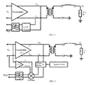
- a difficulty with this technique is that the load impedance Z L may vary, which may lead to an inaccurate power calculation.
- FIG. 2 shows a technique that can reduce the error caused by the change in the load impedance.
- the voltage at the transmitter output and the current of the transmitter are measured and multiplied to obtain an indication of output power.
- the current of the transmitter is measured by multiplying the transmitter input voltage with a replica of a transconductance cell.
- a phase shifter may account for the phase difference between the current and the voltage.
- the sensed current may not track the output current, which may lead to an inaccurate power measurement.
- FIGS. 3A and 3B show another technique in which an additional coil is added to a transformer to measure current, and output voltage is sensed capacitively. However, the measured voltage and current are not equal to the load current and voltage, which may lead to an inaccurate power measurement.
- power may be detected by measuring the load current and the load voltage from conductors coupled to the load.
- a selected phase adjustment may be introduced to correct the phase difference between the measured current and the measured voltage that may arise due to the load impedance.
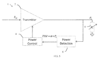
- FIG. 4 shows a transmitter system with power control loop 1 having a transmitter 2, a power control circuit 4, and a power detection circuit 6.
- Power detection circuit 6 detects the load power P L .
- the load may be an antenna and the power P L may be the power delivered to the antenna.
- the transmitter 2 may produce a signal having any suitable frequency above 0 Hz.
- the transmitter 2 may produce a signal having a frequency between 300 kHz and 300 GHz, however, the techniques described herein are not limited as to particular frequencies.
- the power detection circuit 6 may produce a TSSI (Transmitter Signal Strength Indication) that is proportional to P L .
- the power control circuit 4 controls the transmitter 2 based upon the TSSI signal. Accurate power detection by the power detection circuit 6 is important for appropriate control of the transmitter 2.
- FIG. 5 illustrates a challenge with detecting the load power. If the load impedance Z L is variable, the gain or attenuation between load power and detected power changes as Z L changes.
- FIG. 6 illustrates that in some embodiments, the transmitter system with power control loop 1 may include a switching power amplifier 2A.
- the switching power amplifier 2A may be any suitable type of amplifier, including class D, E, and F power amplifiers, and digital power amplifiers.
- the power produced by switching power amplifier 2A may be controlled using any suitable control technique, such as pulse-width modulation, for example.
- the switching power amplifier 2A may be controlled by power control circuit 4 based upon the TSSI signal. Since the switching power amplifier 2A is non-linear, it can be more effective to measure the power at the load rather than the input or output of the power amplifier 2A.
- FIG. 6 also shows that passive components 7 may be included between the output of the switching power amplifier 2A and the load. In some embodiments, the passive components 7 may tune out undesired harmonics. In some embodiments, passive components 7 may include an impedance matching network.
- FIG. 7 shows that in some embodiments, the transmitter system with power control loop 1 may include a power amplifier 2B having a plurality of power amplifier circuits.
- the power from the plurality of power amplifier circuits may be combined and delivered to a load.
- Examples of such amplifiers include Doherty power amplifiers, outphasing power amplifiers and digital power amplifiers,
- Power control circuit 4 may control the power amplifier circuits based on the TSSI signal. Individual power amplifier circuits may be controlled to produce the same amount of power or different amounts of power. As with the circuit of FIG. 6 , it can be more effective to measure the power at the load rather than the input or output of the power amplifier 2B.
- FIG. 8A illustrates a technique for detecting load power, according to some embodiments.
- a drive circuit 82 such as a power amplifier, for example, drives a load 84 having an impedance Z L with a current I L , a voltage V L and power P L .
- Load current I L may be measured by using a current sensor 86.
- Load voltage V L may be measured by using a voltage sensor 88.
- the inventors have recognized and appreciated that the magnitudes and phases of the measured current signal S I and the measured voltage signal S V0 may vary as the load impedance Z L varies. Variation in the load impedance changes the voltage standing wave ratio (VSWR), which can produce different magnitudes and phases in the voltage and current measurements.
- VSWR voltage standing wave ratio
- a phase delay ⁇ may be added to the measured voltage signal S V0 by a phase delay unit 90.
- the phase delayed voltage signal S V is multiplied by the measured current S I by a multiplier 92.
- the multiplied value may be low pass filtered by a low pass filter or averaging unit 94 to produce a determined load power P DET .
- the techniques described herein are not limited to adding a phase delay to the signal measured by the voltage sensor 88, as in some embodiments a phase delay may be added to the signal measured by the current sensor 86, or different phase delays may be added to both the current and voltage measurements to achieve the same result.
- phase delay ⁇ may accurately compensate for the variation in load impedance, which can produce an accurate power measurement.
- the power detector is capable of RMS power detection, sinusoidal waves are used to demonstrate the concept in the following analysis for simplicity.
- V ⁇ L V m Z
- the generated product is filtered by an averaging unit or low pass filter (LPF) 94:
- phase delay ⁇ that is appropriate for a particular implementation may be selected by calibration, modeling and/or simulation.
- the phase delay ⁇ is tunable, which allows compensating for variations in temperature and frequency as well as processing variations.
- one or more attenuators and/or amplifiers may be included in the signal path(s) before or after the sensor(s), which may extend the dynamic range of the power detector.
- Such attenuator(s) and/or amplifier(s) may be considered part of the current sensor 86 and/or the voltage sensor 88. This is illustrated in FIG. 8A as a gain A I of the current sensor 86 and a gain A v of the voltage sensor 88.
- the gain A I and/or the gain A v may have a value less than one to attenuate a detected signal, equal to one to produce no attenuation or amplification, or greater than one to amplify a detected signal.
- the attenuators and/or amplifiers may be implemented in analog and/or digital circuitry.
- the gain A I and/or the gain A v may be variable.
- the one or more attenuators and/or amplifiers may be tunable to produce selected gain(s) in the current and/or voltage sense path.
- FIG. 8B shows an embodiment in which the phase delay ⁇ is tunable and may be calibrated.
- FIG. 8B shows a phase shift controller 96 may be included in power detection circuit 6 that can control the phase delay ⁇ .
- the phase shift controller 96 may calibrate the phase delay ⁇ based on a programmed calibration sequence.
- Phase shift controller 96 and power control circuit 4 may be implemented by the same controller (e.g., a microprocessor or control circuit) or different controllers.
- FIG. 8C shows an embodiment for detecting load power, according to some embodiments, in which a phase delay unit 90 is present in the current sensing path.
- the phase delay may be tunable and/or may be calibrated, as discussed above.
- phase delays may be introduced in both the current sensing path and the voltage sensing path.
- FIG. 8D shows an embodiment in which a phase delay may be introduced in the voltage and/or current sensing path in the voltage and/or current sensors.
- a phase delay ⁇ v may be introduced in the signal measured by the voltage sensor 86
- a phase delay ⁇ I may be introduced in the signal measured by the current sensor 88
- both phase delays ⁇ v and ⁇ I may be introduced.
- Phase delays ⁇ v and ⁇ I may be introduced digitally or using analog components.
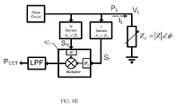
- FIG. 8E shows an embodiment in which a phase delay may be introduced in the voltage and/or current sensing path in a multiplier 92, which may be a circuit and/or software.
- a phase delay ⁇ v may be introduced to S V
- a phase delay ⁇ I may be introduced to S I
- both phase delays ⁇ v and ⁇ I may be introduced.
- one or more phase delays may be introduced anywhere in the voltage and/or current sensing paths.
- the voltage sensor 88 may include a conductor or other circuit element coupled to the load.
- the conductor of the voltage sensor 88 may be a bondwire, trace, solder ball, via, coupled line or and/or any other suitable conductor.
- the current sensor 86 may be a conductor that is positioned to inductively sense the load current from a conductor that provides the load current to the load.
- the conductor of the current sensor 86 may be a bondwire, trace, solder ball, via, coupled line or and/or any other suitable conductor.
- the phase delay unit 90, multiplier 92 and low pass filter and/or averaging unit 94 may be implemented using analog or digital component(s).
- the phase delay unit 90 may be an analog circuit element that delays a signal.
- the phase delay unit 90 may be implemented digitally using a digital delay element or by converting S V0 and/or S I to digital values and digitally delaying one or both signals.
- phase delay unit 90 may produce a delay ⁇ that is tunable. If phase delay unit 90 is implemented digitally, the phase delay unit 90 may be controlled to change the delay using a programmable delay line, software or firmware, for example.
- multiplier 92 may be implemented using an analog circuit or digitally using digital components and/or software or firmware.
- the low pass filter and/or averaging unit 94 may be implemented using an analog circuit, a digital circuit, or in software or firmware.
- the low pass filter and/or averaging unit 94 need not be a "filter” per se, as it may implement any suitable time-averaging technique.
- FIG. 9 shows an embodiment in which a conductor L0 connects the drive circuit 82 to the load 84.
- a second conductor L1 is coupled to the load 84 to make a voltage measurement S V0 that is provided to the phase delay unit 90.
- Conductor L1 is an example of a voltage sensor 88.
- Phase delay unit 90 may be a circuit that presents a high impedance to L1, thus the current I L 1 flowing through L1 is zero, so S V 0 is a faithful copy of V L .
- a third conductor L2, coupled between the multiplier 92 and ground, is positioned proximate the conductor L0, and due to inductive coupling, a current through conductor L0 induces a current in conductor L2, which is provided as a measurement S I of the load current I L .
- the conductors L0, L1 may be bondwires.
- the techniques described herein are not limited in this respect, as any suitable conductors may be used such as solder balls, vias, traces, or coupled lines, by way of example and not limitation.
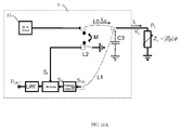
- FIG. 10A-D address possible implementation issues related to parasitics, especially for high frequency applications.
- L0 and L2 are assumed to be inductors.
- the sensed current S I deviates from I L because of current flowing through the parasitic capacitor C3.
- the effect of the parasitic capacitor C3 can be compensated as shown in FIG. 10B .
- an inductor L3 is coupled between the ground and the output node coupled to the load, having an inductance selected to resonate with C3 at the operating frequency, which cancels the current through C3. Accordingly, S I will be a faithful copy of I L .
- FIG. 10C shows an example in which S V0 is measured from the output of the drive circuit 82. Due to the current flowing through L0, which has an inductance, S V0 deviates from V L . As shown in FIG. 10D , a capacitor C0 can be inserted coupled between L0 and the drive circuit 82, with a capacitance selected to resonate with L0 at the operating frequency. Thus, S V0 is a faithful copy of V L .
- FIG. 10E shows a differential implementation of a power detector that can detect power from a drive circuit 82 that is differentially connected to a load 84.
- Conductors L3 and L0 couple the positive and negative output terminals of the drive circuit 82 to the positive and negative terminals of the load 84, respectively.
- Conductors L5 and L1 are coupled to the load 84 to make a voltage measurement at the positive and negative terminals of the load 84, respectively.
- the voltage measurements from conductors L5 and L1 are provided to phase delay unit 90, which delays the differential voltage measurement and provides it to multiplier 92.
- Conductors L4 and L2 are inductively coupled to conductors L3 and L0, respectively, and produce current measurements that are provided to multiplier 92.
- Multiplier 92 multiplies the differential current measurement and delayed voltage measurement.
- the phase delay may be introduced in the current sensing path, or in both the voltage sensing path and current sensing path.
- both current and voltage are measured differentially.
- the techniques described herein are not limited to measuring both current and voltage differentially, as a combination of a single-ended measurement and differential measurement may be used. For example, voltage may be measured differentially and current may be measured using a single-ended configuration, or current may be measured differentially and voltage may be measured using a single-ended configuration.
- FIGS. 11A and 11B show ways to implement the above-described techniques with different packages.
- FIG. 11A shows a way to implement the power sensing technique in a SOC (system on chip) with a QFN (Quad flat no-lead) package.
- a bondwire L0 is used to couple the output of the drive circuit 82 to the QFN load pin.
- a separate bondwire L1 is arranged to sense the load voltage, coupled to the phase delay unit 90.
- An additional bondwire L2, coupled to the QFN ground terminal, is placed proximate L0 to sense the load current.
- the power sensing scheme can be implemented in CSP (chip-scale package) type package. The current sensing can be accomplished with magnetic couplings between either the vias (k1) or the coupled lines (k2). Solder balls are shown as connecting the die, substrate and PCB.
- controller 96 and/or power control circuit 4 may be implemented using hardware or a combination of hardware and software.
- suitable software code can be executed on any suitable processor (e.g., a microprocessor) or collection of processors.
- the one or more controllers can be implemented in numerous ways, such as with dedicated hardware, or with general purpose hardware (e.g., one or more processors) that is programmed using microcode or software to perform the functions recited above.
Landscapes
- Engineering & Computer Science (AREA)
- Power Engineering (AREA)
- Physics & Mathematics (AREA)
- General Physics & Mathematics (AREA)
- Measurement Of Current Or Voltage (AREA)
- Measuring Instrument Details And Bridges, And Automatic Balancing Devices (AREA)
- Amplifiers (AREA)
Abstract
Description
- The techniques described herein relate to accurately detecting power delivered to a load, such as the power delivered to an antenna by a power amplifier.
- In radio frequency (RF) communications, a radio signal is transmitted by driving an antenna using a power amplifier. Various techniques have been proposed for measuring the power delivered to an antenna, however, they suffer from limitations that affect the accuracy of the power measurement.
- Some embodiments relate to power detector including a voltage sensor configured to detect a voltage of a load and a current sensor configured to detect a current of the load. The power detector also includes circuitry configured to introduce a phase delay between the detected voltage of the load and the detected current of the load, thereby producing a voltage measurement and a current measurement. The circuitry is also configured to multiply the voltage measurement and the current measurement.
- The phase delay may be introduced in at least one of a voltage sensing path and a current sensing path.
- The phase delay may be introduced in at least one of the voltage sensor, the current sensor, a phase delay unit in a current path, a phase delay unit in a voltage path, and a phase delay element in a multiplier circuit.
- The voltage sensor may be a differential voltage sensor and/or the current sensor may be a differential current sensor.
- The phase delay may be introduced in at least one of the current sensor, the voltage sensor, a phase delay unit, and a multiplier.
- The circuitry may be configured to amplify and/or attenuate the detected voltage of the load and/or the detected current of the load.
- The circuitry may be configured to amplify and/or attenuate the detected voltage of the load and/or the detected current of the load by a tunable gain.
- Some embodiments relate to an apparatus comprising the power detector and a load connected to the power detector.
- Some embodiments relate to a power detection method. The method includes detecting a voltage of a load. The method also includes detecting a current of the load. The method additionally includes introducing a phase delay between the detected voltage of the load and the detected current of the load, thereby producing a voltage measurement and a current measurement. The method further includes multiplying the voltage measurement and the current measurement.
- The power detection method may further comprise calibrating the phase delay. The current of the load may be detected inductively.
- The method may further comprise low-pass filtering a product of the voltage measurement and the current measurement.
- The foregoing summary is provided by way of illustration and is not intended to be limiting.
- In the drawings, each identical or nearly identical component that is illustrated in various figures is represented by a like reference character. For purposes of clarity, not every component may be labeled in every drawing. The drawings are not necessarily drawn to scale, with emphasis instead being placed on illustrating various aspects of the techniques and devices described herein.
-
FIG. 1 shows a technique for detecting power that involves squaring the voltage at the output of a transmitter. -
FIG. 2 shows a technique in which the voltage at the transmitter output and the current of the transmitter are measured and multiplied to obtain an indication of output power. Specifically, the current of the transmitter is measured by multiplying the transmitter input voltage with a replica of the transconductance cell. -
FIGS. 3A and 3B show another technique in which an additional coil is added to a transformer to measure current, and output voltage is sensed capacitively, as described in F. Francois, P. Reynaert, "A transformer-Coupled True-RMS Power Detector in 40nm CMOS," ISSCC Dig. Tech. Papers, pp. 62-63, Feb.2014. -
FIG. 4 shows a transmitter system with power control loop having a transmitter , a power control circuit, and a power detection circuit, according to some embodiments. -
FIG. 5 illustrates a variable load impedance. -
FIG. 6 illustrates a switching power amplifier. -
FIG. 7 shows a power amplifier having a plurality of power amplifier circuits. -
FIG. 8A illustrates a technique for detecting load power, according to some embodiments, in which a phase delay unit is present in the voltage sensing path. -
FIG. 8B shows an embodiment with a controller for controlling and/or calibrating the phase delay. -
FIG. 8C illustrates a technique for detecting load power, according to some embodiments, in which a phase delay unit is present in the current sensing path. -
FIG. 8D shows an embodiment in which a phase delay may be introduced in the voltage and/or current sensing path in the voltage and/or current sensors. -
FIG. 8E shows an embodiment in which a phase delay may be introduced in the voltage and/or current sensing path in a multiplier. -
FIG. 8F shows variable gains AI and Av in the current sense path and the voltage sense path. -
FIG. 9 shows an embodiment in which the current and voltage sensors are conductors. -
FIGS. 10A-D show solutions to address to parasitics, especially for high frequency applications, according to some embodiments. -
FIG. 10E shows a differential implementation of a power detector that can detect power from a drive circuit that is differentially connected to a load -
FIGS. 11A and11B show ways to implement the techniques described herein with different packages. - As mentioned above, various techniques have been proposed for accurately measuring load power, but they suffer from limitations that affect their accuracy.
-
FIG. 1 shows a technique for detecting power that squares the voltage at the output of a transmitter, and calculates power based on Pout = V2 out / ZL. However, a difficulty with this technique is that the load impedance ZL may vary, which may lead to an inaccurate power calculation. -
FIG. 2 shows a technique that can reduce the error caused by the change in the load impedance. The voltage at the transmitter output and the current of the transmitter are measured and multiplied to obtain an indication of output power. Specifically, the current of the transmitter is measured by multiplying the transmitter input voltage with a replica of a transconductance cell. A phase shifter may account for the phase difference between the current and the voltage. However, the sensed current may not track the output current, which may lead to an inaccurate power measurement. -
FIGS. 3A and 3B show another technique in which an additional coil is added to a transformer to measure current, and output voltage is sensed capacitively. However, the measured voltage and current are not equal to the load current and voltage, which may lead to an inaccurate power measurement. - In some embodiments, power may be detected by measuring the load current and the load voltage from conductors coupled to the load. A selected phase adjustment may be introduced to correct the phase difference between the measured current and the measured voltage that may arise due to the load impedance.
-
FIG. 4 shows a transmitter system withpower control loop 1 having atransmitter 2, apower control circuit 4, and apower detection circuit 6.Power detection circuit 6 detects the load power PL. In some embodiments, the load may be an antenna and the power PL may be the power delivered to the antenna. However, the techniques described herein are not limited to detecting the power delivered to an antenna. Thetransmitter 2 may produce a signal having any suitable frequency above 0 Hz. In some embodiments, thetransmitter 2 may produce a signal having a frequency between 300 kHz and 300 GHz, however, the techniques described herein are not limited as to particular frequencies. Thepower detection circuit 6 may produce a TSSI (Transmitter Signal Strength Indication) that is proportional to PL. Thepower control circuit 4 controls thetransmitter 2 based upon the TSSI signal. Accurate power detection by thepower detection circuit 6 is important for appropriate control of thetransmitter 2. -
FIG. 5 illustrates a challenge with detecting the load power. If the load impedance ZL is variable, the gain or attenuation between load power and detected power changes as ZL changes. -
FIG. 6 illustrates that in some embodiments, the transmitter system withpower control loop 1 may include aswitching power amplifier 2A. The switchingpower amplifier 2A may be any suitable type of amplifier, including class D, E, and F power amplifiers, and digital power amplifiers. The power produced by switchingpower amplifier 2A may be controlled using any suitable control technique, such as pulse-width modulation, for example. In some embodiments, the switchingpower amplifier 2A may be controlled bypower control circuit 4 based upon the TSSI signal. Since the switchingpower amplifier 2A is non-linear, it can be more effective to measure the power at the load rather than the input or output of thepower amplifier 2A.FIG. 6 also shows thatpassive components 7 may be included between the output of the switchingpower amplifier 2A and the load. In some embodiments, thepassive components 7 may tune out undesired harmonics. In some embodiments,passive components 7 may include an impedance matching network. -
FIG. 7 shows that in some embodiments, the transmitter system withpower control loop 1 may include apower amplifier 2B having a plurality of power amplifier circuits. The power from the plurality of power amplifier circuits may be combined and delivered to a load. Examples of such amplifiers include Doherty power amplifiers, outphasing power amplifiers and digital power amplifiers,Power control circuit 4 may control the power amplifier circuits based on the TSSI signal. Individual power amplifier circuits may be controlled to produce the same amount of power or different amounts of power. As with the circuit ofFIG. 6 , it can be more effective to measure the power at the load rather than the input or output of thepower amplifier 2B. -
FIG. 8A illustrates a technique for detecting load power, according to some embodiments. In the embodiment ofFIG. 8A , adrive circuit 82 such as a power amplifier, for example, drives aload 84 having an impedance ZL with a current IL, a voltage VL and power PL. Load current IL may be measured by using acurrent sensor 86. Load voltage VL may be measured by using avoltage sensor 88. The inventors have recognized and appreciated that the magnitudes and phases of the measured current signal SI and the measured voltage signal SV0 may vary as the load impedance ZL varies. Variation in the load impedance changes the voltage standing wave ratio (VSWR), which can produce different magnitudes and phases in the voltage and current measurements. In some embodiments, a phase delay θ may be added to the measured voltage signal SV0 by aphase delay unit 90. The phase delayed voltage signal SV is multiplied by the measured current SI by amultiplier 92. The multiplied value may be low pass filtered by a low pass filter or averagingunit 94 to produce a determined load power PDET. However, the techniques described herein are not limited to adding a phase delay to the signal measured by thevoltage sensor 88, as in some embodiments a phase delay may be added to the signal measured by thecurrent sensor 86, or different phase delays may be added to both the current and voltage measurements to achieve the same result. - The inventors have recognized and appreciated that a properly selected phase delay θ may accurately compensate for the variation in load impedance, which can produce an accurate power measurement. Although the power detector is capable of RMS power detection, sinusoidal waves are used to demonstrate the concept in the following analysis for simplicity. Assuming a complex load ZL, with magnitude of |Z| and phase of φ, is presented to the
drive circuit 82, the load voltage VL and load current IL can be represented by the following equations, where Vm and Im are the magnitudes of the load voltage and the load current, respectively:


- In some embodiments, one or more attenuators and/or amplifiers may be included in the signal path(s) before or after the sensor(s), which may extend the dynamic range of the power detector. Such attenuator(s) and/or amplifier(s) may be considered part of the
current sensor 86 and/or thevoltage sensor 88. This is illustrated inFIG. 8A as a gain AI of thecurrent sensor 86 and a gain Av of thevoltage sensor 88. The gain AI and/or the gain Av may have a value less than one to attenuate a detected signal, equal to one to produce no attenuation or amplification, or greater than one to amplify a detected signal. The attenuators and/or amplifiers may be implemented in analog and/or digital circuitry. - As shown in
FIG. 8F , in some embodiments, the gain AI and/or the gain Av may be variable. For example, the one or more attenuators and/or amplifiers may be tunable to produce selected gain(s) in the current and/or voltage sense path. -
FIG. 8B shows an embodiment in which the phase delay θ is tunable and may be calibrated.FIG. 8B shows aphase shift controller 96 may be included inpower detection circuit 6 that can control the phase delay θ. In some embodiments, thephase shift controller 96 may calibrate the phase delay θ based on a programmed calibration sequence.Phase shift controller 96 andpower control circuit 4 may be implemented by the same controller (e.g., a microprocessor or control circuit) or different controllers. -
FIG. 8C shows an embodiment for detecting load power, according to some embodiments, in which aphase delay unit 90 is present in the current sensing path. In such embodiments, the phase delay may be tunable and/or may be calibrated, as discussed above. In some embodiments, phase delays may be introduced in both the current sensing path and the voltage sensing path. -
FIG. 8D shows an embodiment in which a phase delay may be introduced in the voltage and/or current sensing path in the voltage and/or current sensors. For example, a phase delay θ v may be introduced in the signal measured by thevoltage sensor 86, a phase delay θ I may be introduced in the signal measured by thecurrent sensor 88, or both phase delays θ v and θ I may be introduced. Phase delays θ v and θ I may be introduced digitally or using analog components. -
FIG. 8E shows an embodiment in which a phase delay may be introduced in the voltage and/or current sensing path in amultiplier 92, which may be a circuit and/or software. For example, a phase delay θ v may be introduced to SV, a phase delay θ I may be introduced to SI, or both phase delays θ v and θ I may be introduced. Thus, as seen from the above, one or more phase delays may be introduced anywhere in the voltage and/or current sensing paths. - Referring to
FIG. 8A , in some embodiments, thevoltage sensor 88 may include a conductor or other circuit element coupled to the load. For example, as discussed below, the conductor of thevoltage sensor 88 may be a bondwire, trace, solder ball, via, coupled line or and/or any other suitable conductor. - In some embodiments, the
current sensor 86 may be a conductor that is positioned to inductively sense the load current from a conductor that provides the load current to the load. For example, as discussed below, the conductor of thecurrent sensor 86 may be a bondwire, trace, solder ball, via, coupled line or and/or any other suitable conductor. - The
phase delay unit 90,multiplier 92 and low pass filter and/or averagingunit 94 may be implemented using analog or digital component(s). For example, thephase delay unit 90 may be an analog circuit element that delays a signal. As another example, thephase delay unit 90 may be implemented digitally using a digital delay element or by converting SV0 and/or SI to digital values and digitally delaying one or both signals. As discussed above,phase delay unit 90 may produce a delay θ that is tunable. Ifphase delay unit 90 is implemented digitally, thephase delay unit 90 may be controlled to change the delay using a programmable delay line, software or firmware, for example. Similarly,multiplier 92 may be implemented using an analog circuit or digitally using digital components and/or software or firmware. Also, the low pass filter and/or averagingunit 94 may be implemented using an analog circuit, a digital circuit, or in software or firmware. The low pass filter and/or averagingunit 94 need not be a "filter" per se, as it may implement any suitable time-averaging technique. -
FIG. 9 shows an embodiment in which a conductor L0 connects thedrive circuit 82 to theload 84. A second conductor L1 is coupled to theload 84 to make a voltage measurement SV0 that is provided to thephase delay unit 90. Conductor L1 is an example of avoltage sensor 88.Phase delay unit 90 may be a circuit that presents a high impedance to L1, thus the current I L1 flowing through L1 is zero, so S V0 is a faithful copy of VL. A third conductor L2, coupled between themultiplier 92 and ground, is positioned proximate the conductor L0, and due to inductive coupling, a current through conductor L0 induces a current in conductor L2, which is provided as a measurement SI of the load current IL. Thus, conductor L2 is an example of acurrent sensor 86. If L0 and L2 are inductors, SI will be a faithful copy of IL with close to a 90° phase shift if the multiplier input impedance is high. By inserting a θ=90° phase shift between L1 and themultiplier 92, PDET will be a faithful copy of PL , independent of the change of |Z| or φ. In some embodiments, the conductors L0, L1 may be bondwires. However, the techniques described herein are not limited in this respect, as any suitable conductors may be used such as solder balls, vias, traces, or coupled lines, by way of example and not limitation. -
FIG. 10A-D address possible implementation issues related to parasitics, especially for high frequency applications. For the sake of discussion, L0 and L2 are assumed to be inductors. InFIG. 10A , the sensed current SI deviates from IL because of current flowing through the parasitic capacitor C3. The effect of the parasitic capacitor C3 can be compensated as shown inFIG. 10B . InFIG. 10B , an inductor L3 is coupled between the ground and the output node coupled to the load, having an inductance selected to resonate with C3 at the operating frequency, which cancels the current through C3. Accordingly, SI will be a faithful copy of IL. -
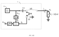
FIG. 10C shows an example in which SV0 is measured from the output of thedrive circuit 82. Due to the current flowing through L0, which has an inductance, SV0 deviates from VL. As shown inFIG. 10D , a capacitor C0 can be inserted coupled between L0 and thedrive circuit 82, with a capacitance selected to resonate with L0 at the operating frequency. Thus, SV0 is a faithful copy of VL. -
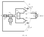
FIG. 10E shows a differential implementation of a power detector that can detect power from adrive circuit 82 that is differentially connected to aload 84. Conductors L3 and L0 couple the positive and negative output terminals of thedrive circuit 82 to the positive and negative terminals of theload 84, respectively. Conductors L5 and L1 are coupled to theload 84 to make a voltage measurement at the positive and negative terminals of theload 84, respectively. The voltage measurements from conductors L5 and L1 are provided to phasedelay unit 90, which delays the differential voltage measurement and provides it tomultiplier 92. Conductors L4 and L2 are inductively coupled to conductors L3 and L0, respectively, and produce current measurements that are provided tomultiplier 92.Multiplier 92 multiplies the differential current measurement and delayed voltage measurement. In some embodiments, and as discussed above, the phase delay may be introduced in the current sensing path, or in both the voltage sensing path and current sensing path. In the example ofFIG. 10E , both current and voltage are measured differentially. However, the techniques described herein are not limited to measuring both current and voltage differentially, as a combination of a single-ended measurement and differential measurement may be used. For example, voltage may be measured differentially and current may be measured using a single-ended configuration, or current may be measured differentially and voltage may be measured using a single-ended configuration. -
FIGS. 11A and11B show ways to implement the above-described techniques with different packages.FIG. 11A shows a way to implement the power sensing technique in a SOC (system on chip) with a QFN (Quad flat no-lead) package. A bondwire L0 is used to couple the output of thedrive circuit 82 to the QFN load pin. A separate bondwire L1 is arranged to sense the load voltage, coupled to thephase delay unit 90. An additional bondwire L2, coupled to the QFN ground terminal, is placed proximate L0 to sense the load current. Similarly, as shown inFIG. 11B , the power sensing scheme can be implemented in CSP (chip-scale package) type package. The current sensing can be accomplished with magnetic couplings between either the vias (k1) or the coupled lines (k2). Solder balls are shown as connecting the die, substrate and PCB. - In some embodiments,
controller 96 and/orpower control circuit 4 may be implemented using hardware or a combination of hardware and software. When implemented using software, suitable software code can be executed on any suitable processor (e.g., a microprocessor) or collection of processors. The one or more controllers can be implemented in numerous ways, such as with dedicated hardware, or with general purpose hardware (e.g., one or more processors) that is programmed using microcode or software to perform the functions recited above. - Various aspects of the apparatus and techniques described herein may be used alone, in combination, or in a variety of arrangements not specifically discussed in the embodiments described in the foregoing description and is therefore not limited in its application to the details and arrangement of components set forth in the foregoing description or illustrated in the drawings. For example, aspects described in one embodiment may be combined in any manner with aspects described in other embodiments.
- Use of ordinal terms such as "first," "second," "third," etc., in the claims to modify a claim element does not by itself connote any priority, precedence, or order of one claim element over another or the temporal order in which acts of a method are performed, but are used merely as labels to distinguish one claim element having a certain name from another element having a same name (but for use of the ordinal term) to distinguish the claim elements.
- Also, the phraseology and terminology used herein is for the purpose of description and should not be regarded as limiting. The use of "including," "comprising," or "having," "containing," "involving," and variations thereof herein, is meant to encompass the items listed thereafter and equivalents thereof as well as additional items.
Claims (15)
- A power detector, comprising:a voltage sensor configured to detect a voltage of a load;a current sensor configured to detect a current of the load; andcircuitry configured to:introduce a phase delay between the detected voltage of the load and the detected current of the load, thereby producing a voltage measurement and a current measurement; andmultiply the voltage measurement and the current measurement.
- The power detector of claim 1, wherein the voltage sensor or the current sensor comprises a conductor or a circuit element.
- The power detector of claim 2, wherein the voltage sensor or the current sensor comprises a conductor, and the conductor comprises at least one of a bondwire, a coupled line, a via and a solder ball.
- The power detector of any preceding claim, wherein the current sensor comprises a conductor positioned to inductively sense the current of the load.
- The power detector of any preceding claim, wherein the phase delay is tunable.
- The power detector of any preceding claim, wherein the phase delay is calibrated to account for processing variations, variations in temperature and/or variations in frequency.
- The power detector of any preceding claim, further comprising a low pass filter and/or averaging unit to filter and/or average a product of the current measurement and the voltage measurement.
- The power detector of any preceding claim, implemented in a quad flat-lead package or chip scale package.
- The power detector of any preceding claim, wherein the load is driven by an amplifier, and optionally the amplifier comprises a switching amplifier.
- The power detector of any preceding claim, wherein the amplifier comprises a plurality of amplifier circuits that combine their outputs to drive the load.
- The power detector of any preceding claim, wherein the load comprises an antenna.
- The power detector of any preceding claim, further comprising a circuit element to resonate with a parasitic inductance or capacitance at a frequency of operation of the load.
- The power detector of claim 12, wherein the circuit element comprises an inductive element that resonates with a parasitic capacitance, the parasitic capacitance being in parallel with the load.
- The power detector of claim 12, wherein the circuit element comprises a capacitive element that resonates with a parasitic inductance, the parasitic inductance being in series with the load.
- A power detection method, comprising,
detecting a voltage of a load;
detecting a current of the load;
introducing a phase delay between the detected voltage of the load and the detected current of the load, thereby producing a voltage measurement and a current measurement; and
multiplying the voltage measurement and the current measurement.
Applications Claiming Priority (2)
| Application Number | Priority Date | Filing Date | Title |
|---|---|---|---|
| US201562160807P | 2015-05-13 | 2015-05-13 | |
| US14/963,921 US10082528B2 (en) | 2015-05-13 | 2015-12-09 | Power detector |
Publications (2)
| Publication Number | Publication Date |
|---|---|
| EP3101435A1 true EP3101435A1 (en) | 2016-12-07 |
| EP3101435B1 EP3101435B1 (en) | 2020-10-28 |
Family
ID=55968999
Family Applications (1)
| Application Number | Title | Priority Date | Filing Date |
|---|---|---|---|
| EP16169467.4A Active EP3101435B1 (en) | 2015-05-13 | 2016-05-12 | Power detection |
Country Status (3)
| Country | Link |
|---|---|
| US (1) | US10082528B2 (en) |
| EP (1) | EP3101435B1 (en) |
| CN (1) | CN106154029B (en) |
Families Citing this family (4)
| Publication number | Priority date | Publication date | Assignee | Title |
|---|---|---|---|---|
| TWI768926B (en) * | 2021-05-25 | 2022-06-21 | 瑞昱半導體股份有限公司 | Transmit-signal strength indicator circuit and transmitting circuit |
| CN115412186B (en) * | 2021-05-27 | 2025-07-08 | 瑞昱半导体股份有限公司 | Signal strength indicator circuit and transmission circuit |
| CN116400136B (en) * | 2023-03-24 | 2023-10-20 | 浙江伊控动力系统有限公司 | Method for calculating phase shift of current sensor |
| EP4567435A1 (en) | 2023-12-06 | 2025-06-11 | Nxp B.V. | Power detector and method for operating a power detector |
Citations (4)
| Publication number | Priority date | Publication date | Assignee | Title |
|---|---|---|---|---|
| US5017860A (en) * | 1988-12-02 | 1991-05-21 | General Electric Company | Electronic meter digital phase compensation |
| EP1235075A2 (en) * | 2001-02-16 | 2002-08-28 | Z. BAVELLONI S.p.A. | Power measurement device for motors |
| US20100201346A1 (en) * | 2009-02-06 | 2010-08-12 | Zhong You | Rf power detector |
| US20110273164A1 (en) * | 2010-05-05 | 2011-11-10 | Dupuis Timothy J | Delivered power detection for power amplifiers and related systems and methods |
Family Cites Families (20)
| Publication number | Priority date | Publication date | Assignee | Title |
|---|---|---|---|---|
| US4126860A (en) * | 1970-02-06 | 1978-11-21 | Gte Sylvania Incorporated | Wire detector |
| US5604507A (en) * | 1996-02-28 | 1997-02-18 | Antenex, Inc. | Wide-banded mobile antenna |
| US6205171B1 (en) * | 1998-05-08 | 2001-03-20 | Industrial Technology Research Institute | Antenna selector switch |
| EP1301960A1 (en) * | 2000-07-20 | 2003-04-16 | Paratek Microwave, Inc. | Tunable microwave devices with auto-adjusting matching circuit |
| US7865154B2 (en) * | 2000-07-20 | 2011-01-04 | Paratek Microwave, Inc. | Tunable microwave devices with auto-adjusting matching circuit |
| US6791302B2 (en) * | 2001-03-21 | 2004-09-14 | Primarion, Inc. | Methods and apparatus for open-loop enhanced control of power supply transients |
| EP1819038A4 (en) * | 2004-11-30 | 2008-07-09 | Fujitsu Ltd | SIGNAL EXTRACTION CIRCUIT AND DISTORTION AMPLIFIER THEREFOR |
| US20060176046A1 (en) * | 2005-02-07 | 2006-08-10 | Walker Jason A | Power meter for biasing an audio amplifier |
| US7937106B2 (en) * | 2006-04-24 | 2011-05-03 | ParkerVision, Inc, | Systems and methods of RF power transmission, modulation, and amplification, including architectural embodiments of same |
| US7894546B2 (en) * | 2006-08-04 | 2011-02-22 | Axiom Microdevices, Inc. | Replica linearized power amplifier |
| US7852150B1 (en) * | 2007-12-20 | 2010-12-14 | The Tc Group A/S | Switching amplifier driven by a controlled power supply |
| US8339208B2 (en) * | 2010-06-08 | 2012-12-25 | The Hong Kong University Of Science And Technology | Method and apparatus for tuning frequency of LC-oscillators based on phase-tuning technique |
| JP5300028B2 (en) * | 2010-12-28 | 2013-09-25 | オリジン電気株式会社 | Single-phase voltage type AC / DC converter and system interconnection system |
| JP5729693B2 (en) * | 2011-03-30 | 2015-06-03 | 株式会社ダイヘン | High frequency power supply |
| JP5751324B2 (en) * | 2011-05-30 | 2015-07-22 | 日本電気株式会社 | VSWR measurement circuit, wireless communication apparatus, VSWR measurement method, and VSWR measurement program |
| US9128125B2 (en) * | 2012-06-14 | 2015-09-08 | Micrel, Inc. | Current sensing using a metal-on-passivation layer on an integrated circuit die |
| US9356447B2 (en) * | 2012-07-24 | 2016-05-31 | International Business Machines Corporation | Predictive phase balancing for demand response |
| US8593219B1 (en) * | 2012-08-31 | 2013-11-26 | Motorola Solutions, Inc. | Method and apparatus for amplifying a radio frequency signal |
| US9312820B2 (en) * | 2012-09-23 | 2016-04-12 | Dsp Group Ltd. | CMOS based TX/RX switch |
| US9776071B2 (en) * | 2013-05-09 | 2017-10-03 | Mattel, Inc. | Resonant coils for use with games and toys |
-
2015
- 2015-12-09 US US14/963,921 patent/US10082528B2/en active Active
-
2016
- 2016-02-23 CN CN201610098410.3A patent/CN106154029B/en active Active
- 2016-05-12 EP EP16169467.4A patent/EP3101435B1/en active Active
Patent Citations (4)
| Publication number | Priority date | Publication date | Assignee | Title |
|---|---|---|---|---|
| US5017860A (en) * | 1988-12-02 | 1991-05-21 | General Electric Company | Electronic meter digital phase compensation |
| EP1235075A2 (en) * | 2001-02-16 | 2002-08-28 | Z. BAVELLONI S.p.A. | Power measurement device for motors |
| US20100201346A1 (en) * | 2009-02-06 | 2010-08-12 | Zhong You | Rf power detector |
| US20110273164A1 (en) * | 2010-05-05 | 2011-11-10 | Dupuis Timothy J | Delivered power detection for power amplifiers and related systems and methods |
Non-Patent Citations (1)
| Title |
|---|
| F. FRANCOIS; P. REYNAERT: "A transformer-Coupled True-RMS Power Detector in 40nm CMOS", ISSCC DIG. TECH. PAPERS, February 2014 (2014-02-01), pages 62 - 63, XP032575007, DOI: doi:10.1109/ISSCC.2014.6757338 |
Also Published As
| Publication number | Publication date |
|---|---|
| EP3101435B1 (en) | 2020-10-28 |
| US20160334444A1 (en) | 2016-11-17 |
| US10082528B2 (en) | 2018-09-25 |
| CN106154029B (en) | 2019-03-08 |
| CN106154029A (en) | 2016-11-23 |
Similar Documents
| Publication | Publication Date | Title |
|---|---|---|
| EP1800410B1 (en) | Impedance detector | |
| US9947985B2 (en) | System and method for a directional coupler | |
| US20040070453A1 (en) | Absolute power detector | |
| US20150199543A1 (en) | Method and apparatus for detecting an output power of a radio frequency transmitter | |
| EP3101435B1 (en) | Power detection | |
| US7821273B2 (en) | Circuit for detecting the impedance of a load | |
| CN206725656U (en) | LCR RF impedance testers | |
| TWI603578B (en) | Integrated technique for enhanced power amplifier forward power detection | |
| US6822433B1 (en) | Gain and phase detector having dual logarithmic amplifiers | |
| US6289205B1 (en) | Transmitter for communication devices | |
| CN104535838B (en) | Phase-frequency characteristic detector and method for detecting phase-frequency characteristic | |
| CN113533845A (en) | On-chip radio frequency power meter, chip, radio device and electronic equipment | |
| US20100201346A1 (en) | Rf power detector | |
| US5732332A (en) | Transmitter having temperature-compensated detector | |
| US9933464B2 (en) | Power detector | |
| CN104660186B (en) | A kind of match circuit determines method and load balance factor system | |
| JP2009177240A (en) | Semiconductor integrated circuit and characteristic calibration circuit provided therein | |
| CN101346031A (en) | Matcher and method for realizing matching control thereof | |
| US8717104B1 (en) | Vector voltage samplers for RF interface control of power amplifier | |
| Gecan et al. | Investigation of the practical output load impedance sensitivity of a 10 W GaN device subject to gate bias variation | |
| CN107800445B (en) | Transmitter, integrated circuit, detection unit, and method for testing integrated circuit | |
| KR102334597B1 (en) | Impedance monitoring apparatus and operating method thereof | |
| EP0444816A2 (en) | Circuit element measuring method and apparatus | |
| da Mota et al. | A true power detector for RF PA built-in calibration and testing | |
| CN107632197A (en) | A radio frequency power meter and equipment |
Legal Events
| Date | Code | Title | Description |
|---|---|---|---|
| PUAI | Public reference made under article 153(3) epc to a published international application that has entered the european phase |
Free format text: ORIGINAL CODE: 0009012 |
|
| STAA | Information on the status of an ep patent application or granted ep patent |
Free format text: STATUS: THE APPLICATION HAS BEEN PUBLISHED |
|
| AK | Designated contracting states |
Kind code of ref document: A1 Designated state(s): AL AT BE BG CH CY CZ DE DK EE ES FI FR GB GR HR HU IE IS IT LI LT LU LV MC MK MT NL NO PL PT RO RS SE SI SK SM TR |
|
| AX | Request for extension of the european patent |
Extension state: BA ME |
|
| STAA | Information on the status of an ep patent application or granted ep patent |
Free format text: STATUS: REQUEST FOR EXAMINATION WAS MADE |
|
| 17P | Request for examination filed |
Effective date: 20170607 |
|
| RBV | Designated contracting states (corrected) |
Designated state(s): AL AT BE BG CH CY CZ DE DK EE ES FI FR GB GR HR HU IE IS IT LI LT LU LV MC MK MT NL NO PL PT RO RS SE SI SK SM TR |
|
| STAA | Information on the status of an ep patent application or granted ep patent |
Free format text: STATUS: EXAMINATION IS IN PROGRESS |
|
| 17Q | First examination report despatched |
Effective date: 20190520 |
|
| GRAP | Despatch of communication of intention to grant a patent |
Free format text: ORIGINAL CODE: EPIDOSNIGR1 |
|
| STAA | Information on the status of an ep patent application or granted ep patent |
Free format text: STATUS: GRANT OF PATENT IS INTENDED |
|
| INTG | Intention to grant announced |
Effective date: 20200703 |
|
| GRAS | Grant fee paid |
Free format text: ORIGINAL CODE: EPIDOSNIGR3 |
|
| GRAA | (expected) grant |
Free format text: ORIGINAL CODE: 0009210 |
|
| STAA | Information on the status of an ep patent application or granted ep patent |
Free format text: STATUS: THE PATENT HAS BEEN GRANTED |
|
| AK | Designated contracting states |
Kind code of ref document: B1 Designated state(s): AL AT BE BG CH CY CZ DE DK EE ES FI FR GB GR HR HU IE IS IT LI LT LU LV MC MK MT NL NO PL PT RO RS SE SI SK SM TR |
|
| REG | Reference to a national code |
Ref country code: GB Ref legal event code: FG4D |
|
| REG | Reference to a national code |
Ref country code: CH Ref legal event code: EP |
|
| REG | Reference to a national code |
Ref country code: AT Ref legal event code: REF Ref document number: 1328736 Country of ref document: AT Kind code of ref document: T Effective date: 20201115 |
|
| REG | Reference to a national code |
Ref country code: DE Ref legal event code: R096 Ref document number: 602016046572 Country of ref document: DE |
|
| REG | Reference to a national code |
Ref country code: IE Ref legal event code: FG4D |
|
| REG | Reference to a national code |
Ref country code: AT Ref legal event code: MK05 Ref document number: 1328736 Country of ref document: AT Kind code of ref document: T Effective date: 20201028 |
|
| REG | Reference to a national code |
Ref country code: NL Ref legal event code: MP Effective date: 20201028 |
|
| PG25 | Lapsed in a contracting state [announced via postgrant information from national office to epo] |
Ref country code: GR Free format text: LAPSE BECAUSE OF FAILURE TO SUBMIT A TRANSLATION OF THE DESCRIPTION OR TO PAY THE FEE WITHIN THE PRESCRIBED TIME-LIMIT Effective date: 20210129 Ref country code: FI Free format text: LAPSE BECAUSE OF FAILURE TO SUBMIT A TRANSLATION OF THE DESCRIPTION OR TO PAY THE FEE WITHIN THE PRESCRIBED TIME-LIMIT Effective date: 20201028 Ref country code: NL Free format text: LAPSE BECAUSE OF FAILURE TO SUBMIT A TRANSLATION OF THE DESCRIPTION OR TO PAY THE FEE WITHIN THE PRESCRIBED TIME-LIMIT Effective date: 20201028 Ref country code: NO Free format text: LAPSE BECAUSE OF FAILURE TO SUBMIT A TRANSLATION OF THE DESCRIPTION OR TO PAY THE FEE WITHIN THE PRESCRIBED TIME-LIMIT Effective date: 20210128 Ref country code: PT Free format text: LAPSE BECAUSE OF FAILURE TO SUBMIT A TRANSLATION OF THE DESCRIPTION OR TO PAY THE FEE WITHIN THE PRESCRIBED TIME-LIMIT Effective date: 20210301 Ref country code: RS Free format text: LAPSE BECAUSE OF FAILURE TO SUBMIT A TRANSLATION OF THE DESCRIPTION OR TO PAY THE FEE WITHIN THE PRESCRIBED TIME-LIMIT Effective date: 20201028 |
|
| REG | Reference to a national code |
Ref country code: LT Ref legal event code: MG4D |
|
| PG25 | Lapsed in a contracting state [announced via postgrant information from national office to epo] |
Ref country code: ES Free format text: LAPSE BECAUSE OF FAILURE TO SUBMIT A TRANSLATION OF THE DESCRIPTION OR TO PAY THE FEE WITHIN THE PRESCRIBED TIME-LIMIT Effective date: 20201028 Ref country code: AT Free format text: LAPSE BECAUSE OF FAILURE TO SUBMIT A TRANSLATION OF THE DESCRIPTION OR TO PAY THE FEE WITHIN THE PRESCRIBED TIME-LIMIT Effective date: 20201028 Ref country code: SE Free format text: LAPSE BECAUSE OF FAILURE TO SUBMIT A TRANSLATION OF THE DESCRIPTION OR TO PAY THE FEE WITHIN THE PRESCRIBED TIME-LIMIT Effective date: 20201028 Ref country code: IS Free format text: LAPSE BECAUSE OF FAILURE TO SUBMIT A TRANSLATION OF THE DESCRIPTION OR TO PAY THE FEE WITHIN THE PRESCRIBED TIME-LIMIT Effective date: 20210228 Ref country code: PL Free format text: LAPSE BECAUSE OF FAILURE TO SUBMIT A TRANSLATION OF THE DESCRIPTION OR TO PAY THE FEE WITHIN THE PRESCRIBED TIME-LIMIT Effective date: 20201028 Ref country code: LV Free format text: LAPSE BECAUSE OF FAILURE TO SUBMIT A TRANSLATION OF THE DESCRIPTION OR TO PAY THE FEE WITHIN THE PRESCRIBED TIME-LIMIT Effective date: 20201028 Ref country code: BG Free format text: LAPSE BECAUSE OF FAILURE TO SUBMIT A TRANSLATION OF THE DESCRIPTION OR TO PAY THE FEE WITHIN THE PRESCRIBED TIME-LIMIT Effective date: 20210128 |
|
| PG25 | Lapsed in a contracting state [announced via postgrant information from national office to epo] |
Ref country code: HR Free format text: LAPSE BECAUSE OF FAILURE TO SUBMIT A TRANSLATION OF THE DESCRIPTION OR TO PAY THE FEE WITHIN THE PRESCRIBED TIME-LIMIT Effective date: 20201028 |
|
| REG | Reference to a national code |
Ref country code: DE Ref legal event code: R097 Ref document number: 602016046572 Country of ref document: DE |
|
| PG25 | Lapsed in a contracting state [announced via postgrant information from national office to epo] |
Ref country code: SK Free format text: LAPSE BECAUSE OF FAILURE TO SUBMIT A TRANSLATION OF THE DESCRIPTION OR TO PAY THE FEE WITHIN THE PRESCRIBED TIME-LIMIT Effective date: 20201028 Ref country code: RO Free format text: LAPSE BECAUSE OF FAILURE TO SUBMIT A TRANSLATION OF THE DESCRIPTION OR TO PAY THE FEE WITHIN THE PRESCRIBED TIME-LIMIT Effective date: 20201028 Ref country code: SM Free format text: LAPSE BECAUSE OF FAILURE TO SUBMIT A TRANSLATION OF THE DESCRIPTION OR TO PAY THE FEE WITHIN THE PRESCRIBED TIME-LIMIT Effective date: 20201028 Ref country code: LT Free format text: LAPSE BECAUSE OF FAILURE TO SUBMIT A TRANSLATION OF THE DESCRIPTION OR TO PAY THE FEE WITHIN THE PRESCRIBED TIME-LIMIT Effective date: 20201028 Ref country code: EE Free format text: LAPSE BECAUSE OF FAILURE TO SUBMIT A TRANSLATION OF THE DESCRIPTION OR TO PAY THE FEE WITHIN THE PRESCRIBED TIME-LIMIT Effective date: 20201028 Ref country code: CZ Free format text: LAPSE BECAUSE OF FAILURE TO SUBMIT A TRANSLATION OF THE DESCRIPTION OR TO PAY THE FEE WITHIN THE PRESCRIBED TIME-LIMIT Effective date: 20201028 |
|
| PG25 | Lapsed in a contracting state [announced via postgrant information from national office to epo] |
Ref country code: DK Free format text: LAPSE BECAUSE OF FAILURE TO SUBMIT A TRANSLATION OF THE DESCRIPTION OR TO PAY THE FEE WITHIN THE PRESCRIBED TIME-LIMIT Effective date: 20201028 |
|
| PLBE | No opposition filed within time limit |
Free format text: ORIGINAL CODE: 0009261 |
|
| STAA | Information on the status of an ep patent application or granted ep patent |
Free format text: STATUS: NO OPPOSITION FILED WITHIN TIME LIMIT |
|
| 26N | No opposition filed |
Effective date: 20210729 |
|
| PG25 | Lapsed in a contracting state [announced via postgrant information from national office to epo] |
Ref country code: AL Free format text: LAPSE BECAUSE OF FAILURE TO SUBMIT A TRANSLATION OF THE DESCRIPTION OR TO PAY THE FEE WITHIN THE PRESCRIBED TIME-LIMIT Effective date: 20201028 Ref country code: IT Free format text: LAPSE BECAUSE OF FAILURE TO SUBMIT A TRANSLATION OF THE DESCRIPTION OR TO PAY THE FEE WITHIN THE PRESCRIBED TIME-LIMIT Effective date: 20201028 |
|
| PG25 | Lapsed in a contracting state [announced via postgrant information from national office to epo] |
Ref country code: SI Free format text: LAPSE BECAUSE OF FAILURE TO SUBMIT A TRANSLATION OF THE DESCRIPTION OR TO PAY THE FEE WITHIN THE PRESCRIBED TIME-LIMIT Effective date: 20201028 |
|
| REG | Reference to a national code |
Ref country code: CH Ref legal event code: PL |
|
| PG25 | Lapsed in a contracting state [announced via postgrant information from national office to epo] |
Ref country code: MC Free format text: LAPSE BECAUSE OF FAILURE TO SUBMIT A TRANSLATION OF THE DESCRIPTION OR TO PAY THE FEE WITHIN THE PRESCRIBED TIME-LIMIT Effective date: 20201028 Ref country code: LU Free format text: LAPSE BECAUSE OF NON-PAYMENT OF DUE FEES Effective date: 20210512 Ref country code: LI Free format text: LAPSE BECAUSE OF NON-PAYMENT OF DUE FEES Effective date: 20210531 Ref country code: CH Free format text: LAPSE BECAUSE OF NON-PAYMENT OF DUE FEES Effective date: 20210531 |
|
| REG | Reference to a national code |
Ref country code: BE Ref legal event code: MM Effective date: 20210531 |
|
| PG25 | Lapsed in a contracting state [announced via postgrant information from national office to epo] |
Ref country code: IE Free format text: LAPSE BECAUSE OF NON-PAYMENT OF DUE FEES Effective date: 20210512 |
|
| PG25 | Lapsed in a contracting state [announced via postgrant information from national office to epo] |
Ref country code: IS Free format text: LAPSE BECAUSE OF FAILURE TO SUBMIT A TRANSLATION OF THE DESCRIPTION OR TO PAY THE FEE WITHIN THE PRESCRIBED TIME-LIMIT Effective date: 20210228 |
|
| PG25 | Lapsed in a contracting state [announced via postgrant information from national office to epo] |
Ref country code: BE Free format text: LAPSE BECAUSE OF NON-PAYMENT OF DUE FEES Effective date: 20210531 |
|
| PG25 | Lapsed in a contracting state [announced via postgrant information from national office to epo] |
Ref country code: HU Free format text: LAPSE BECAUSE OF FAILURE TO SUBMIT A TRANSLATION OF THE DESCRIPTION OR TO PAY THE FEE WITHIN THE PRESCRIBED TIME-LIMIT; INVALID AB INITIO Effective date: 20160512 |
|
| PG25 | Lapsed in a contracting state [announced via postgrant information from national office to epo] |
Ref country code: CY Free format text: LAPSE BECAUSE OF FAILURE TO SUBMIT A TRANSLATION OF THE DESCRIPTION OR TO PAY THE FEE WITHIN THE PRESCRIBED TIME-LIMIT Effective date: 20201028 |
|
| P01 | Opt-out of the competence of the unified patent court (upc) registered |
Effective date: 20230607 |
|
| PG25 | Lapsed in a contracting state [announced via postgrant information from national office to epo] |
Ref country code: MK Free format text: LAPSE BECAUSE OF FAILURE TO SUBMIT A TRANSLATION OF THE DESCRIPTION OR TO PAY THE FEE WITHIN THE PRESCRIBED TIME-LIMIT Effective date: 20201028 |
|
| PG25 | Lapsed in a contracting state [announced via postgrant information from national office to epo] |
Ref country code: TR Free format text: LAPSE BECAUSE OF FAILURE TO SUBMIT A TRANSLATION OF THE DESCRIPTION OR TO PAY THE FEE WITHIN THE PRESCRIBED TIME-LIMIT Effective date: 20201028 |
|
| PG25 | Lapsed in a contracting state [announced via postgrant information from national office to epo] |
Ref country code: MT Free format text: LAPSE BECAUSE OF FAILURE TO SUBMIT A TRANSLATION OF THE DESCRIPTION OR TO PAY THE FEE WITHIN THE PRESCRIBED TIME-LIMIT Effective date: 20201028 |
|
| PGFP | Annual fee paid to national office [announced via postgrant information from national office to epo] |
Ref country code: DE Payment date: 20250325 Year of fee payment: 10 |
|
| PGFP | Annual fee paid to national office [announced via postgrant information from national office to epo] |
Ref country code: GB Payment date: 20260313 Year of fee payment: 11 |
|
| PGFP | Annual fee paid to national office [announced via postgrant information from national office to epo] |
Ref country code: FR Payment date: 20260309 Year of fee payment: 11 |