EP3100951A1 - Structurally embedded lighting for display panels - Google Patents
Structurally embedded lighting for display panels Download PDFInfo
- Publication number
- EP3100951A1 EP3100951A1 EP16166352.1A EP16166352A EP3100951A1 EP 3100951 A1 EP3100951 A1 EP 3100951A1 EP 16166352 A EP16166352 A EP 16166352A EP 3100951 A1 EP3100951 A1 EP 3100951A1
- Authority
- EP
- European Patent Office
- Prior art keywords
- electrode
- layer
- light source
- panel
- multilayer panel
- Prior art date
- Legal status (The legal status is an assumption and is not a legal conclusion. Google has not performed a legal analysis and makes no representation as to the accuracy of the status listed.)
- Granted
Links
- 239000000463 material Substances 0.000 claims abstract description 186
- 239000002131 composite material Substances 0.000 claims abstract description 101
- 238000000034 method Methods 0.000 claims abstract description 46
- 238000004891 communication Methods 0.000 claims abstract description 25
- 238000012545 processing Methods 0.000 claims description 45
- 230000003068 static effect Effects 0.000 claims description 11
- 239000000853 adhesive Substances 0.000 claims description 10
- 230000001070 adhesive effect Effects 0.000 claims description 10
- 238000004381 surface treatment Methods 0.000 claims description 10
- 239000000835 fiber Substances 0.000 claims description 4
- 238000004519 manufacturing process Methods 0.000 description 24
- 230000008569 process Effects 0.000 description 16
- 239000011162 core material Substances 0.000 description 14
- 238000010586 diagram Methods 0.000 description 10
- 210000000569 greater omentum Anatomy 0.000 description 8
- 230000006870 function Effects 0.000 description 5
- 229920005989 resin Polymers 0.000 description 5
- 239000011347 resin Substances 0.000 description 5
- 229910000679 solder Inorganic materials 0.000 description 4
- 230000008859 change Effects 0.000 description 3
- 230000032798 delamination Effects 0.000 description 3
- 238000012423 maintenance Methods 0.000 description 3
- 239000002184 metal Substances 0.000 description 3
- 229910052751 metal Inorganic materials 0.000 description 3
- 230000004048 modification Effects 0.000 description 3
- 238000012986 modification Methods 0.000 description 3
- 238000005192 partition Methods 0.000 description 3
- 229920000642 polymer Polymers 0.000 description 3
- 239000003381 stabilizer Substances 0.000 description 3
- 239000000126 substance Substances 0.000 description 3
- 229920001169 thermoplastic Polymers 0.000 description 3
- 229920001187 thermosetting polymer Polymers 0.000 description 3
- 239000004416 thermosoftening plastic Substances 0.000 description 3
- 239000004820 Pressure-sensitive adhesive Substances 0.000 description 2
- 239000000654 additive Substances 0.000 description 2
- 230000005540 biological transmission Effects 0.000 description 2
- 239000004744 fabric Substances 0.000 description 2
- 230000004224 protection Effects 0.000 description 2
- 230000009467 reduction Effects 0.000 description 2
- 239000012815 thermoplastic material Substances 0.000 description 2
- RYGMFSIKBFXOCR-UHFFFAOYSA-N Copper Chemical compound [Cu] RYGMFSIKBFXOCR-UHFFFAOYSA-N 0.000 description 1
- 239000004593 Epoxy Substances 0.000 description 1
- 229920000877 Melamine resin Polymers 0.000 description 1
- 230000006750 UV protection Effects 0.000 description 1
- 239000002318 adhesion promoter Substances 0.000 description 1
- 230000000712 assembly Effects 0.000 description 1
- 238000000429 assembly Methods 0.000 description 1
- 239000000919 ceramic Substances 0.000 description 1
- 239000004020 conductor Substances 0.000 description 1
- 238000001816 cooling Methods 0.000 description 1
- 229910052802 copper Inorganic materials 0.000 description 1
- 239000010949 copper Substances 0.000 description 1
- 238000003851 corona treatment Methods 0.000 description 1
- 239000004643 cyanate ester Substances 0.000 description 1
- 230000003247 decreasing effect Effects 0.000 description 1
- 238000013461 design Methods 0.000 description 1
- 230000007613 environmental effect Effects 0.000 description 1
- 239000011521 glass Substances 0.000 description 1
- 230000003760 hair shine Effects 0.000 description 1
- 238000010438 heat treatment Methods 0.000 description 1
- 230000010354 integration Effects 0.000 description 1
- 238000002372 labelling Methods 0.000 description 1
- 239000003562 lightweight material Substances 0.000 description 1
- 239000011159 matrix material Substances 0.000 description 1
- JDSHMPZPIAZGSV-UHFFFAOYSA-N melamine Chemical compound NC1=NC(N)=NC(N)=N1 JDSHMPZPIAZGSV-UHFFFAOYSA-N 0.000 description 1
- 150000002739 metals Chemical class 0.000 description 1
- 230000008520 organization Effects 0.000 description 1
- 230000002085 persistent effect Effects 0.000 description 1
- ISWSIDIOOBJBQZ-UHFFFAOYSA-N phenol group Chemical group C1(=CC=CC=C1)O ISWSIDIOOBJBQZ-UHFFFAOYSA-N 0.000 description 1
- 230000000704 physical effect Effects 0.000 description 1
- 238000009832 plasma treatment Methods 0.000 description 1
- 239000002952 polymeric resin Substances 0.000 description 1
- 239000004814 polyurethane Substances 0.000 description 1
- 229920002635 polyurethane Polymers 0.000 description 1
- 229920002620 polyvinyl fluoride Polymers 0.000 description 1
- 238000009419 refurbishment Methods 0.000 description 1
- 230000002787 reinforcement Effects 0.000 description 1
- -1 reinforcement Substances 0.000 description 1
- 239000012783 reinforcing fiber Substances 0.000 description 1
- 230000002441 reversible effect Effects 0.000 description 1
- 239000004065 semiconductor Substances 0.000 description 1
- 238000000638 solvent extraction Methods 0.000 description 1
- 229920003002 synthetic resin Polymers 0.000 description 1
- 238000007669 thermal treatment Methods 0.000 description 1
- 239000004634 thermosetting polymer Substances 0.000 description 1
Images


Classifications
-
- B—PERFORMING OPERATIONS; TRANSPORTING
- B64—AIRCRAFT; AVIATION; COSMONAUTICS
- B64D—EQUIPMENT FOR FITTING IN OR TO AIRCRAFT; FLIGHT SUITS; PARACHUTES; ARRANGEMENTS OR MOUNTING OF POWER PLANTS OR PROPULSION TRANSMISSIONS IN AIRCRAFT
- B64D45/00—Aircraft indicators or protectors not otherwise provided for
-
- B—PERFORMING OPERATIONS; TRANSPORTING
- B29—WORKING OF PLASTICS; WORKING OF SUBSTANCES IN A PLASTIC STATE IN GENERAL
- B29C—SHAPING OR JOINING OF PLASTICS; SHAPING OF MATERIAL IN A PLASTIC STATE, NOT OTHERWISE PROVIDED FOR; AFTER-TREATMENT OF THE SHAPED PRODUCTS, e.g. REPAIRING
- B29C70/00—Shaping composites, i.e. plastics material comprising reinforcements, fillers or preformed parts, e.g. inserts
- B29C70/88—Shaping composites, i.e. plastics material comprising reinforcements, fillers or preformed parts, e.g. inserts characterised primarily by possessing specific properties, e.g. electrically conductive or locally reinforced
- B29C70/882—Shaping composites, i.e. plastics material comprising reinforcements, fillers or preformed parts, e.g. inserts characterised primarily by possessing specific properties, e.g. electrically conductive or locally reinforced partly or totally electrically conductive, e.g. for EMI shielding
- B29C70/885—Shaping composites, i.e. plastics material comprising reinforcements, fillers or preformed parts, e.g. inserts characterised primarily by possessing specific properties, e.g. electrically conductive or locally reinforced partly or totally electrically conductive, e.g. for EMI shielding with incorporated metallic wires, nets, films or plates
-
- B—PERFORMING OPERATIONS; TRANSPORTING
- B32—LAYERED PRODUCTS
- B32B—LAYERED PRODUCTS, i.e. PRODUCTS BUILT-UP OF STRATA OF FLAT OR NON-FLAT, e.g. CELLULAR OR HONEYCOMB, FORM
- B32B1/00—Layered products having a general shape other than plane
-
- B—PERFORMING OPERATIONS; TRANSPORTING
- B32—LAYERED PRODUCTS
- B32B—LAYERED PRODUCTS, i.e. PRODUCTS BUILT-UP OF STRATA OF FLAT OR NON-FLAT, e.g. CELLULAR OR HONEYCOMB, FORM
- B32B15/00—Layered products comprising a layer of metal
- B32B15/04—Layered products comprising a layer of metal comprising metal as the main or only constituent of a layer, which is next to another layer of the same or of a different material
- B32B15/043—Layered products comprising a layer of metal comprising metal as the main or only constituent of a layer, which is next to another layer of the same or of a different material of metal
-
- B—PERFORMING OPERATIONS; TRANSPORTING
- B32—LAYERED PRODUCTS
- B32B—LAYERED PRODUCTS, i.e. PRODUCTS BUILT-UP OF STRATA OF FLAT OR NON-FLAT, e.g. CELLULAR OR HONEYCOMB, FORM
- B32B15/00—Layered products comprising a layer of metal
- B32B15/04—Layered products comprising a layer of metal comprising metal as the main or only constituent of a layer, which is next to another layer of the same or of a different material
- B32B15/08—Layered products comprising a layer of metal comprising metal as the main or only constituent of a layer, which is next to another layer of the same or of a different material of synthetic resin
-
- B—PERFORMING OPERATIONS; TRANSPORTING
- B32—LAYERED PRODUCTS
- B32B—LAYERED PRODUCTS, i.e. PRODUCTS BUILT-UP OF STRATA OF FLAT OR NON-FLAT, e.g. CELLULAR OR HONEYCOMB, FORM
- B32B15/00—Layered products comprising a layer of metal
- B32B15/14—Layered products comprising a layer of metal next to a fibrous or filamentary layer
-
- B—PERFORMING OPERATIONS; TRANSPORTING
- B32—LAYERED PRODUCTS
- B32B—LAYERED PRODUCTS, i.e. PRODUCTS BUILT-UP OF STRATA OF FLAT OR NON-FLAT, e.g. CELLULAR OR HONEYCOMB, FORM
- B32B27/00—Layered products comprising a layer of synthetic resin
- B32B27/06—Layered products comprising a layer of synthetic resin as the main or only constituent of a layer, which is next to another layer of the same or of a different material
- B32B27/08—Layered products comprising a layer of synthetic resin as the main or only constituent of a layer, which is next to another layer of the same or of a different material of synthetic resin
-
- B—PERFORMING OPERATIONS; TRANSPORTING
- B32—LAYERED PRODUCTS
- B32B—LAYERED PRODUCTS, i.e. PRODUCTS BUILT-UP OF STRATA OF FLAT OR NON-FLAT, e.g. CELLULAR OR HONEYCOMB, FORM
- B32B27/00—Layered products comprising a layer of synthetic resin
- B32B27/12—Layered products comprising a layer of synthetic resin next to a fibrous or filamentary layer
-
- B—PERFORMING OPERATIONS; TRANSPORTING
- B32—LAYERED PRODUCTS
- B32B—LAYERED PRODUCTS, i.e. PRODUCTS BUILT-UP OF STRATA OF FLAT OR NON-FLAT, e.g. CELLULAR OR HONEYCOMB, FORM
- B32B27/00—Layered products comprising a layer of synthetic resin
- B32B27/28—Layered products comprising a layer of synthetic resin comprising synthetic resins not wholly covered by any one of the sub-groups B32B27/30 - B32B27/42
- B32B27/285—Layered products comprising a layer of synthetic resin comprising synthetic resins not wholly covered by any one of the sub-groups B32B27/30 - B32B27/42 comprising polyethers
-
- B—PERFORMING OPERATIONS; TRANSPORTING
- B32—LAYERED PRODUCTS
- B32B—LAYERED PRODUCTS, i.e. PRODUCTS BUILT-UP OF STRATA OF FLAT OR NON-FLAT, e.g. CELLULAR OR HONEYCOMB, FORM
- B32B27/00—Layered products comprising a layer of synthetic resin
- B32B27/30—Layered products comprising a layer of synthetic resin comprising vinyl (co)polymers; comprising acrylic (co)polymers
- B32B27/304—Layered products comprising a layer of synthetic resin comprising vinyl (co)polymers; comprising acrylic (co)polymers comprising vinyl halide (co)polymers, e.g. PVC, PVDC, PVF, PVDF
-
- B—PERFORMING OPERATIONS; TRANSPORTING
- B32—LAYERED PRODUCTS
- B32B—LAYERED PRODUCTS, i.e. PRODUCTS BUILT-UP OF STRATA OF FLAT OR NON-FLAT, e.g. CELLULAR OR HONEYCOMB, FORM
- B32B27/00—Layered products comprising a layer of synthetic resin
- B32B27/38—Layered products comprising a layer of synthetic resin comprising epoxy resins
-
- B—PERFORMING OPERATIONS; TRANSPORTING
- B32—LAYERED PRODUCTS
- B32B—LAYERED PRODUCTS, i.e. PRODUCTS BUILT-UP OF STRATA OF FLAT OR NON-FLAT, e.g. CELLULAR OR HONEYCOMB, FORM
- B32B27/00—Layered products comprising a layer of synthetic resin
- B32B27/40—Layered products comprising a layer of synthetic resin comprising polyurethanes
-
- B—PERFORMING OPERATIONS; TRANSPORTING
- B32—LAYERED PRODUCTS
- B32B—LAYERED PRODUCTS, i.e. PRODUCTS BUILT-UP OF STRATA OF FLAT OR NON-FLAT, e.g. CELLULAR OR HONEYCOMB, FORM
- B32B27/00—Layered products comprising a layer of synthetic resin
- B32B27/42—Layered products comprising a layer of synthetic resin comprising condensation resins of aldehydes, e.g. with phenols, ureas or melamines
-
- B—PERFORMING OPERATIONS; TRANSPORTING
- B32—LAYERED PRODUCTS
- B32B—LAYERED PRODUCTS, i.e. PRODUCTS BUILT-UP OF STRATA OF FLAT OR NON-FLAT, e.g. CELLULAR OR HONEYCOMB, FORM
- B32B3/00—Layered products comprising a layer with external or internal discontinuities or unevennesses, or a layer of non-planar form; Layered products having particular features of form
- B32B3/02—Layered products comprising a layer with external or internal discontinuities or unevennesses, or a layer of non-planar form; Layered products having particular features of form characterised by features of form at particular places, e.g. in edge regions
- B32B3/08—Layered products comprising a layer with external or internal discontinuities or unevennesses, or a layer of non-planar form; Layered products having particular features of form characterised by features of form at particular places, e.g. in edge regions characterised by added members at particular parts
-
- B—PERFORMING OPERATIONS; TRANSPORTING
- B32—LAYERED PRODUCTS
- B32B—LAYERED PRODUCTS, i.e. PRODUCTS BUILT-UP OF STRATA OF FLAT OR NON-FLAT, e.g. CELLULAR OR HONEYCOMB, FORM
- B32B5/00—Layered products characterised by the non- homogeneity or physical structure, i.e. comprising a fibrous, filamentary, particulate or foam layer; Layered products characterised by having a layer differing constitutionally or physically in different parts
- B32B5/02—Layered products characterised by the non- homogeneity or physical structure, i.e. comprising a fibrous, filamentary, particulate or foam layer; Layered products characterised by having a layer differing constitutionally or physically in different parts characterised by structural features of a fibrous or filamentary layer
- B32B5/024—Woven fabric
-
- B—PERFORMING OPERATIONS; TRANSPORTING
- B32—LAYERED PRODUCTS
- B32B—LAYERED PRODUCTS, i.e. PRODUCTS BUILT-UP OF STRATA OF FLAT OR NON-FLAT, e.g. CELLULAR OR HONEYCOMB, FORM
- B32B5/00—Layered products characterised by the non- homogeneity or physical structure, i.e. comprising a fibrous, filamentary, particulate or foam layer; Layered products characterised by having a layer differing constitutionally or physically in different parts
- B32B5/22—Layered products characterised by the non- homogeneity or physical structure, i.e. comprising a fibrous, filamentary, particulate or foam layer; Layered products characterised by having a layer differing constitutionally or physically in different parts characterised by the presence of two or more layers which are next to each other and are fibrous, filamentary, formed of particles or foamed
- B32B5/24—Layered products characterised by the non- homogeneity or physical structure, i.e. comprising a fibrous, filamentary, particulate or foam layer; Layered products characterised by having a layer differing constitutionally or physically in different parts characterised by the presence of two or more layers which are next to each other and are fibrous, filamentary, formed of particles or foamed one layer being a fibrous or filamentary layer
- B32B5/26—Layered products characterised by the non- homogeneity or physical structure, i.e. comprising a fibrous, filamentary, particulate or foam layer; Layered products characterised by having a layer differing constitutionally or physically in different parts characterised by the presence of two or more layers which are next to each other and are fibrous, filamentary, formed of particles or foamed one layer being a fibrous or filamentary layer another layer next to it also being fibrous or filamentary
-
- B—PERFORMING OPERATIONS; TRANSPORTING
- B32—LAYERED PRODUCTS
- B32B—LAYERED PRODUCTS, i.e. PRODUCTS BUILT-UP OF STRATA OF FLAT OR NON-FLAT, e.g. CELLULAR OR HONEYCOMB, FORM
- B32B7/00—Layered products characterised by the relation between layers; Layered products characterised by the relative orientation of features between layers, or by the relative values of a measurable parameter between layers, i.e. products comprising layers having different physical, chemical or physicochemical properties; Layered products characterised by the interconnection of layers
- B32B7/04—Interconnection of layers
- B32B7/12—Interconnection of layers using interposed adhesives or interposed materials with bonding properties
-
- B—PERFORMING OPERATIONS; TRANSPORTING
- B32—LAYERED PRODUCTS
- B32B—LAYERED PRODUCTS, i.e. PRODUCTS BUILT-UP OF STRATA OF FLAT OR NON-FLAT, e.g. CELLULAR OR HONEYCOMB, FORM
- B32B9/00—Layered products comprising a layer of a particular substance not covered by groups B32B11/00 - B32B29/00
- B32B9/04—Layered products comprising a layer of a particular substance not covered by groups B32B11/00 - B32B29/00 comprising such particular substance as the main or only constituent of a layer, which is next to another layer of the same or of a different material
- B32B9/041—Layered products comprising a layer of a particular substance not covered by groups B32B11/00 - B32B29/00 comprising such particular substance as the main or only constituent of a layer, which is next to another layer of the same or of a different material of metal
-
- B—PERFORMING OPERATIONS; TRANSPORTING
- B32—LAYERED PRODUCTS
- B32B—LAYERED PRODUCTS, i.e. PRODUCTS BUILT-UP OF STRATA OF FLAT OR NON-FLAT, e.g. CELLULAR OR HONEYCOMB, FORM
- B32B9/00—Layered products comprising a layer of a particular substance not covered by groups B32B11/00 - B32B29/00
- B32B9/04—Layered products comprising a layer of a particular substance not covered by groups B32B11/00 - B32B29/00 comprising such particular substance as the main or only constituent of a layer, which is next to another layer of the same or of a different material
- B32B9/045—Layered products comprising a layer of a particular substance not covered by groups B32B11/00 - B32B29/00 comprising such particular substance as the main or only constituent of a layer, which is next to another layer of the same or of a different material of synthetic resin
-
- B—PERFORMING OPERATIONS; TRANSPORTING
- B32—LAYERED PRODUCTS
- B32B—LAYERED PRODUCTS, i.e. PRODUCTS BUILT-UP OF STRATA OF FLAT OR NON-FLAT, e.g. CELLULAR OR HONEYCOMB, FORM
- B32B9/00—Layered products comprising a layer of a particular substance not covered by groups B32B11/00 - B32B29/00
- B32B9/04—Layered products comprising a layer of a particular substance not covered by groups B32B11/00 - B32B29/00 comprising such particular substance as the main or only constituent of a layer, which is next to another layer of the same or of a different material
- B32B9/047—Layered products comprising a layer of a particular substance not covered by groups B32B11/00 - B32B29/00 comprising such particular substance as the main or only constituent of a layer, which is next to another layer of the same or of a different material made of fibres or filaments
-
- B—PERFORMING OPERATIONS; TRANSPORTING
- B60—VEHICLES IN GENERAL
- B60K—ARRANGEMENT OR MOUNTING OF PROPULSION UNITS OR OF TRANSMISSIONS IN VEHICLES; ARRANGEMENT OR MOUNTING OF PLURAL DIVERSE PRIME-MOVERS IN VEHICLES; AUXILIARY DRIVES FOR VEHICLES; INSTRUMENTATION OR DASHBOARDS FOR VEHICLES; ARRANGEMENTS IN CONNECTION WITH COOLING, AIR INTAKE, GAS EXHAUST OR FUEL SUPPLY OF PROPULSION UNITS IN VEHICLES
- B60K35/00—Arrangement of adaptations of instruments
-
- F—MECHANICAL ENGINEERING; LIGHTING; HEATING; WEAPONS; BLASTING
- F21—LIGHTING
- F21K—NON-ELECTRIC LIGHT SOURCES USING LUMINESCENCE; LIGHT SOURCES USING ELECTROCHEMILUMINESCENCE; LIGHT SOURCES USING CHARGES OF COMBUSTIBLE MATERIAL; LIGHT SOURCES USING SEMICONDUCTOR DEVICES AS LIGHT-GENERATING ELEMENTS; LIGHT SOURCES NOT OTHERWISE PROVIDED FOR
- F21K9/00—Light sources using semiconductor devices as light-generating elements, e.g. using light-emitting diodes [LED] or lasers
- F21K9/90—Methods of manufacture
-
- G—PHYSICS
- G09—EDUCATION; CRYPTOGRAPHY; DISPLAY; ADVERTISING; SEALS
- G09F—DISPLAYING; ADVERTISING; SIGNS; LABELS OR NAME-PLATES; SEALS
- G09F13/00—Illuminated signs; Luminous advertising
-
- B—PERFORMING OPERATIONS; TRANSPORTING
- B32—LAYERED PRODUCTS
- B32B—LAYERED PRODUCTS, i.e. PRODUCTS BUILT-UP OF STRATA OF FLAT OR NON-FLAT, e.g. CELLULAR OR HONEYCOMB, FORM
- B32B2307/00—Properties of the layers or laminate
- B32B2307/30—Properties of the layers or laminate having particular thermal properties
- B32B2307/306—Resistant to heat
- B32B2307/3065—Flame resistant or retardant, fire resistant or retardant
-
- B—PERFORMING OPERATIONS; TRANSPORTING
- B32—LAYERED PRODUCTS
- B32B—LAYERED PRODUCTS, i.e. PRODUCTS BUILT-UP OF STRATA OF FLAT OR NON-FLAT, e.g. CELLULAR OR HONEYCOMB, FORM
- B32B2307/00—Properties of the layers or laminate
- B32B2307/40—Properties of the layers or laminate having particular optical properties
-
- B—PERFORMING OPERATIONS; TRANSPORTING
- B32—LAYERED PRODUCTS
- B32B—LAYERED PRODUCTS, i.e. PRODUCTS BUILT-UP OF STRATA OF FLAT OR NON-FLAT, e.g. CELLULAR OR HONEYCOMB, FORM
- B32B2307/00—Properties of the layers or laminate
- B32B2307/50—Properties of the layers or laminate having particular mechanical properties
- B32B2307/558—Impact strength, toughness
-
- B—PERFORMING OPERATIONS; TRANSPORTING
- B32—LAYERED PRODUCTS
- B32B—LAYERED PRODUCTS, i.e. PRODUCTS BUILT-UP OF STRATA OF FLAT OR NON-FLAT, e.g. CELLULAR OR HONEYCOMB, FORM
- B32B2307/00—Properties of the layers or laminate
- B32B2307/70—Other properties
- B32B2307/714—Inert, i.e. inert to chemical degradation, corrosion
-
- B—PERFORMING OPERATIONS; TRANSPORTING
- B32—LAYERED PRODUCTS
- B32B—LAYERED PRODUCTS, i.e. PRODUCTS BUILT-UP OF STRATA OF FLAT OR NON-FLAT, e.g. CELLULAR OR HONEYCOMB, FORM
- B32B2605/00—Vehicles
- B32B2605/18—Aircraft
-
- B60K2360/34—
-
- B—PERFORMING OPERATIONS; TRANSPORTING
- B60—VEHICLES IN GENERAL
- B60Q—ARRANGEMENT OF SIGNALLING OR LIGHTING DEVICES, THE MOUNTING OR SUPPORTING THEREOF OR CIRCUITS THEREFOR, FOR VEHICLES IN GENERAL
- B60Q3/00—Arrangement of lighting devices for vehicle interiors; Lighting devices specially adapted for vehicle interiors
- B60Q3/50—Mounting arrangements
- B60Q3/54—Lighting devices embedded in interior trim, e.g. in roof liners
-
- B—PERFORMING OPERATIONS; TRANSPORTING
- B64—AIRCRAFT; AVIATION; COSMONAUTICS
- B64D—EQUIPMENT FOR FITTING IN OR TO AIRCRAFT; FLIGHT SUITS; PARACHUTES; ARRANGEMENTS OR MOUNTING OF POWER PLANTS OR PROPULSION TRANSMISSIONS IN AIRCRAFT
- B64D45/00—Aircraft indicators or protectors not otherwise provided for
- B64D2045/007—Indicators or signs in the cabin, e.g. exit signs or seat numbering
-
- Y—GENERAL TAGGING OF NEW TECHNOLOGICAL DEVELOPMENTS; GENERAL TAGGING OF CROSS-SECTIONAL TECHNOLOGIES SPANNING OVER SEVERAL SECTIONS OF THE IPC; TECHNICAL SUBJECTS COVERED BY FORMER USPC CROSS-REFERENCE ART COLLECTIONS [XRACs] AND DIGESTS
- Y02—TECHNOLOGIES OR APPLICATIONS FOR MITIGATION OR ADAPTATION AGAINST CLIMATE CHANGE
- Y02T—CLIMATE CHANGE MITIGATION TECHNOLOGIES RELATED TO TRANSPORTATION
- Y02T50/00—Aeronautics or air transport
- Y02T50/40—Weight reduction
Abstract
Description
- The present disclosure relates generally to interior lighting and display panels. More particularly, the present disclosure relates to composite interior panels. The present disclosure relates still more particularly to methods and apparatuses for embedding a light source in a composite panel.
- Commercial airlines typically provide in-flight entertainment, safety notices, and other valuable information in the passenger cabin using static or programmable displays. Conventional static and programmable displays may include retractable display screens, passenger service units, display screens mounted in seat backs, or permanent placards. Static displays may only display a single image. As an example, a conventional backlit fasten seat belt sign in a commercial aircraft may be considered a static display. Programmable displays may be used to display a variety of images. For example, a retractable display screen in an aircraft that displays safety videos and in-flight entertainment may be considered a programmable display.
- Conventional static and programmable displays on commercial aircraft may be undesirable in at least one of weight, bulk, number, efficiency, or connection complexity. For example, connecting a fasten seat belt sign may add manufacturing steps and time. Also, the fasten seat belt sign assembly may add weight to the aircraft. Connections and wiring for the fasten seat belt sign may also be more complex or heavier than desired. The bulk of a fasten seat belt sign assembly may be undesirable and may use additional fastening means for securing the fasten seat belt sign assembly.
- Seat labeling and other location-flexible placards are currently not illuminated. It may be difficult to view the content of the placards under some lighting conditions or for some passengers.
- Therefore, it would be desirable to have a method and apparatus that take into account at least some of the issues discussed above, as well as other possible issues. One issue may be to reduce the bulk or weight of a display. Another issue may be to reduce or eliminate additional manufacturing steps for installing displays. A further issue may be to provide a cost efficient and weight efficient method of providing illuminated placards for conventionally non-illuminated placards.
- An illustrative example of the present disclosure provides a method. A first electrode and a second electrode are associated with a first layer of material. A light source is positioned in electrical communication with the first electrode and the second electrode. An assembly comprising the first layer of material, the first electrode, the second electrode, and the light source is processed to form a multilayer panel with an embedded light source.
- Another illustrative example of the present disclosure provides a multilayer panel with an embedded light source. The multilayer panel comprises a first electrode, a second electrode, a light source, and a second layer of material. The first electrode is associated with a first layer of material. The second electrode is associated with the first layer of material. The light source is in electrical communication with the first electrode and the second electrode. The second layer of material is overlying the first layer of material and the light source.
- A further illustrative example of the present disclosure provides an aircraft. The aircraft comprises a multilayer panel with an embedded light source and a controller. The multilayer panel comprises a first electrode associated with a first layer of material, a second electrode associated with the first layer of material, a light source in electrical communication with the first electrode and the second electrode, and a second layer of material overlying the first layer of material and the light source. The controller is in communication with the light source.
- A yet further illustrative example of the present disclosure provides a multilayer panel with an embedded light source. The multilayer panel with the embedded light source comprises a first layer of composite material, a light source, and a second layer of composite material. The light source is positioned relative to the first layer of composite material. The second layer of composite material overlies the first layer of composite material and the light source.
- The features and functions can be achieved independently in various examples of the present disclosure or may be combined in yet other examples in which further details can be seen with reference to the following description and drawings.
- The novel features believed characteristic of the illustrative examples are set forth in the appended claims. The illustrative examples, however, as well as a preferred mode of use, further objectives and features thereof, will best be understood by reference to the following detailed description of an illustrative example of the present disclosure when read in conjunction with the accompanying drawings, wherein:
-
Figure 1 is an illustration of an aircraft in accordance with an illustrative example; -
Figure 2 is an illustration of a block diagram of a manufacturing environment in accordance with an illustrative example; -
Figure 3 is an illustration of an exploded view of an embedded light source in accordance with an illustrative example; -
Figure 4 is an illustration of a shim and a first layer of material in accordance with an illustrative example; -
Figure 5 is an illustration of a layup including a shim being inserted into a press in accordance with an illustrative example; -
Figure 6 is an illustration of a cured composite panel with a depression in accordance with an illustrative example; -
Figure 7 is an illustration of a light source inserted into a depression in a cured composite panel in accordance with an illustrative example; -
Figure 8 is an illustration of an exploded view of one implementation of a layup with a light source in accordance with an illustrative example; -
Figure 9 is an illustration of an exploded view of one implementation of a layup with a light source in accordance with an illustrative example; -
Figure 10 is an illustration of an embedded light source in a multilayer panel in accordance with an illustrative example; -
Figure 11 is an illustration of an illuminated embedded light source in a multilayer panel in accordance with an illustrative example; -
Figure 12 is an illustration of a flowchart of a process for forming a multilayer panel with an embedded light source in accordance with an illustrative example; -
Figure 13 is an illustration of a block diagram of an aircraft manufacturing and service method in accordance with an illustrative example; and -
Figure 14 is an illustration of a block diagram of an aircraft in which an illustrative example may be implemented. - With reference now to the figures, and in particular, with reference to
Figure 1 , an illustration of an aircraft is depicted in accordance with an illustrative example. In this illustrative example,aircraft 100 haswing 102 andwing 104 attached tobody 106.Body 106 may also be referred to as a fuselage.Aircraft 100 includesengine 108 attached towing 102 andengine 110 attached towing 104. -
Body 106 hastail section 112.Horizontal stabilizer 114,horizontal stabilizer 116, andvertical stabilizer 118 are attached totail section 112 ofbody 106.Body 106 also hascockpit 120 andpassenger cabin 122. In this example,passenger cabin 122 may include passenger seating inseating area 124. Passenger seating may include a number of aircraft seats. As used herein, a "number of" items means one or more items. For example, a number of aircraft seats means one or more aircraft seats. - Further,
seating area 124 inpassenger cabin 122 may also include storage areas, such as a number of overhead stowage bins.Passenger cabin 122 also may includelavatory 126 andgalley area 128. These two areas may be partitioned or separated fromseating area 124 by a partitioning structure such as, for example, without limitation, a wall, a partition, a class divider, a lavatory, a galley, a curtain, a stair enclosure, or a bar unit. - Also, other areas may be present in addition to
seating area 124,lavatory 126, andgalley area 128. Other areas may include, for example, without limitation, closets, storage areas, lounges, and other suitable areas for passenger seating. As another example, airplane seats withinseating area 124 may be arranged differently from the depicted example. In other illustrative examples, some seats may be grouped into sets of single seats instead of three seats or pairs of seats as is illustrated inseating area 124. -
Aircraft 100 is an example of an aircraft having components which may be manufactured in accordance with an illustrative example. For example,passenger cabin 122 ofbody 106 ofaircraft 100 may include embedded light sources in composite panels. As one example, an embedded light source in a composite panel insidebody 106 ofaircraft 100 may include at least one of cabin lighting, decor, advertising, emergency signage, emergency lighting, entertainment displays, seat placards, safety signage, or another desirable type of display. As used herein, the phrase "at least one of," when used with a list of items, means different combinations of one or more of the listed items may be used and only one of each item in the list may be needed. For example, "at least one of item A, item B, or item C" may include, without limitation, item A, item A and item B, or item B. This example also may include item A, item B, and item C or item B and item C. Of course, any combinations of these items may be present. In other examples, "at least one of" may be, for example, without limitation, two of item A; one of item B; and ten of item C; four of item B and seven of item C; or other suitable combinations. The item may be a particular object, thing, or a category. In other words, at least one of means any combination items and number of items may be used from the list but not all of the items in the list are required. - This illustration of
aircraft 100 is provided for purposes of illustrating one environment in which the different illustrative examples may be implemented. The illustration ofaircraft 100 inFigure 1 is not meant to imply architectural limitations as to the manner in which different illustrative examples may be implemented. For example,aircraft 100 is shown as a commercial passenger aircraft. The different illustrative examples may be applied to other types of aircraft, such as a private passenger aircraft, a military aircraft, a rotorcraft, and other suitable types of aircraft. For example, an illustration of a block diagram ofaircraft 1400 is depicted inFigure 14 . - Although the illustrative examples for an illustrative example are described with respect to an aircraft, the illustrative example may be applied to other types of platforms. The platform may be, for example, a mobile platform, a stationary platform, a land-based structure, an aquatic-based structure, and a space-based structure. More specifically, the platform may be a surface ship, a tank, a personnel carrier, a train, a spacecraft, a space station, a satellite, a submarine, an automobile, and other suitable platforms.
- In some illustrative examples, stationary platform may include any type of desirable building. For example, a stationary platform may take the form of a school, a hospital, a museum, an exhibition hall, or any other desirable type of building. For example, an embedded light source in a composite panel may be used for a display or lighting. When not in use, the embedded light source may not be detectable. As a result, an embedded light source in a composite panel may be used to form walls, ceilings, partitions, or any desirable portion of a building.
- The embedded light source in a composite panel may be manufactured as an original component of a platform. In some illustrative examples, the composite panel may be a replacement or retrofitted component of a platform. For example, a composite panel in
aircraft 100 without an embedded light source may be replaced with an embedded light source in a composite panel. In some illustrative examples, all or a portion of a wall of a building may be replaced with an embedded light source in a composite panel. - Although the illustrative examples are described with respect to a platform, the embedded light source in a composite panel need not be physically attached to a platform. In some illustrative examples, an embedded light source in a composite panel may be used as a portable display or portable lighting. As a result, a user may bring an embedded light source in a composite panel from platform to platform. In some illustrative examples, the embedded light source in the composite panel may be used as a display board, an easel, or other type of display. In some illustrative examples, the embedded light source in a composite panel may be used to form furniture, free-standing lighting fixtures, wired lighting fixtures, or other desirable movable components in a platform.
- Turning now to
Figure 2 , an illustration of a block diagram of a manufacturing environment is depicted in accordance with an illustrative example.Manufacturing environment 200 may be used to manufacturemultilayer panel 202 ofaircraft 203.Aircraft 100 ofFigure 1 may be a physical implementation ofaircraft 203 ofFigure 2 . -
Multilayer panel 202 includes number oflayers 204. In some illustrative examples, number oflayers 204 includes number ofcomposite layers 205. Number ofcomposite layers 205 is formed of a number of composite materials. - In these illustrative examples,
multilayer panel 202 may also be called a composite panel. Composite materials may be tough, light-weight materials created by combining two or more functional components. For example, a composite material may include reinforcing fibers bound in a polymer resin matrix. Resins used in composite materials may include thermoplastic or thermoset resins. A thermoplastic material may become soft upon heating and may harden upon cooling. A thermoplastic material may be able to be repeatedly heated and cooled. A thermoset material may become hard when heated. The fibers may be unidirectional or may take the form of a woven cloth or fabric. -
Multilayer panel 202 may have any desirable characteristic such as size, shape, flexibility, or other characteristics.Multilayer panel 202 may have any desirable shape. For example,multilayer panel 202 may be portions ofaircraft 203 that are substantially planar or have a number of curves or contours. In some illustrative examples,multilayer panel 202 may have a non-planar curvature.Multilayer panel 202 may be rigid or flexible. -
Multilayer panel 202 includes embeddedlight source 206.Multilayer panel 202 with embeddedlight source 206 may be formed by processingassembly 207. Embeddedlight source 206 is a structure that emits light. Embeddedlight source 206 may be any desirable type of light emissive structure. In some illustrative examples, embeddedlight source 206 may have a number of pixels. Embeddedlight source 206 may be formed by embeddinglight source 208 within number oflayers 204. Embeddedlight source 206 may be used for at least one ofcabin lighting 209,decor 210,advertising 212,emergency signage 214,emergency lighting 216,entertainment display 218,seat placards 220,safety signage 222, or other desirable types of displays or lighting inaircraft 203. - In illustrative examples in which embedded
light source 206 inmultilayer panel 202 is used for at least one ofcabin lighting 209,emergency lighting 216, or other types of lighting,multilayer panel 202 may be referred to as an embedded lighting panel. In illustrative examples in which embeddedlight source 206 inmultilayer panel 202 is used for at least one ofdecor 210,advertising 212,emergency signage 214,entertainment display 218,seat placards 220,safety signage 222, or other desirable types ofdisplays multilayer panel 202 may be referred to as an embedded display panel. - Embedded
light source 206 may be positioned between first layer ofmaterial 223 and second layer ofmaterial 224. In some illustrative examples, first layer ofmaterial 223 and second layer ofmaterial 224 are processed together to formmultilayer panel 202. In another illustrative example, embeddedlight source 206 may be positioned indepression 225 within number oflayers 204 and covered withlaminate 226. In this illustrative example, second layer ofmaterial 224 takes the form oflaminate 226 and is adhered to first layer ofmaterial 223. In this illustrative example, second layer ofmaterial 224 is a laminate layer. In this illustrative example,laminate 226 may not receive the same processing as first layer ofmaterial 223. -
Laminate 226 may provide desired functionality tomultilayer panel 202. For example,laminate 226 may provide a desired aesthetic appearance, UV resistance, fire-worthiness, protection from mechanical damages, chemical protection from chemicals, or other desirable functions tomultilayer panel 202. In some illustrative examples,laminate 226 may be a decorative laminate. - In this illustrative example, embedded
light source 206 may be described as an inlay. However, embeddedlight source 206 may not necessarily be completely flush with first layer ofmaterial 223. - Embedded
light source 206 may take the form of any desired embedded light source. In some illustrative examples, embeddedlight source 206 may take the form of organiclight emitting diode 228. Organiclight emitting diode 228 may be at least one of more energy efficient, lighter, or thinner than conventional display assemblies. Further, organiclight emitting diode 228 may emit light across substantially the whole surface of organiclight emitting diode 228. In other illustrative examples, embeddedlight source 206 may take the form of electroluminescent (EL) structures, flexible light emitting diodes (LED), or other desirable emissive structures. -
Light source 208 may be flexible 230. By being flexible 230,light source 208 may bend and flex withmultilayer panel 202. Further,light source 208 may be processed to formmultilayer panel 202. In some illustrative examples,light source 208 may be programmable 232. Thelight source 208 may be used for multiple purposes. Thelight source 208 may display different images for a single purpose. In some illustrative examples,light source 208 may bestatic image 234. Thelight source 208 may be used for a single purpose and may only show a single image. - When
light source 208 takes the form of organiclight emitting diode 228 and is flexible 230 and programmable 232, it may be referred to as a programmable flexible organic light emitting diode. Whenlight source 208 takes the form of organiclight emitting diode 228 and is flexible 230 withstatic image 234 it may be referred to as a static image flexible organic light emitting diode. - To form
multilayer panel 202, number ofelectrodes 236 may be associated with first layer ofmaterial 223. In some illustrative examples, number ofelectrodes 236 may be associated with first layer ofmaterial 223 by positioning number ofelectrodes 236 relative to first layer ofmaterial 223.First electrode 238 may first be associated with first layer ofmaterial 223.Second electrode 240 may also be associated with first layer ofmaterial 223. At least one offirst electrode 238 andsecond electrode 240 may be adhered to first layer ofmaterial 223. In some illustrative examples, at least one offirst electrode 238 andsecond electrode 240 is free to move relative to first layer ofmaterial 223. In some illustrative examples, only one offirst electrode 238 andsecond electrode 240 is affixed to first layer ofmaterial 223. - By having at least one of
first electrode 238 andsecond electrode 240 free to move relative to first layer ofmaterial 223, inconsistencies may be reduced in the resultingmultilayer panel 202. For example, by having at least one offirst electrode 238 andsecond electrode 240 free to move relative to first layer ofmaterial 223, delamination inmultilayer panel 202 may be reduced or prevented. - Number of
electrodes 236 may take the form of at least one ofconductive tape 242, printed 244, integrated 246,direct write 248, or any other desirable type of electrodes.Conductive tape 242 may be formed ofcopper 250. When an electrode in number ofelectrodes 236 is printed 244, it may be formed using a three-dimensional printer or other desirable type of printer. When an electrode in number ofelectrodes 236 is integrated 246, the electrode may comprise conductive material within a layer of number oflayers 204. When an electrode in number ofelectrodes 236 isconductive tape 242,conductive tape 242 may be associated with first layer ofmaterial 223 byconductive adhesive 252 of number ofadhesives 253. -
Light source 208 is positioned in electrical communication withfirst electrode 238 andsecond electrode 240. Whenlight source 208 is in electrical communication withfirst electrode 238 andsecond electrode 240,light source 208 is capable of receiving or transmitting electrical signals via at least one offirst electrode 238 orsecond electrode 240. In some illustrative examples, embeddedlight source 206 may be connected to at least one offirst electrode 238 andsecond electrode 240 bybond 254.Bond 254 may be formed using at least one ofsolder 256,conductive paste 258, or some other desirable bond. - The first layer of
material 223 may be firstcomposite layer 260. In some illustrative examples, when first layer ofmaterial 223 is firstcomposite layer 260,light source 208 may be positioned in electrical communication withfirst electrode 238 andsecond electrode 240 prior to curing firstcomposite layer 260. In these illustrative examples, second layer ofmaterial 224 may be secondcomposite layer 262. Secondcomposite layer 262 may be placed overlight source 208,first electrode 238,second electrode 240, and firstcomposite layer 260. -
Layup 263 may be processed to form all, or part, ofmultilayer panel 202.Layup 263 may be a stack of an unprocessed number of materials. For example,layup 263 may include number ofelectrodes 236 and firstcomposite layer 260. As another example,layup 263 may include number oflayers 204.Layup 263 may include number oflayers 204 and embeddedlight source 206. Portions oflayup 263 may also receive surface treatment 264. Surface treatment 264 may aid in adhering materials. For example, surface treatment 264 may aid in adhering thermoplastics, thermosets, metals, or other types of materials. Surface treatment 264 may reduce or prevent inconsistencies in the resultingmultilayer panel 202. For example, by having surface treatment 264, delamination inmultilayer panel 202 may be reduced or prevented. Surface treatment 264 may include at least one of chemical treatment, thermal treatment, mechanical treatment, or any other desirable type of treatment. Surface treatment 264 may include at least one of corona treatment, plasma treatment, or flame treatment. - In the above illustrative example, placing second
composite layer 262 overlight source 208,first electrode 238,second electrode 240, and firstcomposite layer 260forms layup 263. Afterwards,layup 263 including embeddedlight source 206, firstcomposite layer 260, and secondcomposite layer 262 are processed to cure firstcomposite layer 260 and secondcomposite layer 262. -
Layup 263 may be processed using at least one ofcuring equipment 265 orprocessing materials 266.Processing materials 266 may include number ofcaul sheets 267,release material 268,texture 270, or number ofshims 272.Layup 263 may be placed between number ofcaul sheets 267 andlayup 263 may be placed into curingequipment 265.Release material 268 may be positioned between number ofcaul sheets 267 andlayup 263. In some illustrative examples,texture 270 may be positioned between a layer ofrelease material 268 andlayup 263.Texture 270 may change the exterior texture oflayup 263. In some illustrative examples,release material 268 may beparchment 273. In some illustrative examples, curingequipment 265 may take the form of one ofmultiple opening press 274,autoclave 276,press 278, or other desirable form of equipment. - A number of
shims 272 may be positioned withinlayup 263 prior to curing number ofcomposite layers 205. In some illustrative examples, number ofshims 272 may be positioned withinprocessing materials 266 relative tolayup 263 prior to curing number ofcomposite layers 205. For example, number ofshims 272 may be positioned adjacent tolayup 263 withinrelease material 268. - In illustrative examples in which second
composite layer 262 is withinlayup 263, when embeddedlight source 206 is illuminated, the light travels through secondcomposite layer 262. The light also travels through any additional layers positioned over secondcomposite layer 262. In these illustrative examples, secondcomposite layer 262 has desirable transmission properties such that embeddedlight source 206 is visible through secondcomposite layer 262 when illuminated. - When embedded
light source 206 is processed with number oflayers 204,multilayer panel 202 may have a substantially consistent surface. As a result of the substantially consistent surface, embeddedlight source 206 may not be detected within multilayer panel when embeddedlight source 206 is not illuminated. - When
layup 263 includes embeddedlight source 206, embeddedlight source 206 will experience temperatures and pressures applied to number oflayers 204 to cure number ofcomposite layers 205. The materials of number oflayers 204 may be selected such that processing does not damage embeddedlight source 206. In some illustrative examples,multilayer panel 202 may be a pre-existing product layup.Multilayer panel 202 may be selected to include embeddedlight source 206 based on pre-existing processing parameters for the materials ofmultilayer panel 202. - In some illustrative examples, embedded
light source 206 may not be exposed to processing temperatures or pressures. In these illustrative examples, first layer ofmaterial 223 of number oflayers 204 may be processed prior to incorporating embeddedlight source 206. For example, number ofshims 272 may be placed relative to firstcomposite layer 260 to formlayup 263. Afterwards,layup 263 including firstcomposite layer 260 and number ofshims 272 is processed to cure firstcomposite layer 260. Curinglayup 263 forms curedpanel 279. Curedpanel 279 hasdepression 225 formed by number ofshims 272. -
Light source 208 may then be electrically associated withfirst electrode 238 andsecond electrode 240 on curedpanel 279. After placinglight source 208 indepression 225 in first layer ofmaterial 223 and associatinglight source 208 withfirst electrode 238 andsecond electrode 240,laminate 226 may be placed overlight source 208 and curedpanel 279.Laminate 226 may take the form of second layer ofmaterial 224 in this illustrative example.Laminate 226 haslight transmission properties 280. When embeddedlight source 206 is illuminated, the light must travel throughlaminate 226. In some illustrative examples,laminate 226 may take the form of either a thermoset laminate or a thermoplastic laminate.Laminate 226 may at least one of a resin, reinforcement, or additives. Additives may change at least one of a physical property, an electrical property, a thermal property, or some other desirable property. In some illustrative examples,laminate 226 may include at least one of an epoxy, a phenolic, a polyurethane, a cyanate ester, a melamine, or other desirable type of resin. In some illustrative examples,laminate 226 may take the form ofpolyvinyl fluoride 282.Laminate 226 may be adhered over embeddedlight source 206 and cured firstcomposite layer 260 using pressuresensitive adhesive 284 of number ofadhesives 253. - In some illustrative examples, number of
composite layers 205 may include more than just firstcomposite layer 260 and secondcomposite layer 262. In some illustrative examples, number ofcomposite layers 205 may include three composite layers. In other illustrative examples, number ofcomposite layers 205 may include more than three composite layers. - The
multilayer panel 202 may also include core 286. Core 286 may be referred to as a layer of core material. The number oflayers 204 may include core 286. Core 286 may be formed of metal, composite, polymer, or any other desirable material. - In other illustrative examples,
multilayer panel 202 may not include core 286. In these illustrative examples,multilayer panel 202 may not be substantially thicker than embeddedlight source 206 itself. In illustrative examples in whichmultilayer panel 202 does not contain core 286,multilayer panel 202 may be referred to as a laminate. Whenmultilayer panel 202 does not include core 286,multilayer panel 202 may be adhered to another multilayer panel which does contain a core. For example,multilayer panel 202 with embeddedlight source 206 may be applied as a laminate over another composite panel. -
Multilayer panel 202 may beinterior panel 288 ofaircraft 203.Interior panel 288 may be any desirable type of panel in the interior ofaircraft 203.Interior panel 288 may be part ofceiling 290,bulkhead 292, trim 294,wall 296, or other desirable panels of the interior ofaircraft 203. -
Multilayer panel 202 may be formed by processingassembly 207.Assembly 207 includes first layer ofmaterial 223,first electrode 238,second electrode 240, and embeddedlight source 206. In some illustrative examples, first layer ofmaterial 223 inassembly 207 is cured. In these illustrative examples,assembly 207 may includelayup 263 after curing.Assembly 207 may also include other components that were not part oflayup 263. In one example, processingassembly 207 may include adhering second layer ofmaterial 224 over first layer ofmaterial 223. In this example, second layer ofmaterial 224 may take the form oflaminate 226. In another example, processingassembly 207 may include adheringlaminate 226 toassembly 207. In this example,laminate 226 may be adhered over both first layer ofmaterial 223 and second layer ofmaterial 224, which are already cured. - In other illustrative examples, first layer of
material 223 inassembly 207 is uncured. In these illustrative examples,assembly 207 may take the form oflayup 263 prior to curing. In these illustrative examples, processingassembly 207 may include curing first layer ofmaterial 223 ofassembly 207. -
Controller 297 may be in communication withlight source 208.Controller 297 may control the operation oflight source 208.Controller 297 may be implemented in software, hardware, firmware or a combination thereof. When software is used, the operations performed bycontroller 297 may be implemented in program code configured to run on hardware, such as a processor unit. When firmware is used, the operations performed bycontroller 297 may be implemented in program code and data and stored in persistent memory to run on a processor unit. When hardware is employed, the hardware may include circuits that operate to perform the operations incontroller 297. - The hardware may take the form of a circuit system, an integrated circuit, an application specific integrated circuit (ASIC), a programmable logic device, or some other suitable type of hardware configured to perform a number of operations. With a programmable logic device, the device may be configured to perform the number of operations. The device may be reconfigured at a later time or may be permanently configured to perform the number of operations. Examples of programmable logic devices include, for example, a programmable logic array, a programmable array logic, a field programmable logic array, a field programmable gate array, and other suitable hardware devices. Additionally, the processes may be implemented in organic components integrated with inorganic components and may be comprised entirely of organic components excluding a human being. For example, the processes may be implemented as circuits in organic semiconductors.
- The
controller 297 may be located in a computer system. The computer system includes one or more data processing systems. When more than one data processing system is present, those data processing systems may be in communication with each other using a communications medium such as a network. The data processing systems may be selected from at least one of a computer, a server computer, a tablet, a mobile phone, or some other suitable data processing system. - Turning now to
Figure 3 , an illustration of an exploded view of an embedded light source is depicted in accordance with an illustrative example. In this illustrative example,multilayer panel 300 includes number oflayers 302, embeddedlight source 304, and number ofelectrodes 306.Multilayer panel 300 may be one physical example ofmultilayer panel 202 shown in block form inFigure 2 . - Number of
layers 302 includes first layer ofmaterial 308 and second layer ofmaterial 310. In some illustrative examples, first layer ofmaterial 308 may be firstcomposite layer 312. In some illustrative examples, second layer ofmaterial 310 may be secondcomposite layer 314. When at least one of first layer ofmaterial 308 or second layer ofmaterial 310 is made of composite,multilayer panel 300 may be referred to as a composite panel. - The second layer of
material 310 may be a laminate. In these illustrative examples, second layer ofmaterial 310 may be adhered over embeddedlight source 304 using a number of adhesives. - Although, number of
layers 302 is shown as only including two layers of material, any additional desirable number of layers may also be inmultilayer panel 300. For example, a number of additional layers may be positioned adjacent to first layer ofmaterial 308. These additional layers may be integrated intomultilayer panel 300 by at least one of co-curing or adhesives. For example, in co-curing, first layer ofmaterial 308 and the additional layers may be cured together. In one illustrative example,multilayer panel 300 may be adhered as a decorative laminate over a separate multilayer panel. In another example, a number of additional layers may be positioned adjacent to second layer ofmaterial 310. These additional layers may be integrated intomultilayer panel 300 by at least one of co-curing or adhesives. - A core may be positioned relative to first layer of
material 308. This core may be integrated intomultilayer panel 300 or may be a component of another multilayer panel. - Number of
electrodes 306 is associated with first layer ofmaterial 308. In this illustrative example, number ofelectrodes 306 is formed ofconductive tape 316. At least one offirst electrode 318 orsecond electrode 320 may be affixed to first layer ofmaterial 308. At least one offirst electrode 318 orsecond electrode 320 is free to move relative to first layer ofmaterial 308. - Embedded
light source 304 is in electrical communication withfirst electrode 318 andsecond electrode 320. In some illustrative examples, embeddedlight source 304 may be adhered to at least one offirst electrode 318 andsecond electrode 320. In some illustrative examples, embeddedlight source 304 may be adhered to at least one offirst electrode 318 andsecond electrode 320 using at least one of solder, conductive paste, or other desirable bonds. - Turning now to
Figure 4 , an illustration of a shim and a first layer of material is depicted in accordance with an illustrative example.Figure 4 may be a top view of a layup during forming of a multilayer panel.Layup 400 includes number ofelectrodes 401. As depicted, number ofelectrodes 401 is associated with first layer ofmaterial 402. In this illustrative example, number ofelectrodes 401 includesfirst electrode 404 andsecond electrode 406.Shim 408 is positioned relative to, and over,first electrode 404 andsecond electrode 406. Aftershim 408 is positioned relative to, and over,first electrode 404 andsecond electrode 406,layup 400 may be processed. For example, when first layer ofmaterial 402 is a composite material,layup 400 may be processed such that first layer ofmaterial 402 is cured. During processing,shim 408 may form a depression inlayup 400. The size and shape ofshim 408 may be selected to form a depression having a desirable size, shape, and depth.Shim 408 may have the approximate thickness of a display to be associated withlayup 400 after processing. - Turning now to
Figure 5 , an illustration of a layup including a shim being inserted into a press is depicted in accordance with an illustrative example.Layup 500 may belayup 400 ofFigure 4 . In some illustrative examples,layup 500 may be a different layup, such as a layup having a number of integrated electrodes.Layup 500 includes a shim (not depicted). In some illustrative examples,layup 500 may include processing caul sheets surrounding the number of layers of material to be processed. -
Layup 500 may be inserted intopress 502.Press 502 may apply a desired pressure and desired temperature tolayup 500 to processlayup 500. In some illustrative examples,press 502 may apply a desired pressure and desired temperature to cure composite layers inlayup 500. - Turning now to
Figure 6 , an illustration of a cured composite panel with a depression is depicted in accordance with an illustrative example. Curedcomposite panel 600 may be a depiction oflayup 400 ofFigure 4 following curing. First layer ofmaterial 602 of curedcomposite panel 600 may be a cured composite material. Number ofelectrodes 604 of curedcomposite panel 600 includesfirst electrode 606 andsecond electrode 608. - Cured
composite panel 600 hasdepression 609.Depression 609 may be a recessed area of curedcomposite panel 600.Portion 610 offirst electrode 606 may have a lower elevation than the remainder offirst electrode 606 outside ofdepression 609.Portion 612 ofsecond electrode 608 may have a lower elevation than the remainder ofsecond electrode 608 outside ofdepression 609. -
Depression 609 may be formed by placing a shim relative to first layer ofmaterial 602 prior to curing curedcomposite panel 600. After curing, the shim may be removed from curedcomposite panel 600 to formdepression 609. A shim may be selected to form a desirable shape, size, and depth ofdepression 609.Depression 609 may have a desirable shape, size, and depth for associating a light source with curedcomposite panel 600 such that the light source is nearly flush or substantially flush with the surface of curedcomposite panel 600 outside ofdepression 609. - Turning now to
Figure 7 , an illustration of a light source inserted into a depression in a cured composite panel is depicted in accordance with an illustrative example. As depicted,light source 700 has been inserted indepression 609 of curedcomposite panel 600 ofFigure 6 .Light source 700 is placed in electrical connection withfirst electrode 606 andsecond electrode 608. In some illustrative examples,light source 700 may be connected tofirst electrode 606 andsecond electrode 608 using a bond such as solder, conductive paste, or any other desirable type of bond. - After associating
light source 700 withfirst electrode 606 andsecond electrode 608, second layer ofmaterial 702 is adhered to first layer ofmaterial 602 andlight source 700. In some illustrative examples, second layer ofmaterial 702 may be laminate 704.Laminate 704 may be adhered to first layer ofmaterial 602 andlight source 700 using a number of adhesives (not depicted). In some illustrative examples, the number of adhesives (not depicted) may include a pressure sensitive adhesive. By placinglaminate 704 over first layer ofmaterial 602 andlight source 700, curedcomposite panel 600,light source 700, andlaminate 704form multilayer panel 706. - Turning now to
Figure 8 , an illustration of an exploded view of one implementation of a layup with a light source is depicted in accordance with an illustrative example.Layup 800 may be a physical implementation oflayup 263 shown in block form inFigure 2 . After processing,layup 800 will become a multilayer panel, such asmultilayer panel 202 ofFigure 2 .Layup 800 includes number oflayers 802, number ofprocessing materials 804, number ofelectrodes 806, andlight source 808. In this example, number oflayers 802 includescore 809. Each of number oflayers 802 may be an adhesion promoter, a composite material, a resin, a polymer, a metal, a ceramic, a glass, or other desirable material. In this illustrative example, number ofprocessing materials 804 includescaul sheet 810,caul sheet 812,release material 814,release material 816,texture 818, andtexture 820. -
Texture 818 andtexture 820 may apply a surface finish to layer 822 andlayer 824 of number oflayers 802. In some illustrative examples,texture 818 andtexture 820 may bond to layer 822 andlayer 824 to become a portion of the final multilayer panel. Number oflayers 802 may also includelayer 826,first layer 828,second layer 830, and layer 832. In some illustrative examples,first layer 828 andsecond layer 830 may each be a composite material.First electrode 834 andsecond electrode 836 are associated withfirst layer 828.Light source 808 is in electrical communication withfirst electrode 834 andsecond electrode 836. - Turning now to
Figure 9 , an illustration of an exploded view of one implementation of a layup with a light source is depicted in accordance with an illustrative example.Layup 900 may be a physical implementation oflayup 263 shown in block form inFigure 2 . After processing,layup 900 will become a multilayer panel, such asmultilayer panel 202 ofFigure 2 .Layup 900 includes number oflayers 902, number ofprocessing materials 904, number ofelectrodes 906,light source 908, andcore 909. Each of number oflayers 902 may be a composite material, a resin, a polymer, or other desirable material. In this illustrative example, number ofprocessing materials 904 includescaul sheet 910,caul sheet 912,release material 914,release material 916, number ofshims 917, andtexture 918. Number ofshims 917 may be positioned betweenrelease material 914 andrelease material 916. Number ofshims 917 may control a thickness of the resulting multilayer panel following processing oflayup 900. -
Texture 918 may apply a surface finish to layer 920 of number oflayers 902. In some illustrative examples,texture 918 may bond to layer 920 to become a portion of the final multilayer panel. Number oflayers 902 may also includelayer 922,first layer 924, andsecond layer 926. In some illustrative examples,first layer 924 andsecond layer 926 may each be a composite material. First electrode 928 andsecond electrode 930 are associated withfirst layer 924.Light source 908 is in electrical communication with first electrode 928 andsecond electrode 930. - Turning now to
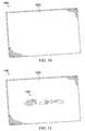
Figure 10 , an illustration of an embedded light source in a multilayer panel is depicted in accordance with an illustrative example.Multilayer panel 1000 may be a physical implementation ofmultilayer panel 202 shown in block form inFigure 2 .Multilayer panel 1000 may be one oflayup 800 orlayup 900 after processing. -
Multilayer panel 1000 hassurface 1002. In this illustrative example,surface 1002 is substantially uniform. As illustrated, the embedded light source (not depicted) is not visible when the embedded light source is not illuminated. As depicted, there is substantially no markoff onsurface 1002 from the embedded light source. - In some illustrative examples,
multilayer panel 1000 may be an example ofmultilayer panel 706 after adhering second layer ofmaterial 702. In these illustrative examples,surface 1002 may have some amount of markoff. In these illustrative examples, the embedded light source may be identified as a result of this markoff. - Turning now to
Figure 11 , an illustration of an illuminated embedded light source in a multilayer panel is depicted in accordance with an illustrative example.View 1100 may be a view ofmultilayer panel 1000 ofFigure 10 when the embedded light source is illuminated. As can be seen inview 1100, light from the embedded light source shines throughsurface 1102. In some illustrative examples, the embedded light source may be a dynamic display. In these illustrative examples,image 1104 may change as desired. In other illustrative examples, the embedded light source may be a static display. In these illustrative examples,image 1104 may be the same each time the embedded light source is illuminated. - Although
image 1104 is depicted as a fasten seat belt image,image 1104 may take any desirable form. Further,image 1104 as depicted does not limit the use ofmultilayer panel 1000 to implementations in an aircraft.Multilayer panel 1000 need not be present in an aircraft.Multilayer panel 1000 may be present in any desirable type of platform such as a mobile platform, a stationary platform, a land-based structure, an aquatic-based structure, and a space-based structure. More specifically, the platform may be a surface ship, a tank, a personnel carrier, a train, a spacecraft, a space station, a satellite, a submarine, an automobile, and other suitable platforms. - The
multilayer panel 1000 may be a standalone product.Multilayer panel 1000 may be a display panel which may be transported from location to location by an operator.Multilayer panel 1000 may be a component of any desirable mobile platform, stationary platform, or any desirable type of structure. For example,multilayer panel 1000 may be a component of a display board, an easel, or other type of display. In some illustrative examples,multilayer panel 1000 may be used to form furniture, free-standing lighting fixtures, wired lighting fixtures, or other desirable movable components. - The
multilayer panel 1000 may be a component of a school, a hospital, a museum, an exhibition hall, or any other desirable type of building. For example,multilayer panel 1000 may be used for a display or lighting. When not in use, the embedded light source may not be detectable. As a result,multilayer panel 1000 may be used to form walls, ceilings, partitions, or any desirable portion of a building. -
Multilayer panel 1000 may be manufactured as an original component of a platform. In some illustrative examples,multilayer panel 1000 may be a replacement or retrofitted component of a platform. For example, a composite panel inaircraft 100 without an embedded light source may be replaced withmultilayer panel 1000. In some illustrative examples, all or a portion of a wall of a building may be replaced withmultilayer panel 1000. - Yet further,
multilayer panel 1000 does not limit the size or shape of potential implementations ofmultilayer panel 1000.Multilayer panel 1000 may be created in any desirable size or shape. - Turning now to
Figure 12 , an illustration of a flowchart of a process for forming a multilayer panel with an embedded light source is depicted in accordance with an illustrative example.Process 1200 may be used inmanufacturing environment 200 ofFigure 2 to form a multilayer panel with an embedded light source such asmultilayer panel 202 with embeddedlight source 206 ofFigure 2 . - The process begins by associating a first electrode and a second electrode with a first layer of material (operation 1202). Associating the first electrode and the second electrode with the first layer of material includes affixing only one of the first electrode or the second electrode to the first layer of material. Affixing only one of the first electrode or the second electrode to the first layer of the material comprises at least one of adhering the only one of the first electrode or the second electrode to the first layer of material, printing the only one of the first electrode or the second electrode onto the first layer of material, or integrating conductive fibers into the first layer of material at selective locations to form the only one of the first electrode or the second electrode.
- By affixing only one of the first electrode or the second electrode, inconsistencies may be reduced in the resulting multilayer panel. For example, by having only one of the first electrode and the second electrode affixed to the first layer of material, delamination in the multilayer panel may be reduced or prevented. In some illustrative examples, associating also includes positioning the other of the first electrode or the second electrode such that the other of the first electrode or the second electrode is free to move relative to the first layer of material.
- The process then positions a light source in electrical communication with the first electrode and the second electrode (operation 1204). In some illustrative examples, positioning the light source in electrical communication with the first electrode and the second electrode includes bonding the light source to at least one of the first electrode or the second electrode. Bonding may include at least one of solder or conductive paste.
- The process may then process an assembly comprising the first layer of material, the first electrode, the second electrode, and the light source to form a multilayer panel with an embedded light source (operation 1206). Afterwards the process terminates.
- processing the assembly may include curing the first layer of material. In some illustrative examples, processing the assembly may include applying a laminate over the first layer of material and the light source. In some illustrative examples, the multilayer panel with embedded light source formed comprises at least one of cabin lighting, decor, advertising, emergency signage, emergency lighting, entertainment display, seat placards, or safety signage in an aircraft.
- The flowcharts and block diagrams in the different depicted examples illustrate the architecture, functionality, and operation of some possible implementations of apparatuses and methods in an illustrative example. In this regard, each block in the flowcharts or block diagrams may represent a module, a segment, a function, and/or a portion of an operation or step.
- The function or functions noted in the blocks may occur out of the order noted in the figures. For example, in some cases, two blocks shown in succession may be executed substantially concurrently, or the blocks may sometimes be performed in the reverse order, depending upon the functionality involved. Also, other blocks may be added in addition to the illustrated blocks in a flowchart or block diagram.
- For example, the process may further include applying a surface treatment to at least one of the light source or the first layer prior to processing the assembly panel. As another example, the process may further include placing a second layer of material over the light source and the first layer of material. In some illustrative examples, the first layer of material and the second layer of material are pre-impregnated composite materials, and processing the assembly comprises curing the assembly with at least one of applied heat or applied pressure to form a cured panel.
- In some illustrative examples, the second layer of material comprises a material that allows at least some light from the light source to travel through the second layer of material. In some illustrative examples, processing the assembly further comprises applying a laminate over the cured panel.
- The process may further include curing the first layer of material to form a cured panel after associating the first electrode and the second electrode with the first layer of material, wherein the light source is positioned in electrical communication with the first electrode and the second electrode on the cured panel, and wherein processing the multilayer panel comprises applying a laminate over the light source and the cured panel to form the multilayer panel with the embedded light source.
- In one example, the process further includes associating a shim having the approximate thickness of the light source with the first layer of material. The shim may be used to form a depression during processing of the multilayer panel.
- The illustrative examples of the disclosure may be described in the context of aircraft manufacturing and
service method 1300 as shown inFigure 13 andaircraft 1400 as shown inFigure 14 . Turning first toFigure 13 , a block diagram of an aircraft manufacturing and service method is depicted in accordance with an illustrative example. During pre-production, aircraft manufacturing andservice method 1300 may include specification anddesign 1302 ofaircraft 1400 ofFigure 14 andmaterial procurement 1304. - During production, component and
subassembly manufacturing 1306 andsystem integration 1308 ofaircraft 1400 ofFigure 14 takes place. Thereafter,aircraft 1400 ofFigure 14 may go through certification anddelivery 1310 in order to be placed inservice 1312. While inservice 1312 by a customer,aircraft 1400 ofFigure 14 is scheduled for routine maintenance andservice 1314, which may include modification, reconfiguration, refurbishment, and other maintenance or service. - Each of the processes of aircraft manufacturing and
service method 1300 may be performed or carried out by a system integrator, a third party, and/or an operator. In these examples, the operator may be a customer. For the purposes of this description, a system integrator may include, without limitation, any number of aircraft manufacturers and major-system subcontractors; a third party may include, without limitation, any number of vendors, subcontractors, and suppliers; and an operator may be an airline, a leasing company, a military entity, a service organization, and so on. - With reference now to
Figure 14 , a block diagram of an aircraft is depicted in which an illustrative example may be implemented. In this example,aircraft 1400 is produced by aircraft manufacturing andservice method 1300 ofFigure 13 and may includeairframe 1402 with plurality ofsystems 1404 and interior 1406. Examples ofsystems 1404 include one or more ofpropulsion system 1408,electrical system 1410,hydraulic system 1412, andenvironmental system 1414. Any number of other systems may be included. Although an aerospace example is shown, different illustrative examples may be applied to other industries, such as the automotive industry. Apparatuses and methods embodied herein may be employed during at least one of the stages of aircraft manufacturing andservice method 1300 ofFigure 13 . - The examples may be used during manufacturing and
service method 1300 ofFigure 13 . For example,multilayer panel 202 having embeddedlight source 206 ofFigure 2 may be formed during component andsubassembly manufacturing 1306. Further,multilayer panel 202 having embeddedlight source 206 ofFigure 2 may be inserted to replace a display in an aircraft during maintenance andservice 1314. - The illustrative examples present methods of forming embedded light sources in multilayer panels. By embedding a light source, such as an organic light emitting diode, in a composite panel, at least one of weight, bulk, or connection complexity may be decreased for pre-existing display locations. For example, brackets and mounting equipment may not be used with embedded light sources in multilayer panels. By eliminating brackets and mounting equipment in select locations, the weight of an aircraft may be reduced. Reduction in aircraft weight may contribute to a reduction in costs.
- Further, embedded light sources in multilayer panels may be used instead of conventionally unilluminated displays in some areas. Yet further, the number of displays in an aircraft may be reduced if embedded light sources are programmable displays. For example, the number of displays in an aircraft may be reduced if embedded light sources are capable of displaying multiple images in individual conventional displays.
- By embedding light sources into multilayer panels, the number of manufacturing steps in an aircraft may be reduced. For example, holes to install brackets and mounting equipment for displays may not be used. As a result, these manufacturing steps may be eliminated. By eliminating or reducing steps of manufacturing, at least one of manufacturing time or manufacturing cost may also be reduced.
- According to another aspect, there is provided a method comprising: associating a first electrode and a second electrode with a first layer of material; positioning a light source in electrical communication with the first electrode and the second electrode; and processing an assembly comprising the first layer of material, the first electrode, the second electrode, and the light source to form a multilayer panel with an embedded light source.
- Optionally, the method comprises: applying a surface treatment to at least one of the light source or the first layer of material prior to processing the assembly.
- Optionally, associating the first electrode and the second electrode with the first layer of material comprises affixing only one of the first electrode or the second electrode to the first layer of material.
- Optionally, associating the first electrode and the second electrode with the first layer of material further comprises: positioning an other of the first electrode or the second electrode such that the other of the first electrode or the second electrode is free to move relative to the first layer of material.
- Optionally, affixing only one of the first electrode or the second electrode to the first layer of material comprises at least one of adhering the only one of the first electrode or the second electrode to the first layer of material, printing the only one of the first electrode or the second electrode onto the first layer of material, or integrating conductive fibers into the first layer of material at selective locations to form the only one of the first electrode or the second electrode.
- Optionally, the method comprises: placing a second layer of material over the light source and the first layer of material.
- Optionally, the second layer of material comprises a material that allows at least some light from the light source to travel through the second layer of material.
- Optionally, the first layer of material and the second layer of material are pre-impregnated composite material, and wherein processing the assembly comprises: curing the assembly with at least one of applied heat or applied pressure to form a cured panel.
- Optionally, processing the assembly further comprises: applying a laminate over the cured panel.
- Optionally, the method comprises: curing the first layer of material to form a cured panel after associating the first electrode and the second electrode with the first layer of material, wherein the light source is positioned in electrical communication with the first electrode and the second electrode on the cured panel, and wherein processing the assembly comprises: applying a laminate over the light source and the cured panel to form the multilayer panel with the embedded light source.
- Optionally, the method comprises: associating a shim having an approximate thickness of the light source with the first layer of material.
- Optionally, the multilayer panel with the embedded light source comprises at least one of cabin lighting, decor, advertising, emergency signage, emergency lighting, entertainment display, seat placards, or safety signage.
- According to another aspect, there is provided a multilayer panel with an embedded light source comprising: a first electrode associated with a first layer of material; a second electrode associated with the first layer of material; a light source in electrical communication with the first electrode and the second electrode; and a second layer of material overlying the first layer of material and the light source.
- Optionally, the second layer of material is a laminate layer.
- Optionally, the light source rests substantially within a depression in the first layer of material.
- Optionally, the multilayer panel comprises: a conductive adhesive positioned between at least one of the first electrode or the second electrode and the light source.
- Optionally, the multilayer panel comprises: a layer of core material.
- Optionally, the second layer is a pre-impregnated composite material.
- Optionally, the multilayer panel has a non-planar curvature.
- Optionally, the light source is a static image flexible organic light emitting diode.
- Optionally, the light source is a programmable flexible organic light emitting diode.
- According to another aspect, there is provided an aircraft comprising: a multilayer panel with an embedded light source comprising a first electrode associated with a first layer of material, a second electrode associated with the first layer of material, a light source in electrical communication with the first electrode and the second electrode, and a second layer of material overlying the first layer of material and the light source; and a controller in communication with the light source.
- Optionally, the multilayer panel comprises at least one of cabin lighting, decor, advertising, emergency signage, emergency lighting, entertainment display, seat placards, or safety signage.
- According to another aspect, there is provided a multilayer panel with an embedded light source comprising: a first layer of composite material; a light source positioned relative to the first layer of composite material; and a second layer of composite material overlying the first layer of composite material and the light source.
- Optionally, the light source rests substantially within a depression in the first layer of composite material.
- The description of the different illustrative examples has been presented for purposes of illustration and description, and is not intended to be exhaustive or limited to the examples in the form disclosed. Many modifications and variations will be apparent to those of ordinary skill in the art. Further, different illustrative examples may provide different features as compared to other illustrative examples. The example or examples selected are chosen and described in order to best explain the principles of the examples, the practical application, and to enable others of ordinary skill in the art to understand the disclosure for various examples with various modifications as are suited to the particular use contemplated.
Claims (15)
- A method comprising:associating a first electrode (238) and a second electrode (240) with a first layer of material (223), preferably wherein associating the first electrode (238) and the second electrode (240) with the first layer of material (223) comprises affixing only one of the first electrode (238) or the second electrode (240) to the first layer of material (223);positioning a light source (208) in electrical communication with the first electrode (238) and the second electrode (240); andprocessing an assembly (207) comprising the first layer of material (223), the first electrode (238), the second electrode (240), and the light source (208) to form a multilayer panel (202) with an embedded light source (206).
- The method of claim 1 further comprising:applying a surface treatment (264) to at least one of the light source (208) or the first layer of material (223) prior to processing the assembly (207).
- The method of claim 1 or claim 2, wherein associating the first electrode (238) and the second electrode (240) with the first layer of material (223) further comprises:positioning another of the first electrode (238) or the second electrode (240) such that the other of the first electrode (238) or the second electrode (240) is free to move relative to the first layer of material (223).
- The method of any preceding claim, wherein affixing only one of the first electrode (238) or the second electrode (240) to the first layer of material (223) comprises at least one of adhering the only one of the first electrode (238) or the second electrode (240) to the first layer of material (223), printing the only one of the first electrode (238) or the second electrode (240) onto the first layer of material (223), or integrating conductive fibers into the first layer of material (223) at selective locations to form the only one of the first electrode (238) or the second electrode (240).
- The method of any preceding claim further comprising:placing a second layer of material (224) over the light source (208) and the first layer of material (223), preferably wherein the second layer of material (224) comprises a material that allows at least some light from the light source (208) to travel through the second layer of material (224).
- The method of claim 5, wherein the first layer of material (223) and the second layer of material (224) are pre-impregnated composite material, and wherein processing the assembly (207) comprises:curing the assembly (207) with at least one of applied heat or applied pressure to form a cured panel (279).
- The method of claim 6, wherein processing the assembly (207) further comprises:applying a laminate (226) over the cured panel (279).
- The method of any preceding claim further comprising:curing the first layer of material (223) to form a cured panel (279) after associating the first electrode (238) and the second electrode (240) with the first layer of material (223), wherein the light source (208) is positioned in electrical communication with the first electrode (238) and the second electrode (240) on the cured panel (279), and wherein processing the assembly (207) comprises:applying a laminate (226) over the light source (208) and the cured panel (279) to form the multilayer panel (202) with the embedded light source (206).
- The method of any preceding claim further comprising:associating a shim (272) having an approximate thickness of the light source (208) with the first layer of material (223).
- A multilayer panel (202) with an embedded light source (206) comprising:a first electrode (238) associated with a first layer of material (223);a second electrode (240) associated with the first layer of material (223);a light source (208) in electrical communication with the first electrode (238) and the second electrode (240); anda second layer of material (224) overlying the first layer of material (223) and the light source (208).
- The multilayer panel (202) of claim 10, wherein the second layer of material (224) is a laminate (226) layer.
- The multilayer panel (202) of claim 10 or claim 11, wherein the light source (208) rests substantially within a depression (225) in the first layer of material (223).
- The multilayer panel (202) of any of claims 10 to 12, further comprising:a conductive adhesive (252) positioned between at least one of the first electrode (238) or the second electrode (240) and the light source (208).
- The multilayer panel (202) of any of claims 10 to 13, wherein the second layer (224) is a pre-impregnated composite material (262).
- The multilayer panel (202) of any of claims 10 to 14, wherein the light source (208) is a static image (234) flexible (230) organic light emitting diode (228) or a programmable (232) flexible (230) organic light emitting diode (228).
Priority Applications (2)
| Application Number | Priority Date | Filing Date | Title |
|---|---|---|---|
| EP21163278.1A EP3854688A1 (en) | 2015-05-08 | 2016-04-21 | Structurally embedded lighting for display panels |
| EP17186698.1A EP3287369B1 (en) | 2015-05-08 | 2016-04-21 | Structurally embedded lighting for display panels |
Applications Claiming Priority (1)
| Application Number | Priority Date | Filing Date | Title |
|---|---|---|---|
| US14/707,652 US10099800B2 (en) | 2015-05-08 | 2015-05-08 | Structurally embedded lighting for display panels and method of making the same |
Related Child Applications (3)
| Application Number | Title | Priority Date | Filing Date |
|---|---|---|---|
| EP17186698.1A Division EP3287369B1 (en) | 2015-05-08 | 2016-04-21 | Structurally embedded lighting for display panels |
| EP17186698.1A Division-Into EP3287369B1 (en) | 2015-05-08 | 2016-04-21 | Structurally embedded lighting for display panels |
| EP21163278.1A Division EP3854688A1 (en) | 2015-05-08 | 2016-04-21 | Structurally embedded lighting for display panels |
Publications (2)
| Publication Number | Publication Date |
|---|---|
| EP3100951A1 true EP3100951A1 (en) | 2016-12-07 |
| EP3100951B1 EP3100951B1 (en) | 2019-10-23 |
Family
ID=55808426
Family Applications (3)
| Application Number | Title | Priority Date | Filing Date |
|---|---|---|---|
| EP16166352.1A Active EP3100951B1 (en) | 2015-05-08 | 2016-04-21 | Structurally embedded lighting for display panels |
| EP17186698.1A Active EP3287369B1 (en) | 2015-05-08 | 2016-04-21 | Structurally embedded lighting for display panels |
| EP21163278.1A Pending EP3854688A1 (en) | 2015-05-08 | 2016-04-21 | Structurally embedded lighting for display panels |
Family Applications After (2)
| Application Number | Title | Priority Date | Filing Date |
|---|---|---|---|
| EP17186698.1A Active EP3287369B1 (en) | 2015-05-08 | 2016-04-21 | Structurally embedded lighting for display panels |
| EP21163278.1A Pending EP3854688A1 (en) | 2015-05-08 | 2016-04-21 | Structurally embedded lighting for display panels |
Country Status (3)
| Country | Link |
|---|---|
| US (2) | US10099800B2 (en) |
| EP (3) | EP3100951B1 (en) |
| JP (1) | JP6892223B2 (en) |
Families Citing this family (3)
| Publication number | Priority date | Publication date | Assignee | Title |
|---|---|---|---|---|
| US10099800B2 (en) | 2015-05-08 | 2018-10-16 | The Boeing Company | Structurally embedded lighting for display panels and method of making the same |
| US10392129B1 (en) * | 2018-04-10 | 2019-08-27 | Rockwell Collins, Inc. | Integrated micro-LED luminous aircraft panel |
| US11800641B2 (en) * | 2019-06-14 | 2023-10-24 | Hutchinson Aeronautique & Industrie Ltée. | Composite panel comprising an integrated electrical circuit and manufacturing method thereof |
Citations (3)
| Publication number | Priority date | Publication date | Assignee | Title |
|---|---|---|---|---|
| US7391622B2 (en) * | 2004-05-19 | 2008-06-24 | The Boeing Company | Composite structural member having an integrated electrical circuit |
| WO2013148848A1 (en) * | 2012-03-28 | 2013-10-03 | Salvaggio David Jr | Carbon fiber shells for customizing the appearance of a vehicle |
| US8932905B1 (en) * | 2012-10-09 | 2015-01-13 | The Boeing Company | Semiconductor circuit system for a composite structure |
Family Cites Families (47)
| Publication number | Priority date | Publication date | Assignee | Title |
|---|---|---|---|---|
| US4788629A (en) * | 1986-10-29 | 1988-11-29 | Loctite Luminescent Systems, Inc. | Instrument panel members |
| US4819276A (en) | 1987-03-26 | 1989-04-11 | Stevens Robert B | Germicidal toilet seat |
| US6465951B1 (en) * | 1992-12-16 | 2002-10-15 | Durel Corporation | Electroluminescent lamp devices and their manufacture |
| US6054809A (en) * | 1996-08-14 | 2000-04-25 | Add-Vision, Inc. | Electroluminescent lamp designs |
| TW468283B (en) * | 1999-10-12 | 2001-12-11 | Semiconductor Energy Lab | EL display device and a method of manufacturing the same |
| JP2001351427A (en) * | 2000-06-08 | 2001-12-21 | Koito Mfg Co Ltd | Indicator lamp |
| US6672738B1 (en) * | 2000-11-22 | 2004-01-06 | James M. Lewis | Decorative ornament |
| TW546857B (en) * | 2001-07-03 | 2003-08-11 | Semiconductor Energy Lab | Light-emitting device, method of manufacturing a light-emitting device, and electronic equipment |
| US6583447B2 (en) * | 2001-08-27 | 2003-06-24 | Harvatek Corp. | Multiple LED chip package |
| DE10207641A1 (en) | 2002-02-22 | 2003-09-11 | Kid Systeme Gmbh | Information and display device for a supply unit of a passenger aircraft |
| US7169461B2 (en) * | 2002-10-17 | 2007-01-30 | Asahi Glass Company, Limited | Laminate, a substrate with wires, an organic EL display element, a connection terminal for the organic EL display element and a method for producing each |
| US7026660B2 (en) * | 2003-04-25 | 2006-04-11 | Osram Opto Semiconductors (Malaysia) Sdn. Bhd | Interconnection for organic devices |
| US7108392B2 (en) * | 2004-05-04 | 2006-09-19 | Eastman Kodak Company | Tiled flat panel lighting system |
| US20050248268A1 (en) * | 2004-05-05 | 2005-11-10 | World Properties, Inc. | Cloth textured EL lamp |
| JP4891554B2 (en) * | 2005-03-11 | 2012-03-07 | セイコーエプソン株式会社 | Display panel, mobile display module using the same, and electronic device |
| KR20070114810A (en) * | 2005-03-12 | 2007-12-04 | 쓰리엠 이노베이티브 프로퍼티즈 컴파니 | Illumination devices and methods for making the same |
| DE102006007285A1 (en) * | 2006-02-16 | 2007-08-30 | Airbus Deutschland Gmbh | Aircraft`s e.g. passenger aircraft, visualization system, has lining panel lining passenger cabin, where lining panel is coated with flexible display e.g. organic light emitting device display |
| US8779444B2 (en) * | 2006-11-03 | 2014-07-15 | Relume Technologies, Inc. | LED light engine with applied foil construction |
| US20080211652A1 (en) * | 2007-03-02 | 2008-09-04 | Nanolumens Acquisition, Inc. | Dynamic Vehicle Display System |
| DE102007011155A1 (en) | 2007-03-07 | 2008-09-18 | Airbus Deutschland Gmbh | Aircraft with a lighting device |
| US7857484B2 (en) | 2007-08-31 | 2010-12-28 | The Boeing Company | Lighting panels including embedded illumination devices and methods of making such panels |
| US8033684B2 (en) | 2007-08-31 | 2011-10-11 | The Boeing Company | Starry sky lighting panels |
| US7828456B2 (en) * | 2007-10-17 | 2010-11-09 | Lsi Industries, Inc. | Roadway luminaire and methods of use |
| KR100998233B1 (en) * | 2007-12-03 | 2010-12-07 | 서울반도체 주식회사 | Slim led package |
| DE102008016066A1 (en) * | 2008-03-28 | 2009-10-01 | Airbus Deutschland Gmbh | sandwich panel |
| JP5377985B2 (en) * | 2009-01-13 | 2013-12-25 | 株式会社東芝 | Semiconductor light emitting device |
| JP5533073B2 (en) * | 2010-03-16 | 2014-06-25 | セイコーエプソン株式会社 | Electro-optical device and illumination device |
| TW201110802A (en) | 2009-06-24 | 2011-03-16 | Seiko Epson Corp | Electro-optical device, electronic device, and illumination apparatus |
| JP5779182B2 (en) * | 2009-09-24 | 2015-09-16 | コーニンクレッカ フィリップス エヌ ヴェ | Wall or ceiling covering material |
| JP2011140264A (en) | 2010-01-07 | 2011-07-21 | Jamco Corp | Aircraft cabin lighting system |
| US20110279741A1 (en) | 2010-05-17 | 2011-11-17 | Inflight Investments Inc. | Flexible and contouring screen for aircraft passenger cabin |
| JP2011254285A (en) | 2010-06-02 | 2011-12-15 | Jamco Corp | Visible light radio communication apparatus for aircraft cabin amusement system |
| DE102010036795A1 (en) * | 2010-08-02 | 2012-02-02 | International Automotive Components Group Gmbh | Covering device for a motor vehicle with integrated lighting system |
| US20120043888A1 (en) * | 2010-08-18 | 2012-02-23 | Salter Stuart C | Vehicle Interior Light Configured to Color Correct and Method Thereof |
| US20120051067A1 (en) * | 2010-08-24 | 2012-03-01 | Key Plastics L.L.C. | Lighting display and method of manufacturing same |
| JP5932213B2 (en) * | 2010-11-12 | 2016-06-08 | 日本ガスケット株式会社 | Cylinder head gasket manufacturing method |
| US9023672B2 (en) * | 2012-01-18 | 2015-05-05 | Liteideas, Llc | Light emitting systems and methods |
| EP2620690A1 (en) * | 2012-01-26 | 2013-07-31 | Toshiba Lighting & Technology Corporation | Light-emitting circuit, luminaire, and manufacturing method for the light-emitting circuit |
| US9120517B2 (en) * | 2012-03-28 | 2015-09-01 | David Salvaggio, JR. | Carbon fiber shells for customizing the appearance of a vehicle |
| BE1020716A3 (en) * | 2012-06-19 | 2014-04-01 | Agc Glass Europe | GLASS ROOF COMPRISING MEANS FOR LIGHTING AND CONTROL OF THE LIGHT TRANSMISSION. |
| WO2014036217A2 (en) | 2012-08-29 | 2014-03-06 | Mag Aerospace Industries, Inc. | Aircraft galley and lavatory disinfection |
| US9324248B2 (en) * | 2012-09-04 | 2016-04-26 | The Boeing Company | Exterior aircraft display system |
| US20140115764A1 (en) | 2012-10-25 | 2014-05-01 | Ying Chang Cheng | The sanitization mechanism of the toilet seat |
| WO2014195801A2 (en) * | 2013-06-05 | 2014-12-11 | Brian Barrett | Modular light emitting diode lighting system |
| ES2781971T3 (en) * | 2013-06-28 | 2020-09-09 | Lumileds Holding Bv | Light emitting diode device |
| DE102014011170A1 (en) | 2014-07-29 | 2016-02-04 | Diehl Aircabin Gmbh | A light-emitting composite assembly and method of making the composite light-emitting assembly |
| US10099800B2 (en) | 2015-05-08 | 2018-10-16 | The Boeing Company | Structurally embedded lighting for display panels and method of making the same |
-
2015
- 2015-05-08 US US14/707,652 patent/US10099800B2/en active Active
-
2016
- 2016-04-21 EP EP16166352.1A patent/EP3100951B1/en active Active
- 2016-04-21 EP EP17186698.1A patent/EP3287369B1/en active Active
- 2016-04-21 EP EP21163278.1A patent/EP3854688A1/en active Pending
- 2016-04-22 JP JP2016085787A patent/JP6892223B2/en active Active
-
2018
- 2018-10-15 US US16/160,471 patent/US11511880B2/en active Active
Patent Citations (3)
| Publication number | Priority date | Publication date | Assignee | Title |
|---|---|---|---|---|
| US7391622B2 (en) * | 2004-05-19 | 2008-06-24 | The Boeing Company | Composite structural member having an integrated electrical circuit |
| WO2013148848A1 (en) * | 2012-03-28 | 2013-10-03 | Salvaggio David Jr | Carbon fiber shells for customizing the appearance of a vehicle |
| US8932905B1 (en) * | 2012-10-09 | 2015-01-13 | The Boeing Company | Semiconductor circuit system for a composite structure |
Also Published As
| Publication number | Publication date |
|---|---|
| JP6892223B2 (en) | 2021-06-23 |
| US10099800B2 (en) | 2018-10-16 |
| US20190084689A1 (en) | 2019-03-21 |
| US20160376024A1 (en) | 2016-12-29 |
| US11511880B2 (en) | 2022-11-29 |
| EP3854688A1 (en) | 2021-07-28 |
| EP3287369B1 (en) | 2021-08-11 |
| EP3287369A1 (en) | 2018-02-28 |
| EP3100951B1 (en) | 2019-10-23 |
| JP2017041433A (en) | 2017-02-23 |
Similar Documents
| Publication | Publication Date | Title |
|---|---|---|
| US11511880B2 (en) | Structurally embedded lighting for display panels | |
| US9718302B2 (en) | Decorative laminate with non-visible light activated material and system and method for using the same | |
| US10661710B2 (en) | Embedded lighting features for lighting panels | |
| US9855721B2 (en) | Nonwoven decorative laminates and methods of making the same | |
| EP3216690B1 (en) | Method for manufacturing a lining panel | |
| US20210138773A1 (en) | Fire-resistant, gas permeable decorative laminate | |
| US20200010035A1 (en) | Composite Panel Power System | |
| US10791386B2 (en) | Method of manufacturing a composite panel | |
| EP3235720B1 (en) | Active composite panel assemblies and methods | |
| US11074839B2 (en) | Method for conforming a display panel | |
| US11158219B2 (en) | Exterior lighting in aircraft livery | |
| US20200407038A1 (en) | Air grille panel assembly, system, and method of installing the same in a vehicle |
Legal Events
| Date | Code | Title | Description |
|---|---|---|---|
| PUAI | Public reference made under article 153(3) epc to a published international application that has entered the european phase |
Free format text: ORIGINAL CODE: 0009012 |
|
| STAA | Information on the status of an ep patent application or granted ep patent |
Free format text: STATUS: REQUEST FOR EXAMINATION WAS MADE |
|
| 17P | Request for examination filed |
Effective date: 20160421 |
|
| AK | Designated contracting states |
Kind code of ref document: A1 Designated state(s): AL AT BE BG CH CY CZ DE DK EE ES FI FR GB GR HR HU IE IS IT LI LT LU LV MC MK MT NL NO PL PT RO RS SE SI SK SM TR |
|
| AX | Request for extension of the european patent |
Extension state: BA ME |
|
| STAA | Information on the status of an ep patent application or granted ep patent |
Free format text: STATUS: EXAMINATION IS IN PROGRESS |
|
| 17Q | First examination report despatched |
Effective date: 20180926 |
|
| GRAP | Despatch of communication of intention to grant a patent |
Free format text: ORIGINAL CODE: EPIDOSNIGR1 |
|
| STAA | Information on the status of an ep patent application or granted ep patent |
Free format text: STATUS: GRANT OF PATENT IS INTENDED |
|
| INTG | Intention to grant announced |
Effective date: 20190523 |
|
| GRAS | Grant fee paid |
Free format text: ORIGINAL CODE: EPIDOSNIGR3 |
|
| GRAA | (expected) grant |
Free format text: ORIGINAL CODE: 0009210 |
|
| STAA | Information on the status of an ep patent application or granted ep patent |
Free format text: STATUS: THE PATENT HAS BEEN GRANTED |
|
| AK | Designated contracting states |
Kind code of ref document: B1 Designated state(s): AL AT BE BG CH CY CZ DE DK EE ES FI FR GB GR HR HU IE IS IT LI LT LU LV MC MK MT NL NO PL PT RO RS SE SI SK SM TR |
|
| REG | Reference to a national code |
Ref country code: GB Ref legal event code: FG4D |
|
| REG | Reference to a national code |
Ref country code: CH Ref legal event code: EP |
|
| REG | Reference to a national code |
Ref country code: IE Ref legal event code: FG4D |
|
| REG | Reference to a national code |
Ref country code: DE Ref legal event code: R096 Ref document number: 602016022774 Country of ref document: DE |
|
| REG | Reference to a national code |
Ref country code: AT Ref legal event code: REF Ref document number: 1193371 Country of ref document: AT Kind code of ref document: T Effective date: 20191115 |
|
| REG | Reference to a national code |
Ref country code: NL Ref legal event code: MP Effective date: 20191023 |
|
| REG | Reference to a national code |
Ref country code: LT Ref legal event code: MG4D |
|
| PG25 | Lapsed in a contracting state [announced via postgrant information from national office to epo] |
Ref country code: NL Free format text: LAPSE BECAUSE OF FAILURE TO SUBMIT A TRANSLATION OF THE DESCRIPTION OR TO PAY THE FEE WITHIN THE PRESCRIBED TIME-LIMIT Effective date: 20191023 Ref country code: BG Free format text: LAPSE BECAUSE OF FAILURE TO SUBMIT A TRANSLATION OF THE DESCRIPTION OR TO PAY THE FEE WITHIN THE PRESCRIBED TIME-LIMIT Effective date: 20200123 Ref country code: FI Free format text: LAPSE BECAUSE OF FAILURE TO SUBMIT A TRANSLATION OF THE DESCRIPTION OR TO PAY THE FEE WITHIN THE PRESCRIBED TIME-LIMIT Effective date: 20191023 Ref country code: PT Free format text: LAPSE BECAUSE OF FAILURE TO SUBMIT A TRANSLATION OF THE DESCRIPTION OR TO PAY THE FEE WITHIN THE PRESCRIBED TIME-LIMIT Effective date: 20200224 Ref country code: LT Free format text: LAPSE BECAUSE OF FAILURE TO SUBMIT A TRANSLATION OF THE DESCRIPTION OR TO PAY THE FEE WITHIN THE PRESCRIBED TIME-LIMIT Effective date: 20191023 Ref country code: SE Free format text: LAPSE BECAUSE OF FAILURE TO SUBMIT A TRANSLATION OF THE DESCRIPTION OR TO PAY THE FEE WITHIN THE PRESCRIBED TIME-LIMIT Effective date: 20191023 Ref country code: LV Free format text: LAPSE BECAUSE OF FAILURE TO SUBMIT A TRANSLATION OF THE DESCRIPTION OR TO PAY THE FEE WITHIN THE PRESCRIBED TIME-LIMIT Effective date: 20191023 Ref country code: NO Free format text: LAPSE BECAUSE OF FAILURE TO SUBMIT A TRANSLATION OF THE DESCRIPTION OR TO PAY THE FEE WITHIN THE PRESCRIBED TIME-LIMIT Effective date: 20200123 Ref country code: GR Free format text: LAPSE BECAUSE OF FAILURE TO SUBMIT A TRANSLATION OF THE DESCRIPTION OR TO PAY THE FEE WITHIN THE PRESCRIBED TIME-LIMIT Effective date: 20200124 Ref country code: PL Free format text: LAPSE BECAUSE OF FAILURE TO SUBMIT A TRANSLATION OF THE DESCRIPTION OR TO PAY THE FEE WITHIN THE PRESCRIBED TIME-LIMIT Effective date: 20191023 |
|
| PG25 | Lapsed in a contracting state [announced via postgrant information from national office to epo] |
Ref country code: IS Free format text: LAPSE BECAUSE OF FAILURE TO SUBMIT A TRANSLATION OF THE DESCRIPTION OR TO PAY THE FEE WITHIN THE PRESCRIBED TIME-LIMIT Effective date: 20200224 Ref country code: RS Free format text: LAPSE BECAUSE OF FAILURE TO SUBMIT A TRANSLATION OF THE DESCRIPTION OR TO PAY THE FEE WITHIN THE PRESCRIBED TIME-LIMIT Effective date: 20191023 Ref country code: HR Free format text: LAPSE BECAUSE OF FAILURE TO SUBMIT A TRANSLATION OF THE DESCRIPTION OR TO PAY THE FEE WITHIN THE PRESCRIBED TIME-LIMIT Effective date: 20191023 |
|
| PG25 | Lapsed in a contracting state [announced via postgrant information from national office to epo] |
Ref country code: AL Free format text: LAPSE BECAUSE OF FAILURE TO SUBMIT A TRANSLATION OF THE DESCRIPTION OR TO PAY THE FEE WITHIN THE PRESCRIBED TIME-LIMIT Effective date: 20191023 |
|
| REG | Reference to a national code |
Ref country code: DE Ref legal event code: R097 Ref document number: 602016022774 Country of ref document: DE |
|
| PG2D | Information on lapse in contracting state deleted |
Ref country code: IS |
|
| PG25 | Lapsed in a contracting state [announced via postgrant information from national office to epo] |
Ref country code: RO Free format text: LAPSE BECAUSE OF FAILURE TO SUBMIT A TRANSLATION OF THE DESCRIPTION OR TO PAY THE FEE WITHIN THE PRESCRIBED TIME-LIMIT Effective date: 20191023 Ref country code: CZ Free format text: LAPSE BECAUSE OF FAILURE TO SUBMIT A TRANSLATION OF THE DESCRIPTION OR TO PAY THE FEE WITHIN THE PRESCRIBED TIME-LIMIT Effective date: 20191023 Ref country code: ES Free format text: LAPSE BECAUSE OF FAILURE TO SUBMIT A TRANSLATION OF THE DESCRIPTION OR TO PAY THE FEE WITHIN THE PRESCRIBED TIME-LIMIT Effective date: 20191023 Ref country code: EE Free format text: LAPSE BECAUSE OF FAILURE TO SUBMIT A TRANSLATION OF THE DESCRIPTION OR TO PAY THE FEE WITHIN THE PRESCRIBED TIME-LIMIT Effective date: 20191023 Ref country code: DK Free format text: LAPSE BECAUSE OF FAILURE TO SUBMIT A TRANSLATION OF THE DESCRIPTION OR TO PAY THE FEE WITHIN THE PRESCRIBED TIME-LIMIT Effective date: 20191023 Ref country code: IS Free format text: LAPSE BECAUSE OF FAILURE TO SUBMIT A TRANSLATION OF THE DESCRIPTION OR TO PAY THE FEE WITHIN THE PRESCRIBED TIME-LIMIT Effective date: 20200223 |
|
| REG | Reference to a national code |
Ref country code: AT Ref legal event code: MK05 Ref document number: 1193371 Country of ref document: AT Kind code of ref document: T Effective date: 20191023 |
|
| PLBE | No opposition filed within time limit |
Free format text: ORIGINAL CODE: 0009261 |
|
| STAA | Information on the status of an ep patent application or granted ep patent |
Free format text: STATUS: NO OPPOSITION FILED WITHIN TIME LIMIT |
|
| PG25 | Lapsed in a contracting state [announced via postgrant information from national office to epo] |
Ref country code: SM Free format text: LAPSE BECAUSE OF FAILURE TO SUBMIT A TRANSLATION OF THE DESCRIPTION OR TO PAY THE FEE WITHIN THE PRESCRIBED TIME-LIMIT Effective date: 20191023 Ref country code: SK Free format text: LAPSE BECAUSE OF FAILURE TO SUBMIT A TRANSLATION OF THE DESCRIPTION OR TO PAY THE FEE WITHIN THE PRESCRIBED TIME-LIMIT Effective date: 20191023 Ref country code: IT Free format text: LAPSE BECAUSE OF FAILURE TO SUBMIT A TRANSLATION OF THE DESCRIPTION OR TO PAY THE FEE WITHIN THE PRESCRIBED TIME-LIMIT Effective date: 20191023 |
|
| 26N | No opposition filed |
Effective date: 20200724 |
|
| PG25 | Lapsed in a contracting state [announced via postgrant information from national office to epo] |
Ref country code: SI Free format text: LAPSE BECAUSE OF FAILURE TO SUBMIT A TRANSLATION OF THE DESCRIPTION OR TO PAY THE FEE WITHIN THE PRESCRIBED TIME-LIMIT Effective date: 20191023 Ref country code: AT Free format text: LAPSE BECAUSE OF FAILURE TO SUBMIT A TRANSLATION OF THE DESCRIPTION OR TO PAY THE FEE WITHIN THE PRESCRIBED TIME-LIMIT Effective date: 20191023 Ref country code: MC Free format text: LAPSE BECAUSE OF FAILURE TO SUBMIT A TRANSLATION OF THE DESCRIPTION OR TO PAY THE FEE WITHIN THE PRESCRIBED TIME-LIMIT Effective date: 20191023 |
|
| REG | Reference to a national code |
Ref country code: CH Ref legal event code: PL |
|
| PG25 | Lapsed in a contracting state [announced via postgrant information from national office to epo] |
Ref country code: LU Free format text: LAPSE BECAUSE OF NON-PAYMENT OF DUE FEES Effective date: 20200421 Ref country code: CH Free format text: LAPSE BECAUSE OF NON-PAYMENT OF DUE FEES Effective date: 20200430 Ref country code: LI Free format text: LAPSE BECAUSE OF NON-PAYMENT OF DUE FEES Effective date: 20200430 |
|
| REG | Reference to a national code |
Ref country code: BE Ref legal event code: MM Effective date: 20200430 |
|
| PG25 | Lapsed in a contracting state [announced via postgrant information from national office to epo] |
Ref country code: BE Free format text: LAPSE BECAUSE OF NON-PAYMENT OF DUE FEES Effective date: 20200430 |
|
| PG25 | Lapsed in a contracting state [announced via postgrant information from national office to epo] |
Ref country code: IE Free format text: LAPSE BECAUSE OF NON-PAYMENT OF DUE FEES Effective date: 20200421 |
|
| PG25 | Lapsed in a contracting state [announced via postgrant information from national office to epo] |
Ref country code: TR Free format text: LAPSE BECAUSE OF FAILURE TO SUBMIT A TRANSLATION OF THE DESCRIPTION OR TO PAY THE FEE WITHIN THE PRESCRIBED TIME-LIMIT Effective date: 20191023 Ref country code: MT Free format text: LAPSE BECAUSE OF FAILURE TO SUBMIT A TRANSLATION OF THE DESCRIPTION OR TO PAY THE FEE WITHIN THE PRESCRIBED TIME-LIMIT Effective date: 20191023 Ref country code: CY Free format text: LAPSE BECAUSE OF FAILURE TO SUBMIT A TRANSLATION OF THE DESCRIPTION OR TO PAY THE FEE WITHIN THE PRESCRIBED TIME-LIMIT Effective date: 20191023 |
|
| PG25 | Lapsed in a contracting state [announced via postgrant information from national office to epo] |
Ref country code: MK Free format text: LAPSE BECAUSE OF FAILURE TO SUBMIT A TRANSLATION OF THE DESCRIPTION OR TO PAY THE FEE WITHIN THE PRESCRIBED TIME-LIMIT Effective date: 20191023 |
|
| P01 | Opt-out of the competence of the unified patent court (upc) registered |
Effective date: 20230516 |
|
| PGFP | Annual fee paid to national office [announced via postgrant information from national office to epo] |
Ref country code: FR Payment date: 20230425 Year of fee payment: 8 Ref country code: DE Payment date: 20230427 Year of fee payment: 8 |
|
| PGFP | Annual fee paid to national office [announced via postgrant information from national office to epo] |
Ref country code: GB Payment date: 20230427 Year of fee payment: 8 |