EP3098872A1 - Organic light emitting display apparatus and method of manufacturing the same - Google Patents
Organic light emitting display apparatus and method of manufacturing the same Download PDFInfo
- Publication number
- EP3098872A1 EP3098872A1 EP15191845.5A EP15191845A EP3098872A1 EP 3098872 A1 EP3098872 A1 EP 3098872A1 EP 15191845 A EP15191845 A EP 15191845A EP 3098872 A1 EP3098872 A1 EP 3098872A1
- Authority
- EP
- European Patent Office
- Prior art keywords
- electrode
- pad
- auxiliary electrode
- auxiliary
- anode
- Prior art date
- Legal status (The legal status is an assumption and is not a legal conclusion. Google has not performed a legal analysis and makes no representation as to the accuracy of the status listed.)
- Granted
Links
Images



Classifications
-
- H—ELECTRICITY
- H10—SEMICONDUCTOR DEVICES; ELECTRIC SOLID-STATE DEVICES NOT OTHERWISE PROVIDED FOR
- H10D—INORGANIC ELECTRIC SEMICONDUCTOR DEVICES
- H10D86/00—Integrated devices formed in or on insulating or conducting substrates, e.g. formed in silicon-on-insulator [SOI] substrates or on stainless steel or glass substrates
- H10D86/40—Integrated devices formed in or on insulating or conducting substrates, e.g. formed in silicon-on-insulator [SOI] substrates or on stainless steel or glass substrates characterised by multiple TFTs
- H10D86/441—Interconnections, e.g. scanning lines
-
- H—ELECTRICITY
- H10—SEMICONDUCTOR DEVICES; ELECTRIC SOLID-STATE DEVICES NOT OTHERWISE PROVIDED FOR
- H10K—ORGANIC ELECTRIC SOLID-STATE DEVICES
- H10K59/00—Integrated devices, or assemblies of multiple devices, comprising at least one organic light-emitting element covered by group H10K50/00
- H10K59/10—OLED displays
- H10K59/12—Active-matrix OLED [AMOLED] displays
-
- H—ELECTRICITY
- H10—SEMICONDUCTOR DEVICES; ELECTRIC SOLID-STATE DEVICES NOT OTHERWISE PROVIDED FOR
- H10D—INORGANIC ELECTRIC SEMICONDUCTOR DEVICES
- H10D86/00—Integrated devices formed in or on insulating or conducting substrates, e.g. formed in silicon-on-insulator [SOI] substrates or on stainless steel or glass substrates
- H10D86/40—Integrated devices formed in or on insulating or conducting substrates, e.g. formed in silicon-on-insulator [SOI] substrates or on stainless steel or glass substrates characterised by multiple TFTs
- H10D86/451—Integrated devices formed in or on insulating or conducting substrates, e.g. formed in silicon-on-insulator [SOI] substrates or on stainless steel or glass substrates characterised by multiple TFTs characterised by the compositions or shapes of the interlayer dielectrics
-
- H—ELECTRICITY
- H10—SEMICONDUCTOR DEVICES; ELECTRIC SOLID-STATE DEVICES NOT OTHERWISE PROVIDED FOR
- H10D—INORGANIC ELECTRIC SEMICONDUCTOR DEVICES
- H10D86/00—Integrated devices formed in or on insulating or conducting substrates, e.g. formed in silicon-on-insulator [SOI] substrates or on stainless steel or glass substrates
- H10D86/40—Integrated devices formed in or on insulating or conducting substrates, e.g. formed in silicon-on-insulator [SOI] substrates or on stainless steel or glass substrates characterised by multiple TFTs
- H10D86/60—Integrated devices formed in or on insulating or conducting substrates, e.g. formed in silicon-on-insulator [SOI] substrates or on stainless steel or glass substrates characterised by multiple TFTs wherein the TFTs are in active matrices
-
- H—ELECTRICITY
- H10—SEMICONDUCTOR DEVICES; ELECTRIC SOLID-STATE DEVICES NOT OTHERWISE PROVIDED FOR
- H10K—ORGANIC ELECTRIC SOLID-STATE DEVICES
- H10K50/00—Organic light-emitting devices
- H10K50/80—Constructional details
- H10K50/805—Electrodes
-
- H—ELECTRICITY
- H10—SEMICONDUCTOR DEVICES; ELECTRIC SOLID-STATE DEVICES NOT OTHERWISE PROVIDED FOR
- H10K—ORGANIC ELECTRIC SOLID-STATE DEVICES
- H10K50/00—Organic light-emitting devices
- H10K50/80—Constructional details
- H10K50/805—Electrodes
- H10K50/81—Anodes
- H10K50/814—Anodes combined with auxiliary electrodes, e.g. ITO layer combined with metal lines
-
- H—ELECTRICITY
- H10—SEMICONDUCTOR DEVICES; ELECTRIC SOLID-STATE DEVICES NOT OTHERWISE PROVIDED FOR
- H10K—ORGANIC ELECTRIC SOLID-STATE DEVICES
- H10K50/00—Organic light-emitting devices
- H10K50/80—Constructional details
- H10K50/805—Electrodes
- H10K50/82—Cathodes
-
- H—ELECTRICITY
- H10—SEMICONDUCTOR DEVICES; ELECTRIC SOLID-STATE DEVICES NOT OTHERWISE PROVIDED FOR
- H10K—ORGANIC ELECTRIC SOLID-STATE DEVICES
- H10K50/00—Organic light-emitting devices
- H10K50/80—Constructional details
- H10K50/805—Electrodes
- H10K50/82—Cathodes
- H10K50/824—Cathodes combined with auxiliary electrodes
-
- H—ELECTRICITY
- H10—SEMICONDUCTOR DEVICES; ELECTRIC SOLID-STATE DEVICES NOT OTHERWISE PROVIDED FOR
- H10K—ORGANIC ELECTRIC SOLID-STATE DEVICES
- H10K50/00—Organic light-emitting devices
- H10K50/80—Constructional details
- H10K50/84—Passivation; Containers; Encapsulations
-
- H—ELECTRICITY
- H10—SEMICONDUCTOR DEVICES; ELECTRIC SOLID-STATE DEVICES NOT OTHERWISE PROVIDED FOR
- H10K—ORGANIC ELECTRIC SOLID-STATE DEVICES
- H10K59/00—Integrated devices, or assemblies of multiple devices, comprising at least one organic light-emitting element covered by group H10K50/00
- H10K59/10—OLED displays
- H10K59/12—Active-matrix OLED [AMOLED] displays
- H10K59/121—Active-matrix OLED [AMOLED] displays characterised by the geometry or disposition of pixel elements
-
- H—ELECTRICITY
- H10—SEMICONDUCTOR DEVICES; ELECTRIC SOLID-STATE DEVICES NOT OTHERWISE PROVIDED FOR
- H10K—ORGANIC ELECTRIC SOLID-STATE DEVICES
- H10K59/00—Integrated devices, or assemblies of multiple devices, comprising at least one organic light-emitting element covered by group H10K50/00
- H10K59/10—OLED displays
- H10K59/12—Active-matrix OLED [AMOLED] displays
- H10K59/121—Active-matrix OLED [AMOLED] displays characterised by the geometry or disposition of pixel elements
- H10K59/1213—Active-matrix OLED [AMOLED] displays characterised by the geometry or disposition of pixel elements the pixel elements being TFTs
-
- H—ELECTRICITY
- H10—SEMICONDUCTOR DEVICES; ELECTRIC SOLID-STATE DEVICES NOT OTHERWISE PROVIDED FOR
- H10K—ORGANIC ELECTRIC SOLID-STATE DEVICES
- H10K59/00—Integrated devices, or assemblies of multiple devices, comprising at least one organic light-emitting element covered by group H10K50/00
- H10K59/10—OLED displays
- H10K59/12—Active-matrix OLED [AMOLED] displays
- H10K59/122—Pixel-defining structures or layers, e.g. banks
-
- H—ELECTRICITY
- H10—SEMICONDUCTOR DEVICES; ELECTRIC SOLID-STATE DEVICES NOT OTHERWISE PROVIDED FOR
- H10K—ORGANIC ELECTRIC SOLID-STATE DEVICES
- H10K59/00—Integrated devices, or assemblies of multiple devices, comprising at least one organic light-emitting element covered by group H10K50/00
- H10K59/10—OLED displays
- H10K59/12—Active-matrix OLED [AMOLED] displays
- H10K59/123—Connection of the pixel electrodes to the thin film transistors [TFT]
-
- H—ELECTRICITY
- H10—SEMICONDUCTOR DEVICES; ELECTRIC SOLID-STATE DEVICES NOT OTHERWISE PROVIDED FOR
- H10K—ORGANIC ELECTRIC SOLID-STATE DEVICES
- H10K59/00—Integrated devices, or assemblies of multiple devices, comprising at least one organic light-emitting element covered by group H10K50/00
- H10K59/10—OLED displays
- H10K59/12—Active-matrix OLED [AMOLED] displays
- H10K59/124—Insulating layers formed between TFT elements and OLED elements
-
- H—ELECTRICITY
- H10—SEMICONDUCTOR DEVICES; ELECTRIC SOLID-STATE DEVICES NOT OTHERWISE PROVIDED FOR
- H10K—ORGANIC ELECTRIC SOLID-STATE DEVICES
- H10K59/00—Integrated devices, or assemblies of multiple devices, comprising at least one organic light-emitting element covered by group H10K50/00
- H10K59/10—OLED displays
- H10K59/12—Active-matrix OLED [AMOLED] displays
- H10K59/131—Interconnections, e.g. wiring lines or terminals
-
- H—ELECTRICITY
- H10—SEMICONDUCTOR DEVICES; ELECTRIC SOLID-STATE DEVICES NOT OTHERWISE PROVIDED FOR
- H10K—ORGANIC ELECTRIC SOLID-STATE DEVICES
- H10K59/00—Integrated devices, or assemblies of multiple devices, comprising at least one organic light-emitting element covered by group H10K50/00
- H10K59/80—Constructional details
- H10K59/805—Electrodes
-
- H—ELECTRICITY
- H10—SEMICONDUCTOR DEVICES; ELECTRIC SOLID-STATE DEVICES NOT OTHERWISE PROVIDED FOR
- H10K—ORGANIC ELECTRIC SOLID-STATE DEVICES
- H10K59/00—Integrated devices, or assemblies of multiple devices, comprising at least one organic light-emitting element covered by group H10K50/00
- H10K59/80—Constructional details
- H10K59/805—Electrodes
- H10K59/8051—Anodes
- H10K59/80516—Anodes combined with auxiliary electrodes, e.g. ITO layer combined with metal lines
-
- H—ELECTRICITY
- H10—SEMICONDUCTOR DEVICES; ELECTRIC SOLID-STATE DEVICES NOT OTHERWISE PROVIDED FOR
- H10K—ORGANIC ELECTRIC SOLID-STATE DEVICES
- H10K59/00—Integrated devices, or assemblies of multiple devices, comprising at least one organic light-emitting element covered by group H10K50/00
- H10K59/80—Constructional details
- H10K59/805—Electrodes
- H10K59/8052—Cathodes
- H10K59/80522—Cathodes combined with auxiliary electrodes
-
- H—ELECTRICITY
- H10—SEMICONDUCTOR DEVICES; ELECTRIC SOLID-STATE DEVICES NOT OTHERWISE PROVIDED FOR
- H10K—ORGANIC ELECTRIC SOLID-STATE DEVICES
- H10K59/00—Integrated devices, or assemblies of multiple devices, comprising at least one organic light-emitting element covered by group H10K50/00
- H10K59/80—Constructional details
- H10K59/805—Electrodes
- H10K59/8052—Cathodes
- H10K59/80524—Transparent cathodes, e.g. comprising thin metal layers
-
- H—ELECTRICITY
- H10—SEMICONDUCTOR DEVICES; ELECTRIC SOLID-STATE DEVICES NOT OTHERWISE PROVIDED FOR
- H10K—ORGANIC ELECTRIC SOLID-STATE DEVICES
- H10K71/00—Manufacture or treatment specially adapted for the organic devices covered by this subclass
-
- H—ELECTRICITY
- H10—SEMICONDUCTOR DEVICES; ELECTRIC SOLID-STATE DEVICES NOT OTHERWISE PROVIDED FOR
- H10K—ORGANIC ELECTRIC SOLID-STATE DEVICES
- H10K71/00—Manufacture or treatment specially adapted for the organic devices covered by this subclass
- H10K71/621—Providing a shape to conductive layers, e.g. patterning or selective deposition
-
- H—ELECTRICITY
- H10—SEMICONDUCTOR DEVICES; ELECTRIC SOLID-STATE DEVICES NOT OTHERWISE PROVIDED FOR
- H10K—ORGANIC ELECTRIC SOLID-STATE DEVICES
- H10K2102/00—Constructional details relating to the organic devices covered by this subclass
- H10K2102/301—Details of OLEDs
- H10K2102/302—Details of OLEDs of OLED structures
- H10K2102/3023—Direction of light emission
- H10K2102/3026—Top emission
-
- H—ELECTRICITY
- H10—SEMICONDUCTOR DEVICES; ELECTRIC SOLID-STATE DEVICES NOT OTHERWISE PROVIDED FOR
- H10K—ORGANIC ELECTRIC SOLID-STATE DEVICES
- H10K59/00—Integrated devices, or assemblies of multiple devices, comprising at least one organic light-emitting element covered by group H10K50/00
- H10K59/10—OLED displays
- H10K59/12—Active-matrix OLED [AMOLED] displays
- H10K59/1201—Manufacture or treatment
Definitions
- the present invention relates to an organic light emitting display apparatus, and more particularly, to a top emission type organic light emitting display apparatus and a method of manufacturing the same.
- Organic light emitting display apparatuses are self-emitting apparatuses and have low power consumption, a fast response time, high emission efficiency, high luminance, and a wide viewing angle.
- the organic light emitting display apparatuses are classified into a top emission type and a bottom emission type, based on a transmission direction of light emitted from an organic light emitting device.
- a circuit element is disposed between an emission layer and an image displaying surface, and for this reason, an aperture ratio is lowered.
- the circuit element is not disposed between the emission layer and the image displaying surface, and thus, an aperture ratio is enhanced.
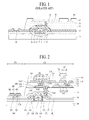
- FIG. 1 is a schematic cross-sectional view of a related art top emission type organic light emitting display apparatus.
- a thin film transistor (TFT) layer T which includes an active layer 11, a gate insulation layer 12, a gate electrode 13, an interlayer dielectric 14, a source electrode 15, and a drain electrode 16 is formed in an active area AA on a substrate 10, and a passivation layer 20 and a planarization layer 30 are sequentially formed on the TFT layer T.
- TFT thin film transistor
- An anode electrode 40 and an auxiliary electrode 50 are formed on the planarization layer 30.
- the auxiliary electrode 50 decreases a resistance of a cathode electrode 80 to be described below.
- a bank 60 is formed on the anode electrode 40 and the auxiliary electrode 50 and defines a pixel area.
- An organic emission layer 70 is formed in the pixel area defined by the bank 60, and the cathode electrode 80 is formed on the organic emission layer 70.
- the cathode electrode 80 is formed of a transparent conductive material, and a resistance of the cathode electrode 80 increases. In order to decrease the resistance of the cathode electrode 80, the cathode electrode 80 is connected to the auxiliary electrode 50.
- the gate insulation layer 12 and the interlayer dielectric 14 are formed in a pad area PA on the substrate 10, a signal pad 90 is formed on the interlayer dielectric 14, and the passivation layer 20 is formed on the signal pad 90.
- a hole is provided in the passivation layer 20, and the signal pad 90 is exposed to the outside through the hole. Since the signal pad 90 should be connected to an external driving circuit, the signal pad 90 is exposed to the outside by forming the hole in the passivation layer 20.
- the related art top emission type organic light emitting display apparatus has the following problems.
- the signal pad 90 Since the signal pad 90 should be connected to the external driving circuit, a top of the signal pad 90 is exposed to the outside. For this reason, the top of the signal pad 90 is corroded, and the corrosion is spread to another area.
- a metal layer which is excellent in corrosion resistance may be further formed on the top of the signal pad 90 so as to prevent the top of the signal pad 90 from being corroded, but in this case, the number of processes increases.
- an electrode layer which is the same as the anode electrode 40 may be formed on the signal pad 90 through the same process so as to prevent the top of the signal pad 90 from being corroded without an increase in number of processes. Even in this case, however, it is unable to prevent a material of the electrode material from being corroded, or it is unable to prevent corrosion from being spread through a side surface of the electrode layer.
- the top of the signal pad 90 is exposed by forming the hole in the passivation layer 20, but when the hole of the passivation layer 20 is previously formed, an etchant for pattern-forming the anode electrode 40 flows through the hole and damages the signal pad 90.
- a process of forming the hole of the passivation layer 20 for exposing the top of the signal pad 90 may be separately performed after a process of pattern-forming the anode electrode 40 is completed, but in this case, a separate mask process is added.
- the present invention is directed to provide a top emission type organic light emitting display apparatus and a method of manufacturing the same that substantially obviate one or more problems due to limitations and disadvantages of the related art.
- An aspect of the present invention is directed to provide a top emission type organic light emitting display apparatus and a method of manufacturing the same, in which the number of additional processes is minimized, and a signal pad is prevented from being corroded.
- an organic light emitting display apparatus in which an anode electrode, an organic emission layer, a cathode electrode, and an auxiliary electrode connected to the cathode electrode are disposed in an active area of a substrate, and a signal pad and a first pad electrode connected to the signal pad are disposed in a pad area of the substrate, wherein the auxiliary electrode includes a first auxiliary electrode and a second auxiliary electrode connected to the first auxiliary electrode through a contact hole, and the first pad electrode is formed of the same material as a material of the first auxiliary electrode.
- a method of manufacturing an organic light emitting display apparatus including: forming a source electrode and a signal pad on a substrate; forming a passivation layer on the source electrode and the signal pad; forming a first planarization layer on the passivation layer; forming a contact hole externally exposing the source electrode by removing a predetermined region of the passivation layer and a predetermined region of the first planarization layer and forming a contact hole externally exposing the signal pad by removing another partial region of the passivation layer; forming a first anode electrode connected to the source electrode, a first auxiliary electrode separated from the first anode electrode, and a first pad electrode connected to the signal pad; forming a second planarization layer on the first anode electrode and the first auxiliary electrode and forming a contact hole externally exposing each of the first anode electrode and the first auxiliary electrode by removing a partial region of the second planarization layer; and forming, on the second planarization
- FIG. 1 is a schematic cross-sectional view of a related art top emission type organic light emitting display apparatus
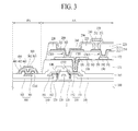
- FIG. 2 is a cross-sectional view of an organic light emitting display apparatus according to an embodiment of the present invention
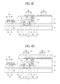
- FIG. 3 is a cross-sectional view of an organic light emitting display apparatus according to another embodiment of the present invention.
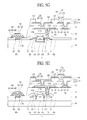
- FIGS. 4A to 4K are cross-sectional views illustrating a method of manufacturing an organic light emitting display apparatus according to an embodiment of the present invention.
- FIGS. 5A to 5H are cross-sectional views illustrating a method of manufacturing an organic light emitting display apparatus according to another embodiment of the present invention.
- first, second, etc. may be used herein to describe various elements, these elements should not be limited by these terms. These terms are only used to distinguish one element from another. For example, a first element could be termed a second element, and, similarly, a second element could be termed a first element, without departing from the scope of the present invention.
- FIG. 2 is a cross-sectional view of an organic light emitting display apparatus according to an embodiment of the present invention.
- the organic light emitting display apparatus may include an active area AA and a pad area PA which are included in a substrate 100.
- a thin film transistor (TFT) T may be formed in the active area AA of the substrate 100.
- TFT thin film transistor
- passivation layer 165 a passivation layer 165, a first planarization layer 171, a second planarization layer 172, a first anode electrode 180, a second anode electrode 200, a first auxiliary electrode 190, a second auxiliary electrode 210, a bank 220, a partition wall 230, an organic emission layer 240, and a cathode electrode 250 may be formed in the active area AA of the substrate 100.
- the TFT T may include an active layer 110, a gate insulation layer 120, a gate electrode 130, an interlayer dielectric 140, a source electrode 150, and a drain electrode 160.
- the active layer 110 may be formed on the substrate 100 to overlap the gate electrode 130.
- the active layer 110 may be formed of a silicon-based semiconductor material, or may be formed of an oxide-based semiconductor material.
- a light shielding layer may be further formed between the substrate 100 and the active layer 110, and in this case, external light incident through a bottom of the substrate 100 is blocked by the light shielding layer, thereby preventing the active layer 110 from being damaged by the external light.
- the gate insulation layer 120 may be formed on the active layer 110.
- the gate insulation layer 120 may insulate the active layer 110 from the gate electrode 130.
- the gate insulation layer 120 may be formed of an inorganic insulating material, for example, silicon oxide (SiOx), silicon nitride (SiNx), or a multilayer thereof, but is not limited thereto.
- the gate insulation layer 120 may extend to the pad area PA.
- the gate electrode 130 may be formed on the gate insulation layer 120.
- the gate electrode 130 may be formed to overlap the active layer 110 with the gate insulation layer 120 therebetween.
- the gate electrode 130 may be formed of a single layer or a multilayer formed of one of molybdenum (Mo), aluminum (Al), chromium (Cr), gold (Au), titanium (Ti), nickel (Ni), neodymium (Nd), and copper (Cu) or an alloy thereof, but is not limited thereto.
- the interlayer dielectric 140 may be formed on the gate electrode 130.
- the interlayer dielectric 140 may be formed of the same inorganic insulating material as that of the gate insulation layer 120, for example, silicon oxide (SiOx), silicon nitride (SiNx), or a multilayer thereof, but is not limited thereto.
- the interlayer dielectric 140 may extend to the pad area PA.
- the source electrode 150 and the drain electrode 160 may be formed to face each other on the interlayer dielectric 140.
- a first contact hole CH1 exposing one end region of the active layer 110 and a second contact hole CH2 exposing the other end region of the active layer 110 may be provided in the gate insulation layer 120 and the interlayer dielectric 140.
- the source electrode 150 may be connected to the other end region of the active layer 110 through the second contact hole CH2, and the drain electrode 160 may be connected to the one end region of the active layer 110 through the first contact hole CH1.
- the source electrode 150 may include a lower source electrode 151 and an upper source electrode 152.
- the lower source electrode 151 may be formed between the interlayer dielectric 140 and the upper source electrode 152 and may enhance an adhesive force between the interlayer dielectric 140 and the upper source electrode 152. Also, the lower source electrode 151 protects a bottom of the upper source electrode 152, thereby preventing the bottom of the upper source electrode 152 from being corroded. Therefore, an oxidation rate of the lower source electrode 151 may be lower than that of the upper source electrode 152. That is, the lower source electrode 151 may be formed of a material which is stronger in corrosion resistance than a material forming the upper source electrode 152. As described above, the lower source electrode 151 may act as an adhesion enhancement layer or an anti-corrosion layer and may be formed of an alloy (MoTi) of Mo and Ti, but is not limited thereto.
- MoTi alloy
- the upper source electrode 152 may be formed on a top of the lower source electrode 151.
- the upper source electrode 152 may be formed of Cu which is metal having a low resistance, but is not limited thereto.
- the upper source electrode 152 may be formed of metal which is relatively lower in resistance than the lower source electrode 151. In order to lower a total resistance of the source electrode 150, a thickness of the upper source electrode 152 may be formed thicker than that of the lower source electrode 151.
- the drain electrode 160 may include a lower drain electrode 161 and an upper drain electrode 162.
- the lower drain electrode 161 may be formed between the interlayer dielectric 140 and the upper drain electrode 162.
- the lower drain electrode 161 enhances an adhesive force between the interlayer dielectric 140 and the upper drain electrode 162 and moreover prevents a bottom of the upper drain electrode 162 from being corroded. Therefore, an oxidation rate of the lower drain electrode 161 may be lower than that of the upper drain electrode 162. That is, the lower drain electrode 161 may be formed of a material which is stronger in corrosion resistance than a material forming the upper drain electrode 162.
- the lower drain electrode 161 may be formed of an alloy (MoTi) of Mo and Ti which is the same as the above-described material of the lower source electrode 151, but is not limited thereto.
- the upper drain electrode 162 may be formed on a top of the lower drain electrode 161 and may be formed of Cu which is the same as the above-described material of the upper source electrode 152, but is not limited thereto. A thickness of the upper drain electrode 162 may be formed thicker than that of the lower drain electrode 161, thereby lowering a total resistance of the drain electrode 160.
- the upper drain electrode 162 may be formed of the same material as that of the upper source electrode 152 to have the same thickness as that of the upper source electrode 152, and the lower drain electrode 161 may be formed of the same material as that of the lower source electrode 151 to have the same thickness as that of the lower source electrode 151. In this case, the drain electrode 160 and the source electrode 150 may be simultaneously formed through the same process.
- a structure of the TFT T is not limited to the illustrated structure, and may be variously modified to structures known to those skilled in the art.
- a top gate structure where the gate electrode 130 is formed on the active layer 110 is illustrated in the drawing, but the TFT T may be formed in a bottom gate structure where the gate electrode 130 is formed under the active layer 110.
- the passivation layer 165 may be formed on the TFT T, and in more detail, may be formed on tops of the source electrode 150 and the drain electrode 160.
- the passivation layer 165 protects the TFT T.
- the passivation layer 165 may be formed of an inorganic insulating material (for example, SiOx and SiNx), but is not limited thereto.
- the passivation layer 165 may extend to the pad area PA.
- the first planarization layer 171 may be formed on the passivation layer 165.
- the first planarization layer 171 may planarize an upper surface of the substrate 100 including the TFT T.
- the first planarization layer 171 may be formed of an organic insulating material such as acryl resin, epoxy resin, phenolic resin, polyamide resin, polyimide resin, or the like, but is not limited thereto.
- the first planarization layer 171 may not extend to the pad area PA.
- the first anode electrode 180 and the first auxiliary electrode 190 may be formed on the first planarization layer 171. That is, the first anode electrode 180 and the first auxiliary electrode 190 may be formed on the same layer.
- a third contact hole CH3 exposing the source electrode 150 may be provided in the passivation layer 165 and the first planarization layer 171, and the source electrode 150 may be connected to the first anode electrode 180 through the third contact hole CH3.
- the first anode electrode 180 is connected with the source electrode 150.
- the source electrode 150 and the drain electrode 160 can be switched based on the mode of the transistor. Accordingly, in one or more embodiments, the first anode electrode 180 may be connected with the drain electrode 160 instead of the source electrode 150. As a result, the first anode electrode 180 may be connected with the source electrode 150 or the drain electrode 160.
- the first anode electrode 180 may include a first lower anode electrode 181, a first upper anode electrode 182, and a first cover anode electrode 183.
- the first lower anode electrode 181 may be formed between the first planarization layer 171 and the first upper anode electrode 182 and may enhance an adhesive force between the first planarization layer 171 and the first upper anode electrode 182. Also, the first lower anode electrode 181 protects a bottom of the first upper anode electrode 182, thereby preventing the bottom of the first upper anode electrode 182 from being corroded. Therefore, an oxidation rate of the first lower anode electrode 181 may be lower than that of the first upper anode electrode 182. That is, the first lower anode electrode 181 may be formed of a material which is stronger in corrosion resistance than a material forming the first upper anode electrode 182.
- the first upper anode electrode 181 protects a top of the upper source electrode 152, thereby preventing the top of the upper source electrode 152 from being corroded. Therefore, an oxidation rate of the first lower anode electrode 181 may be lower than that of the upper source electrode 152. That is, the first lower anode electrode 181 may be formed of a material which is stronger in corrosion resistance than a material forming the upper source electrode 152. As described above, the first lower anode electrode 181 prevents the top of the upper source electrode 152 from being corroded, and thus, the source electrode 150 may be formed in the above-described two-layer structure. The first lower anode electrode 181 may act as an adhesion enhancement layer or an anti-corrosion layer and may be formed of an alloy (MoTi) of Mo and Ti, but is not limited thereto.
- MoTi alloy
- the first upper anode electrode 182 may be formed between the first lower anode electrode 181 and the first cover anode electrode 183.
- the first upper anode electrode 182 may be formed of Cu which is metal having a low resistance, but is not limited thereto.
- the first upper anode electrode 182 may be formed of metal which is relatively lower in resistance than the first lower anode electrode 181.
- a thickness of the first upper anode electrode 182 may be formed thicker than that of each of the first lower anode electrode 181 and the first cover anode electrode 183.
- the first cover anode electrode 183 may be formed on the first upper anode electrode 182.
- the first cover anode electrode 183 may be formed to cover a top and a side surface of the first upper anode electrode 182, thereby preventing the first upper anode electrode 182 from being corroded.
- an oxidation rate of the first cover anode electrode 183 may be lower than that of the first upper anode electrode 182. That is, the first cover anode electrode 183 may be formed of a material which is stronger in corrosion resistance than a material forming the first upper anode electrode 182.
- the first cover anode electrode 183 may cover up to a side surface of the first lower anode electrode 181. In this case, an oxidation rate of the first cover anode electrode 183 may be lower than that of the first lower anode electrode 181. That is, the first cover anode electrode 183 may be formed of a material which is stronger in corrosion resistance than a material forming the first lower anode electrode 181. The first cover anode electrode 183 may be formed of a transparent conductive material such as indium tin oxide (ITO) or the like, but is not limited thereto.
- ITO indium tin oxide
- the first auxiliary electrode 190 may include a first lower auxiliary electrode 191, a first upper auxiliary electrode 192, and a first cover auxiliary electrode 183.
- the first lower auxiliary electrode 191 may be formed between the first planarization layer 171 and the first upper auxiliary electrode 192.
- the first lower auxiliary electrode 191 enhances an adhesive force between the first planarization layer 171 and the first upper auxiliary electrode 192 and moreover prevents a bottom of the first upper auxiliary electrode 192 from being corroded. Therefore, an oxidation rate of the first lower auxiliary electrode 191 may be lower than that of the first upper auxiliary electrode 192. That is, the first lower auxiliary electrode 191 may be formed of a material which is stronger in corrosion resistance than a material forming the first upper auxiliary electrode 192. As described above, the first lower auxiliary electrode 191 may be formed of an alloy (MoTi) of Mo and Ti which is the same as the above-described material of the first lower anode electrode 181, but is not limited thereto.
- the first upper auxiliary electrode 192 may be formed between the first lower auxiliary electrode 191 and the first cover auxiliary electrode 193 and may be formed of Cu which is the same as the above-described material of the first upper anode electrode 182, but is not limited thereto.
- a thickness of the first upper auxiliary electrode 192 which is relatively low in resistance may be formed thicker than that of each of the first lower auxiliary electrode 191 and the first cover auxiliary electrode 193 which are relatively high in resistance, thereby lowering a total resistance of the first auxiliary electrode 190.
- the first cover auxiliary electrode 193 may be formed on the first upper auxiliary electrode 192.
- the first cover auxiliary electrode 193 may be formed to cover a top and a side surface of the first upper auxiliary electrode 192, thereby preventing the first upper auxiliary electrode 192 from being corroded.
- an oxidation rate of the first cover auxiliary electrode 193 may be lower than that of the first upper auxiliary electrode 192. That is, the first cover auxiliary electrode 193 may be formed of a material which is stronger in corrosion resistance than a material forming the first upper auxiliary electrode 192.
- the first cover auxiliary electrode 193 may cover up to a side surface of the first lower auxiliary electrode 191. In this case, an oxidation rate of the first cover auxiliary electrode 193 may be lower than that of the first lower auxiliary electrode 191. That is, the first cover auxiliary electrode 193 may be formed of a material which is stronger in corrosion resistance than a material forming the first lower auxiliary electrode 191.
- the first cover auxiliary electrode 193 may be formed of a transparent conductive material such as ITO or the like, but is not limited thereto.
- the first cover auxiliary electrode 193 may be formed of the same material as that of the first cover anode electrode 183 to have the same thickness as that of the first cover anode electrode 183
- the first upper auxiliary electrode 192 may be formed of the same material as that of the first upper anode electrode 182 to have the same thickness as that of the first upper anode electrode 182
- the first lower auxiliary electrode 191 may be formed of the same material as that of the first lower anode electrode 181 to have the same thickness as that of the first lower anode electrode 181.
- the first auxiliary electrode 190 and the first anode electrode 180 may be simultaneously formed through the same process.
- the second planarization layer 172 may be formed on the first auxiliary electrode 190 and the first anode electrode 180.
- the second planarization layer 172 may planarize an upper surface of the substrate 100 along with the above-described first planarization layer 171.
- the second planarization layer 172 may be formed of an organic insulating material such as acryl resin, epoxy resin, phenolic resin, polyamide resin, polyimide resin, or the like, but is not limited thereto.
- the second planarization layer 172 may not extend to the pad area PA.
- a fourth contact hole CH4 and a fifth contact hole CH5 may be included in the second planarization layer 172.
- the first anode electrode 180 may be exposed by the fourth contact hole CH4, and the first auxiliary electrode 190 may be exposed by the fifth contact hole CH5.
- the second anode electrode 200 may be formed on the second planarization layer 172.
- the second anode electrode 200 may be connected to the first anode electrode 180 through the fourth contact hole CH4.
- the second anode electrode 200 may reflect light, emitted from the organic emission layer 240, in an upward direction, and to this end, the second anode electrode 200 may be formed of a material having good reflectivity.
- the second anode electrode 200 may include a second lower anode electrode 201, a second center anode electrode 202, and a second upper anode electrode 203.
- the second lower anode electrode 201 may be formed between the first anode electrode 180 and the second center anode electrode 202.
- the second lower anode electrode 201 protects a bottom of the second center anode electrode 202, thereby preventing the bottom of the second center anode electrode 202 from being corroded.
- an oxidation rate of the second lower anode electrode 201 may be lower than that of the second center anode electrode 202. That is, the second lower anode electrode 201 may be formed of a material which is stronger in corrosion resistance than a material forming the second center anode electrode 202.
- the second lower anode electrode 201 may be formed of a transparent conductive material such as ITO or the like, but is not limited thereto.
- the second center anode electrode 202 may be formed between the second lower anode electrode 201 and the second upper anode electrode 203.
- the second center anode electrode 202 may be formed of a material which is lower in resistance than and better in reflectivity than the second lower anode electrode 201 and the second upper anode electrode 203, and for example, may be formed of silver (Ag).
- a thickness of the second center anode electrode 202 which is relatively low in resistance may be formed thicker than that of each of the second lower anode electrode 201 and the second upper anode electrode 203 which are relatively high in resistance, thereby lowering a total resistance of the second anode electrode 200.
- the second upper anode electrode 203 may be formed on a top of the second center anode electrode 202, thereby preventing the top of the second center anode electrode 202 from being corroded. To this end, an oxidation rate of the second upper anode electrode 203 may be lower than that of the second center anode electrode 202. That is, the second upper anode electrode 203 may be formed of a material which is stronger in corrosion resistance than a material forming the second center anode electrode 202.
- the second upper anode electrode 203 may be formed of a transparent conductive material such as ITO or the like, but is not limited thereto.
- the second auxiliary electrode 210 may be formed on the second planarization layer 172 identically to the second anode electrode 200.
- the second auxiliary electrode 210 may be connected to the first auxiliary electrode 190 through the fifth contact hole CH5.
- the second auxiliary electrode 210 may lower a resistance of the cathode electrode 250 along with the first auxiliary electrode 190.
- the second auxiliary electrode 210 may include a second lower auxiliary electrode 211, a second center auxiliary electrode 212, and a second upper auxiliary electrode 213.
- the second lower auxiliary electrode 211 may be formed between the first auxiliary electrode 190 and the second center auxiliary electrode 212.
- the second lower auxiliary electrode 211 protects a bottom of the second center auxiliary electrode 212, thereby preventing the bottom of the second center auxiliary electrode 212 from being corroded.
- an oxidation rate of the second lower auxiliary electrode 211 may be lower than that of the second center auxiliary electrode 212. That is, the second lower auxiliary electrode 211 may be formed of a material which is stronger in corrosion resistance than a material forming the second center auxiliary electrode 212.
- the second lower auxiliary electrode 211 may be formed of a transparent conductive material such as ITO or the like, but is not limited thereto.
- the second center auxiliary electrode 212 may be formed between the second lower auxiliary electrode 211 and the second upper auxiliary electrode 213.
- the second center auxiliary electrode 212 may be formed of a material which is lower in resistance than and better in reflectivity than the second lower auxiliary electrode 211 and the second upper auxiliary electrode 213, and for example, may be formed of silver (Ag).
- a thickness of the second center auxiliary electrode 212 which is relatively low in resistance may be formed thicker than that of each of the second lower auxiliary electrode 211 and the second upper auxiliary electrode 213 which are relatively high in resistance, thereby lowering a total resistance of the second auxiliary electrode 210.
- the second upper auxiliary electrode 213 may be formed on a top of the second center auxiliary electrode 212, thereby preventing the top of the second center auxiliary electrode 212 from being corroded. To this end, an oxidation rate of the second upper auxiliary electrode 213 may be lower than that of the second center auxiliary electrode 212. That is, the second upper auxiliary electrode 213 may be formed of a material which is stronger in corrosion resistance than a material forming the second center auxiliary electrode 212.
- the second upper auxiliary electrode 213 may be formed of a transparent conductive material such as ITO or the like, but is not limited thereto.
- the second upper auxiliary electrode 213 may be formed of the same material as that of the second upper anode electrode 203 to have the same thickness as that of the second upper anode electrode 203
- the second center auxiliary electrode 212 may be formed of the same material as that of the second center anode electrode 202 to have the same thickness as that of the second center anode electrode 202
- the second lower auxiliary electrode 211 may be formed of the same material as that of the second lower anode electrode 201 to have the same thickness as that of the second lower anode electrode 201.
- the second auxiliary electrode 210 and the second anode electrode 200 may be simultaneously formed through the same process.
- two auxiliary electrodes (for example, the first and second auxiliary electrodes 190 and 210) connected to each other may be formed for lowering the resistance of the cathode electrode 250, and thus, the desired resistance characteristic of an auxiliary electrode is more easily adjusted.
- the second auxiliary electrode 210 is formed on the same layer as a layer on which the second anode electrode 200 is disposed, a width of the second anode electrode 200 should be reduced when a width of the second auxiliary electrode 210 increases, and in this case, a pixel area of a display apparatus is reduced. For this reason, there is a limitation in increasing the width of the second auxiliary electrode 210. Therefore, according to an embodiment of the present invention, the first auxiliary electrode 190 connected to the second auxiliary electrode 210 may be further formed under the second auxiliary electrode 210, and thus, the resistance of the cathode electrode 150 is effectively lowered even without any reduction in a pixel area.
- the first auxiliary electrode 190 may be formed on the same layer as a layer on which the first anode electrode 180 is disposed, and since the first anode electrode 180 connects the source electrode 150 to the second anode electrode 200, a width of the first anode electrode 180 is reduced, thereby increasing a width of the first auxiliary electrode 190. That is, the width of the first auxiliary electrode 190 may be formed greater than that of the first anode electrode 180, and moreover, the width of first auxiliary electrode 190 may increase in order for the first auxiliary electrode 190 to overlap the second anode electrode 200, whereby the resistance of the cathode electrode 150 is more effectively lowered.
- the bank 220 may be formed on the second anode electrode 200 and the second auxiliary electrode 210.
- the bank 220 may be formed on one side and the other side of the second anode electrode 200 to expose a top of the second anode electrode 200. Since the bank 220 is formed to expose the top of the second anode electrode 200, an area where an image is displayed is secured. Also, since the bank 220 is formed on the one side and the other side of the second anode electrode 200, a side surface of the second center anode electrode 202 vulnerable to corrosion is prevented from being exposed to the outside, thereby preventing the side surface of the second center anode electrode 202 from being corroded.
- the bank 220 may be formed on one side and the other side of the second auxiliary electrode 210 to expose a top of the second auxiliary electrode 210. Since the bank 220 is formed to expose the top of the second auxiliary electrode 210, an electrical connection space between the second auxiliary electrode 210 and the cathode electrode 250 is secured. Also, since the bank 220 is formed on the one side and the other side of the second auxiliary electrode 210, a side surface of the second center auxiliary electrode 212 vulnerable to corrosion is prevented from being exposed to the outside, thereby preventing the side surface of the second center auxiliary electrode 212 from being corroded.
- the bank 220 may be formed between the second anode electrode 200 and the second auxiliary electrode 210 and may insulate the second anode electrode 200 from the second auxiliary electrode 210.
- the bank 220 may be formed of an organic insulating material such as polyimide resin, acryl resin, benzocyclobutene (BCB), or the like, but is not limited thereto.
- the partition wall 230 may be formed on the second auxiliary electrode 210.
- the partition wall 230 may be separated from the bank 220 by a certain distance, and the second auxiliary electrode 210 may be electrically connected to the cathode electrode 250 through a separation space between the partition wall 230 and the bank 220.
- the second auxiliary electrode 210 may be electrically connected to the cathode electrode 250 without forming the partition wall 230.
- the organic emission layer 240 is more easily deposition-formed. This will be described below in more detail.
- a mask pattern which covers a top of the second auxiliary electrode 210 is needed in depositing the organic emission layer 240, in order for the top of the second auxiliary electrode 210 not to be covered by the organic emission layer 240.
- a top of the partition wall 230 may act as eaves in depositing the organic emission layer 240, and thus, since the organic emission layer 240 is not deposited under the eaves, the mask pattern which covers the top of the second auxiliary electrode 210 is not needed.
- the organic emission layer 240 cannot penetrate into the separation space between the partition wall 230 and the bank 220, and thus, the second auxiliary electrode 210 may be exposed in the separation space between the partition wall 230 and the bank 220.
- the organic emission layer 240 may be formed by a deposition process such as an evaporation process which is excellent in straightness of a deposited material, and thus, the organic emission layer 240 is not deposited in the separation space between the partition wall 230 and the bank 220.
- a width of the top of the partition wall 230 may be formed greater than that of a bottom of the partition wall 230, in order for the top of the partition wall 230 to act as the eaves.
- the partition wall 230 may include a lower first partition wall 231 and an upper second partition wall 232.
- the first partition wall 231 may be formed on a top of the second auxiliary electrode 210 and may be formed of the same material as that of the bank 220 through the same process as that of the bank 220.
- the second partition wall 232 may be formed on a top of the first partition wall 231.
- a width of a top of the second partition wall 232 may be formed greater than that of a bottom of the second partition wall 232, and particularly, the top of the second partition wall 232 may be formed to cover the separation space between the partition wall 230 and the bank 220 and may act as eaves.
- the organic emission layer 240 may be formed on the second anode electrode 200.
- the organic emission layer 240 may include a hole injection layer, a hole transport layer, an emission layer, an electron transport layer, and an electron injection layer.
- the organic emission layer 240 may be modified to have various structures known to those skilled in the art.
- the organic emission layer 240 may extend to the top of the bank 220. However, the organic emission layer 240 may not extend to the top of the second auxiliary electrode 210 in a state of covering the top of the second auxiliary electrode 210. This is because when the organic emission layer 240 covers the top of the second auxiliary electrode 210, it is difficult to electrically connect the second auxiliary electrode 210 to the cathode electrode 250. As described above, the organic emission layer240 may be formed by a deposition process without a mask that covers the top of the second auxiliary electrode 210, and in this case, the organic emission layer 240 may be formed on the top of the partition wall 230.
- the cathode electrode 250 may be formed on the organic emission layer 240.
- the cathode electrode 250 may be formed on a surface from which light is emitted, and thus may be formed of a transparent conductive material. Since the cathode electrode 250 is formed of a transparent conductive material, a resistance of the cathode electrode 250 is high, and for this reason, in order to lower the resistance of the cathode electrode 250, the cathode electrode 250 may be connected to the second auxiliary electrode 210. That is, the cathode electrode 250 may be connected to the second auxiliary electrode 210 through the separation space between the partition wall 230 and the bank 220.
- the cathode electrode 250 may be formed by a deposition process such as a sputtering process which is not good in straightness of a deposited material, and thus, the cathode electrode 250 may be deposited in the separation space between the partition wall 230 and the bank 220 in a process of depositing the cathode electrode 250.
- an encapsulation layer may be further formed on the cathode electrode 250 and prevents penetration of water.
- the encapsulation layer may use various materials known to those skilled in the art.
- a color filter may be further formed for each pixel and on the cathode electrode 250, and in this case, white light may be emitted from the organic emission layer 240.
- the gate insulation layer 120, the interlayer dielectric 140, the signal pad 300, the passivation layer 165, and a first pad electrode 400 may be formed in the pad area PA of the substrate 100.
- the gate insulation layer 120 may be formed on the substrate 100, and the interlayer dielectric 140 may be formed on the gate insulation layer 120.
- the gate insulation layer 120 and the interlayer dielectric 140 may extend from the active area AA and may be formed all over the pad area PA.
- the signal pad 300 may be formed on the interlayer dielectric 140.
- the signal pad 300 may be formed on the same layer as a layer where the source electrode 150 and the drain electrode 160 in the active area AA are disposed.
- the signal pad 300 may include a lower signal pad 301 and an upper signal pad 302.
- the lower signal pad 301 may be formed between the interlayer dielectric 140 and the upper signal pad 302 and may enhance an adhesive force between the interlayer dielectric 140 and the upper signal pad 302. Also, the lower signal pad 301 prevents a bottom of the upper signal pad 302 from being corroded. Therefore, an oxidation rate of the lower signal pad 301 may be lower than that of the upper signal pad 302. That is, the lower signal pad 301 may be formed of a material which is stronger in corrosion resistance than a material forming the upper signal pad 302. As described above, the lower signal pad 301 may be formed of an alloy (MoTi) of Mo and Ti which is the same as the above-described material of the lower source electrode 151 or the lower drain electrode 161, but is not limited thereto.
- MoTi alloy of Mo and Ti which is the same as the above-described material of the lower source electrode 151 or the lower drain electrode 161, but is not limited thereto.
- the upper signal pad 302 may be formed on a top of the lower signal pad 301.
- the upper signal pad 302 may be formed of Cu which is metal having a low resistance, but is not limited thereto.
- the upper signal pad 302 may be formed of metal which is relatively lower in resistance than the lower signal pad 301.
- a thickness of the upper signal pad 302 may be formed thicker than that of the lower signal pad 301.
- the upper signal pad 302 may be formed of the same material as that of the upper source electrode 152 and/or the upper drain electrode 162 to have the same thickness as that of the upper source electrode 152 and/or the upper drain electrode 162, and the lower signal pad 301 may be formed of the same material as that of the lower source electrode 151 and/or the lower drain electrode 161 to have the same thickness as that of the lower source electrode 151 and/or the lower drain electrode 161.
- the signal pad 300 and the source electrode 150, the signal pad 300 and the drain electrode 160, or the signal pad 300, the source electrode 150, and the drain electrode 160 may be simultaneously formed through the same process.
- the passivation layer 165 may be formed on the signal pad 300.
- the passivation layer 165 may extend from the active area AA.
- a sixth contact hole CH6 exposing a portion of the signal pad 300 may be included in the passivation layer 165.
- the first pad electrode 400 may be formed on the passivation layer 165.
- the first pad electrode 400 may be connected to the signal pad 300 through the sixth contact hole CH6.
- the first pad electrode 400 may be exposed to the outside and connected to an external driver.
- the first pad electrode 400 protects a top of the signal pad 300.
- the top of the signal pad 300 may be configured by the upper signal pad 302 which is relatively vulnerable to corrosion, and thus, the first pad electrode 400 may be formed to cover the top of the upper signal pad 302 exposed through the sixth contact hole CH6, thereby preventing the upper signal pad 302 from being corroded.
- the signal pad 300 may be formed in the above-described two-layer structure.
- An oxidation rate of the first pad electrode 400, particularly, an oxidation rate of the first cover pad electrode 403, may be lower than that of the upper signal pad 302.
- the first pad electrode 400 particularly, the first cover pad electrode 403, may be formed of a material which is stronger in corrosion resistance than a material forming the upper signal pad 302. Also, since the first pad electrode 400 is exposed to the outside, the first cover pad electrode 403 corresponding to an uppermost surface of the first pad electrode 400 may be formed of a material which is strong in corrosion resistance.
- the first pad electrode 400 may be formed of the same material as that of the first anode electrode 180 and/or the first auxiliary electrode 190 to have the same thickness as that of the first anode electrode 180 and/or the first auxiliary electrode 190. In this case, the first pad electrode 400 and the first anode electrode 180 and/or the first auxiliary electrode 190 may be pattern-formed through the same mask process.
- the first pad electrode 400 may include a first lower pad electrode 401, a first upper pad electrode 402, and a first cover pad electrode 403.
- the first lower pad electrode 401 may be formed to cover a top of the upper signal pad 302 through the sixth contact hole CH6, thereby preventing the upper signal pad 302 from being corroded. To this end, an oxidation rate of the first lower pad electrode 401 may be lower than that of the upper signal pad 302. That is, the first lower pad electrode 401 may be formed of a material which is stronger in corrosion resistance than a material forming the upper signal pad 302. As described above, the first lower pad electrode 401 prevents the top of the upper signal pad 302 from being corroded, and thus, the signal pad 300 may be formed in the above-described two-layer structure.
- the first lower pad electrode 401 may be formed of an alloy (MoTi) of Mo and Ti which is the same as the above-described material of the first lower anode electrode 181 and/or the first lower auxiliary electrode 191, but is not limited thereto.
- the first lower pad electrode 401 may be formed of the same material as that of the first lower anode electrode 181 and/or the first lower auxiliary electrode 191 to have the same thickness as that of the first lower anode electrode 181 and/or the first lower auxiliary electrode 191, and in this case, the first lower pad electrode 401 and the first lower anode electrode 181, the first lower pad electrode 401 and the first lower auxiliary electrode 191, or the first lower pad electrode 401, the first lower anode electrode 181, and the first lower auxiliary electrode 191 may be pattern-formed through the same mask process.
- the first upper pad electrode 402 may be formed between the first lower pad electrode 401 and the first cover pad electrode 403.
- the first upper pad electrode 402 may be formed of Cu which is metal having a low resistance, but is not limited thereto.
- the first upper pad electrode 402 may be formed of metal which is relatively lower in resistance than the first lower pad electrode 401 and the first cover pad electrode 403. In order to lower a total resistance of the first pad electrode 400, a thickness of the first upper pad electrode 402 may be formed thicker than that of each of the first lower pad electrode 401 and the first cover pad electrode 403.
- the first upper pad electrode 402 may be formed of the same material as that of the first upper anode electrode 182 and/or the first upper auxiliary electrode 192 to have the same thickness as that of the first upper anode electrode 182 and/or the first upper auxiliary electrode 192, and in this case, the first upper pad electrode 402 and the first upper anode electrode 182, the first upper pad electrode 402 and the first upper auxiliary electrode 192, or the first upper pad electrode 402, the first upper anode electrode 182, and the first upper auxiliary electrode 192 may be pattern-formed through the same mask process.
- the first cover pad electrode 403 may be formed on the first upper pad electrode 402.
- the first cover pad electrode 403 may be formed to cover a top and a side surface of the first upper pad electrode 402, thereby preventing the first upper pad electrode 402 from being corroded. That is, the first cover pad electrode 403 prevents the first upper pad electrode 402 from being exposed to the outside.
- an oxidation rate of the first cover pad electrode 403 may be lower than that of the first upper pad electrode 402. That is, the first cover pad electrode 403 may be formed of a material which is stronger in corrosion resistance than a material forming the first upper pad electrode 402.
- the first cover pad electrode 403 may cover up to a side surface of the first lower pad electrode 401. In this case, an oxidation rate of the first cover pad electrode 403 may be lower than that of the first lower pad electrode 401. That is, the first cover pad electrode 403 may be formed of a material which is stronger in corrosion resistance than a material forming the first lower pad electrode 401. The first cover pad electrode 403 may be formed of a transparent conductive material such as ITO or the like, but is not limited thereto.
- the first cover pad electrode 403 may be formed of the same material as that of the first cover anode electrode 183 and/or the first cover auxiliary electrode 193 to have the same thickness as that of the first cover anode electrode 183 and/or the first cover auxiliary electrode 193, and in this case, the first cover pad electrode 403 and the first cover anode electrode 183, the first cover pad electrode 403 and the first cover auxiliary electrode 193, or the first cover pad electrode 403, the first cover anode electrode 183, and the first cover auxiliary electrode 193 may be pattern-formed through the same mask process.
- FIG. 3 is a cross-sectional view of an organic light emitting display apparatus according to another embodiment of the present invention. Except that structures of a second anode electrode 200 and a second auxiliary electrode 210 are changed and a second pad electrode 500 is further provided, the organic light emitting display apparatus of FIG. 3 is the same as the above-described organic light emitting display apparatus of FIG. 2 . Thus, like reference numerals refer to like elements. Hereinafter, only elements different from the above-described elements of FIG. 2 will be described in detail.
- the second anode electrode 200 may include a second center anode electrode 202 and a second upper anode electrode 203, and the second lower anode electrode 201 is omitted.
- the second auxiliary electrode 210 may include a second center auxiliary electrode 212 and a second upper auxiliary electrode 213, and the second lower auxiliary electrode 211 is omitted.
- the second center anode electrode 202 and the second center auxiliary electrode 212 may be formed of a material such as an alloy (MoTi) of Mo and Ti which are good in reflectivity and is good in corrosion resistance, but is not limited thereto.
- MoTi an alloy of Mo and Ti which are good in reflectivity and is good in corrosion resistance, but is not limited thereto.
- the second pad electrode 500 may be further formed on the first pad electrode 400. Since the second pad electrode 500 is further provided, a height of a pad part increases, and a contact area increases, whereby the second pad electrode 500 is more easily connected to an external driver.
- the second pad electrode 500 may be formed of the same material as that of the second anode electrode 200 and/or the second auxiliary electrode 210 having a two-layer structure to have the same thickness as that of the second anode electrode 200 and/or the second auxiliary electrode 210, and in this case, the second pad electrode 500 and the second anode electrode 200, the second pad electrode 500 and the second auxiliary electrode 210, or the second pad electrode 500, the second anode electrode 200, and the second auxiliary electrode 210 may be pattern-formed through the same mask process.
- the second pad electrode 500 may include a second center pad electrode 502 and a second upper pad electrode 503.
- the second center pad electrode 502 may be formed of the same material as that of the second center anode electrode 202 and/or the second center auxiliary electrode 212
- the second upper pad electrode 503 may be formed of the same material as that of the second upper anode electrode 203 and/or the second upper auxiliary electrode 213.
- a side surface of the second center pad electrode 502 is exposed to the outside, but since the second center pad electrode 502 is formed of a material which is good in corrosion resistance, the second center pad electrode 502 is prevented from being corroded. Also, the second upper pad electrode 503 is exposed to the outside, but since the second upper pad electrode 503 is formed of a material which is good in corrosion resistance, the second upper pad electrode 503 is prevented from being corroded.
- FIGS. 4A to 4K are cross-sectional views illustrating a method of manufacturing an organic light emitting display apparatus according to an embodiment of the present invention and relate to a method of manufacturing the above-described organic light emitting display apparatus of FIG. 2 .
- like reference numerals refer to like elements, and in a material and a structure of each element, the same or similar descriptions are not repeated.
- an active layer 110, a gate insulation layer 120, a gate electrode 130, an interlayer dielectric 140, a source electrode 150, a drain electrode 160, and a signal pad 300 may be sequentially formed on a substrate 100.
- the active layer 110 may be formed on the substrate 100, the gate insulation layer 120 may be formed on the active layer 110, the gate electrode 130 may be formed on the gate insulation layer 120, the interlayer dielectric 140 may be formed on the gate electrode 130, and a first contact hole CH1 and a second contact hole CH2 may be formed in the gate insulation layer 120 and the interlayer dielectric 140.
- the drain electrode 160 which is connected to one end region of the active layer 110 through the first contact hole CH1, the source electrode 150 which is connected to the other end region of the active layer 110 through the second contact hole CH2, and the signal pad 300 may be formed.
- the active layer 110, the gate electrode 130, the source electrode 150, and the drain electrode 160 may be formed in an active area AA
- the gate insulation layer 120 and the interlayer dielectric 140 may be formed to extend from the active area AA to a pad area PA
- the signal pad 300 may be formed in the pad area AA.
- a TFT T may be formed in the active area AA
- the signal pad 300 may be formed in the pad area PA.
- the source electrode 150 may be configured with a lower source electrode 151 and an upper source electrode 152
- the drain electrode 160 may be configured with a lower drain electrode 161 and an upper drain electrode 162
- the signal pad 300 may be configured with a lower signal pad 301 and an upper signal pad 302.
- the source electrode 150, the drain electrode 160, and the signal pad 300 may be simultaneously formed of the same material by the same patterning process.
- a passivation layer 165 may be formed on the source electrode 150, the drain electrode 160, and the signal pad 300, and a first planarization layer 171 may be formed on the passivation layer 165.
- the passivation layer 165 may be formed to extend from the active area AA to the pad area PA, and the first planarization layer 171 may be formed in the active area AA.
- the passivation layer165 and the first planarization layer 171 may be formed to include a third contact hole CH3 in the active area AA, and the source electrode 150 may be exposed to the outside through the third contact hole CH3. Also, the passivation layer 165 may be formed to include a sixth contact hole CH6 in the pad area PA, and the signal pad 300 may be exposed to the outside through the sixth contact hole CH6.
- the third contact hole CH3 for externally exposing the source electrode 150 and the sixth contact hole CH6 for externally exposing the signal pad 300 may be simultaneously formed, and thus, the third contact hole CH3 and the sixth contact hole CH6 may be formed through one mask process, thereby preventing the number of mask processes from increasing.
- the exposed upper signal pad 302 may be covered by a lower pad electrode 401 in a process of FIG. 4C to be described below, and thus, the etchant cannot be brought in contact with the upper signal pad 302.
- the sixth contact CH6 and the third contact hole CH3 may be simultaneously formed.
- a first anode electrode 180 and a first auxiliary electrode 190 may be formed to be separated from each other on the first planarization layer 171 in the active area AA, and a first pad electrode 400 may be formed on the passivation layer 165 in the pad area PA.
- the first anode electrode 180 may be formed to be connected to the source electrode 150 through the third contact hole CH3, and the first pad electrode 400 may be formed to be connected to the signal pad 300 through the sixth contact hole CH6. In other embodiment, the first anode electrode 180 may be formed to be connected to the drain electrode 160 through the third contact hole CH3 formed to expose the drain electrode 160.
- the first anode electrode 180 may be configured with a first lower anode electrode 181, a first upper anode electrode 182, and a first cover anode electrode 183.
- the first auxiliary electrode 190 may be configured with a first lower auxiliary electrode 191, a first upper auxiliary electrode 192, and a first cover auxiliary electrode 193.
- the first pad electrode 400 may be configured with a first lower pad electrode 401, a first upper pad electrode 402, and a first cover pad electrode 403.
- the first anode electrode 180, the first auxiliary electrode 190, and the first pad electrode 400 may be simultaneously formed of the same material through the same patterning process.
- a second planarization layer 172 may be formed on a first anode electrode 180 and a first auxiliary electrode 190 in the active area AA.
- the second planarization layer 173 may be formed to include a fourth contact hole CH4 and a fifth contact hole CH5.
- the first anode electrode 180 may be exposed to the outside through the fourth contact hole CH4, and the first auxiliary electrode 190 may be exposed to the outside through the fifth contact hole CH5.
- the first photoresist pattern 610 may be formed on the first pad electrode 400 in the pad area PA.
- the first pad electrode 400 may be covered by the first photoresist pattern 610 and thus may not be exposed to the outside.
- the first photoresist pattern 610 may not be formed (e.g. may be omitted) in the active area AA.
- an electrode layer for a second anode electrode (see 200 of FIG. 4G ) and a second auxiliary electrode (see 210 of FIG. 4G ) may be formed in the pad area PA and the active area AA.
- a lower electrode layer 1, an intermediate electrode layer 2, and an upper electrode layer 3 may be sequentially formed on the first photoresist pattern 610 in the pad area PA and the second planarization layer 172 in the active area AA.
- a second photoresist pattern 620 may be formed on the electrode layer, in more detail, the upper electrode layer 3 in the active area AA.
- a second anode electrode 200 and a second auxiliary electrode 210 may be formed by etching the lower electrode layer 1, the intermediate electrode layer 2, and the upper electrode layer 3 with the second photoresist pattern 620 as a mask.
- the second photoresist pattern 620 may be formed as a pattern corresponding to a pattern of each of the second anode electrode 200 and the second auxiliary electrode 210. Therefore, a portion of the lower electrode layer 1, a portion of the intermediate electrode layer 2, and a portion of the upper electrode layer 3 which are not covered by the second photoresist pattern 620 may be removed by the etching process, and portions covered by the second photoresist pattern 620 may be left, thereby forming the pattern of each of the second anode electrode 200 and the second auxiliary electrode 210. As a result, the second anode electrode 200 and the second auxiliary electrode 210 may be simultaneously formed of the same material through the same patterning process.
- the second anode electrode 200 may include a second lower anode electrode 201, a second center anode electrode 202, and a second upper anode electrode 203.
- the second auxiliary electrode 210 may include a second lower auxiliary electrode 211, a second center auxiliary electrode 212, and a second upper auxiliary electrode 213.
- the first pad electrode 400 is not damaged by an etchant because the first photoresist pattern 610 covers the first pad electrode 400.
- the first photoresist pattern 610 and the second photoresist pattern 620 may be removed by a strip process. Therefore, the pad electrode 400, the second anode electrode 200, and the second auxiliary electrode 210 may be exposed to the outside.
- FIGS. 4E to 4H relate to a method of forming the second anode electrode 200 and the second auxiliary electrode 210 without the first pad electrode 400 being damaged.
- the first photoresist pattern 610 may be formed on the first pad electrode 400 to cover the first pad electrode 400, and thus, the first pad electrode 400 is not damaged by an etchant in forming the pattern of each of the second anode electrode 200 and the second auxiliary electrode 210. Also, since the first photoresist pattern 610 is removed simultaneously with the second photoresist pattern 620, a manufacturing process is simplified.
- the second planarization layer 172 may be formed to cover the first pad electrode 400 by extending the second planarization layer 172 to the pad area PA, and then, the second anode electrode 200 and the second auxiliary electrode 210 may be formed, in the above-described process of FIG. 4D .
- a process of removing a region of the second planarization layer 172 extending to the pad area PA through an oxygen (O 2 ) ashing process should be further performed after the second anode electrode 200 and the second auxiliary electrode 210 are formed, for externally exposing the first pad electrode 400.
- a photoresist pattern should be further formed as a mask for the process of removing the region of the second planarization layer 172 extending to the pad area PA, and moreover, due to the oxygen (O 2 ) ashing process, the inside of a chamber is contaminated, and a process time increases. Therefore, as described above with reference to FIGS. 4E to 4H , the first photoresist pattern 610 may be preferably used.
- a bank 220 may be formed on one side and the other side of the second anode electrode 200 to expose a top of the second anode electrode 200. Also, the bank 220 may be formed on one side and the other side of the second auxiliary electrode 210 to expose a top of the second auxiliary electrode 210.
- first partition wall 231 and a second partition wall 232 may be sequentially formed on the exposed top of the second auxiliary electrode 210.
- the first partition wall 231 may be formed of the same material as that of the bank 220 through the same pattern forming process as that of the bank 220 simultaneously with the bank 220.
- the partition wall 230 may be formed to be separated from the bank 220 by a certain distance, and thus, a separation space may be provided between the partition wall 230 and the bank 220.
- a width of a top of the second partition wall 232 may be formed greater than that of a bottom of the second partition wall 232.
- the top of the second partition wall 232 may cover the separation space between the partition wall 230 and the bank 220, and thus, in a below-described process of depositing an organic emission layer 240, the organic emission layer 240 is not deposited in the separation space between the partition wall 230 and the bank 220.
- the organic emission layer 240 may be formed on the second anode electrode 200.
- the organic emission layer 240 may be formed by a deposition process such as an evaporation process which is excellent in straightness of a deposited material, and thus, the organic emission layer 240 may be deposited on tops of the bank 220 and the partition wall 230, but the organic emission layer 240 is not deposited in the separation space between the partition wall 230 and the bank 220.
- the top of the partition wall 230 may act as the eaves in depositing the organic emission layer 240, and thus, even when the organic emission layer 240 is deposited without a mask pattern which covers the top of the second auxiliary electrode 210, the organic emission layer 240 is not deposited in the separation space between the partition wall 230 and the bank 220.
- a cathode electrode 250 may be formed on the organic emission layer 240.
- the cathode electrode 250 may be formed to be connected to the second auxiliary electrode 210 through the separation space between the partition wall 230 and the bank 220.
- the cathode electrode 250 may be formed by a deposition process such as a sputtering process which is not good in straightness of a deposited material, and thus, the cathode electrode 250 may be deposited in the separation space between the partition wall 230 and the bank 220 in a process of depositing the cathode electrode 250.
- FIGS. 5A to 5H are cross-sectional views illustrating a method of manufacturing an organic light emitting display apparatus according to another embodiment of the present invention and relate to a method of manufacturing the above-described organic light emitting display apparatus of FIG. 3 .
- FIGS. 5A to 5H are cross-sectional views illustrating a method of manufacturing an organic light emitting display apparatus according to another embodiment of the present invention and relate to a method of manufacturing the above-described organic light emitting display apparatus of FIG. 3 .
- descriptions repetitive of the above-described embodiment are omitted.
- an active layer 110, a gate insulation layer 120, a gate electrode 130, an interlayer dielectric 140, a source electrode 150, a drain electrode 160, and a signal pad 300 may be sequentially formed on a substrate 100. Therefore, a TFT T may be formed in the active area AA, and the signal pad 300 may be formed in the pad area PA.
- a process is the same as the above-described process of FIG. 4A .
- a passivation layer 165 may be formed on the source electrode 150, the drain electrode 160, and the signal pad 300, and a first planarization layer 171 may be formed on the passivation layer 165.
- the passivation layer 165 and the first planarization layer 171 may be formed to include a third contact hole CH3 in the active area AA, and the source electrode 150 may be exposed to the outside through the third contact hole CH3. Also, the passivation layer 165 may be formed to include a sixth contact hole CH6 in the pad area PA, and the signal pad 300 may be exposed to the outside through the sixth contact hole CH6. Such a process is the same as the above-described process of FIG. 4B .
- a first anode electrode 180 and a first auxiliary electrode 190 may be formed on the first planarization layer 171 in the active area AA, and a first pad electrode 400 may be formed on the passivation layer 165 in the pad area PA.
- the first anode electrode 180 may be formed to be connected to the source electrode 150 through the third contact hole CH3, and the first pad electrode 400 may be formed to be connected to the signal pad 300 through the sixth contact hole CH6.
- Such a process is the same as the above-described process of FIG. 4C .
- a second planarization layer 172 may be formed on the first anode electrode 180 and the first auxiliary electrode 190 in the active area AA.
- the second planarization layer 173 may be formed to include a fourth contact hole CH4 and a fifth contact hole CH5, the fist anode electrode 180 may be exposed to the outside through the fourth contact hole CH4, and the first auxiliary electrode 190 may be exposed to the outside through the fifth contact hole CH5.
- a process is the same as the above-described process of FIG. 4D .
- a second anode electrode 200 and a second auxiliary electrode 210 may be formed on the second planarization layer 172 in the active area AA, and a second pad electrode 500 may be formed on the first pad electrode 400 in the pad area PA.
- the second anode electrode 200 may be connected to the first anode electrode 180 through the fourth contact hole CH4, the second auxiliary electrode 210 may be connected to the second anode electrode 190 through the fifth contact hole CH5, and the second pad electrode 500 may be directly formed on a top of the first pad electrode 400.
- the second anode electrode 200 may include a second center anode electrode 202 and a second upper anode electrode 203
- the second auxiliary electrode 210 may include a second center auxiliary electrode 212 and a second upper auxiliary electrode 213
- the second pad electrode 500 may include a second center pad electrode 502 and a second upper pad electrode 503.
- the second anode electrode 200, the second auxiliary electrode 210, and the second pad electrode 500 may be simultaneously formed of the same material through the same patterning process, and thus, a mask process is not added.
- a first cover pad electrode 403 formed on an uppermost surface of the first pad electrode 400 may be formed of the same material (for example, ITO which is good in corrosion resistance) as that of the second upper pad electrode 503 formed on an uppermost surface of the second pad electrode 500, and in this case, when the second pad electrode 500 is pattern-formed, it is required to prevent a pattern of the first cover pad electrode 403 from being damaged.
- ITO which is good in corrosion resistance
- the second pad electrode 500 may be formed through a process where an electrode material for the second center pad electrode 502 and an electrode material for the second upper pad electrode 503 are sequentially deposited, the second upper pad electrode 503 is pattern-formed by etching the electrode material for the second center pad electrode 502, and the second center pad electrode 502 is subsequently pattern-formed by etching the electrode material for the second upper pad electrode 503.
- the first cover pad electrode 403 is covered by the electrode material for the second center pad electrode 502 when etching the electrode material for the second upper pad electrode 503, and thus, an etchant for etching the electrode material for the second upper pad electrode 503 is not brought in contact with the first cover pad electrode 403, thereby preventing a pattern of the first upper pad electrode 403 from being damaged.
- a bank 220 may be formed on one side and the other side of the second anode electrode 200 to expose a top of the second anode electrode 200.
- the bank 220 may be formed on one side and the other side of the second auxiliary electrode 210 to expose a top of the second auxiliary electrode 210.
- a first partition wall 231 and a second partition wall 232 may be sequentially formed on the exposed top of the second auxiliary electrode 210.
- the partition wall 230 may be formed to be separated from the bank 220 by a certain distance, and thus, a separation space may be provided between the partition wall 230 and the bank 220. Such a process is the same as the above-described process of FIG. 4I .
- an organic emission layer 240 may be formed on the second anode electrode 200.
- the organic emission layer 240 may be deposited on tops of the bank 220 and the partition wall 230, but is not deposited in the separation space between the partition wall 230 and the bank 220. Such a process is the same as the above-described process of FIG. 4J .
- a cathode electrode 250 may be formed on the organic emission layer 240.
- the cathode electrode 250 may be formed to be connected to the second auxiliary electrode 210 through the separation space between the partition wall 230 and the bank 220.
- Such a process is the same as the above-described process of FIG. 4K .
- the first pad electrode may be formed to cover the top of the signal pad, thereby preventing the signal pad from being corroded.
- the signal pad may be formed in a two-layer structure which includes the lower signal pad and the upper signal pad vulnerable to corrosion.
- the first pad electrode and the first auxiliary electrode are simultaneously formed of the same material, the number of mask processes does not increase.
- the contact hole for externally exposing the source electrode and the contact hole for externally exposing the signal pad may be simultaneously formed, and thus, the number of mask processes does not increase.
- the two auxiliary electrodes may be formed for lowering the resistance of the cathode electrode, and thus, the desired resistance characteristic of the auxiliary electrode is more easily adjusted.
- the first auxiliary electrode connected to the second auxiliary electrode through the contact hole may be further formed under the second auxiliary electrode, the resistance of the cathode electrode is effectively lowered even without any reduction in a pixel area.
Landscapes
- Engineering & Computer Science (AREA)
- Microelectronics & Electronic Packaging (AREA)
- Physics & Mathematics (AREA)
- Optics & Photonics (AREA)
- Manufacturing & Machinery (AREA)
- Geometry (AREA)
- Electroluminescent Light Sources (AREA)
Abstract
Description
- This application claims the benefit of the Korean Patent Application No.
10-2015-0075397 filed on May 28, 2015 - The present invention relates to an organic light emitting display apparatus, and more particularly, to a top emission type organic light emitting display apparatus and a method of manufacturing the same.
- Organic light emitting display apparatuses are self-emitting apparatuses and have low power consumption, a fast response time, high emission efficiency, high luminance, and a wide viewing angle.
- The organic light emitting display apparatuses are classified into a top emission type and a bottom emission type, based on a transmission direction of light emitted from an organic light emitting device. In the bottom emission type, a circuit element is disposed between an emission layer and an image displaying surface, and for this reason, an aperture ratio is lowered. On the other hand, in the top emission type, the circuit element is not disposed between the emission layer and the image displaying surface, and thus, an aperture ratio is enhanced.
-
FIG. 1 is a schematic cross-sectional view of a related art top emission type organic light emitting display apparatus. - As seen in
FIG. 1 , a thin film transistor (TFT) layer T which includes anactive layer 11, agate insulation layer 12, agate electrode 13, an interlayer dielectric 14, asource electrode 15, and adrain electrode 16 is formed in an active area AA on asubstrate 10, and apassivation layer 20 and aplanarization layer 30 are sequentially formed on the TFT layer T. - An
anode electrode 40 and anauxiliary electrode 50 are formed on theplanarization layer 30. Theauxiliary electrode 50 decreases a resistance of acathode electrode 80 to be described below. - A
bank 60 is formed on theanode electrode 40 and theauxiliary electrode 50 and defines a pixel area. Anorganic emission layer 70 is formed in the pixel area defined by thebank 60, and thecathode electrode 80 is formed on theorganic emission layer 70. - In the top emission type, light emitted from the
organic emission layer 70 passes through thecathode electrode 80. Therefore, thecathode electrode 80 is formed of a transparent conductive material, and a resistance of thecathode electrode 80 increases. In order to decrease the resistance of thecathode electrode 80, thecathode electrode 80 is connected to theauxiliary electrode 50. - The
gate insulation layer 12 and the interlayer dielectric 14 are formed in a pad area PA on thesubstrate 10, asignal pad 90 is formed on the interlayer dielectric 14, and thepassivation layer 20 is formed on thesignal pad 90. A hole is provided in thepassivation layer 20, and thesignal pad 90 is exposed to the outside through the hole. Since thesignal pad 90 should be connected to an external driving circuit, thesignal pad 90 is exposed to the outside by forming the hole in thepassivation layer 20. - The related art top emission type organic light emitting display apparatus has the following problems.
- Since the
signal pad 90 should be connected to the external driving circuit, a top of thesignal pad 90 is exposed to the outside. For this reason, the top of thesignal pad 90 is corroded, and the corrosion is spread to another area. A metal layer which is excellent in corrosion resistance may be further formed on the top of thesignal pad 90 so as to prevent the top of thesignal pad 90 from being corroded, but in this case, the number of processes increases. Also, an electrode layer which is the same as theanode electrode 40 may be formed on thesignal pad 90 through the same process so as to prevent the top of thesignal pad 90 from being corroded without an increase in number of processes. Even in this case, however, it is unable to prevent a material of the electrode material from being corroded, or it is unable to prevent corrosion from being spread through a side surface of the electrode layer. - Moreover, in order to connect the
signal pad 90 to the external driving circuit, the top of thesignal pad 90 is exposed by forming the hole in thepassivation layer 20, but when the hole of thepassivation layer 20 is previously formed, an etchant for pattern-forming theanode electrode 40 flows through the hole and damages thesignal pad 90. In order to prevent the damage, a process of forming the hole of thepassivation layer 20 for exposing the top of thesignal pad 90 may be separately performed after a process of pattern-forming theanode electrode 40 is completed, but in this case, a separate mask process is added. - Accordingly, the present invention is directed to provide a top emission type organic light emitting display apparatus and a method of manufacturing the same that substantially obviate one or more problems due to limitations and disadvantages of the related art.
- An aspect of the present invention is directed to provide a top emission type organic light emitting display apparatus and a method of manufacturing the same, in which the number of additional processes is minimized, and a signal pad is prevented from being corroded.
- Additional advantages and features of the invention will be set forth in part in the description which follows and in part will become apparent to those having ordinary skill in the art upon examination of the following or may be learned from practice of the invention. The objectives and other advantages of the invention may be realized and attained by the structure particularly pointed out in the written description and claims hereof as well as the appended drawings.
- To achieve these and other advantages and in accordance with the purpose of the invention, as embodied and broadly described herein, there is provided an organic light emitting display apparatus in which an anode electrode, an organic emission layer, a cathode electrode, and an auxiliary electrode connected to the cathode electrode are disposed in an active area of a substrate, and a signal pad and a first pad electrode connected to the signal pad are disposed in a pad area of the substrate, wherein the auxiliary electrode includes a first auxiliary electrode and a second auxiliary electrode connected to the first auxiliary electrode through a contact hole, and the first pad electrode is formed of the same material as a material of the first auxiliary electrode.
- In another aspect of the present invention, there is provided a method of manufacturing an organic light emitting display apparatus including: forming a source electrode and a signal pad on a substrate; forming a passivation layer on the source electrode and the signal pad; forming a first planarization layer on the passivation layer; forming a contact hole externally exposing the source electrode by removing a predetermined region of the passivation layer and a predetermined region of the first planarization layer and forming a contact hole externally exposing the signal pad by removing another partial region of the passivation layer; forming a first anode electrode connected to the source electrode, a first auxiliary electrode separated from the first anode electrode, and a first pad electrode connected to the signal pad; forming a second planarization layer on the first anode electrode and the first auxiliary electrode and forming a contact hole externally exposing each of the first anode electrode and the first auxiliary electrode by removing a partial region of the second planarization layer; and forming, on the second planarization layer, a second anode electrode connected to the first anode electrode and a second auxiliary electrode connected to the first auxiliary electrode.
- It is to be understood that both the foregoing general description and the following detailed description of the present invention are exemplary and explanatory and are intended to provide further explanation of the invention as claimed.
- The accompanying drawings, which are included to provide a further understanding of the invention and are incorporated in and constitute a part of this application, illustrate embodiments of the invention and together with the description serve to explain the principle of the invention. In the drawings:
-
FIG. 1 is a schematic cross-sectional view of a related art top emission type organic light emitting display apparatus; -
FIG. 2 is a cross-sectional view of an organic light emitting display apparatus according to an embodiment of the present invention; -
FIG. 3 is a cross-sectional view of an organic light emitting display apparatus according to another embodiment of the present invention; -
FIGS. 4A to 4K are cross-sectional views illustrating a method of manufacturing an organic light emitting display apparatus according to an embodiment of the present invention; and -
FIGS. 5A to 5H are cross-sectional views illustrating a method of manufacturing an organic light emitting display apparatus according to another embodiment of the present invention. - Reference will now be made in detail to the exemplary embodiments of the present invention, examples of which are illustrated in the accompanying drawings. Wherever possible, the same reference numbers will be used throughout the drawings to refer to the same or like parts.
- Advantages and features of the present invention, and implementation methods thereof will be clarified through following embodiments described with reference to the accompanying drawings. The present invention may, however, be embodied in different forms and should not be construed as limited to the embodiments set forth herein. Rather, these embodiments are provided so that this disclosure will be thorough and complete, and will fully convey the scope of the present invention to those skilled in the art. Further, the present invention is only defined by scopes of claims.
- A shape, a size, a ratio, an angle, and a number disclosed in the drawings for describing embodiments of the present invention are merely an example, and thus, the present invention is not limited to the illustrated details. Like reference numerals refer to like elements throughout. In the following description, when the detailed description of the relevant known function or configuration is determined to unnecessarily obscure the important point of the present invention, the detailed description will be omitted. In a case where 'comprise', 'have', and 'include' described in the present specification are used, another part may be added unless 'only∼' is used. The terms of a singular form may include plural forms unless referred to the contrary.
- In construing an element, the element is construed as including an error range although there is no explicit description.
- In describing a position relationship, for example, when a position relation between two parts is described as 'on∼', 'over∼', 'under∼', and 'next∼', one or more other parts may be disposed between the two parts unless 'just' or 'direct' is used.
- In describing a time relationship, for example, when the temporal order is described as 'after∼', 'subsequent∼', 'next∼', and 'before∼', a case which is not continuous may be included unless 'just' or 'direct' is used.
- It will be understood that, although the terms "first", "second", etc. may be used herein to describe various elements, these elements should not be limited by these terms. These terms are only used to distinguish one element from another. For example, a first element could be termed a second element, and, similarly, a second element could be termed a first element, without departing from the scope of the present invention.
- Features of various embodiments of the present invention may be partially or overall coupled to or combined with each other, and may be variously inter-operated with each other and driven technically as those skilled in the art can sufficiently understand. The embodiments of the present invention may be carried out independently from each other, or may be carried out together in co-dependent relationship.
- Hereinafter, exemplary embodiments of the present invention will be described in detail with reference to the accompanying drawings.
-
FIG. 2 is a cross-sectional view of an organic light emitting display apparatus according to an embodiment of the present invention. - As seen in
FIG. 2 , the organic light emitting display apparatus according to an embodiment of the present invention may include an active area AA and a pad area PA which are included in asubstrate 100. - A thin film transistor (TFT) T, a
passivation layer 165, afirst planarization layer 171, asecond planarization layer 172, afirst anode electrode 180, asecond anode electrode 200, a firstauxiliary electrode 190, a secondauxiliary electrode 210, abank 220, apartition wall 230, anorganic emission layer 240, and acathode electrode 250 may be formed in the active area AA of thesubstrate 100. - The TFT T may include an
active layer 110, agate insulation layer 120, agate electrode 130, aninterlayer dielectric 140, asource electrode 150, and adrain electrode 160. - The
active layer 110 may be formed on thesubstrate 100 to overlap thegate electrode 130. Theactive layer 110 may be formed of a silicon-based semiconductor material, or may be formed of an oxide-based semiconductor material. Although not shown, a light shielding layer may be further formed between thesubstrate 100 and theactive layer 110, and in this case, external light incident through a bottom of thesubstrate 100 is blocked by the light shielding layer, thereby preventing theactive layer 110 from being damaged by the external light. - The
gate insulation layer 120 may be formed on theactive layer 110. Thegate insulation layer 120 may insulate theactive layer 110 from thegate electrode 130. Thegate insulation layer 120 may be formed of an inorganic insulating material, for example, silicon oxide (SiOx), silicon nitride (SiNx), or a multilayer thereof, but is not limited thereto. Thegate insulation layer 120 may extend to the pad area PA. - The
gate electrode 130 may be formed on thegate insulation layer 120. Thegate electrode 130 may be formed to overlap theactive layer 110 with thegate insulation layer 120 therebetween. Thegate electrode 130 may be formed of a single layer or a multilayer formed of one of molybdenum (Mo), aluminum (Al), chromium (Cr), gold (Au), titanium (Ti), nickel (Ni), neodymium (Nd), and copper (Cu) or an alloy thereof, but is not limited thereto. - The
interlayer dielectric 140 may be formed on thegate electrode 130. Theinterlayer dielectric 140 may be formed of the same inorganic insulating material as that of thegate insulation layer 120, for example, silicon oxide (SiOx), silicon nitride (SiNx), or a multilayer thereof, but is not limited thereto. Theinterlayer dielectric 140 may extend to the pad area PA. - The
source electrode 150 and thedrain electrode 160 may be formed to face each other on theinterlayer dielectric 140. A first contact hole CH1 exposing one end region of theactive layer 110 and a second contact hole CH2 exposing the other end region of theactive layer 110 may be provided in thegate insulation layer 120 and theinterlayer dielectric 140. Thesource electrode 150 may be connected to the other end region of theactive layer 110 through the second contact hole CH2, and thedrain electrode 160 may be connected to the one end region of theactive layer 110 through the first contact hole CH1. - The
source electrode 150 may include alower source electrode 151 and anupper source electrode 152. - The
lower source electrode 151 may be formed between theinterlayer dielectric 140 and theupper source electrode 152 and may enhance an adhesive force between theinterlayer dielectric 140 and theupper source electrode 152. Also, thelower source electrode 151 protects a bottom of theupper source electrode 152, thereby preventing the bottom of the upper source electrode 152 from being corroded. Therefore, an oxidation rate of thelower source electrode 151 may be lower than that of theupper source electrode 152. That is, thelower source electrode 151 may be formed of a material which is stronger in corrosion resistance than a material forming theupper source electrode 152. As described above, thelower source electrode 151 may act as an adhesion enhancement layer or an anti-corrosion layer and may be formed of an alloy (MoTi) of Mo and Ti, but is not limited thereto. - The
upper source electrode 152 may be formed on a top of thelower source electrode 151. Theupper source electrode 152 may be formed of Cu which is metal having a low resistance, but is not limited thereto. Theupper source electrode 152 may be formed of metal which is relatively lower in resistance than thelower source electrode 151. In order to lower a total resistance of thesource electrode 150, a thickness of theupper source electrode 152 may be formed thicker than that of thelower source electrode 151. - Similarly to the above-described
source electrode 150, thedrain electrode 160 may include alower drain electrode 161 and anupper drain electrode 162. - The
lower drain electrode 161 may be formed between theinterlayer dielectric 140 and theupper drain electrode 162. Thelower drain electrode 161 enhances an adhesive force between theinterlayer dielectric 140 and theupper drain electrode 162 and moreover prevents a bottom of theupper drain electrode 162 from being corroded. Therefore, an oxidation rate of thelower drain electrode 161 may be lower than that of theupper drain electrode 162. That is, thelower drain electrode 161 may be formed of a material which is stronger in corrosion resistance than a material forming theupper drain electrode 162. As described above, thelower drain electrode 161 may be formed of an alloy (MoTi) of Mo and Ti which is the same as the above-described material of thelower source electrode 151, but is not limited thereto. - The
upper drain electrode 162 may be formed on a top of thelower drain electrode 161 and may be formed of Cu which is the same as the above-described material of theupper source electrode 152, but is not limited thereto. A thickness of theupper drain electrode 162 may be formed thicker than that of thelower drain electrode 161, thereby lowering a total resistance of thedrain electrode 160. - The
upper drain electrode 162 may be formed of the same material as that of theupper source electrode 152 to have the same thickness as that of theupper source electrode 152, and thelower drain electrode 161 may be formed of the same material as that of thelower source electrode 151 to have the same thickness as that of thelower source electrode 151. In this case, thedrain electrode 160 and thesource electrode 150 may be simultaneously formed through the same process. - A structure of the TFT T is not limited to the illustrated structure, and may be variously modified to structures known to those skilled in the art. For example, a top gate structure where the
gate electrode 130 is formed on theactive layer 110 is illustrated in the drawing, but the TFT T may be formed in a bottom gate structure where thegate electrode 130 is formed under theactive layer 110. - The
passivation layer 165 may be formed on the TFT T, and in more detail, may be formed on tops of thesource electrode 150 and thedrain electrode 160. Thepassivation layer 165 protects the TFT T. Thepassivation layer 165 may be formed of an inorganic insulating material (for example, SiOx and SiNx), but is not limited thereto. Thepassivation layer 165 may extend to the pad area PA. - The
first planarization layer 171 may be formed on thepassivation layer 165. Thefirst planarization layer 171 may planarize an upper surface of thesubstrate 100 including the TFT T. Thefirst planarization layer 171 may be formed of an organic insulating material such as acryl resin, epoxy resin, phenolic resin, polyamide resin, polyimide resin, or the like, but is not limited thereto. Thefirst planarization layer 171 may not extend to the pad area PA. - The
first anode electrode 180 and the firstauxiliary electrode 190 may be formed on thefirst planarization layer 171. That is, thefirst anode electrode 180 and the firstauxiliary electrode 190 may be formed on the same layer. A third contact hole CH3 exposing thesource electrode 150 may be provided in thepassivation layer 165 and thefirst planarization layer 171, and thesource electrode 150 may be connected to thefirst anode electrode 180 through the third contact hole CH3. In one or more embodiments, thefirst anode electrode 180 is connected with thesource electrode 150. However, thesource electrode 150 and thedrain electrode 160 can be switched based on the mode of the transistor. Accordingly, in one or more embodiments, thefirst anode electrode 180 may be connected with thedrain electrode 160 instead of thesource electrode 150. As a result, thefirst anode electrode 180 may be connected with thesource electrode 150 or thedrain electrode 160. - The
first anode electrode 180 may include a firstlower anode electrode 181, a firstupper anode electrode 182, and a firstcover anode electrode 183. - The first
lower anode electrode 181 may be formed between thefirst planarization layer 171 and the firstupper anode electrode 182 and may enhance an adhesive force between thefirst planarization layer 171 and the firstupper anode electrode 182. Also, the firstlower anode electrode 181 protects a bottom of the firstupper anode electrode 182, thereby preventing the bottom of the firstupper anode electrode 182 from being corroded. Therefore, an oxidation rate of the firstlower anode electrode 181 may be lower than that of the firstupper anode electrode 182. That is, the firstlower anode electrode 181 may be formed of a material which is stronger in corrosion resistance than a material forming the firstupper anode electrode 182. Also, the firstupper anode electrode 181 protects a top of theupper source electrode 152, thereby preventing the top of the upper source electrode 152 from being corroded. Therefore, an oxidation rate of the firstlower anode electrode 181 may be lower than that of theupper source electrode 152. That is, the firstlower anode electrode 181 may be formed of a material which is stronger in corrosion resistance than a material forming theupper source electrode 152. As described above, the firstlower anode electrode 181 prevents the top of the upper source electrode 152 from being corroded, and thus, thesource electrode 150 may be formed in the above-described two-layer structure. The firstlower anode electrode 181 may act as an adhesion enhancement layer or an anti-corrosion layer and may be formed of an alloy (MoTi) of Mo and Ti, but is not limited thereto. - The first
upper anode electrode 182 may be formed between the firstlower anode electrode 181 and the firstcover anode electrode 183. The firstupper anode electrode 182 may be formed of Cu which is metal having a low resistance, but is not limited thereto. The firstupper anode electrode 182 may be formed of metal which is relatively lower in resistance than the firstlower anode electrode 181. In order to lower a total resistance of thefirst anode electrode 180, a thickness of the firstupper anode electrode 182 may be formed thicker than that of each of the firstlower anode electrode 181 and the firstcover anode electrode 183. - The first
cover anode electrode 183 may be formed on the firstupper anode electrode 182. The firstcover anode electrode 183 may be formed to cover a top and a side surface of the firstupper anode electrode 182, thereby preventing the firstupper anode electrode 182 from being corroded. To this end, an oxidation rate of the firstcover anode electrode 183 may be lower than that of the firstupper anode electrode 182. That is, the firstcover anode electrode 183 may be formed of a material which is stronger in corrosion resistance than a material forming the firstupper anode electrode 182. - The first
cover anode electrode 183 may cover up to a side surface of the firstlower anode electrode 181. In this case, an oxidation rate of the firstcover anode electrode 183 may be lower than that of the firstlower anode electrode 181. That is, the firstcover anode electrode 183 may be formed of a material which is stronger in corrosion resistance than a material forming the firstlower anode electrode 181. The firstcover anode electrode 183 may be formed of a transparent conductive material such as indium tin oxide (ITO) or the like, but is not limited thereto. - Similarly to the above-described
first anode electrode 180, the firstauxiliary electrode 190 may include a first lowerauxiliary electrode 191, a first upperauxiliary electrode 192, and a first coverauxiliary electrode 183. - The first lower
auxiliary electrode 191 may be formed between thefirst planarization layer 171 and the first upperauxiliary electrode 192. The first lowerauxiliary electrode 191 enhances an adhesive force between thefirst planarization layer 171 and the first upperauxiliary electrode 192 and moreover prevents a bottom of the first upperauxiliary electrode 192 from being corroded. Therefore, an oxidation rate of the first lowerauxiliary electrode 191 may be lower than that of the first upperauxiliary electrode 192. That is, the first lowerauxiliary electrode 191 may be formed of a material which is stronger in corrosion resistance than a material forming the first upperauxiliary electrode 192. As described above, the first lowerauxiliary electrode 191 may be formed of an alloy (MoTi) of Mo and Ti which is the same as the above-described material of the firstlower anode electrode 181, but is not limited thereto. - The first upper
auxiliary electrode 192 may be formed between the first lowerauxiliary electrode 191 and the first coverauxiliary electrode 193 and may be formed of Cu which is the same as the above-described material of the firstupper anode electrode 182, but is not limited thereto. A thickness of the first upperauxiliary electrode 192 which is relatively low in resistance may be formed thicker than that of each of the first lowerauxiliary electrode 191 and the first coverauxiliary electrode 193 which are relatively high in resistance, thereby lowering a total resistance of the firstauxiliary electrode 190. - The first cover
auxiliary electrode 193 may be formed on the first upperauxiliary electrode 192. The first coverauxiliary electrode 193 may be formed to cover a top and a side surface of the first upperauxiliary electrode 192, thereby preventing the first upperauxiliary electrode 192 from being corroded. To this end, an oxidation rate of the first coverauxiliary electrode 193 may be lower than that of the first upperauxiliary electrode 192. That is, the first coverauxiliary electrode 193 may be formed of a material which is stronger in corrosion resistance than a material forming the first upperauxiliary electrode 192. - The first cover
auxiliary electrode 193 may cover up to a side surface of the first lowerauxiliary electrode 191. In this case, an oxidation rate of the first coverauxiliary electrode 193 may be lower than that of the first lowerauxiliary electrode 191. That is, the first coverauxiliary electrode 193 may be formed of a material which is stronger in corrosion resistance than a material forming the first lowerauxiliary electrode 191. The first coverauxiliary electrode 193 may be formed of a transparent conductive material such as ITO or the like, but is not limited thereto. - The first cover
auxiliary electrode 193 may be formed of the same material as that of the firstcover anode electrode 183 to have the same thickness as that of the firstcover anode electrode 183, the first upperauxiliary electrode 192 may be formed of the same material as that of the firstupper anode electrode 182 to have the same thickness as that of the firstupper anode electrode 182, and the first lowerauxiliary electrode 191 may be formed of the same material as that of the firstlower anode electrode 181 to have the same thickness as that of the firstlower anode electrode 181. In this case, the firstauxiliary electrode 190 and thefirst anode electrode 180 may be simultaneously formed through the same process. - The
second planarization layer 172 may be formed on the firstauxiliary electrode 190 and thefirst anode electrode 180. Thesecond planarization layer 172 may planarize an upper surface of thesubstrate 100 along with the above-describedfirst planarization layer 171. Thesecond planarization layer 172 may be formed of an organic insulating material such as acryl resin, epoxy resin, phenolic resin, polyamide resin, polyimide resin, or the like, but is not limited thereto. Thesecond planarization layer 172 may not extend to the pad area PA. - A fourth contact hole CH4 and a fifth contact hole CH5 may be included in the
second planarization layer 172. Thefirst anode electrode 180 may be exposed by the fourth contact hole CH4, and the firstauxiliary electrode 190 may be exposed by the fifth contact hole CH5. - The
second anode electrode 200 may be formed on thesecond planarization layer 172. Thesecond anode electrode 200 may be connected to thefirst anode electrode 180 through the fourth contact hole CH4. Thesecond anode electrode 200 may reflect light, emitted from theorganic emission layer 240, in an upward direction, and to this end, thesecond anode electrode 200 may be formed of a material having good reflectivity. Thesecond anode electrode 200 may include a secondlower anode electrode 201, a secondcenter anode electrode 202, and a secondupper anode electrode 203. - The second
lower anode electrode 201 may be formed between thefirst anode electrode 180 and the secondcenter anode electrode 202. The secondlower anode electrode 201 protects a bottom of the secondcenter anode electrode 202, thereby preventing the bottom of the secondcenter anode electrode 202 from being corroded. To this end, an oxidation rate of the secondlower anode electrode 201 may be lower than that of the secondcenter anode electrode 202. That is, the secondlower anode electrode 201 may be formed of a material which is stronger in corrosion resistance than a material forming the secondcenter anode electrode 202. The secondlower anode electrode 201 may be formed of a transparent conductive material such as ITO or the like, but is not limited thereto. - The second
center anode electrode 202 may be formed between the secondlower anode electrode 201 and the secondupper anode electrode 203. The secondcenter anode electrode 202 may be formed of a material which is lower in resistance than and better in reflectivity than the secondlower anode electrode 201 and the secondupper anode electrode 203, and for example, may be formed of silver (Ag). However, the present embodiment is not limited thereto. A thickness of the secondcenter anode electrode 202 which is relatively low in resistance may be formed thicker than that of each of the secondlower anode electrode 201 and the secondupper anode electrode 203 which are relatively high in resistance, thereby lowering a total resistance of thesecond anode electrode 200. - The second
upper anode electrode 203 may be formed on a top of the secondcenter anode electrode 202, thereby preventing the top of the secondcenter anode electrode 202 from being corroded. To this end, an oxidation rate of the secondupper anode electrode 203 may be lower than that of the secondcenter anode electrode 202. That is, the secondupper anode electrode 203 may be formed of a material which is stronger in corrosion resistance than a material forming the secondcenter anode electrode 202. The secondupper anode electrode 203 may be formed of a transparent conductive material such as ITO or the like, but is not limited thereto. - The second
auxiliary electrode 210 may be formed on thesecond planarization layer 172 identically to thesecond anode electrode 200. The secondauxiliary electrode 210 may be connected to the firstauxiliary electrode 190 through the fifth contact hole CH5. The secondauxiliary electrode 210 may lower a resistance of thecathode electrode 250 along with the firstauxiliary electrode 190. - The second
auxiliary electrode 210 may include a second lowerauxiliary electrode 211, a second centerauxiliary electrode 212, and a second upperauxiliary electrode 213. - The second lower
auxiliary electrode 211 may be formed between the firstauxiliary electrode 190 and the second centerauxiliary electrode 212. The second lowerauxiliary electrode 211 protects a bottom of the second centerauxiliary electrode 212, thereby preventing the bottom of the second centerauxiliary electrode 212 from being corroded. To this end, an oxidation rate of the second lowerauxiliary electrode 211 may be lower than that of the second centerauxiliary electrode 212. That is, the second lowerauxiliary electrode 211 may be formed of a material which is stronger in corrosion resistance than a material forming the second centerauxiliary electrode 212. The second lowerauxiliary electrode 211 may be formed of a transparent conductive material such as ITO or the like, but is not limited thereto. - The second center
auxiliary electrode 212 may be formed between the second lowerauxiliary electrode 211 and the second upperauxiliary electrode 213. The second centerauxiliary electrode 212 may be formed of a material which is lower in resistance than and better in reflectivity than the second lowerauxiliary electrode 211 and the second upperauxiliary electrode 213, and for example, may be formed of silver (Ag). However, the present embodiment is not limited thereto. A thickness of the second centerauxiliary electrode 212 which is relatively low in resistance may be formed thicker than that of each of the second lowerauxiliary electrode 211 and the second upperauxiliary electrode 213 which are relatively high in resistance, thereby lowering a total resistance of the secondauxiliary electrode 210. - The second upper
auxiliary electrode 213 may be formed on a top of the second centerauxiliary electrode 212, thereby preventing the top of the second centerauxiliary electrode 212 from being corroded. To this end, an oxidation rate of the second upperauxiliary electrode 213 may be lower than that of the second centerauxiliary electrode 212. That is, the second upperauxiliary electrode 213 may be formed of a material which is stronger in corrosion resistance than a material forming the second centerauxiliary electrode 212. The second upperauxiliary electrode 213 may be formed of a transparent conductive material such as ITO or the like, but is not limited thereto. - The second upper
auxiliary electrode 213 may be formed of the same material as that of the secondupper anode electrode 203 to have the same thickness as that of the secondupper anode electrode 203, the second centerauxiliary electrode 212 may be formed of the same material as that of the secondcenter anode electrode 202 to have the same thickness as that of the secondcenter anode electrode 202, and the second lowerauxiliary electrode 211 may be formed of the same material as that of the secondlower anode electrode 201 to have the same thickness as that of the secondlower anode electrode 201. In this case, the secondauxiliary electrode 210 and thesecond anode electrode 200 may be simultaneously formed through the same process. - According to an embodiment of the present invention, two auxiliary electrodes (for example, the first and second
auxiliary electrodes 190 and 210) connected to each other may be formed for lowering the resistance of thecathode electrode 250, and thus, the desired resistance characteristic of an auxiliary electrode is more easily adjusted. - To provide a more detailed description, since the second
auxiliary electrode 210 is formed on the same layer as a layer on which thesecond anode electrode 200 is disposed, a width of thesecond anode electrode 200 should be reduced when a width of the secondauxiliary electrode 210 increases, and in this case, a pixel area of a display apparatus is reduced. For this reason, there is a limitation in increasing the width of the secondauxiliary electrode 210. Therefore, according to an embodiment of the present invention, the firstauxiliary electrode 190 connected to the secondauxiliary electrode 210 may be further formed under the secondauxiliary electrode 210, and thus, the resistance of thecathode electrode 150 is effectively lowered even without any reduction in a pixel area. - The first
auxiliary electrode 190 may be formed on the same layer as a layer on which thefirst anode electrode 180 is disposed, and since thefirst anode electrode 180 connects thesource electrode 150 to thesecond anode electrode 200, a width of thefirst anode electrode 180 is reduced, thereby increasing a width of the firstauxiliary electrode 190. That is, the width of the firstauxiliary electrode 190 may be formed greater than that of thefirst anode electrode 180, and moreover, the width of firstauxiliary electrode 190 may increase in order for the firstauxiliary electrode 190 to overlap thesecond anode electrode 200, whereby the resistance of thecathode electrode 150 is more effectively lowered. - The
bank 220 may be formed on thesecond anode electrode 200 and the secondauxiliary electrode 210. - The
bank 220 may be formed on one side and the other side of thesecond anode electrode 200 to expose a top of thesecond anode electrode 200. Since thebank 220 is formed to expose the top of thesecond anode electrode 200, an area where an image is displayed is secured. Also, since thebank 220 is formed on the one side and the other side of thesecond anode electrode 200, a side surface of the secondcenter anode electrode 202 vulnerable to corrosion is prevented from being exposed to the outside, thereby preventing the side surface of the secondcenter anode electrode 202 from being corroded. - The
bank 220 may be formed on one side and the other side of the secondauxiliary electrode 210 to expose a top of the secondauxiliary electrode 210. Since thebank 220 is formed to expose the top of the secondauxiliary electrode 210, an electrical connection space between the secondauxiliary electrode 210 and thecathode electrode 250 is secured. Also, since thebank 220 is formed on the one side and the other side of the secondauxiliary electrode 210, a side surface of the second centerauxiliary electrode 212 vulnerable to corrosion is prevented from being exposed to the outside, thereby preventing the side surface of the second centerauxiliary electrode 212 from being corroded. - Moreover, the
bank 220 may be formed between thesecond anode electrode 200 and the secondauxiliary electrode 210 and may insulate thesecond anode electrode 200 from the secondauxiliary electrode 210. Thebank 220 may be formed of an organic insulating material such as polyimide resin, acryl resin, benzocyclobutene (BCB), or the like, but is not limited thereto. - The
partition wall 230 may be formed on the secondauxiliary electrode 210. Thepartition wall 230 may be separated from thebank 220 by a certain distance, and the secondauxiliary electrode 210 may be electrically connected to thecathode electrode 250 through a separation space between thepartition wall 230 and thebank 220. The secondauxiliary electrode 210 may be electrically connected to thecathode electrode 250 without forming thepartition wall 230. However, if thepartition wall 230 is formed, theorganic emission layer 240 is more easily deposition-formed. This will be described below in more detail. - If the
partition wall 230 is not formed, a mask pattern which covers a top of the secondauxiliary electrode 210 is needed in depositing theorganic emission layer 240, in order for the top of the secondauxiliary electrode 210 not to be covered by theorganic emission layer 240. However, if thepartition wall 230 is formed, a top of thepartition wall 230 may act as eaves in depositing theorganic emission layer 240, and thus, since theorganic emission layer 240 is not deposited under the eaves, the mask pattern which covers the top of the secondauxiliary electrode 210 is not needed. That is, with respect to a case where the organic light emitting display apparatus is seen from the front thereof, when the top of thepartition wall 230 that acts as eaves is formed to cover a separation space between thepartition wall 230 and thebank 220, theorganic emission layer 240 cannot penetrate into the separation space between thepartition wall 230 and thebank 220, and thus, the secondauxiliary electrode 210 may be exposed in the separation space between thepartition wall 230 and thebank 220. Particularly, theorganic emission layer 240 may be formed by a deposition process such as an evaporation process which is excellent in straightness of a deposited material, and thus, theorganic emission layer 240 is not deposited in the separation space between thepartition wall 230 and thebank 220. - As described above, a width of the top of the
partition wall 230 may be formed greater than that of a bottom of thepartition wall 230, in order for the top of thepartition wall 230 to act as the eaves. Thepartition wall 230 may include a lowerfirst partition wall 231 and an uppersecond partition wall 232. Thefirst partition wall 231 may be formed on a top of the secondauxiliary electrode 210 and may be formed of the same material as that of thebank 220 through the same process as that of thebank 220. Thesecond partition wall 232 may be formed on a top of thefirst partition wall 231. A width of a top of thesecond partition wall 232 may be formed greater than that of a bottom of thesecond partition wall 232, and particularly, the top of thesecond partition wall 232 may be formed to cover the separation space between thepartition wall 230 and thebank 220 and may act as eaves. - The
organic emission layer 240 may be formed on thesecond anode electrode 200. Theorganic emission layer 240 may include a hole injection layer, a hole transport layer, an emission layer, an electron transport layer, and an electron injection layer. Theorganic emission layer 240 may be modified to have various structures known to those skilled in the art. - The
organic emission layer 240 may extend to the top of thebank 220. However, theorganic emission layer 240 may not extend to the top of the secondauxiliary electrode 210 in a state of covering the top of the secondauxiliary electrode 210. This is because when theorganic emission layer 240 covers the top of the secondauxiliary electrode 210, it is difficult to electrically connect the secondauxiliary electrode 210 to thecathode electrode 250. As described above, the organic emission layer240 may be formed by a deposition process without a mask that covers the top of the secondauxiliary electrode 210, and in this case, theorganic emission layer 240 may be formed on the top of thepartition wall 230. - The
cathode electrode 250 may be formed on theorganic emission layer 240. Thecathode electrode 250 may be formed on a surface from which light is emitted, and thus may be formed of a transparent conductive material. Since thecathode electrode 250 is formed of a transparent conductive material, a resistance of thecathode electrode 250 is high, and for this reason, in order to lower the resistance of thecathode electrode 250, thecathode electrode 250 may be connected to the secondauxiliary electrode 210. That is, thecathode electrode 250 may be connected to the secondauxiliary electrode 210 through the separation space between thepartition wall 230 and thebank 220. Thecathode electrode 250 may be formed by a deposition process such as a sputtering process which is not good in straightness of a deposited material, and thus, thecathode electrode 250 may be deposited in the separation space between thepartition wall 230 and thebank 220 in a process of depositing thecathode electrode 250. - Although not shown, an encapsulation layer may be further formed on the
cathode electrode 250 and prevents penetration of water. The encapsulation layer may use various materials known to those skilled in the art. Also, although not shown, a color filter may be further formed for each pixel and on thecathode electrode 250, and in this case, white light may be emitted from theorganic emission layer 240. - The
gate insulation layer 120, theinterlayer dielectric 140, thesignal pad 300, thepassivation layer 165, and afirst pad electrode 400 may be formed in the pad area PA of thesubstrate 100. - The
gate insulation layer 120 may be formed on thesubstrate 100, and theinterlayer dielectric 140 may be formed on thegate insulation layer 120. Thegate insulation layer 120 and theinterlayer dielectric 140 may extend from the active area AA and may be formed all over the pad area PA. - The
signal pad 300 may be formed on theinterlayer dielectric 140. Thesignal pad 300 may be formed on the same layer as a layer where thesource electrode 150 and thedrain electrode 160 in the active area AA are disposed. - The
signal pad 300 may include alower signal pad 301 and anupper signal pad 302. - The
lower signal pad 301 may be formed between theinterlayer dielectric 140 and theupper signal pad 302 and may enhance an adhesive force between theinterlayer dielectric 140 and theupper signal pad 302. Also, thelower signal pad 301 prevents a bottom of theupper signal pad 302 from being corroded. Therefore, an oxidation rate of thelower signal pad 301 may be lower than that of theupper signal pad 302. That is, thelower signal pad 301 may be formed of a material which is stronger in corrosion resistance than a material forming theupper signal pad 302. As described above, thelower signal pad 301 may be formed of an alloy (MoTi) of Mo and Ti which is the same as the above-described material of thelower source electrode 151 or thelower drain electrode 161, but is not limited thereto. - The
upper signal pad 302 may be formed on a top of thelower signal pad 301. Theupper signal pad 302 may be formed of Cu which is metal having a low resistance, but is not limited thereto. Theupper signal pad 302 may be formed of metal which is relatively lower in resistance than thelower signal pad 301. In order to lower a total resistance of thesignal pad 300, a thickness of theupper signal pad 302 may be formed thicker than that of thelower signal pad 301. - The
upper signal pad 302 may be formed of the same material as that of theupper source electrode 152 and/or theupper drain electrode 162 to have the same thickness as that of theupper source electrode 152 and/or theupper drain electrode 162, and thelower signal pad 301 may be formed of the same material as that of thelower source electrode 151 and/or thelower drain electrode 161 to have the same thickness as that of thelower source electrode 151 and/or thelower drain electrode 161. In this case, thesignal pad 300 and thesource electrode 150, thesignal pad 300 and thedrain electrode 160, or thesignal pad 300, thesource electrode 150, and thedrain electrode 160 may be simultaneously formed through the same process. - The
passivation layer 165 may be formed on thesignal pad 300. Thepassivation layer 165 may extend from the active area AA. A sixth contact hole CH6 exposing a portion of thesignal pad 300 may be included in thepassivation layer 165. - The
first pad electrode 400 may be formed on thepassivation layer 165. Thefirst pad electrode 400 may be connected to thesignal pad 300 through the sixth contact hole CH6. Thefirst pad electrode 400 may be exposed to the outside and connected to an external driver. - The
first pad electrode 400 protects a top of thesignal pad 300. The top of thesignal pad 300 may be configured by theupper signal pad 302 which is relatively vulnerable to corrosion, and thus, thefirst pad electrode 400 may be formed to cover the top of theupper signal pad 302 exposed through the sixth contact hole CH6, thereby preventing theupper signal pad 302 from being corroded. As described above, since thefirst pad electrode 400 prevents the top of theupper signal pad 302 from being corroded, thesignal pad 300 may be formed in the above-described two-layer structure. An oxidation rate of thefirst pad electrode 400, particularly, an oxidation rate of the firstcover pad electrode 403, may be lower than that of theupper signal pad 302. That is, thefirst pad electrode 400, particularly, the firstcover pad electrode 403, may be formed of a material which is stronger in corrosion resistance than a material forming theupper signal pad 302. Also, since thefirst pad electrode 400 is exposed to the outside, the firstcover pad electrode 403 corresponding to an uppermost surface of thefirst pad electrode 400 may be formed of a material which is strong in corrosion resistance. - The
first pad electrode 400 may be formed of the same material as that of thefirst anode electrode 180 and/or the firstauxiliary electrode 190 to have the same thickness as that of thefirst anode electrode 180 and/or the firstauxiliary electrode 190. In this case, thefirst pad electrode 400 and thefirst anode electrode 180 and/or the firstauxiliary electrode 190 may be pattern-formed through the same mask process. Thefirst pad electrode 400 may include a firstlower pad electrode 401, a firstupper pad electrode 402, and a firstcover pad electrode 403. - The first
lower pad electrode 401 may be formed to cover a top of theupper signal pad 302 through the sixth contact hole CH6, thereby preventing theupper signal pad 302 from being corroded. To this end, an oxidation rate of the firstlower pad electrode 401 may be lower than that of theupper signal pad 302. That is, the firstlower pad electrode 401 may be formed of a material which is stronger in corrosion resistance than a material forming theupper signal pad 302. As described above, the firstlower pad electrode 401 prevents the top of theupper signal pad 302 from being corroded, and thus, thesignal pad 300 may be formed in the above-described two-layer structure. The firstlower pad electrode 401 may be formed of an alloy (MoTi) of Mo and Ti which is the same as the above-described material of the firstlower anode electrode 181 and/or the first lowerauxiliary electrode 191, but is not limited thereto. The firstlower pad electrode 401 may be formed of the same material as that of the firstlower anode electrode 181 and/or the first lowerauxiliary electrode 191 to have the same thickness as that of the firstlower anode electrode 181 and/or the first lowerauxiliary electrode 191, and in this case, the firstlower pad electrode 401 and the firstlower anode electrode 181, the firstlower pad electrode 401 and the first lowerauxiliary electrode 191, or the firstlower pad electrode 401, the firstlower anode electrode 181, and the first lowerauxiliary electrode 191 may be pattern-formed through the same mask process. - The first
upper pad electrode 402 may be formed between the firstlower pad electrode 401 and the firstcover pad electrode 403. The firstupper pad electrode 402 may be formed of Cu which is metal having a low resistance, but is not limited thereto. The firstupper pad electrode 402 may be formed of metal which is relatively lower in resistance than the firstlower pad electrode 401 and the firstcover pad electrode 403. In order to lower a total resistance of thefirst pad electrode 400, a thickness of the firstupper pad electrode 402 may be formed thicker than that of each of the firstlower pad electrode 401 and the firstcover pad electrode 403. The firstupper pad electrode 402 may be formed of the same material as that of the firstupper anode electrode 182 and/or the first upperauxiliary electrode 192 to have the same thickness as that of the firstupper anode electrode 182 and/or the first upperauxiliary electrode 192, and in this case, the firstupper pad electrode 402 and the firstupper anode electrode 182, the firstupper pad electrode 402 and the first upperauxiliary electrode 192, or the firstupper pad electrode 402, the firstupper anode electrode 182, and the first upperauxiliary electrode 192 may be pattern-formed through the same mask process. - The first
cover pad electrode 403 may be formed on the firstupper pad electrode 402. The firstcover pad electrode 403 may be formed to cover a top and a side surface of the firstupper pad electrode 402, thereby preventing the firstupper pad electrode 402 from being corroded. That is, the firstcover pad electrode 403 prevents the firstupper pad electrode 402 from being exposed to the outside. To this end, an oxidation rate of the firstcover pad electrode 403 may be lower than that of the firstupper pad electrode 402. That is, the firstcover pad electrode 403 may be formed of a material which is stronger in corrosion resistance than a material forming the firstupper pad electrode 402. - The first
cover pad electrode 403 may cover up to a side surface of the firstlower pad electrode 401. In this case, an oxidation rate of the firstcover pad electrode 403 may be lower than that of the firstlower pad electrode 401. That is, the firstcover pad electrode 403 may be formed of a material which is stronger in corrosion resistance than a material forming the firstlower pad electrode 401. The firstcover pad electrode 403 may be formed of a transparent conductive material such as ITO or the like, but is not limited thereto. The firstcover pad electrode 403 may be formed of the same material as that of the firstcover anode electrode 183 and/or the first coverauxiliary electrode 193 to have the same thickness as that of the firstcover anode electrode 183 and/or the first coverauxiliary electrode 193, and in this case, the firstcover pad electrode 403 and the firstcover anode electrode 183, the firstcover pad electrode 403 and the first coverauxiliary electrode 193, or the firstcover pad electrode 403, the firstcover anode electrode 183, and the first coverauxiliary electrode 193 may be pattern-formed through the same mask process. -
FIG. 3 is a cross-sectional view of an organic light emitting display apparatus according to another embodiment of the present invention. Except that structures of asecond anode electrode 200 and a secondauxiliary electrode 210 are changed and asecond pad electrode 500 is further provided, the organic light emitting display apparatus ofFIG. 3 is the same as the above-described organic light emitting display apparatus ofFIG. 2 . Thus, like reference numerals refer to like elements. Hereinafter, only elements different from the above-described elements ofFIG. 2 will be described in detail. - As seen in
FIG. 3 , according to another embodiment of the present invention, thesecond anode electrode 200 may include a secondcenter anode electrode 202 and a secondupper anode electrode 203, and the secondlower anode electrode 201 is omitted. Also, the secondauxiliary electrode 210 may include a second centerauxiliary electrode 212 and a second upperauxiliary electrode 213, and the second lowerauxiliary electrode 211 is omitted. - In such a structure, the second
center anode electrode 202 and the second centerauxiliary electrode 212 may be formed of a material such as an alloy (MoTi) of Mo and Ti which are good in reflectivity and is good in corrosion resistance, but is not limited thereto. - According to another embodiment of the present invention, the
second pad electrode 500 may be further formed on thefirst pad electrode 400. Since thesecond pad electrode 500 is further provided, a height of a pad part increases, and a contact area increases, whereby thesecond pad electrode 500 is more easily connected to an external driver. Thesecond pad electrode 500 may be formed of the same material as that of thesecond anode electrode 200 and/or the secondauxiliary electrode 210 having a two-layer structure to have the same thickness as that of thesecond anode electrode 200 and/or the secondauxiliary electrode 210, and in this case, thesecond pad electrode 500 and thesecond anode electrode 200, thesecond pad electrode 500 and the secondauxiliary electrode 210, or thesecond pad electrode 500, thesecond anode electrode 200, and the secondauxiliary electrode 210 may be pattern-formed through the same mask process. - The
second pad electrode 500 may include a secondcenter pad electrode 502 and a secondupper pad electrode 503. The secondcenter pad electrode 502 may be formed of the same material as that of the secondcenter anode electrode 202 and/or the second centerauxiliary electrode 212, and the secondupper pad electrode 503 may be formed of the same material as that of the secondupper anode electrode 203 and/or the second upperauxiliary electrode 213. - According to another embodiment, a side surface of the second
center pad electrode 502 is exposed to the outside, but since the secondcenter pad electrode 502 is formed of a material which is good in corrosion resistance, the secondcenter pad electrode 502 is prevented from being corroded. Also, the secondupper pad electrode 503 is exposed to the outside, but since the secondupper pad electrode 503 is formed of a material which is good in corrosion resistance, the secondupper pad electrode 503 is prevented from being corroded. -
FIGS. 4A to 4K are cross-sectional views illustrating a method of manufacturing an organic light emitting display apparatus according to an embodiment of the present invention and relate to a method of manufacturing the above-described organic light emitting display apparatus ofFIG. 2 . Thus, like reference numerals refer to like elements, and in a material and a structure of each element, the same or similar descriptions are not repeated. - First, as seen in
FIG. 4A , anactive layer 110, agate insulation layer 120, agate electrode 130, aninterlayer dielectric 140, asource electrode 150, adrain electrode 160, and asignal pad 300 may be sequentially formed on asubstrate 100. - To provide a more detailed description, the
active layer 110 may be formed on thesubstrate 100, thegate insulation layer 120 may be formed on theactive layer 110, thegate electrode 130 may be formed on thegate insulation layer 120, theinterlayer dielectric 140 may be formed on thegate electrode 130, and a first contact hole CH1 and a second contact hole CH2 may be formed in thegate insulation layer 120 and theinterlayer dielectric 140. Subsequently, thedrain electrode 160 which is connected to one end region of theactive layer 110 through the first contact hole CH1, thesource electrode 150 which is connected to the other end region of theactive layer 110 through the second contact hole CH2, and thesignal pad 300 may be formed. - Here, the
active layer 110, thegate electrode 130, thesource electrode 150, and thedrain electrode 160 may be formed in an active area AA, thegate insulation layer 120 and theinterlayer dielectric 140 may be formed to extend from the active area AA to a pad area PA, and thesignal pad 300 may be formed in the pad area AA. Through such a process, a TFT T may be formed in the active area AA, and thesignal pad 300 may be formed in the pad area PA. - The
source electrode 150 may be configured with alower source electrode 151 and anupper source electrode 152, thedrain electrode 160 may be configured with alower drain electrode 161 and anupper drain electrode 162, and thesignal pad 300 may be configured with alower signal pad 301 and anupper signal pad 302. Thesource electrode 150, thedrain electrode 160, and thesignal pad 300 may be simultaneously formed of the same material by the same patterning process. - Subsequently, as seen in
FIG. 4B , apassivation layer 165 may be formed on thesource electrode 150, thedrain electrode 160, and thesignal pad 300, and afirst planarization layer 171 may be formed on thepassivation layer 165. Thepassivation layer 165 may be formed to extend from the active area AA to the pad area PA, and thefirst planarization layer 171 may be formed in the active area AA. - The passivation layer165 and the
first planarization layer 171 may be formed to include a third contact hole CH3 in the active area AA, and thesource electrode 150 may be exposed to the outside through the third contact hole CH3. Also, thepassivation layer 165 may be formed to include a sixth contact hole CH6 in the pad area PA, and thesignal pad 300 may be exposed to the outside through the sixth contact hole CH6. - According to an embodiment of the present invention, the third contact hole CH3 for externally exposing the
source electrode 150 and the sixth contact hole CH6 for externally exposing thesignal pad 300 may be simultaneously formed, and thus, the third contact hole CH3 and the sixth contact hole CH6 may be formed through one mask process, thereby preventing the number of mask processes from increasing. To provide a more detailed description, since theupper signal pad 302 exposed by the sixth contact hole CH6 is vulnerable to corrosion, it is required for an etchant not to be brought in contact with theupper signal pad 302. According to an embodiment of the present invention, the exposedupper signal pad 302 may be covered by alower pad electrode 401 in a process ofFIG. 4C to be described below, and thus, the etchant cannot be brought in contact with theupper signal pad 302. For the same reason as this, the sixth contact CH6 and the third contact hole CH3 may be simultaneously formed. - Subsequently, as seen in
FIG. 4C , afirst anode electrode 180 and a firstauxiliary electrode 190 may be formed to be separated from each other on thefirst planarization layer 171 in the active area AA, and afirst pad electrode 400 may be formed on thepassivation layer 165 in the pad area PA. - The
first anode electrode 180 may be formed to be connected to thesource electrode 150 through the third contact hole CH3, and thefirst pad electrode 400 may be formed to be connected to thesignal pad 300 through the sixth contact hole CH6. In other embodiment, thefirst anode electrode 180 may be formed to be connected to thedrain electrode 160 through the third contact hole CH3 formed to expose thedrain electrode 160. - The
first anode electrode 180 may be configured with a firstlower anode electrode 181, a firstupper anode electrode 182, and a firstcover anode electrode 183. The firstauxiliary electrode 190 may be configured with a first lowerauxiliary electrode 191, a first upperauxiliary electrode 192, and a first coverauxiliary electrode 193. Thefirst pad electrode 400 may be configured with a firstlower pad electrode 401, a firstupper pad electrode 402, and a firstcover pad electrode 403. - The
first anode electrode 180, the firstauxiliary electrode 190, and thefirst pad electrode 400 may be simultaneously formed of the same material through the same patterning process. - Subsequently, as seen in
FIG. 4D , asecond planarization layer 172 may be formed on afirst anode electrode 180 and a firstauxiliary electrode 190 in the active area AA. - The second planarization layer 173 may be formed to include a fourth contact hole CH4 and a fifth contact hole CH5. The
first anode electrode 180 may be exposed to the outside through the fourth contact hole CH4, and the firstauxiliary electrode 190 may be exposed to the outside through the fifth contact hole CH5. - Subsequently, as seen in
FIG. 4E , thefirst photoresist pattern 610 may be formed on thefirst pad electrode 400 in the pad area PA. Thefirst pad electrode 400 may be covered by thefirst photoresist pattern 610 and thus may not be exposed to the outside. Thefirst photoresist pattern 610 may not be formed (e.g. may be omitted) in the active area AA. - Subsequently, as seen in
FIG. 4F , an electrode layer for a second anode electrode (see 200 ofFIG. 4G ) and a second auxiliary electrode (see 210 ofFIG. 4G ) may be formed in the pad area PA and the active area AA. In more detail, a lower electrode layer 1, anintermediate electrode layer 2, and anupper electrode layer 3 may be sequentially formed on thefirst photoresist pattern 610 in the pad area PA and thesecond planarization layer 172 in the active area AA. Also, asecond photoresist pattern 620 may be formed on the electrode layer, in more detail, theupper electrode layer 3 in the active area AA. - Subsequently, as seen in
FIG. 4G , asecond anode electrode 200 and a secondauxiliary electrode 210 may be formed by etching the lower electrode layer 1, theintermediate electrode layer 2, and theupper electrode layer 3 with thesecond photoresist pattern 620 as a mask. - That is, the
second photoresist pattern 620 may be formed as a pattern corresponding to a pattern of each of thesecond anode electrode 200 and the secondauxiliary electrode 210. Therefore, a portion of the lower electrode layer 1, a portion of theintermediate electrode layer 2, and a portion of theupper electrode layer 3 which are not covered by thesecond photoresist pattern 620 may be removed by the etching process, and portions covered by thesecond photoresist pattern 620 may be left, thereby forming the pattern of each of thesecond anode electrode 200 and the secondauxiliary electrode 210. As a result, thesecond anode electrode 200 and the secondauxiliary electrode 210 may be simultaneously formed of the same material through the same patterning process. - The
second anode electrode 200 may include a secondlower anode electrode 201, a secondcenter anode electrode 202, and a secondupper anode electrode 203. The secondauxiliary electrode 210 may include a second lowerauxiliary electrode 211, a second centerauxiliary electrode 212, and a second upperauxiliary electrode 213. - When the portion of the lower electrode layer 1, the portion of the
intermediate electrode layer 2, and the portion of theupper electrode layer 3 which are not covered by thesecond photoresist pattern 620 are removed by the etching process, thefirst pad electrode 400 is not damaged by an etchant because thefirst photoresist pattern 610 covers thefirst pad electrode 400. - Subsequently, as seen in
FIG. 4H , thefirst photoresist pattern 610 and thesecond photoresist pattern 620 may be removed by a strip process. Therefore, thepad electrode 400, thesecond anode electrode 200, and the secondauxiliary electrode 210 may be exposed to the outside. -
FIGS. 4E to 4H relate to a method of forming thesecond anode electrode 200 and the secondauxiliary electrode 210 without thefirst pad electrode 400 being damaged. According to an embodiment of the present invention, thefirst photoresist pattern 610 may be formed on thefirst pad electrode 400 to cover thefirst pad electrode 400, and thus, thefirst pad electrode 400 is not damaged by an etchant in forming the pattern of each of thesecond anode electrode 200 and the secondauxiliary electrode 210. Also, since thefirst photoresist pattern 610 is removed simultaneously with thesecond photoresist pattern 620, a manufacturing process is simplified. - Instead of using the
first photoresist pattern 610, thesecond planarization layer 172 may be formed to cover thefirst pad electrode 400 by extending thesecond planarization layer 172 to the pad area PA, and then, thesecond anode electrode 200 and the secondauxiliary electrode 210 may be formed, in the above-described process ofFIG. 4D . However, in this case, a process of removing a region of thesecond planarization layer 172 extending to the pad area PA through an oxygen (O2) ashing process should be further performed after thesecond anode electrode 200 and the secondauxiliary electrode 210 are formed, for externally exposing thefirst pad electrode 400. Particularly, a photoresist pattern should be further formed as a mask for the process of removing the region of thesecond planarization layer 172 extending to the pad area PA, and moreover, due to the oxygen (O2) ashing process, the inside of a chamber is contaminated, and a process time increases. Therefore, as described above with reference toFIGS. 4E to 4H , thefirst photoresist pattern 610 may be preferably used. - Subsequently, as seen in
FIG. 4I , abank 220 may be formed on one side and the other side of thesecond anode electrode 200 to expose a top of thesecond anode electrode 200. Also, thebank 220 may be formed on one side and the other side of the secondauxiliary electrode 210 to expose a top of the secondauxiliary electrode 210. - Moreover, a
first partition wall 231 and asecond partition wall 232 may be sequentially formed on the exposed top of the secondauxiliary electrode 210. Thefirst partition wall 231 may be formed of the same material as that of thebank 220 through the same pattern forming process as that of thebank 220 simultaneously with thebank 220. Thepartition wall 230 may be formed to be separated from thebank 220 by a certain distance, and thus, a separation space may be provided between thepartition wall 230 and thebank 220. - In order for a top of the
partition wall 230 to act as eaves, a width of a top of thesecond partition wall 232 may be formed greater than that of a bottom of thesecond partition wall 232. Particularly, with respect to a case where the organic light emitting display apparatus is seen from the front thereof, the top of thesecond partition wall 232 may cover the separation space between thepartition wall 230 and thebank 220, and thus, in a below-described process of depositing anorganic emission layer 240, theorganic emission layer 240 is not deposited in the separation space between thepartition wall 230 and thebank 220. - Subsequently, as seen in
FIG. 4J , theorganic emission layer 240 may be formed on thesecond anode electrode 200. Theorganic emission layer 240 may be formed by a deposition process such as an evaporation process which is excellent in straightness of a deposited material, and thus, theorganic emission layer 240 may be deposited on tops of thebank 220 and thepartition wall 230, but theorganic emission layer 240 is not deposited in the separation space between thepartition wall 230 and thebank 220. That is, the top of thepartition wall 230 may act as the eaves in depositing theorganic emission layer 240, and thus, even when theorganic emission layer 240 is deposited without a mask pattern which covers the top of the secondauxiliary electrode 210, theorganic emission layer 240 is not deposited in the separation space between thepartition wall 230 and thebank 220. - Subsequently, as seen in
FIG. 4K , acathode electrode 250 may be formed on theorganic emission layer 240. - The
cathode electrode 250 may be formed to be connected to the secondauxiliary electrode 210 through the separation space between thepartition wall 230 and thebank 220. Thecathode electrode 250 may be formed by a deposition process such as a sputtering process which is not good in straightness of a deposited material, and thus, thecathode electrode 250 may be deposited in the separation space between thepartition wall 230 and thebank 220 in a process of depositing thecathode electrode 250. -
FIGS. 5A to 5H are cross-sectional views illustrating a method of manufacturing an organic light emitting display apparatus according to another embodiment of the present invention and relate to a method of manufacturing the above-described organic light emitting display apparatus ofFIG. 3 . Hereinafter, descriptions repetitive of the above-described embodiment are omitted. - First, as seen in
FIG. 5A , anactive layer 110, agate insulation layer 120, agate electrode 130, aninterlayer dielectric 140, asource electrode 150, adrain electrode 160, and asignal pad 300 may be sequentially formed on asubstrate 100. Therefore, a TFT T may be formed in the active area AA, and thesignal pad 300 may be formed in the pad area PA. Such a process is the same as the above-described process ofFIG. 4A . - Subsequently, as seen in
FIG. 5B , apassivation layer 165 may be formed on thesource electrode 150, thedrain electrode 160, and thesignal pad 300, and afirst planarization layer 171 may be formed on thepassivation layer 165. - The
passivation layer 165 and thefirst planarization layer 171 may be formed to include a third contact hole CH3 in the active area AA, and thesource electrode 150 may be exposed to the outside through the third contact hole CH3. Also, thepassivation layer 165 may be formed to include a sixth contact hole CH6 in the pad area PA, and thesignal pad 300 may be exposed to the outside through the sixth contact hole CH6. Such a process is the same as the above-described process ofFIG. 4B . - Subsequently, as seen in
FIG. 5C , afirst anode electrode 180 and a firstauxiliary electrode 190 may be formed on thefirst planarization layer 171 in the active area AA, and afirst pad electrode 400 may be formed on thepassivation layer 165 in the pad area PA. - The
first anode electrode 180 may be formed to be connected to thesource electrode 150 through the third contact hole CH3, and thefirst pad electrode 400 may be formed to be connected to thesignal pad 300 through the sixth contact hole CH6. Such a process is the same as the above-described process ofFIG. 4C . - Subsequently, as seen in
FIG. 5D , asecond planarization layer 172 may be formed on thefirst anode electrode 180 and the firstauxiliary electrode 190 in the active area AA. - The second planarization layer 173 may be formed to include a fourth contact hole CH4 and a fifth contact hole CH5, the
fist anode electrode 180 may be exposed to the outside through the fourth contact hole CH4, and the firstauxiliary electrode 190 may be exposed to the outside through the fifth contact hole CH5. Such a process is the same as the above-described process ofFIG. 4D . - Subsequently, as seen in
FIG. 5E , asecond anode electrode 200 and a secondauxiliary electrode 210 may be formed on thesecond planarization layer 172 in the active area AA, and asecond pad electrode 500 may be formed on thefirst pad electrode 400 in the pad area PA. - The
second anode electrode 200 may be connected to thefirst anode electrode 180 through the fourth contact hole CH4, the secondauxiliary electrode 210 may be connected to thesecond anode electrode 190 through the fifth contact hole CH5, and thesecond pad electrode 500 may be directly formed on a top of thefirst pad electrode 400. - The
second anode electrode 200 may include a secondcenter anode electrode 202 and a secondupper anode electrode 203, the secondauxiliary electrode 210 may include a second centerauxiliary electrode 212 and a second upperauxiliary electrode 213, and thesecond pad electrode 500 may include a secondcenter pad electrode 502 and a secondupper pad electrode 503. - The
second anode electrode 200, the secondauxiliary electrode 210, and thesecond pad electrode 500 may be simultaneously formed of the same material through the same patterning process, and thus, a mask process is not added. - A first
cover pad electrode 403 formed on an uppermost surface of thefirst pad electrode 400 may be formed of the same material (for example, ITO which is good in corrosion resistance) as that of the secondupper pad electrode 503 formed on an uppermost surface of thesecond pad electrode 500, and in this case, when thesecond pad electrode 500 is pattern-formed, it is required to prevent a pattern of the firstcover pad electrode 403 from being damaged. To this end, thesecond pad electrode 500 may be formed through a process where an electrode material for the secondcenter pad electrode 502 and an electrode material for the secondupper pad electrode 503 are sequentially deposited, the secondupper pad electrode 503 is pattern-formed by etching the electrode material for the secondcenter pad electrode 502, and the secondcenter pad electrode 502 is subsequently pattern-formed by etching the electrode material for the secondupper pad electrode 503. That is, the firstcover pad electrode 403 is covered by the electrode material for the secondcenter pad electrode 502 when etching the electrode material for the secondupper pad electrode 503, and thus, an etchant for etching the electrode material for the secondupper pad electrode 503 is not brought in contact with the firstcover pad electrode 403, thereby preventing a pattern of the firstupper pad electrode 403 from being damaged. - Subsequently, as seen in
FIG. 5F , abank 220 may be formed on one side and the other side of thesecond anode electrode 200 to expose a top of thesecond anode electrode 200. Also, thebank 220 may be formed on one side and the other side of the secondauxiliary electrode 210 to expose a top of the secondauxiliary electrode 210. Also, afirst partition wall 231 and asecond partition wall 232 may be sequentially formed on the exposed top of the secondauxiliary electrode 210. Thepartition wall 230 may be formed to be separated from thebank 220 by a certain distance, and thus, a separation space may be provided between thepartition wall 230 and thebank 220. Such a process is the same as the above-described process ofFIG. 4I . - Subsequently, as seen in
FIG. 5G , anorganic emission layer 240 may be formed on thesecond anode electrode 200. Theorganic emission layer 240 may be deposited on tops of thebank 220 and thepartition wall 230, but is not deposited in the separation space between thepartition wall 230 and thebank 220. Such a process is the same as the above-described process ofFIG. 4J . - Subsequently, as seen in
FIG. 5H , acathode electrode 250 may be formed on theorganic emission layer 240. Thecathode electrode 250 may be formed to be connected to the secondauxiliary electrode 210 through the separation space between thepartition wall 230 and thebank 220. Such a process is the same as the above-described process ofFIG. 4K . - According to the embodiments of the present invention, the first pad electrode may be formed to cover the top of the signal pad, thereby preventing the signal pad from being corroded. Accordingly, the signal pad may be formed in a two-layer structure which includes the lower signal pad and the upper signal pad vulnerable to corrosion. Particularly, since the first pad electrode and the first auxiliary electrode are simultaneously formed of the same material, the number of mask processes does not increase.
- Moreover, according to the embodiments of the present invention, the contact hole for externally exposing the source electrode and the contact hole for externally exposing the signal pad may be simultaneously formed, and thus, the number of mask processes does not increase.
- Moreover, according to the embodiments of the present invention, the two auxiliary electrodes (for example, the first and second auxiliary electrodes) may be formed for lowering the resistance of the cathode electrode, and thus, the desired resistance characteristic of the auxiliary electrode is more easily adjusted. Particularly, the first auxiliary electrode connected to the second auxiliary electrode through the contact hole may be further formed under the second auxiliary electrode, the resistance of the cathode electrode is effectively lowered even without any reduction in a pixel area.
- It will be apparent to those skilled in the art that various modifications and variations can be made in the present invention without departing from the spirit or scope of the inventions. Thus, it is intended that the present invention covers the modifications and variations of this invention provided they come within the scope of the appended claims and their equivalents.
Claims (16)
- An organic light emitting display apparatus comprising:a substrate (100) configured to include an active area (AA) and a pad area (PA);an anode electrode (180, 200) disposed in the active area (AA) of the substrate (100);an organic emission layer (240) disposed on the anode electrode (180, 200);a cathode electrode (250) disposed on the organic emission layer (240);an auxiliary electrode (190, 210) connected to the cathode electrode (250);a signal pad (300) disposed in the pad area (PA) of the substrate (100); anda first pad electrode (400) connected to the signal pad (300) to cover a top of the signal pad (300),whereinthe auxiliary electrode (190, 210) comprises a first auxiliary electrode (190) and a second auxiliary electrode (210) connected to the first auxiliary electrode (190) through a contact hole (CH5), andthe first pad electrode (400) is formed of the same material as a material of the first auxiliary electrode (190).
- The organic light emitting display apparatus of claim 1, wherein
the first pad electrode (400) comprises a first lower pad electrode (401), a first upper pad electrode (402), and a first cover pad electrode (403),
the first cover pad electrode (403) is disposed to cover a top and a side surface of the first upper pad electrode (402), and
the first cover pad electrode (403) is lower in oxidation rate than the top of the signal pad (300). - The organic light emitting display apparatus of claim 2, wherein the first auxiliary electrode (190) comprises a first lower auxiliary electrode (191), a first upper auxiliary electrode (192) and a first cover auxiliary electrode (193) and the first lower pad electrode (401) is formed of the same material as the first lower auxiliary electrode (191), the first upper pad electrode (402) is formed of the same material as the first upper auxiliary electrode (192) and the first cover pad electrode (403) is formed of the same material as the first cover auxiliary electrode (193).
- The organic light emitting display apparatus of any one of claims 1 to 3, wherein
the anode electrode (180, 200) comprises a first anode electrode (180) and a second anode electrode (200) connected to the first anode electrode (180) through a contact hole (CH4), and
a width of the first auxiliary electrode (190) is greater than a width of the first anode electrode (180). - The organic light emitting display apparatus of claim 4, wherein the first auxiliary electrode (190) is disposed to overlap the second anode electrode (200).
- The organic light emitting display apparatus of any one of claims 1 to 5, further comprising a second pad electrode (500) disposed on the first pad electrode (400).
- The organic light emitting display apparatus of claim 6, wherein the second pad electrode (500) is formed of the same material as a material of the second auxiliary electrode (210).
- The organic light emitting display apparatus of any one of claims 1 to 7, wherein
the signal pad (300) comprises a lower signal pad (300) and an upper signal pad (300),
an oxidation rate of the lower signal pad (301) is lower than an oxidation rate of the upper signal pad (302), and
a resistance of the upper signal pad (302) is lower than a resistance of the lower signal pad (301). - The organic light emitting display apparatus of any one of claims 1 to 8, further comprising:a bank (220) disposed on one side and the other side of the second auxiliary electrode (210); anda partition wall (230) disposed on the second auxiliary electrode (210) to be separated from the bank (220),wherein the cathode electrode (250) is connected to the second auxiliary electrode (210) through a separation space between the bank (220) and the partition wall (230).
- A method of manufacturing an organic light emitting display apparatus, the method comprising:forming a source electrode (150), a drain electrode (160) and a signal pad (300) on a substrate (100);forming a passivation layer (165) on the source electrode (150), the drain electrode (160), and the signal pad (300);forming a contact hole (CH3) externally exposing the source electrode (150) or the drain electrode (160) by removing a predetermined region of the passivation layer (165) and forming a contact hole (CH6) externally exposing the signal pad (300) by removing another partial region of the passivation layer (165);forming a first anode electrode (180) connected to the source electrode (150) or the drain electrode (160), a first auxiliary electrode (190) separated from the first anode electrode (180), and a first pad electrode (400) connected to the signal pad (300), the first pad electrode (400) being formed of the same material as a material of the first auxiliary electrode (190);forming a first contact hole (CH4) externally exposing the first anode electrode (180) and forming a second contact hole (CH5) externally exposing the first auxiliary electrode (190).
- The method of claim 10, further comprising forming a first planarization layer on the passivation layer, wherein the contact hole (CH3) externally exposing the source electrode (150) or the drain electrode (160) is formed by removing a predetermined region of the first planarization layer (171) and further comprising forming a second planarization layer (172) on the first anode electrode (180) and the first auxiliary electrode (190), wherein the first contact hole (CH4) externally exposing the first anode electrode (180) and the second contact hole (CH5) externally exposing the first auxiliary electrode (190) are formed by removing a predetermined region of the second planarization layer (172).
- The method of claim 11, further comprising forming, on the second planarization layer (172), a second anode electrode (200) connected to the first anode electrode (180) and a second auxiliary electrode (210) connected to the first auxiliary electrode (190).
- The method of claim 12, further comprising forming a second pad electrode (500) on the first pad electrode (400), the second pad electrode (500) being formed of the same material as a material of the second auxiliary electrode (210).
- The method of claim 12 or 13, wherein the forming of the second anode electrode (200) and the second auxiliary electrode (210) is performed along with the forming of a second pad electrode (500) on the first pad electrode (400).
- The method of any one of claims 12 to 14, wherein the forming of the second anode electrode (200) and the second auxiliary electrode (210) comprises:forming a first photoresist pattern on the first pad electrode (400);forming an electrode layer on the first photoresist pattern and the second planarization layer (172);forming a second photoresist pattern on the electrode layer;forming the second anode electrode (200) and the second auxiliary electrode (210) by using the electrode layer which is left after the electrode layer is etched with the second photoresist pattern as a mask; andsimultaneously removing the first photoresist pattern and the second photoresist pattern.
- The method of any one of claims 10 to 15, further comprising:forming a bank (220) on one side and the other side of the second auxiliary electrode (210) and forming a partition wall (230) on a top of the second auxiliary electrode (210);forming an organic emission layer (240) on the second anode electrode (200); andforming a cathode electrode (250), connected to the second auxiliary electrode (190, 210), on the organic emission layer (240),whereinthe organic emission layer (240) is not deposited in a separation space between the bank (220) and the partition wall (230), andthe cathode electrode (250) is deposited in the separation space between the bank (220) and the partition wall (230).
Applications Claiming Priority (1)
| Application Number | Priority Date | Filing Date | Title |
|---|---|---|---|
| KR1020150075397A KR102540372B1 (en) | 2015-05-28 | 2015-05-28 | Organic light emitting display device and method of manufacturing the same |
Publications (2)
| Publication Number | Publication Date |
|---|---|
| EP3098872A1 true EP3098872A1 (en) | 2016-11-30 |
| EP3098872B1 EP3098872B1 (en) | 2022-11-30 |
Family
ID=54364124
Family Applications (1)
| Application Number | Title | Priority Date | Filing Date |
|---|---|---|---|
| EP15191845.5A Active EP3098872B1 (en) | 2015-05-28 | 2015-10-28 | Organic light emitting display apparatus and method of manufacturing the same |
Country Status (4)
| Country | Link |
|---|---|
| US (4) | US9620733B2 (en) |
| EP (1) | EP3098872B1 (en) |
| KR (2) | KR102540372B1 (en) |
| CN (2) | CN113540185B (en) |
Cited By (4)
| Publication number | Priority date | Publication date | Assignee | Title |
|---|---|---|---|---|
| EP3168880A1 (en) * | 2015-11-16 | 2017-05-17 | LG Display Co., Ltd. | Organic light emitting display device and method of manufacturing the same |
| EP3182477A1 (en) * | 2015-12-17 | 2017-06-21 | LG Display Co., Ltd. | Organic light emitting display device and method of manufacturing the same |
| CN107689385A (en) * | 2017-03-20 | 2018-02-13 | 广东聚华印刷显示技术有限公司 | Top emission type electro-luminescence display device and preparation method thereof |
| JP2019191460A (en) * | 2018-04-27 | 2019-10-31 | 株式会社ジャパンディスプレイ | Display device |
Families Citing this family (40)
| Publication number | Priority date | Publication date | Assignee | Title |
|---|---|---|---|---|
| KR102540372B1 (en) * | 2015-05-28 | 2023-06-05 | 엘지디스플레이 주식회사 | Organic light emitting display device and method of manufacturing the same |
| KR102405695B1 (en) | 2015-08-31 | 2022-06-03 | 엘지디스플레이 주식회사 | Organic light emitting display device and method of manufacturing the same |
| KR102627284B1 (en) * | 2016-05-12 | 2024-01-22 | 엘지디스플레이 주식회사 | Method of manufacturing a connection structure connecting cathode electrode to auxiliary cathode electrode, and organic light emitting diode display device using the same |
| KR101859484B1 (en) * | 2016-05-30 | 2018-05-21 | 엘지디스플레이 주식회사 | Display device and method of manufacturing the same |
| US10069098B2 (en) * | 2016-06-29 | 2018-09-04 | Lg Display Co., Ltd. | Organic light emitting display device, method of manufacturing the same, and head mounted display including the same |
| CN109791968A (en) | 2016-07-26 | 2019-05-21 | 克利公司 | Light emitting diode, component and correlation technique |
| KR102664048B1 (en) | 2016-08-30 | 2024-05-16 | 삼성디스플레이 주식회사 | Organic light emitting display device |
| KR102370355B1 (en) * | 2017-03-09 | 2022-03-07 | 삼성디스플레이 주식회사 | Organic light emitting display device |
| KR102520696B1 (en) * | 2017-06-02 | 2023-04-12 | 엘지디스플레이 주식회사 | Light Emitting Display Device and Manufacturing Method of the same |
| KR102430808B1 (en) * | 2017-09-12 | 2022-08-09 | 엘지디스플레이 주식회사 | Luminescence dispaly panel |
| KR102449131B1 (en) * | 2017-12-06 | 2022-09-28 | 엘지디스플레이 주식회사 | organic light emitting display device |
| KR102506035B1 (en) * | 2017-12-27 | 2023-03-03 | 엘지디스플레이 주식회사 | Electroluminescent display device |
| CN109713009B (en) * | 2018-03-06 | 2020-12-29 | 广东聚华印刷显示技术有限公司 | Electroluminescent device and manufacturing method thereof |
| US11024785B2 (en) * | 2018-05-25 | 2021-06-01 | Creeled, Inc. | Light-emitting diode packages |
| USD902448S1 (en) | 2018-08-31 | 2020-11-17 | Cree, Inc. | Light emitting diode package |
| US11233183B2 (en) | 2018-08-31 | 2022-01-25 | Creeled, Inc. | Light-emitting diodes, light-emitting diode arrays and related devices |
| US11335833B2 (en) | 2018-08-31 | 2022-05-17 | Creeled, Inc. | Light-emitting diodes, light-emitting diode arrays and related devices |
| KR102756674B1 (en) | 2018-11-15 | 2025-01-17 | 삼성디스플레이 주식회사 | Display device |
| KR102661283B1 (en) * | 2018-11-26 | 2024-05-02 | 삼성디스플레이 주식회사 | Display substrate, method of manufacturing the same, and display device including the same |
| KR102624516B1 (en) * | 2018-12-04 | 2024-01-16 | 삼성디스플레이 주식회사 | Display device and method of manufacturing display device |
| US10950809B2 (en) * | 2018-12-21 | 2021-03-16 | Wuhan China Star Optoelectronics Semiconductor Display Technology Co., Ltd. | Flexible display panel having a photoresist supporting element |
| KR102662726B1 (en) | 2019-06-19 | 2024-05-02 | 삼성디스플레이 주식회사 | Organic light emitting diode display device and manufacturing method thereof |
| US11101411B2 (en) | 2019-06-26 | 2021-08-24 | Creeled, Inc. | Solid-state light emitting devices including light emitting diodes in package structures |
| CN110189639B (en) * | 2019-06-28 | 2020-12-04 | 昆山国显光电有限公司 | Display substrate, display panel and display device |
| CN110556406A (en) * | 2019-08-26 | 2019-12-10 | 深圳市华星光电半导体显示技术有限公司 | OLED display panel and preparation method thereof |
| WO2021189473A1 (en) * | 2020-03-27 | 2021-09-30 | 京东方科技集团股份有限公司 | Display panel, method for manufacturing same and electronic device |
| KR102392914B1 (en) * | 2020-08-24 | 2022-04-29 | 고려대학교 산학협력단 | Electrode and organic light emitting device using the electrode |
| CN112259579B (en) * | 2020-10-10 | 2024-06-07 | 深圳市华星光电半导体显示技术有限公司 | OLED display panel and manufacturing method thereof |
| US11652111B2 (en) * | 2020-11-13 | 2023-05-16 | Samsung Display Co., Ltd. | Display device |
| CN112670247B (en) * | 2020-12-23 | 2024-02-02 | 武汉天马微电子有限公司 | Preparation method of display panel, display panel and display device |
| KR102896059B1 (en) * | 2021-08-30 | 2025-12-08 | 삼성디스플레이 주식회사 | Pad structure, display device and manufacturing method thereof |
| CN116454060A (en) * | 2022-01-07 | 2023-07-18 | 群创光电股份有限公司 | Connection structure and electronic device |
| JP2023118411A (en) * | 2022-02-15 | 2023-08-25 | 株式会社ジャパンディスプレイ | Display device |
| CN114784056B (en) * | 2022-02-28 | 2025-06-27 | 深圳市华星光电半导体显示技术有限公司 | Display panel and display panel repair method |
| US20240121989A1 (en) * | 2022-10-11 | 2024-04-11 | Samsung Display Co., Ltd. | Display device and method of manufacturing the same |
| KR20240062165A (en) * | 2022-10-26 | 2024-05-09 | 삼성디스플레이 주식회사 | Lught emitting display device |
| US20240324280A1 (en) * | 2023-03-24 | 2024-09-26 | Samsung Display Co., Ltd. | Method of manufacturing display apparatus |
| CN116456769B (en) * | 2023-04-20 | 2024-09-10 | 惠科股份有限公司 | Display panel and display terminal |
| US20250248195A1 (en) * | 2023-04-28 | 2025-07-31 | Beijing Boe Technology Development Co., Ltd. | Display panel and method of manufacturing the same, and display device |
| CN119993002A (en) * | 2023-11-10 | 2025-05-13 | 合肥维信诺科技有限公司 | Power selection circuit, display panel and display device |
Citations (6)
| Publication number | Priority date | Publication date | Assignee | Title |
|---|---|---|---|---|
| US20090200937A1 (en) * | 2008-02-13 | 2009-08-13 | Sony Corporation | Display device and method of manufacturing display device |
| US20130056784A1 (en) * | 2011-09-02 | 2013-03-07 | Lg Display Co., Ltd. | Organic Light-Emitting Display Device and Method of Fabricating the Same |
| US20140312323A1 (en) * | 2013-04-23 | 2014-10-23 | Lg Display Co., Ltd. | Organic light emitting diode display device and method of fabricating the same |
| US20140346448A1 (en) * | 2013-05-21 | 2014-11-27 | Samsung Display Co., Ltd. | Organic light-emitting display apparatus and method of manufacturing the same |
| US20160020422A1 (en) * | 2014-07-16 | 2016-01-21 | Lg Display Co., Ltd. | Organic light emitting display device and method of manufacturing the same |
| US20160190225A1 (en) * | 2014-12-29 | 2016-06-30 | Lg Display Co., Ltd. | Organic light emitting display device and method of manufacturing the same |
Family Cites Families (64)
| Publication number | Priority date | Publication date | Assignee | Title |
|---|---|---|---|---|
| KR100825317B1 (en) * | 2001-12-31 | 2008-04-28 | 엘지디스플레이 주식회사 | Organic light emitting diode |
| JP2003317971A (en) * | 2002-04-26 | 2003-11-07 | Semiconductor Energy Lab Co Ltd | Light emitting device and manufacturing method thereof |
| US7897979B2 (en) * | 2002-06-07 | 2011-03-01 | Semiconductor Energy Laboratory Co., Ltd. | Light emitting device and manufacturing method thereof |
| JP4216008B2 (en) * | 2002-06-27 | 2009-01-28 | 株式会社半導体エネルギー研究所 | LIGHT EMITTING DEVICE AND ITS MANUFACTURING METHOD, AND VIDEO CAMERA, DIGITAL CAMERA, GOGGLE TYPE DISPLAY, CAR NAVIGATION, PERSONAL COMPUTER, DVD PLAYER, ELECTRONIC GAME EQUIPMENT, OR PORTABLE INFORMATION TERMINAL HAVING THE LIGHT EMITTING DEVICE |
| JP4036154B2 (en) * | 2002-09-12 | 2008-01-23 | セイコーエプソン株式会社 | Wiring structure manufacturing method, electro-optical device manufacturing method, electro-optical device, and electronic apparatus |
| US7161184B2 (en) * | 2003-06-16 | 2007-01-09 | Semiconductor Energy Laboratory Co., Ltd. | Display device and method for manufacturing the same |
| JP2005285395A (en) * | 2004-03-29 | 2005-10-13 | Fujitsu Display Technologies Corp | Wiring structure, substrate for display device provided with it and display device |
| KR100600873B1 (en) * | 2004-05-28 | 2006-07-14 | 삼성에스디아이 주식회사 | Organic electroluminescent display device and manufacturing method thereof |
| KR20050113045A (en) * | 2004-05-28 | 2005-12-01 | 삼성에스디아이 주식회사 | Organic light emitting display device and the method for fabricating of the same |
| JP2006047827A (en) * | 2004-08-06 | 2006-02-16 | Mitsubishi Electric Corp | Liquid crystal display device and manufacturing method thereof |
| KR101282397B1 (en) * | 2004-12-07 | 2013-07-04 | 삼성디스플레이 주식회사 | Wiring for display device, thin film transistor array panel comprising the wiring and method for manufacturing the same |
| KR100712111B1 (en) * | 2004-12-14 | 2007-04-27 | 삼성에스디아이 주식회사 | An organic light emitting display device having an auxiliary electrode line and a manufacturing method thereof |
| US7948171B2 (en) * | 2005-02-18 | 2011-05-24 | Semiconductor Energy Laboratory Co., Ltd. | Light emitting device |
| KR100730151B1 (en) * | 2005-09-30 | 2007-06-19 | 삼성에스디아이 주식회사 | Flat panel display |
| KR100712181B1 (en) * | 2005-12-14 | 2007-04-27 | 삼성에스디아이 주식회사 | Organic electroluminescent device and manufacturing method thereof |
| JP4816297B2 (en) * | 2006-07-21 | 2011-11-16 | 三菱電機株式会社 | Mounting terminal board and display device using the same |
| KR20080018576A (en) * | 2006-08-25 | 2008-02-28 | 삼성전자주식회사 | Method for forming contact structure of organic active material and manufacturing method of flat panel display device, and organic thin film transistor array panel and organic light emitting display device |
| JP4737177B2 (en) * | 2006-10-31 | 2011-07-27 | 日立化成工業株式会社 | Circuit connection structure |
| KR20080062308A (en) * | 2006-12-29 | 2008-07-03 | 엘지디스플레이 주식회사 | Organic electroluminescent device and manufacturing method thereof |
| KR100810640B1 (en) * | 2007-03-07 | 2008-03-06 | 삼성에스디아이 주식회사 | Organic light emitting display device |
| JP5006108B2 (en) * | 2007-06-01 | 2012-08-22 | 株式会社ジャパンディスプレイイースト | Display device |
| JP4483917B2 (en) * | 2007-09-12 | 2010-06-16 | ソニー株式会社 | Organic electroluminescent device, organic electroluminescent device manufacturing method, display device, and display device manufacturing method |
| US7635864B2 (en) * | 2007-11-27 | 2009-12-22 | Lg Electronics Inc. | Organic light emitting device |
| US7816677B2 (en) * | 2008-02-12 | 2010-10-19 | Samsung Electronics Co., Ltd. | Organic light emitting device |
| KR101525804B1 (en) * | 2008-04-14 | 2015-06-05 | 삼성디스플레이 주식회사 | Organic light emitting device and manufacturing method thereof |
| KR101499235B1 (en) * | 2008-06-23 | 2015-03-06 | 삼성디스플레이 주식회사 | Organic light emitting display and manufacturing method thereof |
| US8193695B2 (en) * | 2008-07-17 | 2012-06-05 | Samsung Electronics Co., Ltd. | Organic light emitting device and manufacturing method thereof |
| KR101518740B1 (en) * | 2008-08-04 | 2015-05-11 | 삼성디스플레이 주식회사 | Organic light emitting device and manufacturing method thereof |
| KR101570471B1 (en) * | 2008-09-18 | 2015-11-23 | 삼성디스플레이 주식회사 | Organic light emitting display device and manufacturing method thereof |
| KR101592013B1 (en) * | 2008-10-13 | 2016-02-05 | 삼성디스플레이 주식회사 | Organic light emitting display and manufacturing method thereof |
| KR101582938B1 (en) * | 2008-11-20 | 2016-01-08 | 삼성디스플레이 주식회사 | Organic light emitting display |
| KR101073552B1 (en) * | 2009-10-09 | 2011-10-17 | 삼성모바일디스플레이주식회사 | Organic light emitting diode display and method of manufacturing the same |
| KR101771268B1 (en) * | 2009-10-09 | 2017-08-24 | 가부시키가이샤 한도오따이 에네루기 켄큐쇼 | Semiconductor device and method for manufacturing the same |
| KR101309863B1 (en) * | 2009-12-14 | 2013-09-16 | 엘지디스플레이 주식회사 | Luminescence display and fabricating method thereof |
| US8502211B2 (en) * | 2010-06-30 | 2013-08-06 | Samsung Display Co., Ltd. | Organic light emitting diode display and manufacturing method thereof |
| WO2012008080A1 (en) * | 2010-07-14 | 2012-01-19 | シャープ株式会社 | Thin-film transistor substrate |
| US8963137B2 (en) * | 2011-09-02 | 2015-02-24 | Lg Display Co., Ltd. | Organic light-emitting display device and method of fabricating the same |
| JP5724105B2 (en) * | 2011-09-30 | 2015-05-27 | 株式会社Joled | Thin film transistor array device, EL display panel, EL display device, thin film transistor array device manufacturing method, and EL display panel manufacturing method |
| WO2013111533A1 (en) * | 2012-01-23 | 2013-08-01 | シャープ株式会社 | Thin film transistor substrate manufacturing method, and thin film transistor substrate manufactured by same |
| KR101335527B1 (en) * | 2012-02-23 | 2013-12-02 | 엘지디스플레이 주식회사 | Organic Light Emitting Diode Display Device and Method for Manufacturing The Same |
| KR102090555B1 (en) * | 2012-12-27 | 2020-03-18 | 엘지디스플레이 주식회사 | Organic light emitting display device and method for manufacturing the same |
| KR102020805B1 (en) * | 2012-12-28 | 2019-09-11 | 엘지디스플레이 주식회사 | Transparent organic light emitting display device and method for manufacturing the same |
| KR20150006125A (en) * | 2013-07-08 | 2015-01-16 | 삼성디스플레이 주식회사 | Organic light emitting display devices and methods of manufacturing organic light emitting display devices |
| US9755036B2 (en) * | 2013-09-18 | 2017-09-05 | Sharp Kabushiki Kaisha | Semiconductor device, display device, and method for producing semiconductor device |
| US9425217B2 (en) * | 2013-09-23 | 2016-08-23 | Semiconductor Energy Laboratory Co., Ltd. | Semiconductor device |
| KR102227455B1 (en) * | 2013-10-08 | 2021-03-11 | 엘지디스플레이 주식회사 | Organic light emitting display device and method for manufacturing the same |
| KR101661015B1 (en) * | 2013-11-28 | 2016-09-28 | 엘지디스플레이 주식회사 | Large Area Organic Light Emitting Diode Display |
| KR102098220B1 (en) * | 2013-11-28 | 2020-04-07 | 엘지디스플레이 주식회사 | Display Panel For Display Device |
| KR20150061921A (en) * | 2013-11-28 | 2015-06-05 | 엘지디스플레이 주식회사 | Organic Light Emitting Diode Display Device |
| US20150155313A1 (en) * | 2013-11-29 | 2015-06-04 | Semiconductor Energy Laboratory Co., Ltd. | Semiconductor device |
| CN104766819B (en) * | 2014-01-06 | 2017-12-08 | 瀚宇彩晶股份有限公司 | Pixel substrate and manufacturing method thereof |
| US10181573B2 (en) * | 2014-07-11 | 2019-01-15 | Lg Display Co., Ltd. | Organic light-emitting diode display device and method of fabricating the same |
| US9391210B2 (en) * | 2014-09-16 | 2016-07-12 | Eastman Kodak Company | Top gate TFT with polymer interface control layer |
| JP2016072498A (en) * | 2014-09-30 | 2016-05-09 | 株式会社東芝 | Semiconductor device |
| CN107004719B (en) * | 2014-11-28 | 2020-07-03 | 夏普株式会社 | Semiconductor device and method of manufacturing the same |
| KR102384945B1 (en) * | 2015-01-02 | 2022-04-08 | 삼성디스플레이 주식회사 | Organic light emitting diode display and method of manufacturing the same |
| KR102540372B1 (en) * | 2015-05-28 | 2023-06-05 | 엘지디스플레이 주식회사 | Organic light emitting display device and method of manufacturing the same |
| KR102515033B1 (en) * | 2015-05-29 | 2023-03-28 | 엘지디스플레이 주식회사 | Organic light emitting display device and method of manufacturing the same |
| KR102317553B1 (en) * | 2015-08-28 | 2021-10-25 | 엘지디스플레이 주식회사 | Organic light emitting display device |
| KR101795579B1 (en) * | 2015-11-10 | 2017-11-08 | 엘지디스플레이 주식회사 | Organic light emitting display device and method of manufacturing the same |
| KR101879180B1 (en) * | 2015-11-16 | 2018-07-17 | 엘지디스플레이 주식회사 | Organic light emitting display device and method of manufacturing the same |
| KR102506532B1 (en) * | 2015-12-17 | 2023-03-03 | 엘지디스플레이 주식회사 | Organic light emitting display device and method of manufacturing the same |
| KR102483229B1 (en) * | 2015-12-31 | 2022-12-29 | 엘지디스플레이 주식회사 | Organic light emitting display device |
| US10263114B2 (en) * | 2016-03-04 | 2019-04-16 | Semiconductor Energy Laboratory Co., Ltd. | Semiconductor device, method for manufacturing the same, or display device including the same |
-
2015
- 2015-05-28 KR KR1020150075397A patent/KR102540372B1/en active Active
- 2015-10-28 EP EP15191845.5A patent/EP3098872B1/en active Active
- 2015-11-18 CN CN202110689945.9A patent/CN113540185B/en active Active
- 2015-11-18 CN CN201510796677.5A patent/CN106206647A/en active Pending
- 2015-12-31 US US14/985,483 patent/US9620733B2/en active Active
-
2017
- 2017-02-16 US US15/434,257 patent/US9923175B2/en active Active
-
2018
- 2018-02-06 US US15/889,659 patent/US10276838B2/en active Active
-
2019
- 2019-03-28 US US16/368,366 patent/US11189814B2/en active Active
-
2023
- 2023-05-31 KR KR1020230070383A patent/KR102760856B1/en active Active
Patent Citations (6)
| Publication number | Priority date | Publication date | Assignee | Title |
|---|---|---|---|---|
| US20090200937A1 (en) * | 2008-02-13 | 2009-08-13 | Sony Corporation | Display device and method of manufacturing display device |
| US20130056784A1 (en) * | 2011-09-02 | 2013-03-07 | Lg Display Co., Ltd. | Organic Light-Emitting Display Device and Method of Fabricating the Same |
| US20140312323A1 (en) * | 2013-04-23 | 2014-10-23 | Lg Display Co., Ltd. | Organic light emitting diode display device and method of fabricating the same |
| US20140346448A1 (en) * | 2013-05-21 | 2014-11-27 | Samsung Display Co., Ltd. | Organic light-emitting display apparatus and method of manufacturing the same |
| US20160020422A1 (en) * | 2014-07-16 | 2016-01-21 | Lg Display Co., Ltd. | Organic light emitting display device and method of manufacturing the same |
| US20160190225A1 (en) * | 2014-12-29 | 2016-06-30 | Lg Display Co., Ltd. | Organic light emitting display device and method of manufacturing the same |
Cited By (8)
| Publication number | Priority date | Publication date | Assignee | Title |
|---|---|---|---|---|
| EP3168880A1 (en) * | 2015-11-16 | 2017-05-17 | LG Display Co., Ltd. | Organic light emitting display device and method of manufacturing the same |
| US9929226B2 (en) | 2015-11-16 | 2018-03-27 | Lg Display Co., Ltd. | Organic light emitting display device and method of manufacturing the same |
| US10186566B2 (en) | 2015-11-16 | 2019-01-22 | Lg Display Co., Ltd. | Organic light emitting display device and method of manufacturing the same |
| EP3182477A1 (en) * | 2015-12-17 | 2017-06-21 | LG Display Co., Ltd. | Organic light emitting display device and method of manufacturing the same |
| US9947733B2 (en) | 2015-12-17 | 2018-04-17 | Lg Display Co., Ltd. | Organic light emitting display device having cathode electrode connected with an auxiliary electrode via a gap space between the first and second banks |
| US10056441B2 (en) | 2015-12-17 | 2018-08-21 | Lg Display Co., Ltd. | Method of manufacturing organic light emitting display device having cathode electrode connected with an auxiliary electrode via a gap space between the first and second banks |
| CN107689385A (en) * | 2017-03-20 | 2018-02-13 | 广东聚华印刷显示技术有限公司 | Top emission type electro-luminescence display device and preparation method thereof |
| JP2019191460A (en) * | 2018-04-27 | 2019-10-31 | 株式会社ジャパンディスプレイ | Display device |
Also Published As
| Publication number | Publication date |
|---|---|
| US11189814B2 (en) | 2021-11-30 |
| CN106206647A (en) | 2016-12-07 |
| KR102760856B1 (en) | 2025-01-24 |
| US20190252634A1 (en) | 2019-08-15 |
| US9923175B2 (en) | 2018-03-20 |
| US20160351846A1 (en) | 2016-12-01 |
| KR20230080389A (en) | 2023-06-07 |
| US20180166657A1 (en) | 2018-06-14 |
| US10276838B2 (en) | 2019-04-30 |
| CN113540185A (en) | 2021-10-22 |
| US20170162834A1 (en) | 2017-06-08 |
| KR102540372B1 (en) | 2023-06-05 |
| US9620733B2 (en) | 2017-04-11 |
| KR20160141178A (en) | 2016-12-08 |
| EP3098872B1 (en) | 2022-11-30 |
| CN113540185B (en) | 2025-05-06 |
Similar Documents
| Publication | Publication Date | Title |
|---|---|---|
| EP3098872B1 (en) | Organic light emitting display apparatus and method of manufacturing the same | |
| US10978541B2 (en) | Organic light emitting display device and method of manufacturing the same | |
| US9825262B2 (en) | Organic light emitting display apparatus and method of manufacturing the same | |
| US10186568B2 (en) | Organic light emitting display apparatus and method of manufacturing the same | |
| US10854699B2 (en) | Organic light emitting display device with auxiliary electrode and method of manufacturing the same | |
| US10483336B2 (en) | Organic light emitting display apparatus | |
| US10186566B2 (en) | Organic light emitting display device and method of manufacturing the same | |
| EP3182458B1 (en) | Organic light emitting diode display device |
Legal Events
| Date | Code | Title | Description |
|---|---|---|---|
| PUAI | Public reference made under article 153(3) epc to a published international application that has entered the european phase |
Free format text: ORIGINAL CODE: 0009012 |
|
| 17P | Request for examination filed |
Effective date: 20151028 |
|
| AK | Designated contracting states |
Kind code of ref document: A1 Designated state(s): AL AT BE BG CH CY CZ DE DK EE ES FI FR GB GR HR HU IE IS IT LI LT LU LV MC MK MT NL NO PL PT RO RS SE SI SK SM TR |
|
| AX | Request for extension of the european patent |
Extension state: BA ME |
|
| RBV | Designated contracting states (corrected) |
Designated state(s): AL AT BE BG CH CY CZ DE DK EE ES FI FR GB GR HR HU IE IS IT LI LT LU LV MC MK MT NL NO PL PT RO RS SE SI SK SM TR |
|
| STAA | Information on the status of an ep patent application or granted ep patent |
Free format text: STATUS: EXAMINATION IS IN PROGRESS |
|
| 17Q | First examination report despatched |
Effective date: 20200227 |
|
| GRAP | Despatch of communication of intention to grant a patent |
Free format text: ORIGINAL CODE: EPIDOSNIGR1 |
|
| STAA | Information on the status of an ep patent application or granted ep patent |
Free format text: STATUS: GRANT OF PATENT IS INTENDED |
|
| INTG | Intention to grant announced |
Effective date: 20220525 |
|
| GRAS | Grant fee paid |
Free format text: ORIGINAL CODE: EPIDOSNIGR3 |
|
| GRAA | (expected) grant |
Free format text: ORIGINAL CODE: 0009210 |
|
| STAA | Information on the status of an ep patent application or granted ep patent |
Free format text: STATUS: THE PATENT HAS BEEN GRANTED |
|
| REG | Reference to a national code |
Ref country code: DE Ref legal event code: R079 Ref document number: 602015081770 Country of ref document: DE Free format text: PREVIOUS MAIN CLASS: H01L0051520000 Ipc: H10K0050800000 |
|
| AK | Designated contracting states |
Kind code of ref document: B1 Designated state(s): AL AT BE BG CH CY CZ DE DK EE ES FI FR GB GR HR HU IE IS IT LI LT LU LV MC MK MT NL NO PL PT RO RS SE SI SK SM TR |
|
| REG | Reference to a national code |
Ref country code: CH Ref legal event code: EP Ref country code: GB Ref legal event code: FG4D |
|
| REG | Reference to a national code |
Ref country code: AT Ref legal event code: REF Ref document number: 1535364 Country of ref document: AT Kind code of ref document: T Effective date: 20221215 |
|
| REG | Reference to a national code |
Ref country code: IE Ref legal event code: FG4D |
|
| REG | Reference to a national code |
Ref country code: DE Ref legal event code: R096 Ref document number: 602015081770 Country of ref document: DE |
|
| REG | Reference to a national code |
Ref country code: LT Ref legal event code: MG9D |
|
| REG | Reference to a national code |
Ref country code: NL Ref legal event code: MP Effective date: 20221130 |
|
| PG25 | Lapsed in a contracting state [announced via postgrant information from national office to epo] |
Ref country code: SE Free format text: LAPSE BECAUSE OF FAILURE TO SUBMIT A TRANSLATION OF THE DESCRIPTION OR TO PAY THE FEE WITHIN THE PRESCRIBED TIME-LIMIT Effective date: 20221130 Ref country code: PT Free format text: LAPSE BECAUSE OF FAILURE TO SUBMIT A TRANSLATION OF THE DESCRIPTION OR TO PAY THE FEE WITHIN THE PRESCRIBED TIME-LIMIT Effective date: 20230331 Ref country code: NO Free format text: LAPSE BECAUSE OF FAILURE TO SUBMIT A TRANSLATION OF THE DESCRIPTION OR TO PAY THE FEE WITHIN THE PRESCRIBED TIME-LIMIT Effective date: 20230228 Ref country code: LT Free format text: LAPSE BECAUSE OF FAILURE TO SUBMIT A TRANSLATION OF THE DESCRIPTION OR TO PAY THE FEE WITHIN THE PRESCRIBED TIME-LIMIT Effective date: 20221130 Ref country code: FI Free format text: LAPSE BECAUSE OF FAILURE TO SUBMIT A TRANSLATION OF THE DESCRIPTION OR TO PAY THE FEE WITHIN THE PRESCRIBED TIME-LIMIT Effective date: 20221130 Ref country code: ES Free format text: LAPSE BECAUSE OF FAILURE TO SUBMIT A TRANSLATION OF THE DESCRIPTION OR TO PAY THE FEE WITHIN THE PRESCRIBED TIME-LIMIT Effective date: 20221130 |
|
| REG | Reference to a national code |
Ref country code: AT Ref legal event code: MK05 Ref document number: 1535364 Country of ref document: AT Kind code of ref document: T Effective date: 20221130 |
|
| PG25 | Lapsed in a contracting state [announced via postgrant information from national office to epo] |
Ref country code: RS Free format text: LAPSE BECAUSE OF FAILURE TO SUBMIT A TRANSLATION OF THE DESCRIPTION OR TO PAY THE FEE WITHIN THE PRESCRIBED TIME-LIMIT Effective date: 20221130 Ref country code: PL Free format text: LAPSE BECAUSE OF FAILURE TO SUBMIT A TRANSLATION OF THE DESCRIPTION OR TO PAY THE FEE WITHIN THE PRESCRIBED TIME-LIMIT Effective date: 20221130 Ref country code: LV Free format text: LAPSE BECAUSE OF FAILURE TO SUBMIT A TRANSLATION OF THE DESCRIPTION OR TO PAY THE FEE WITHIN THE PRESCRIBED TIME-LIMIT Effective date: 20221130 Ref country code: IS Free format text: LAPSE BECAUSE OF FAILURE TO SUBMIT A TRANSLATION OF THE DESCRIPTION OR TO PAY THE FEE WITHIN THE PRESCRIBED TIME-LIMIT Effective date: 20230330 Ref country code: HR Free format text: LAPSE BECAUSE OF FAILURE TO SUBMIT A TRANSLATION OF THE DESCRIPTION OR TO PAY THE FEE WITHIN THE PRESCRIBED TIME-LIMIT Effective date: 20221130 Ref country code: GR Free format text: LAPSE BECAUSE OF FAILURE TO SUBMIT A TRANSLATION OF THE DESCRIPTION OR TO PAY THE FEE WITHIN THE PRESCRIBED TIME-LIMIT Effective date: 20230301 |
|
| PG25 | Lapsed in a contracting state [announced via postgrant information from national office to epo] |
Ref country code: NL Free format text: LAPSE BECAUSE OF FAILURE TO SUBMIT A TRANSLATION OF THE DESCRIPTION OR TO PAY THE FEE WITHIN THE PRESCRIBED TIME-LIMIT Effective date: 20221130 |
|
| PG25 | Lapsed in a contracting state [announced via postgrant information from national office to epo] |
Ref country code: SM Free format text: LAPSE BECAUSE OF FAILURE TO SUBMIT A TRANSLATION OF THE DESCRIPTION OR TO PAY THE FEE WITHIN THE PRESCRIBED TIME-LIMIT Effective date: 20221130 Ref country code: RO Free format text: LAPSE BECAUSE OF FAILURE TO SUBMIT A TRANSLATION OF THE DESCRIPTION OR TO PAY THE FEE WITHIN THE PRESCRIBED TIME-LIMIT Effective date: 20221130 Ref country code: EE Free format text: LAPSE BECAUSE OF FAILURE TO SUBMIT A TRANSLATION OF THE DESCRIPTION OR TO PAY THE FEE WITHIN THE PRESCRIBED TIME-LIMIT Effective date: 20221130 Ref country code: DK Free format text: LAPSE BECAUSE OF FAILURE TO SUBMIT A TRANSLATION OF THE DESCRIPTION OR TO PAY THE FEE WITHIN THE PRESCRIBED TIME-LIMIT Effective date: 20221130 Ref country code: CZ Free format text: LAPSE BECAUSE OF FAILURE TO SUBMIT A TRANSLATION OF THE DESCRIPTION OR TO PAY THE FEE WITHIN THE PRESCRIBED TIME-LIMIT Effective date: 20221130 Ref country code: AT Free format text: LAPSE BECAUSE OF FAILURE TO SUBMIT A TRANSLATION OF THE DESCRIPTION OR TO PAY THE FEE WITHIN THE PRESCRIBED TIME-LIMIT Effective date: 20221130 |
|
| PG25 | Lapsed in a contracting state [announced via postgrant information from national office to epo] |
Ref country code: SK Free format text: LAPSE BECAUSE OF FAILURE TO SUBMIT A TRANSLATION OF THE DESCRIPTION OR TO PAY THE FEE WITHIN THE PRESCRIBED TIME-LIMIT Effective date: 20221130 Ref country code: AL Free format text: LAPSE BECAUSE OF FAILURE TO SUBMIT A TRANSLATION OF THE DESCRIPTION OR TO PAY THE FEE WITHIN THE PRESCRIBED TIME-LIMIT Effective date: 20221130 |
|
| REG | Reference to a national code |
Ref country code: DE Ref legal event code: R097 Ref document number: 602015081770 Country of ref document: DE |
|
| PLBE | No opposition filed within time limit |
Free format text: ORIGINAL CODE: 0009261 |
|
| STAA | Information on the status of an ep patent application or granted ep patent |
Free format text: STATUS: NO OPPOSITION FILED WITHIN TIME LIMIT |
|
| 26N | No opposition filed |
Effective date: 20230831 |
|
| PG25 | Lapsed in a contracting state [announced via postgrant information from national office to epo] |
Ref country code: SI Free format text: LAPSE BECAUSE OF FAILURE TO SUBMIT A TRANSLATION OF THE DESCRIPTION OR TO PAY THE FEE WITHIN THE PRESCRIBED TIME-LIMIT Effective date: 20221130 |
|
| PG25 | Lapsed in a contracting state [announced via postgrant information from national office to epo] |
Ref country code: IT Free format text: LAPSE BECAUSE OF FAILURE TO SUBMIT A TRANSLATION OF THE DESCRIPTION OR TO PAY THE FEE WITHIN THE PRESCRIBED TIME-LIMIT Effective date: 20221130 Ref country code: MC Free format text: LAPSE BECAUSE OF FAILURE TO SUBMIT A TRANSLATION OF THE DESCRIPTION OR TO PAY THE FEE WITHIN THE PRESCRIBED TIME-LIMIT Effective date: 20221130 |
|
| REG | Reference to a national code |
Ref country code: CH Ref legal event code: PL |
|
| REG | Reference to a national code |
Ref country code: BE Ref legal event code: MM Effective date: 20231031 |
|
| PG25 | Lapsed in a contracting state [announced via postgrant information from national office to epo] |
Ref country code: LU Free format text: LAPSE BECAUSE OF NON-PAYMENT OF DUE FEES Effective date: 20231028 |
|
| PG25 | Lapsed in a contracting state [announced via postgrant information from national office to epo] |
Ref country code: LU Free format text: LAPSE BECAUSE OF NON-PAYMENT OF DUE FEES Effective date: 20231028 |
|
| PG25 | Lapsed in a contracting state [announced via postgrant information from national office to epo] |
Ref country code: CH Free format text: LAPSE BECAUSE OF NON-PAYMENT OF DUE FEES Effective date: 20231031 |
|
| PG25 | Lapsed in a contracting state [announced via postgrant information from national office to epo] |
Ref country code: CH Free format text: LAPSE BECAUSE OF NON-PAYMENT OF DUE FEES Effective date: 20231031 |
|
| PG25 | Lapsed in a contracting state [announced via postgrant information from national office to epo] |
Ref country code: BE Free format text: LAPSE BECAUSE OF NON-PAYMENT OF DUE FEES Effective date: 20231031 |
|
| PG25 | Lapsed in a contracting state [announced via postgrant information from national office to epo] |
Ref country code: IE Free format text: LAPSE BECAUSE OF NON-PAYMENT OF DUE FEES Effective date: 20231028 |
|
| PG25 | Lapsed in a contracting state [announced via postgrant information from national office to epo] |
Ref country code: IE Free format text: LAPSE BECAUSE OF NON-PAYMENT OF DUE FEES Effective date: 20231028 |
|
| PG25 | Lapsed in a contracting state [announced via postgrant information from national office to epo] |
Ref country code: BG Free format text: LAPSE BECAUSE OF FAILURE TO SUBMIT A TRANSLATION OF THE DESCRIPTION OR TO PAY THE FEE WITHIN THE PRESCRIBED TIME-LIMIT Effective date: 20221130 |
|
| PG25 | Lapsed in a contracting state [announced via postgrant information from national office to epo] |
Ref country code: BG Free format text: LAPSE BECAUSE OF FAILURE TO SUBMIT A TRANSLATION OF THE DESCRIPTION OR TO PAY THE FEE WITHIN THE PRESCRIBED TIME-LIMIT Effective date: 20221130 |
|
| PG25 | Lapsed in a contracting state [announced via postgrant information from national office to epo] |
Ref country code: CY Free format text: LAPSE BECAUSE OF FAILURE TO SUBMIT A TRANSLATION OF THE DESCRIPTION OR TO PAY THE FEE WITHIN THE PRESCRIBED TIME-LIMIT; INVALID AB INITIO Effective date: 20151028 |
|
| PG25 | Lapsed in a contracting state [announced via postgrant information from national office to epo] |
Ref country code: HU Free format text: LAPSE BECAUSE OF FAILURE TO SUBMIT A TRANSLATION OF THE DESCRIPTION OR TO PAY THE FEE WITHIN THE PRESCRIBED TIME-LIMIT; INVALID AB INITIO Effective date: 20151028 |
|
| PGFP | Annual fee paid to national office [announced via postgrant information from national office to epo] |
Ref country code: GB Payment date: 20250820 Year of fee payment: 11 |
|
| PGFP | Annual fee paid to national office [announced via postgrant information from national office to epo] |
Ref country code: FR Payment date: 20250821 Year of fee payment: 11 |
|
| PG25 | Lapsed in a contracting state [announced via postgrant information from national office to epo] |
Ref country code: TR Free format text: LAPSE BECAUSE OF FAILURE TO SUBMIT A TRANSLATION OF THE DESCRIPTION OR TO PAY THE FEE WITHIN THE PRESCRIBED TIME-LIMIT Effective date: 20221130 |
|
| PGFP | Annual fee paid to national office [announced via postgrant information from national office to epo] |
Ref country code: DE Payment date: 20250820 Year of fee payment: 11 |