EP3098843B1 - Package assembly - Google Patents
Package assembly Download PDFInfo
- Publication number
- EP3098843B1 EP3098843B1 EP16171766.5A EP16171766A EP3098843B1 EP 3098843 B1 EP3098843 B1 EP 3098843B1 EP 16171766 A EP16171766 A EP 16171766A EP 3098843 B1 EP3098843 B1 EP 3098843B1
- Authority
- EP
- European Patent Office
- Prior art keywords
- main body
- package assembly
- power module
- channel
- pin
- Prior art date
- Legal status (The legal status is an assumption and is not a legal conclusion. Google has not performed a legal analysis and makes no representation as to the accuracy of the status listed.)
- Active
Links
Images




Classifications
-
- H—ELECTRICITY
- H02—GENERATION; CONVERSION OR DISTRIBUTION OF ELECTRIC POWER
- H02M—APPARATUS FOR CONVERSION BETWEEN AC AND AC, BETWEEN AC AND DC, OR BETWEEN DC AND DC, AND FOR USE WITH MAINS OR SIMILAR POWER SUPPLY SYSTEMS; CONVERSION OF DC OR AC INPUT POWER INTO SURGE OUTPUT POWER; CONTROL OR REGULATION THEREOF
- H02M7/00—Conversion of AC power input into DC power output; Conversion of DC power input into AC power output
- H02M7/003—Constructional details, e.g. physical layout, assembly, wiring or busbar connections
-
- H—ELECTRICITY
- H10—SEMICONDUCTOR DEVICES; ELECTRIC SOLID-STATE DEVICES NOT OTHERWISE PROVIDED FOR
- H10W—GENERIC PACKAGES, INTERCONNECTIONS, CONNECTORS OR OTHER CONSTRUCTIONAL DETAILS OF DEVICES COVERED BY CLASS H10
- H10W72/00—Interconnections or connectors in packages
-
- H—ELECTRICITY
- H10—SEMICONDUCTOR DEVICES; ELECTRIC SOLID-STATE DEVICES NOT OTHERWISE PROVIDED FOR
- H10W—GENERIC PACKAGES, INTERCONNECTIONS, CONNECTORS OR OTHER CONSTRUCTIONAL DETAILS OF DEVICES COVERED BY CLASS H10
- H10W76/00—Containers; Fillings or auxiliary members therefor; Seals
- H10W76/10—Containers or parts thereof
- H10W76/12—Containers or parts thereof characterised by their shape
- H10W76/15—Containers comprising an insulating or insulated base
-
- H—ELECTRICITY
- H10—SEMICONDUCTOR DEVICES; ELECTRIC SOLID-STATE DEVICES NOT OTHERWISE PROVIDED FOR
- H10W—GENERIC PACKAGES, INTERCONNECTIONS, CONNECTORS OR OTHER CONSTRUCTIONAL DETAILS OF DEVICES COVERED BY CLASS H10
- H10W72/00—Interconnections or connectors in packages
- H10W72/50—Bond wires
-
- H—ELECTRICITY
- H10—SEMICONDUCTOR DEVICES; ELECTRIC SOLID-STATE DEVICES NOT OTHERWISE PROVIDED FOR
- H10W—GENERIC PACKAGES, INTERCONNECTIONS, CONNECTORS OR OTHER CONSTRUCTIONAL DETAILS OF DEVICES COVERED BY CLASS H10
- H10W76/00—Containers; Fillings or auxiliary members therefor; Seals
- H10W76/01—Manufacture or treatment
-
- H—ELECTRICITY
- H10—SEMICONDUCTOR DEVICES; ELECTRIC SOLID-STATE DEVICES NOT OTHERWISE PROVIDED FOR
- H10W—GENERIC PACKAGES, INTERCONNECTIONS, CONNECTORS OR OTHER CONSTRUCTIONAL DETAILS OF DEVICES COVERED BY CLASS H10
- H10W90/00—Package configurations
- H10W90/701—Package configurations characterised by the relative positions of pads or connectors relative to package parts
- H10W90/731—Package configurations characterised by the relative positions of pads or connectors relative to package parts of die-attach connectors
- H10W90/734—Package configurations characterised by the relative positions of pads or connectors relative to package parts of die-attach connectors between a chip and a stacked insulating package substrate, interposer or RDL
Definitions
- the present invention relates to a package assembly, and more particularly to a package assembly with a replaceable top cover for allowing pins of a power module to be penetrated through.
- a power module is one of the widely-used circuit modules.
- An example of the power module includes but is not limited to a DC-to-DC converter, a DC-to-AC converter or an AC-to-DC converter.
- the power module may be installed on a system circuit board.
- a conventional package structure of a power module will be illustrated as follows. Firstly, plural power semiconductor bare chips, plural passive components and plural pins are disposed on a substrate. Through the pins, the power module can be connected with an external circuitry. In particular, the power semiconductor bare chips, the passive components and the pins are welded on the substrate via solder paste. Then, the power semiconductor bare chips, the passive components and the pins are connected with each other through conductive wires by a wire bonding process. Consequently, an exposed power module is produced. Moreover, the power semiconductor bare chips, the passive components and the pins of the exposed power module are covered by an inverted U-shaped covering member. The covering member has plural openings corresponding to the pins.
- US 4 515 587 A1 A high power semiconductor package which includes a substantially continuous mounting surface for efficient thermal mounting to a heat sink and which can be electrically isolated or non-isolated.
- the package includes a metal header having a cylindrical section and a peripheral mounting flange.
- the cylindrical section has an annular portion adjacent to the mounting flange into which is press fitted a thermally conductive disk having an outer surface which is substantially coplanar with the mounting surface of the flange.
- US 4 387 388 A1 discloses a connector assembly for connection to a computer backpanel or the like includes a leadless integrated circuit package and a connector receptacle for receiving the leadless package.
- the leadless package has two insulating layers and outwardly extending conductors formed on each of the two layers. The insulating layers have contact coupling edges, with the contact coupling edge of one layer extending outwardly of the contact coupling edge of the other layer.
- the connector assembly includes a leadless integrated circuit package having three insulating layers and outwardly extending conductors formed on each of the three layers.
- the above package structure of the power module still has some drawbacks. For example, since the number and positions of the openings of the covering member are fixed, the covering member is only applied to a specified power module with the fit pin number and pin positions. That is, the utilization flexibility is not satisfactory. If the number and positions of the pins of the power module cannot fit the covering member, the covering member cannot be used for the power module. Under this circumstance, it is necessary to rebuild the new covering member. Consequently, the fabricating cost is increased.
- the package assembly comprises a non-plate package shell and a power module.
- the power module is an exposed power module.
- the power module is completely covered by the package shell.
- the package shell has plural openings in a matrix configuration (e.g., in an M ⁇ N matrix configuration).
- the pins of the power module are penetrated through corresponding openings of the package shell. Since the openings of the package shell are arranged in the matrix configuration, the package shell can be applied to many types of power modules with different pin numbers or pin positions. Under this circumstance, the utilization flexibility is enhanced.
- the power module is packaged as an embedded power module. That is, the active component(s) and/or the passive component(s) are embedded within the substrate, and the pins are disposed on the surface of the substrate at the positions corresponding to the active component(s) and/or the passive component(s).
- the positions, number and size of the pins are also diversified. In other words, the applications of the above package assembly to the embedded power module are largely reduced.
- the present invention provides a package assembly. assembly as defined in claim 1.
- the package assembly comprises a main body, a power module and a replaceable top cover.
- the pins of the power module can be penetrated through the corresponding openings of the top cover.
- the top cover is selected according to the positions, number and size of the pins of the power module. Consequently, the utilization flexibility of the package assembly is largely enhanced and the fabricating cost is reduced. More especially, the package assembly can be applied to the embedded power module.
- FIG 1 is a schematic perspective view illustrating a package assembly according to a first embodiment of the present invention.
- FIG. 2 is a schematic exploded view illustrating the package assembly of FIG. 1 .
- FIG. 3 is a schematic cutaway view illustrating the package assembly of FIG. 1 and taken along the line A-A. Please refer to FIGS. 1 , 2 and 3 .
- the package assembly 1 comprises a main body 2, a top cover 3 and a power module 4.
- the main body 2 is substantially a rectangular box with a hollow part 20.
- the hollow part 20 runs through a top part and a bottom part of the main body 2.
- the power module 4 is disposed within the hollow part 20 of the main body 2 and located beside the bottom part of the main body 2. Moreover, a second open end of the hollow part 20 near the bottom part of the main body 2 is covered by the power module 4. Moreover, at least one first pin 41 is disposed on a surface 40 of the power module 4. In particular, the at least one first pin 41 is disposed on a middle region of the surface 40 of the power module 4. When the second open end of the hollow part 20 near the bottom part of the main body 2 is covered by the power module 4, the at least one first pin 41 is accommodated within the hollow part 20 of the main body 2 and partially protruded out of a first open end of the hollow part 20 near the top part of the main body 2.
- the at least one first pin 41 is welded on the surface 40 of the power module 4.
- An example of the power module 4 includes but is not limited to an embedded power module. That is, the power module 4 comprises a substrate, one or more active components and/or one or more passive components, wherein the active components and/or the passive components are embedded within the substrate and electrically connected with the at least one first pin 41. Moreover, the power module 4 may be fixed on the bottom part of the main body 2 by an adhesive or a locking means.
- the top cover 3 is a flat covering plate, which is disposed within the hollow part 20 for covering the first open end of the hollow part 20.
- the top cover 3 is abutted against a portion of the main body 2, so that the top cover 3 and the main body 2 are combined together.
- the top cover 3 comprises at least one hole 30 corresponding to the at least one first pin 41 of the power module 4.
- the top cover 3 comprises plural first openings 30.
- the first openings 30 are aligned with corresponding first pins 41 of the power module 4.
- the first pins 41 of the power module 4 are penetrated through the corresponding first openings 30 of the top cover 3. Consequently, the first pins 41 are partially exposed outside the hollow part 20 of the main body 2 and the top cover 3, and located at the external portion of the package assembly 1.
- the size of the top cover 3 fits the size of the first open end of the hollow part 20.
- FIG. 4A is a schematic top view illustrating the top cover of the package assembly of FIG. 1 .
- FIG. 4B is a schematic top view illustrating a variant example of the top cover of FIG. 4A .
- the plural first openings 30 of the top cover 3 are arranged in a matrix configuration. As shown in FIG. 4A , the plural first openings 30 of the top cover 3 are arranged in a 1 0x 12 matrix configuration. As shown in FIG. 4B , the plural first openings 30 of the top cover 3 are arranged in an 8 ⁇ 10 matrix configuration. The first openings 30 as shown in FIG. 4A are smaller than the first openings 30 as shown in FIG. 4B .
- the positions, number and size of the first openings 30 of the top cover 3 are not restricted. Moreover, the positions, number and size of the first openings 30 may be determined according to the positions, number and size of the first pins 41 of the power module 4.
- the top cover 3 may comprise one or plural first openings 30. Alternatively, the plural first openings 30 may be arranged in an irregular configuration.
- the top cover 3 of the package assembly 1 is replaceable. According to the positions, number and size of the first pins 41 of the power module 4, the top cover 3 with the first openings 30 corresponding to the first pins 41 is selected. Consequently, the first pins 41 of the power module 4 can be penetrated through the corresponding first openings 30, wherein the first pins 41 are partially exposed outside the hollow part 20 of the main body 2 and the top cover 3 and located at the external portion of the package assembly 1. Moreover, since the first pins 41 are exposed outside the hollow part 20 of the main body 2 and the top cover 3, the first pins 41 may be inserted into corresponding insertion holes of an external circuit (e.g., a printed circuit board) and electrically connected with the external circuit.
- an external circuit e.g., a printed circuit board
- the top cover 3 of the package assembly 1 Since the top cover 3 of the package assembly 1 is replaceable, the utilization flexibility of the package assembly 1 is enhanced. Since the top cover 3 is selected according to the first pins 4 of the power module 4, the package assembly 1 can have diversified variant examples by providing different power module 4 with different first pin topologies and providing the fit top cover 3. As previously described, the conventional technology has to rebuild the mold of the non-plate cover or the non-plate package shell according to the number and positions of the pins of the power module. Since the top cover 3 of the package assembly 1 of the present invention is replaceable, the fabricating cost of the package assembly 1 is largely reduced.
- At least one second pin 42 is disposed on the surface 40 of the power module 4.
- the at least one second pin 42 is disposed on a periphery region of the surface 40 of the power module 4.
- the main body 2 further comprises plural sidewalls.
- At least one second opening 21 corresponding to the at least one second pin 42 is formed in at least one sidewall of the main body 2.
- plural second openings 21 run through the top part of the main body 2, and the power module 4 comprises plural second pins 42.
- the second pins 42 are accommodated within the hollow part 20 of the main body 2 and penetrated through the corresponding second openings 21, and partially protruded out of the top part of the main body 2.
- the package assembly 1 further comprises a heat sink (not shown).
- the heat sink is attached on the power module 4 of the package assembly 1.
- the main body 2 of the package assembly 1 comprises a housing frame 5, at least one mounting bracket 6 and a housing base 7.
- the housing frame 5 is a rectangular hollow box.
- the housing frame 5 comprises plural frame plates 50, a first channel 51 and at least one receiving recess 53.
- the plural frame plates 50 constitute the plural sidewalls of the main body 2.
- the bilateral sides of each frame plate 50 are connected with two adjacent frame plates 50, respectively.
- the first channel 51 is defined by the plural frame plates 50.
- the mounting bracket 6 comprises a first fixing part 60 and a second fixing part 61. A first end of the first fixing part 60 is connected with and perpendicular to the second fixing part 61. Consequently, the mounting bracket 6 is an L-shaped bracket.
- the second fixing part 61 is accommodated within the first channel 51. The first end of the first fixing part 60 is locked into the corresponding receiving recess 53, and a second end of the first fixing part 60 is exposed outside the package assembly 1.
- the second end of the first fixing part 60 has at least one mounting hole 62. After a screw (not shown) is penetrated through the mounting hole 62 and tightened into the heat sink, the package assembly 1 can be fixed on the heat sink.
- the housing base 7 is a stepped structure with a first base part 70, a second base part 71 and a second channel 72.
- the housing base 7 is combined with the housing frame 5.
- the first base part 70 is accommodated within the first channel 51, so that the second fixing part 61 of each mounting bracket 6 is clamped between the first base part 70 and the housing frame 5. Since the second fixing part 61 is clamped between the first base part 70 and the housing frame 5, the second fixing part 61 is fixed in the first channel 51.
- the second base part 71 is connected with the first base part 70.
- the size of the second base part 71 is larger than the size of the first channel 51.
- the first base part 70 is accommodated within the first channel 51
- the second base part 71 is in contact with the bottom surfaces of the plural frame plates 50.
- the second channel 72 runs through the first base part 70 and the second base part 71.
- the power module 4 is accommodated within the second channel 72 to cover the second channel 72.
- the first channel 51 and the second channel 72 are in communication with each other to define the hollow part 20 of the main body 2.
- FIG. 5A is a schematic perspective view illustrating the mounting bracket of the package assembly of FIG. 1 .
- FIG. 5B is a schematic perspective view illustrating a variant example of the mounting bracket of FIG. 5A .
- the first fixing part 60 of the mounting bracket 6 comprises three mounting holes 62.
- one of the three mounting holes 62 is a circular hole, and the other two of the three mounting holes 62 are arc-shaped holes of different sizes.
- the three mounting holes 62 are a circular hole, an arc-shaped hole and a composite square and arc-shaped hole.
- FIG. 6 is a schematic perspective view illustrating a package assembly according to an example not forming part of of the present invention.
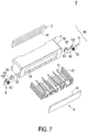
- FIG. 7 is a schematic exploded view illustrating the package assembly of FIG. 6 .
- Component parts and elements of the package assembly 8 of this example corresponding to those of the first embodiment are designated by identical numeral references, and detailed descriptions thereof are omitted.
- the main body 80 of the package assembly 8 of this example is not equipped with the housing base 7. That is, the main body 80 of the package assembly 8 only comprises the housing frame 5 and the two mounting brackets 6.
- the power module 4 is disposed within the first channel 51 of the housing frame 5 to cover the first channel 51.
- the hollow part 20 of the main body 80 is defined by the first channel 51.
- the second fixing part 61 of the mounting bracket 6 of this example is not accommodated within the first channel 51 but attached on an outer surface of the corresponding frame plate 50 of the housing frame 5.
- at least one second mounting hole 52 is formed in the outer surface of the corresponding frame plate 50 of the housing frame 5, and at least one third mounting hole 63 corresponding to the at least one second mounting hole 52 is formed in the second fixing part 61 of the mounting bracket 6.
- a screw 100 is penetrated through the corresponding third mounting hole 63 and the corresponding second mounting hole 52 so as to securely fix the second fixing part 61 on the outer surface of the corresponding frame plate 50 of the housing frame 5 and disposed outside the housing frame 5.
- a bottom surface of the first fixing part 60 is substantially coplanar with a bottom surface of the corresponding frame plate 50 of the housing frame 5.
- FIG. 8 is a schematic perspective view illustrating a package assembly according to a further example not forming part of of the present invention.
- FIG. 9 is a schematic exploded view illustrating the package assembly of FIG. 8 . Please refer to FIGS. 8 and 9 .
- the main body 90 of the package assembly 9 of this example is not equipped with the housing base 7, and only comprises the housing frame 5 and the two mounting brackets 6.
- Component parts and elements of the package assembly 9 of this example corresponding to those of the previous example are designated by identical numeral references, and detailed descriptions thereof are omitted.
- At least one receiving recess 54 is formed in the bottom surface of the corresponding frame plate 50 of the package assembly 9 of this embodiment, and at least one second mounting hole 52 is formed in the corresponding receiving recess 54.
- the mounting bracket 6 of this example only comprises the first fixing part 60, but the second fixing part 61 is omitted.
- the first fixing part 60 comprises the at least one first mounting hole 62 and further comprises at least one fourth mounting hole 64 corresponding to the at least one second mounting hole 52.
- a first end of the first fixing part 60 is locked into the corresponding receiving recess 54.
- a screw 100 is penetrated through the corresponding fourth mounting hole 64 and the corresponding second mounting hole 52 so as to securely fix the first fixing part 60 in the receiving recess 54.
- a bottom surface of the first fixing part 60 is substantially coplanar with a bottom surface of the corresponding frame plate 50 of the housing frame 5.
- the fourth mounting hole 64 is formed in the first end of the first fixing part 60
- the first mounting hole 62 is formed in the second end of the first fixing part 60.
- the present invention provides a package assembly as defined in claim 1.
- the package assembly comprises a main body, a power module and a replaceable top cover.
- the first pins of the power module can be penetrated through the corresponding first openings of the top cover.
- the top cover is selected according to the positions, number and size of the first pins of the power module. Since the first pins are penetrated through the corresponding first openings, the first pins may be electrically connected with the external circuit. Consequently, the utilization flexibility of the package assembly is enhanced. In the conventional technology, it is necessary to rebuild the mold of the non-plate cover or the non-plate package shell according to the number and positions of the pins of the power module. Since the top cover of the package assembly of the present invention is replaceable, the fabricating cost of the package assembly is largely reduced.
Landscapes
- Engineering & Computer Science (AREA)
- Power Engineering (AREA)
- Casings For Electric Apparatus (AREA)
- Microelectronics & Electronic Packaging (AREA)
- Non-Portable Lighting Devices Or Systems Thereof (AREA)
Description
- The present invention relates to a package assembly, and more particularly to a package assembly with a replaceable top cover for allowing pins of a power module to be penetrated through.
- Recently, the general trends in designing electronic devices are toward small size, light weightiness and easy portability. Moreover, with the increasing development of electronic industries, the internal circuitries of the electronic devices are gradually modularized. In other words, plural electronic components are integrated into a single circuit module. For example, a power module is one of the widely-used circuit modules. An example of the power module includes but is not limited to a DC-to-DC converter, a DC-to-AC converter or an AC-to-DC converter. After the electronic components (e.g. capacitors, resistors, inductors, transformers, diodes and transistors) are integrated as a power module, the power module may be installed on a system circuit board.
- A conventional package structure of a power module will be illustrated as follows. Firstly, plural power semiconductor bare chips, plural passive components and plural pins are disposed on a substrate. Through the pins, the power module can be connected with an external circuitry. In particular, the power semiconductor bare chips, the passive components and the pins are welded on the substrate via solder paste. Then, the power semiconductor bare chips, the passive components and the pins are connected with each other through conductive wires by a wire bonding process. Consequently, an exposed power module is produced. Moreover, the power semiconductor bare chips, the passive components and the pins of the exposed power module are covered by an inverted U-shaped covering member. The covering member has plural openings corresponding to the pins. The pins are penetrated through the corresponding pins and partially exposed outside the covering member. Meanwhile, the package structure of the power module is produced. Moreover, the exposed pins may be inserted into corresponding insertion holes of a printed circuit board.
US 4 515 587 A1 A high power semiconductor package which includes a substantially continuous mounting surface for efficient thermal mounting to a heat sink and which can be electrically isolated or non-isolated. The package includes a metal header having a cylindrical section and a peripheral mounting flange. The cylindrical section has an annular portion adjacent to the mounting flange into which is press fitted a thermally conductive disk having an outer surface which is substantially coplanar with the mounting surface of the flange. One or more semiconductor devices are mounted within the cylindrical section in thermal communication with the conductive disk, and are electrically connected to leads which outwardly extend from the top of the header. An encapsulant can be provided within the header to enclose the semiconductor devices, and an electrically insulating cap can be secured to the cylindrical section and through which the leads extend.
US 4 387 388 A1 discloses a connector assembly for connection to a computer backpanel or the like includes a leadless integrated circuit package and a connector receptacle for receiving the leadless package. The leadless package has two insulating layers and outwardly extending conductors formed on each of the two layers. The insulating layers have contact coupling edges, with the contact coupling edge of one layer extending outwardly of the contact coupling edge of the other layer. Rows of contacts in the receptacle make electrical contact with the conductors on the leadless package at the contact coupling edges. In a second embodiment, the connector assembly includes a leadless integrated circuit package having three insulating layers and outwardly extending conductors formed on each of the three layers. - However, the above package structure of the power module still has some drawbacks. For example, since the number and positions of the openings of the covering member are fixed, the covering member is only applied to a specified power module with the fit pin number and pin positions. That is, the utilization flexibility is not satisfactory. If the number and positions of the pins of the power module cannot fit the covering member, the covering member cannot be used for the power module. Under this circumstance, it is necessary to rebuild the new covering member. Consequently, the fabricating cost is increased.
- For solving the above drawbacks, another package assembly of the power module was disclosed. The package assembly comprises a non-plate package shell and a power module. Similarly, the power module is an exposed power module. The power module is completely covered by the package shell. The package shell has plural openings in a matrix configuration (e.g., in an M×N matrix configuration). The pins of the power module are penetrated through corresponding openings of the package shell. Since the openings of the package shell are arranged in the matrix configuration, the package shell can be applied to many types of power modules with different pin numbers or pin positions. Under this circumstance, the utilization flexibility is enhanced.
- However, if the positions, number and size of the pins of the power module cannot fit the openings of the package shell, the applications of the above package assembly are restricted. In other words, the package shell cannot be applied to all types of power modules. That is, if the positions, number and size of the pins of the power module cannot fit the openings of the package shell, it is necessary to rebuild the new package shell. Consequently, the fabricating cost is increased. Recently, the power module is packaged as an embedded power module. That is, the active component(s) and/or the passive component(s) are embedded within the substrate, and the pins are disposed on the surface of the substrate at the positions corresponding to the active component(s) and/or the passive component(s). Since the number and positions of the active component(s) and/or the passive component(s) embedded within the substrate are diversified, the positions, number and size of the pins are also diversified. In other words, the applications of the above package assembly to the embedded power module are largely reduced.
- Therefore, there is a need of providing an improved package assembly in order to eliminate the above drawbacks.
- The present invention provides a package assembly. assembly as defined in
claim 1. The package assembly comprises a main body, a power module and a replaceable top cover. The pins of the power module can be penetrated through the corresponding openings of the top cover. The top cover is selected according to the positions, number and size of the pins of the power module. Consequently, the utilization flexibility of the package assembly is largely enhanced and the fabricating cost is reduced. More especially, the package assembly can be applied to the embedded power module. - The above contents of the present invention will become more readily apparent to those ordinarily skilled in the art after reviewing the following detailed description and accompanying drawings, in which:
-
-
FIG. 1 is a schematic perspective view illustrating a package assembly according to a first embodiment of the present invention; -
FIG. 2 is a schematic exploded view illustrating the package assembly according to the first embodiment of the present invention; -
FIG. 3 is a schematic cutaway view illustrating the package assembly ofFIG. 1 and taken along the line A-A; -
FIG. 4A is a schematic top view illustrating the top cover of the package assembly according to the first embodiment of the present invention; -
FIG. 4B is a schematic top view illustrating a variant example of the top cover ofFIG. 4A ; -
FIG. 5A is a schematic perspective view illustrating the mounting bracket of the package assembly according to the first embodiment of the present invention; -
FIG. 5B is a schematic perspective view illustrating a variant example of the mounting bracket ofFIG. 5A ; -
FIG. 6 is a schematic perspective view illustrating a package assembly according to an example not forming part of the present invention; -
FIG. 7 is a schematic exploded view illustrating the package assembly according toFig. 6 ; -
FIG. 8 is a schematic perspective view illustrating a package assembly according to a further example not forming part of the present invention; and -
FIG. 9 is a schematic exploded view illustrating the package assembly according to the example according toFig. 8 . - The present invention will now be described more specifically with reference to the following embodiments. It is to be noted that the following descriptions of preferred embodiments of this invention are presented herein for purpose of illustration and description only. It is not intended to be exhaustive or to be limited to the precise form disclosed.
-
FIG 1 is a schematic perspective view illustrating a package assembly according to a first embodiment of the present invention.FIG. 2 is a schematic exploded view illustrating the package assembly ofFIG. 1 .FIG. 3 is a schematic cutaway view illustrating the package assembly ofFIG. 1 and taken along the line A-A. Please refer toFIGS. 1 ,2 and3 . Thepackage assembly 1 comprises amain body 2, atop cover 3 and apower module 4. Themain body 2 is substantially a rectangular box with ahollow part 20. Thehollow part 20 runs through a top part and a bottom part of themain body 2. - The
power module 4 is disposed within thehollow part 20 of themain body 2 and located beside the bottom part of themain body 2. Moreover, a second open end of thehollow part 20 near the bottom part of themain body 2 is covered by thepower module 4. Moreover, at least onefirst pin 41 is disposed on asurface 40 of thepower module 4. In particular, the at least onefirst pin 41 is disposed on a middle region of thesurface 40 of thepower module 4. When the second open end of thehollow part 20 near the bottom part of themain body 2 is covered by thepower module 4, the at least onefirst pin 41 is accommodated within thehollow part 20 of themain body 2 and partially protruded out of a first open end of thehollow part 20 near the top part of themain body 2. - In some embodiments, the at least one
first pin 41 is welded on thesurface 40 of thepower module 4. An example of thepower module 4 includes but is not limited to an embedded power module. That is, thepower module 4 comprises a substrate, one or more active components and/or one or more passive components, wherein the active components and/or the passive components are embedded within the substrate and electrically connected with the at least onefirst pin 41. Moreover, thepower module 4 may be fixed on the bottom part of themain body 2 by an adhesive or a locking means. - The
top cover 3 is a flat covering plate, which is disposed within thehollow part 20 for covering the first open end of thehollow part 20. Thetop cover 3 is abutted against a portion of themain body 2, so that thetop cover 3 and themain body 2 are combined together. Moreover, thetop cover 3 comprises at least onehole 30 corresponding to the at least onefirst pin 41 of thepower module 4. As shown inFIG. 1 , thetop cover 3 comprises pluralfirst openings 30. Thefirst openings 30 are aligned with corresponding first pins 41 of thepower module 4. When the first open end of thehollow part 20 is covered by thetop cover 3, thefirst pins 41 of thepower module 4 are penetrated through the correspondingfirst openings 30 of thetop cover 3. Consequently, thefirst pins 41 are partially exposed outside thehollow part 20 of themain body 2 and thetop cover 3, and located at the external portion of thepackage assembly 1. In this embodiment, the size of thetop cover 3 fits the size of the first open end of thehollow part 20. -
FIG. 4A is a schematic top view illustrating the top cover of the package assembly ofFIG. 1 .FIG. 4B is a schematic top view illustrating a variant example of the top cover ofFIG. 4A . In some embodiments, the pluralfirst openings 30 of thetop cover 3 are arranged in a matrix configuration. As shown inFIG. 4A , the pluralfirst openings 30 of thetop cover 3 are arranged in a 1 0x 12 matrix configuration. As shown inFIG. 4B , the pluralfirst openings 30 of thetop cover 3 are arranged in an 8×10 matrix configuration. Thefirst openings 30 as shown inFIG. 4A are smaller than thefirst openings 30 as shown inFIG. 4B . It is noted that the positions, number and size of thefirst openings 30 of thetop cover 3 are not restricted. Moreover, the positions, number and size of thefirst openings 30 may be determined according to the positions, number and size of thefirst pins 41 of thepower module 4. For example, thetop cover 3 may comprise one or pluralfirst openings 30. Alternatively, the pluralfirst openings 30 may be arranged in an irregular configuration. - In accordance with a feature of the present invention, the
top cover 3 of thepackage assembly 1 is replaceable. According to the positions, number and size of thefirst pins 41 of thepower module 4, thetop cover 3 with thefirst openings 30 corresponding to the first pins 41 is selected. Consequently, thefirst pins 41 of thepower module 4 can be penetrated through the correspondingfirst openings 30, wherein thefirst pins 41 are partially exposed outside thehollow part 20 of themain body 2 and thetop cover 3 and located at the external portion of thepackage assembly 1. Moreover, since thefirst pins 41 are exposed outside thehollow part 20 of themain body 2 and thetop cover 3, thefirst pins 41 may be inserted into corresponding insertion holes of an external circuit (e.g., a printed circuit board) and electrically connected with the external circuit. Since thetop cover 3 of thepackage assembly 1 is replaceable, the utilization flexibility of thepackage assembly 1 is enhanced. Since thetop cover 3 is selected according to thefirst pins 4 of thepower module 4, thepackage assembly 1 can have diversified variant examples by providingdifferent power module 4 with different first pin topologies and providing the fittop cover 3. As previously described, the conventional technology has to rebuild the mold of the non-plate cover or the non-plate package shell according to the number and positions of the pins of the power module. Since thetop cover 3 of thepackage assembly 1 of the present invention is replaceable, the fabricating cost of thepackage assembly 1 is largely reduced. - Please refer to
FIGS. 1 and2 again. In some embodiments, at least onesecond pin 42 is disposed on thesurface 40 of thepower module 4. In particular, the at least onesecond pin 42 is disposed on a periphery region of thesurface 40 of thepower module 4. Moreover, themain body 2 further comprises plural sidewalls. At least onesecond opening 21 corresponding to the at least onesecond pin 42 is formed in at least one sidewall of themain body 2. In this embodiment, pluralsecond openings 21 run through the top part of themain body 2, and thepower module 4 comprises plural second pins 42. When the second open end of thehollow part 20 near the bottom part of themain body 2 is covered by thepower module 4, thesecond pins 42 are accommodated within thehollow part 20 of themain body 2 and penetrated through the correspondingsecond openings 21, and partially protruded out of the top part of themain body 2. - In some embodiments, the
package assembly 1 further comprises a heat sink (not shown). In particular, the heat sink is attached on thepower module 4 of thepackage assembly 1. During the operations of thepower module 4, the heat generated by thepower module 4 may be transferred to the surroundings through the heat sink. Due to the heat sink, the heat dissipating efficiency is enhanced. In this embodiment, themain body 2 of thepackage assembly 1 comprises ahousing frame 5, at least one mountingbracket 6 and a housing base 7. Thehousing frame 5 is a rectangular hollow box. Moreover, thehousing frame 5 comprisesplural frame plates 50, afirst channel 51 and at least one receivingrecess 53. Theplural frame plates 50 constitute the plural sidewalls of themain body 2. The bilateral sides of eachframe plate 50 are connected with twoadjacent frame plates 50, respectively. Thefirst channel 51 is defined by theplural frame plates 50. The mountingbracket 6 comprises a first fixingpart 60 and a second fixingpart 61. A first end of the first fixingpart 60 is connected with and perpendicular to the second fixingpart 61. Consequently, the mountingbracket 6 is an L-shaped bracket. Thesecond fixing part 61 is accommodated within thefirst channel 51. The first end of the first fixingpart 60 is locked into the corresponding receivingrecess 53, and a second end of the first fixingpart 60 is exposed outside thepackage assembly 1. Moreover, the second end of the first fixingpart 60 has at least one mountinghole 62. After a screw (not shown) is penetrated through the mountinghole 62 and tightened into the heat sink, thepackage assembly 1 can be fixed on the heat sink. - In this embodiment, the housing base 7 is a stepped structure with a
first base part 70, asecond base part 71 and asecond channel 72. The housing base 7 is combined with thehousing frame 5. In particular, thefirst base part 70 is accommodated within thefirst channel 51, so that the second fixingpart 61 of each mountingbracket 6 is clamped between thefirst base part 70 and thehousing frame 5. Since the second fixingpart 61 is clamped between thefirst base part 70 and thehousing frame 5, the second fixingpart 61 is fixed in thefirst channel 51. Moreover, thesecond base part 71 is connected with thefirst base part 70. The size of thesecond base part 71 is larger than the size of thefirst channel 51. Consequently, when thefirst base part 70 is accommodated within thefirst channel 51, thesecond base part 71 is in contact with the bottom surfaces of theplural frame plates 50. Moreover, thesecond channel 72 runs through thefirst base part 70 and thesecond base part 71. Thepower module 4 is accommodated within thesecond channel 72 to cover thesecond channel 72. Moreover, when the housing base 7 and thehousing frame 5 are combined together, thefirst channel 51 and thesecond channel 72 are in communication with each other to define thehollow part 20 of themain body 2. -
FIG. 5A is a schematic perspective view illustrating the mounting bracket of the package assembly ofFIG. 1 .FIG. 5B is a schematic perspective view illustrating a variant example of the mounting bracket ofFIG. 5A . As shown inFIG. 5A , the first fixingpart 60 of the mountingbracket 6 comprises three mountingholes 62. For complying with different types of screws, one of the three mountingholes 62 is a circular hole, and the other two of the three mountingholes 62 are arc-shaped holes of different sizes. As shown inFIG. 5B , the three mountingholes 62 are a circular hole, an arc-shaped hole and a composite square and arc-shaped hole. -
FIG. 6 is a schematic perspective view illustrating a package assembly according to an example not forming part of of the present invention.FIG. 7 is a schematic exploded view illustrating the package assembly ofFIG. 6 . Please refer toFIGS. 6 and7 . Component parts and elements of thepackage assembly 8 of this example corresponding to those of the first embodiment are designated by identical numeral references, and detailed descriptions thereof are omitted. In comparison with thepackage assembly 1 of the first embodiment, themain body 80 of thepackage assembly 8 of this example is not equipped with the housing base 7. That is, themain body 80 of thepackage assembly 8 only comprises thehousing frame 5 and the two mountingbrackets 6. Moreover, thepower module 4 is disposed within thefirst channel 51 of thehousing frame 5 to cover thefirst channel 51. In this example, thehollow part 20 of themain body 80 is defined by thefirst channel 51. In comparison with the first embodiment, the second fixingpart 61 of the mountingbracket 6 of this example is not accommodated within thefirst channel 51 but attached on an outer surface of thecorresponding frame plate 50 of thehousing frame 5. Moreover, at least one second mountinghole 52 is formed in the outer surface of thecorresponding frame plate 50 of thehousing frame 5, and at least one third mountinghole 63 corresponding to the at least one second mountinghole 52 is formed in the second fixingpart 61 of the mountingbracket 6. After the second fixingpart 61 is attached on the outer surface of thecorresponding frame plate 50 of thehousing frame 5, ascrew 100 is penetrated through the corresponding third mountinghole 63 and the corresponding second mountinghole 52 so as to securely fix the second fixingpart 61 on the outer surface of thecorresponding frame plate 50 of thehousing frame 5 and disposed outside thehousing frame 5. Moreover, a bottom surface of the first fixingpart 60 is substantially coplanar with a bottom surface of thecorresponding frame plate 50 of thehousing frame 5. -
FIG. 8 is a schematic perspective view illustrating a package assembly according to a further example not forming part of of the present invention.FIG. 9 is a schematic exploded view illustrating the package assembly ofFIG. 8 . Please refer toFIGS. 8 and9 . Similarly, themain body 90 of thepackage assembly 9 of this example is not equipped with the housing base 7, and only comprises thehousing frame 5 and the two mountingbrackets 6. Component parts and elements of thepackage assembly 9 of this example corresponding to those of the previous example are designated by identical numeral references, and detailed descriptions thereof are omitted. In comparison with thepackage assembly 8 of the previous example, at least one receivingrecess 54 is formed in the bottom surface of thecorresponding frame plate 50 of thepackage assembly 9 of this embodiment, and at least one second mountinghole 52 is formed in the corresponding receivingrecess 54. Moreover, the mountingbracket 6 of this example only comprises the first fixingpart 60, but the second fixingpart 61 is omitted. The first fixingpart 60 comprises the at least one first mountinghole 62 and further comprises at least one fourth mountinghole 64 corresponding to the at least one second mountinghole 52. Moreover, a first end of the first fixingpart 60 is locked into the corresponding receivingrecess 54. When the first end of the first fixingpart 60 is locked into the corresponding receivingrecess 54, ascrew 100 is penetrated through the corresponding fourth mountinghole 64 and the corresponding second mountinghole 52 so as to securely fix the first fixingpart 60 in the receivingrecess 54. Moreover, a bottom surface of the first fixingpart 60 is substantially coplanar with a bottom surface of thecorresponding frame plate 50 of thehousing frame 5. In this example, the fourth mountinghole 64 is formed in the first end of the first fixingpart 60, and the first mountinghole 62 is formed in the second end of the first fixingpart 60. - From the above descriptions, the present invention provides a package assembly as defined in
claim 1. The package assembly comprises a main body, a power module and a replaceable top cover. The first pins of the power module can be penetrated through the corresponding first openings of the top cover. The top cover is selected according to the positions, number and size of the first pins of the power module. Since the first pins are penetrated through the corresponding first openings, the first pins may be electrically connected with the external circuit. Consequently, the utilization flexibility of the package assembly is enhanced. In the conventional technology, it is necessary to rebuild the mold of the non-plate cover or the non-plate package shell according to the number and positions of the pins of the power module. Since the top cover of the package assembly of the present invention is replaceable, the fabricating cost of the package assembly is largely reduced.
Claims (8)
- A package assembly (1, 8, 9), comprising:a main body (2, 80, 90) having a hollow part (20), wherein the hollow part (20) runs through a top part and a bottom part of the main body (2, 80, 90) wherein the main body (2, 80, 90) further comprises a housing frame (5) and a mounting bracket (6), the housing frame (5) comprises plural frame plates (50), a first channel (51) and a receiving recess (53), and the mounting bracket (6) comprises a first fixing part (60) and a second fixing part (61), wherein the first channel (51) is defined by the plural frame plates (50), the second fixing part (61) is accommodated within the first channel (51), a first end of the first fixing part (60) is locked into the receiving recess (53), and a second end of the first fixing part (60) is exposed outside the package assembly (1) and has at least one first mounting hole (62);a power module (4) disposed within the hollow part (20) of the main body (2, 80, 90) and located beside the bottom part of the main body (2, 80, 90), wherein at least one first pin (41) is disposed on a surface (40) of the power module (4), and the at least one first pin (41) is accommodated within the hollow part (20) of the main body (2, 80, 90) and partially protruded out of a first open end of the hollow part (20) near the top part of the main body (2, 80, 90); anda replaceable top cover (3) disposed in the hollow part (20) of the main body (2, 80, 90), and comprising at least one first opening (30) corresponding to the at least one first pin (41), wherein the at least one first pin (41) is penetrated through the corresponding first opening (30) and exposed outside the first open end of the hollow part (20).
- The package assembly according to claim 1, wherein the power module comprises a plurality of electronic components embedded within a dielectric substrate.
- The package assembly according to claim 1 or 2, wherein a second open end of the hollow part (20) near the bottom part of the main body (2, 80, 90) is covered by the power module (4).
- The package assembly according to any oft he claims 1 to 3, wherein the top cover is a flat covering plate comprising plural first openings (30) arranged in a matrix configuration.
- The package assembly according to any of the claims 1 to 4, wherein the at least one first pin (30) is disposed on a middle region of the surface (40) of the power module (4) and at least one second pin (42) is disposed on a periphery region of the surface (40) of the power module (4).
- The package assembly according to claim 5, wherein the main body (2, 80, 90) further comprises at least one second opening (21) corresponding to the at least one second pin (42), and the at least one second opening (21) runs through the top part of the main body (2, 80, 90), wherein the at least one second pin (42) is accommodated within the hollow part (20) of the main body (2, 80, 90) and partially protruded out of the top part of the main body (2, 80, 90).
- The package assembly according to any of the claims 1-6, wherein the first end of the first fixing part (60) is connected with and perpendicular to the second fixing part (61), so that the mounting bracket (6) is an L-shaped bracket.
- The package assembly according to any of the claims 1 to 7, wherein the main body (2) further comprises a housing base (7), and the housing base (7) is combined with the housing frame (5), wherein the housing base (7) comprises:a first base part (70) accommodated within the first channel (51), wherein the second fixing part (61) is clamped between the first base part (70) and the housing frame (5), so that the second fixing part (61) is fixed in the first channel (51);a second base part (71) connected with the first base part (70), wherein the second base part (71) is in contact with a bottom surface of the housing frame (5); anda second channel (72) running through the first base part (70) and the second base part (71), wherein the power module (4) is accommodated within the second channel (72) to cover the second channel (72),
wherein when the housing base (7) and the housing frame (5) are combined together, the first channel (51) and the second channel (72) are in communication with each other to define the hollow part (20) of the main body (2).
Applications Claiming Priority (1)
| Application Number | Priority Date | Filing Date | Title |
|---|---|---|---|
| SG10201504274SA SG10201504274SA (en) | 2015-05-29 | 2015-05-29 | Package assembly |
Publications (3)
| Publication Number | Publication Date |
|---|---|
| EP3098843A1 EP3098843A1 (en) | 2016-11-30 |
| EP3098843B1 true EP3098843B1 (en) | 2019-10-02 |
| EP3098843B8 EP3098843B8 (en) | 2020-03-04 |
Family
ID=57399259
Family Applications (1)
| Application Number | Title | Priority Date | Filing Date |
|---|---|---|---|
| EP16171766.5A Active EP3098843B8 (en) | 2015-05-29 | 2016-05-27 | Package assembly |
Country Status (4)
| Country | Link |
|---|---|
| US (1) | US9906157B2 (en) |
| EP (1) | EP3098843B8 (en) |
| CN (1) | CN106206523A (en) |
| SG (1) | SG10201504274SA (en) |
Cited By (1)
| Publication number | Priority date | Publication date | Assignee | Title |
|---|---|---|---|---|
| US12628650B2 (en) | 2022-09-22 | 2026-05-12 | Industrial Technology Research Institute | Mounting structure and module device having the same |
Families Citing this family (7)
| Publication number | Priority date | Publication date | Assignee | Title |
|---|---|---|---|---|
| US10522945B2 (en) | 2016-08-22 | 2019-12-31 | Interplex Industries, Inc. | Electrical connector |
| MX389531B (en) * | 2016-08-22 | 2025-03-20 | Interplex Ind Inc | ELECTRICAL CONNECTOR. |
| WO2022163788A1 (en) * | 2021-01-29 | 2022-08-04 | 京セラ株式会社 | Semiconductor package and semiconductor electronic device |
| US12513870B2 (en) * | 2021-07-22 | 2025-12-30 | Semiconductor Components Industries, Llc | Power module |
| DE102022103471A1 (en) * | 2022-02-15 | 2023-08-17 | Audi Aktiengesellschaft | Electrical switching device, electrical drive device and motor vehicle |
| CN114975289B (en) * | 2022-06-02 | 2023-06-27 | 上海晶岳电子有限公司 | A vdmos device |
| TWD231825S (en) | 2023-06-29 | 2024-06-21 | 財團法人工業技術研究院 新竹縣竹東鎮中興路四段195號 (中華民國) | Housing of power module |
Citations (1)
| Publication number | Priority date | Publication date | Assignee | Title |
|---|---|---|---|---|
| FR2500959A1 (en) * | 1981-02-27 | 1982-09-03 | Thomson Csf | ELECTRONIC DEVICE HOUSING WITH HIGH THERMAL DISSIPATION |
Family Cites Families (23)
| Publication number | Priority date | Publication date | Assignee | Title |
|---|---|---|---|---|
| US4387388A (en) | 1980-07-14 | 1983-06-07 | Ncr Corporation | Package and connector receptacle |
| US4514587A (en) | 1981-12-23 | 1985-04-30 | Unitrode Corporation | High power semiconductor package |
| DE3604882A1 (en) | 1986-02-15 | 1987-08-20 | Bbc Brown Boveri & Cie | PERFORMANCE SEMICONDUCTOR MODULE AND METHOD FOR PRODUCING THE MODULE |
| JPS6370444A (en) * | 1986-09-12 | 1988-03-30 | Hitachi Ltd | electronic equipment |
| US7477518B2 (en) * | 2004-09-06 | 2009-01-13 | Infineon Technologies Ag | Sub-assembly |
| DE102008005547B4 (en) * | 2008-01-23 | 2013-08-29 | Infineon Technologies Ag | Power semiconductor module and circuit arrangement with a power semiconductor module |
| DE102008007310B4 (en) * | 2008-02-02 | 2016-01-07 | Vincotech Holdings S.à.r.l. | Electrical press-fit contact |
| JP2010147116A (en) * | 2008-12-17 | 2010-07-01 | Mitsubishi Electric Corp | Semiconductor device |
| DE102009025113A1 (en) * | 2009-06-11 | 2010-12-16 | Continental Teves Ag & Co. Ohg | Press-in contact for connecting an electronic component to a printed circuit board and press-fit tool |
| WO2011083737A1 (en) * | 2010-01-05 | 2011-07-14 | 富士電機システムズ株式会社 | Unit for semiconductor device, and semiconductor device |
| JP2012005301A (en) * | 2010-06-18 | 2012-01-05 | Fuji Electric Co Ltd | Power semiconductor module |
| DE112012002122B4 (en) * | 2011-05-17 | 2020-11-26 | Interplex Industries, Inc. | Inter-plate connection system with deformation avoidance of flexible flexible pins |
| JP5454646B1 (en) * | 2012-09-25 | 2014-03-26 | 第一精工株式会社 | Electrical connector |
| CN104919657B (en) * | 2013-01-14 | 2019-05-10 | 威世通用半导体公司 | Voltage distribution pins for semiconductor modules |
| JP6119313B2 (en) * | 2013-03-08 | 2017-04-26 | 富士電機株式会社 | Semiconductor device |
| KR101477378B1 (en) * | 2013-03-21 | 2014-12-29 | 삼성전기주식회사 | Housing and power module having the same |
| JP6171586B2 (en) | 2013-06-04 | 2017-08-02 | 富士電機株式会社 | Semiconductor device |
| US9967986B2 (en) * | 2014-01-02 | 2018-05-08 | Semiconductor Components Industries, Llc | Semiconductor package and method therefor |
| US9620877B2 (en) * | 2014-06-17 | 2017-04-11 | Semiconductor Components Industries, Llc | Flexible press fit pins for semiconductor packages and related methods |
| TWI557857B (en) * | 2015-01-22 | 2016-11-11 | 台達電子工業股份有限公司 | Package structure of power module |
| US20160240452A1 (en) * | 2015-02-18 | 2016-08-18 | Semiconductor Components Industries, Llc | Semiconductor packages with sub-terminals and related methods |
| US9431311B1 (en) * | 2015-02-19 | 2016-08-30 | Semiconductor Components Industries, Llc | Semiconductor package with elastic coupler and related methods |
| US10825748B2 (en) * | 2015-12-15 | 2020-11-03 | Semiconductor Components Industries, Llc | Semiconductor package system and related methods |
-
2015
- 2015-05-29 SG SG10201504274SA patent/SG10201504274SA/en unknown
-
2016
- 2016-05-26 US US15/165,719 patent/US9906157B2/en active Active
- 2016-05-27 EP EP16171766.5A patent/EP3098843B8/en active Active
- 2016-05-27 CN CN201610366271.8A patent/CN106206523A/en active Pending
Patent Citations (1)
| Publication number | Priority date | Publication date | Assignee | Title |
|---|---|---|---|---|
| FR2500959A1 (en) * | 1981-02-27 | 1982-09-03 | Thomson Csf | ELECTRONIC DEVICE HOUSING WITH HIGH THERMAL DISSIPATION |
Cited By (1)
| Publication number | Priority date | Publication date | Assignee | Title |
|---|---|---|---|---|
| US12628650B2 (en) | 2022-09-22 | 2026-05-12 | Industrial Technology Research Institute | Mounting structure and module device having the same |
Also Published As
| Publication number | Publication date |
|---|---|
| US9906157B2 (en) | 2018-02-27 |
| CN106206523A (en) | 2016-12-07 |
| EP3098843A1 (en) | 2016-11-30 |
| US20160352245A1 (en) | 2016-12-01 |
| EP3098843B8 (en) | 2020-03-04 |
| SG10201504274SA (en) | 2016-12-29 |
Similar Documents
| Publication | Publication Date | Title |
|---|---|---|
| US9906157B2 (en) | Package assembly | |
| US10685895B2 (en) | Power module with lead component and manufacturing method thereof | |
| US9698507B2 (en) | Package structure of power module | |
| US9425131B2 (en) | Package structure | |
| US20200152557A1 (en) | Package structure and packaging process | |
| US10892205B2 (en) | Package structure and power module using same | |
| EP3252812B1 (en) | Embedded package structure | |
| US8570745B2 (en) | Electrical connector assembly | |
| EP3098845B1 (en) | Package assembly | |
| US9633919B2 (en) | Package structure with an elastomer with lower elastic modulus | |
| US20180061570A1 (en) | Capacitor with improved heat dissipation | |
| US11114946B2 (en) | Voltage regulator module | |
| EP4044228B1 (en) | Power structure, preparation method, and device | |
| US20190043799A1 (en) | Package structure and fabricating method thereof | |
| CN104066290A (en) | Housing And Power Module Having The Same | |
| US7983046B1 (en) | Electronic control module and enclosed power module | |
| US8979575B2 (en) | Electrical connector assembly having assistant heat dissipating device | |
| KR102543495B1 (en) | PCB module having multi-directional heat-radiation structure, and radiation plate, multi-layer PCB assembly, and module case used in the same PCB module | |
| US20090237898A1 (en) | Heat sink arrangement for electrical apparatus | |
| US20190318974A1 (en) | Circuit module and method of manufacturing the same | |
| US20080036049A1 (en) | Stacked integration module and method for manufacturing the same | |
| EP3588557B1 (en) | Package structure | |
| US20050006758A1 (en) | Method for packaging electronic modules and multiple chip packaging | |
| EP3942905B1 (en) | Electrical apparatus comprising a power semiconductor module and at least one capacitor | |
| JPH0888299A (en) | Semiconductor device |
Legal Events
| Date | Code | Title | Description |
|---|---|---|---|
| PUAI | Public reference made under article 153(3) epc to a published international application that has entered the european phase |
Free format text: ORIGINAL CODE: 0009012 |
|
| STAA | Information on the status of an ep patent application or granted ep patent |
Free format text: STATUS: REQUEST FOR EXAMINATION WAS MADE |
|
| AK | Designated contracting states |
Kind code of ref document: A1 Designated state(s): AL AT BE BG CH CY CZ DE DK EE ES FI FR GB GR HR HU IE IS IT LI LT LU LV MC MK MT NL NO PL PT RO RS SE SI SK SM TR |
|
| AX | Request for extension of the european patent |
Extension state: BA ME |
|
| 17P | Request for examination filed |
Effective date: 20161111 |
|
| RBV | Designated contracting states (corrected) |
Designated state(s): AL AT BE BG CH CY CZ DE DK EE ES FI FR GB GR HR HU IE IS IT LI LT LU LV MC MK MT NL NO PL PT RO RS SE SI SK SM TR |
|
| STAA | Information on the status of an ep patent application or granted ep patent |
Free format text: STATUS: EXAMINATION IS IN PROGRESS |
|
| 17Q | First examination report despatched |
Effective date: 20181115 |
|
| REG | Reference to a national code |
Ref country code: DE Ref legal event code: R079 Ref document number: 602016021524 Country of ref document: DE Free format text: PREVIOUS MAIN CLASS: H01L0023040000 Ipc: H01L0023053000 |
|
| RIC1 | Information provided on ipc code assigned before grant |
Ipc: H01L 23/053 20060101AFI20190329BHEP |
|
| GRAP | Despatch of communication of intention to grant a patent |
Free format text: ORIGINAL CODE: EPIDOSNIGR1 |
|
| STAA | Information on the status of an ep patent application or granted ep patent |
Free format text: STATUS: GRANT OF PATENT IS INTENDED |
|
| INTG | Intention to grant announced |
Effective date: 20190531 |
|
| GRAS | Grant fee paid |
Free format text: ORIGINAL CODE: EPIDOSNIGR3 |
|
| GRAA | (expected) grant |
Free format text: ORIGINAL CODE: 0009210 |
|
| STAA | Information on the status of an ep patent application or granted ep patent |
Free format text: STATUS: THE PATENT HAS BEEN GRANTED |
|
| AK | Designated contracting states |
Kind code of ref document: B1 Designated state(s): AL AT BE BG CH CY CZ DE DK EE ES FI FR GB GR HR HU IE IS IT LI LT LU LV MC MK MT NL NO PL PT RO RS SE SI SK SM TR |
|
| REG | Reference to a national code |
Ref country code: GB Ref legal event code: FG4D |
|
| REG | Reference to a national code |
Ref country code: CH Ref legal event code: EP Ref country code: AT Ref legal event code: REF Ref document number: 1187120 Country of ref document: AT Kind code of ref document: T Effective date: 20191015 |
|
| REG | Reference to a national code |
Ref country code: DE Ref legal event code: R096 Ref document number: 602016021524 Country of ref document: DE |
|
| REG | Reference to a national code |
Ref country code: IE Ref legal event code: FG4D |
|
| GRAT | Correction requested after decision to grant or after decision to maintain patent in amended form |
Free format text: ORIGINAL CODE: EPIDOSNCDEC |
|
| REG | Reference to a national code |
Ref country code: CH Ref legal event code: PK Free format text: BERICHTIGUNG PRIORITAET |
|
| REG | Reference to a national code |
Ref country code: NL Ref legal event code: MP Effective date: 20191002 |
|
| REG | Reference to a national code |
Ref country code: LT Ref legal event code: MG4D |
|
| REG | Reference to a national code |
Ref country code: CH Ref legal event code: PK Free format text: BERICHTIGUNG B8 |
|
| REG | Reference to a national code |
Ref country code: AT Ref legal event code: MK05 Ref document number: 1187120 Country of ref document: AT Kind code of ref document: T Effective date: 20191002 |
|
| PG25 | Lapsed in a contracting state [announced via postgrant information from national office to epo] |
Ref country code: LT Free format text: LAPSE BECAUSE OF FAILURE TO SUBMIT A TRANSLATION OF THE DESCRIPTION OR TO PAY THE FEE WITHIN THE PRESCRIBED TIME-LIMIT Effective date: 20191002 Ref country code: GR Free format text: LAPSE BECAUSE OF FAILURE TO SUBMIT A TRANSLATION OF THE DESCRIPTION OR TO PAY THE FEE WITHIN THE PRESCRIBED TIME-LIMIT Effective date: 20200103 Ref country code: NL Free format text: LAPSE BECAUSE OF FAILURE TO SUBMIT A TRANSLATION OF THE DESCRIPTION OR TO PAY THE FEE WITHIN THE PRESCRIBED TIME-LIMIT Effective date: 20191002 Ref country code: PL Free format text: LAPSE BECAUSE OF FAILURE TO SUBMIT A TRANSLATION OF THE DESCRIPTION OR TO PAY THE FEE WITHIN THE PRESCRIBED TIME-LIMIT Effective date: 20191002 Ref country code: BG Free format text: LAPSE BECAUSE OF FAILURE TO SUBMIT A TRANSLATION OF THE DESCRIPTION OR TO PAY THE FEE WITHIN THE PRESCRIBED TIME-LIMIT Effective date: 20200102 Ref country code: FI Free format text: LAPSE BECAUSE OF FAILURE TO SUBMIT A TRANSLATION OF THE DESCRIPTION OR TO PAY THE FEE WITHIN THE PRESCRIBED TIME-LIMIT Effective date: 20191002 Ref country code: SE Free format text: LAPSE BECAUSE OF FAILURE TO SUBMIT A TRANSLATION OF THE DESCRIPTION OR TO PAY THE FEE WITHIN THE PRESCRIBED TIME-LIMIT Effective date: 20191002 Ref country code: LV Free format text: LAPSE BECAUSE OF FAILURE TO SUBMIT A TRANSLATION OF THE DESCRIPTION OR TO PAY THE FEE WITHIN THE PRESCRIBED TIME-LIMIT Effective date: 20191002 Ref country code: NO Free format text: LAPSE BECAUSE OF FAILURE TO SUBMIT A TRANSLATION OF THE DESCRIPTION OR TO PAY THE FEE WITHIN THE PRESCRIBED TIME-LIMIT Effective date: 20200102 Ref country code: PT Free format text: LAPSE BECAUSE OF FAILURE TO SUBMIT A TRANSLATION OF THE DESCRIPTION OR TO PAY THE FEE WITHIN THE PRESCRIBED TIME-LIMIT Effective date: 20200203 Ref country code: ES Free format text: LAPSE BECAUSE OF FAILURE TO SUBMIT A TRANSLATION OF THE DESCRIPTION OR TO PAY THE FEE WITHIN THE PRESCRIBED TIME-LIMIT Effective date: 20191002 Ref country code: AT Free format text: LAPSE BECAUSE OF FAILURE TO SUBMIT A TRANSLATION OF THE DESCRIPTION OR TO PAY THE FEE WITHIN THE PRESCRIBED TIME-LIMIT Effective date: 20191002 |
|
| PG25 | Lapsed in a contracting state [announced via postgrant information from national office to epo] |
Ref country code: IS Free format text: LAPSE BECAUSE OF FAILURE TO SUBMIT A TRANSLATION OF THE DESCRIPTION OR TO PAY THE FEE WITHIN THE PRESCRIBED TIME-LIMIT Effective date: 20200224 Ref country code: HR Free format text: LAPSE BECAUSE OF FAILURE TO SUBMIT A TRANSLATION OF THE DESCRIPTION OR TO PAY THE FEE WITHIN THE PRESCRIBED TIME-LIMIT Effective date: 20191002 Ref country code: CZ Free format text: LAPSE BECAUSE OF FAILURE TO SUBMIT A TRANSLATION OF THE DESCRIPTION OR TO PAY THE FEE WITHIN THE PRESCRIBED TIME-LIMIT Effective date: 20191002 Ref country code: RS Free format text: LAPSE BECAUSE OF FAILURE TO SUBMIT A TRANSLATION OF THE DESCRIPTION OR TO PAY THE FEE WITHIN THE PRESCRIBED TIME-LIMIT Effective date: 20191002 |
|
| PG25 | Lapsed in a contracting state [announced via postgrant information from national office to epo] |
Ref country code: AL Free format text: LAPSE BECAUSE OF FAILURE TO SUBMIT A TRANSLATION OF THE DESCRIPTION OR TO PAY THE FEE WITHIN THE PRESCRIBED TIME-LIMIT Effective date: 20191002 |
|
| REG | Reference to a national code |
Ref country code: DE Ref legal event code: R097 Ref document number: 602016021524 Country of ref document: DE |
|
| PG2D | Information on lapse in contracting state deleted |
Ref country code: IS |
|
| PG25 | Lapsed in a contracting state [announced via postgrant information from national office to epo] |
Ref country code: RO Free format text: LAPSE BECAUSE OF FAILURE TO SUBMIT A TRANSLATION OF THE DESCRIPTION OR TO PAY THE FEE WITHIN THE PRESCRIBED TIME-LIMIT Effective date: 20191002 Ref country code: DK Free format text: LAPSE BECAUSE OF FAILURE TO SUBMIT A TRANSLATION OF THE DESCRIPTION OR TO PAY THE FEE WITHIN THE PRESCRIBED TIME-LIMIT Effective date: 20191002 Ref country code: EE Free format text: LAPSE BECAUSE OF FAILURE TO SUBMIT A TRANSLATION OF THE DESCRIPTION OR TO PAY THE FEE WITHIN THE PRESCRIBED TIME-LIMIT Effective date: 20191002 Ref country code: IS Free format text: LAPSE BECAUSE OF FAILURE TO SUBMIT A TRANSLATION OF THE DESCRIPTION OR TO PAY THE FEE WITHIN THE PRESCRIBED TIME-LIMIT Effective date: 20200202 |
|
| PLBE | No opposition filed within time limit |
Free format text: ORIGINAL CODE: 0009261 |
|
| STAA | Information on the status of an ep patent application or granted ep patent |
Free format text: STATUS: NO OPPOSITION FILED WITHIN TIME LIMIT |
|
| PG25 | Lapsed in a contracting state [announced via postgrant information from national office to epo] |
Ref country code: IT Free format text: LAPSE BECAUSE OF FAILURE TO SUBMIT A TRANSLATION OF THE DESCRIPTION OR TO PAY THE FEE WITHIN THE PRESCRIBED TIME-LIMIT Effective date: 20191002 Ref country code: SM Free format text: LAPSE BECAUSE OF FAILURE TO SUBMIT A TRANSLATION OF THE DESCRIPTION OR TO PAY THE FEE WITHIN THE PRESCRIBED TIME-LIMIT Effective date: 20191002 Ref country code: SK Free format text: LAPSE BECAUSE OF FAILURE TO SUBMIT A TRANSLATION OF THE DESCRIPTION OR TO PAY THE FEE WITHIN THE PRESCRIBED TIME-LIMIT Effective date: 20191002 |
|
| 26N | No opposition filed |
Effective date: 20200703 |
|
| PG25 | Lapsed in a contracting state [announced via postgrant information from national office to epo] |
Ref country code: SI Free format text: LAPSE BECAUSE OF FAILURE TO SUBMIT A TRANSLATION OF THE DESCRIPTION OR TO PAY THE FEE WITHIN THE PRESCRIBED TIME-LIMIT Effective date: 20191002 |
|
| PG25 | Lapsed in a contracting state [announced via postgrant information from national office to epo] |
Ref country code: MC Free format text: LAPSE BECAUSE OF FAILURE TO SUBMIT A TRANSLATION OF THE DESCRIPTION OR TO PAY THE FEE WITHIN THE PRESCRIBED TIME-LIMIT Effective date: 20191002 Ref country code: CH Free format text: LAPSE BECAUSE OF NON-PAYMENT OF DUE FEES Effective date: 20200531 Ref country code: LI Free format text: LAPSE BECAUSE OF NON-PAYMENT OF DUE FEES Effective date: 20200531 |
|
| REG | Reference to a national code |
Ref country code: BE Ref legal event code: MM Effective date: 20200531 |
|
| GBPC | Gb: european patent ceased through non-payment of renewal fee |
Effective date: 20200527 |
|
| PG25 | Lapsed in a contracting state [announced via postgrant information from national office to epo] |
Ref country code: LU Free format text: LAPSE BECAUSE OF NON-PAYMENT OF DUE FEES Effective date: 20200527 |
|
| PG25 | Lapsed in a contracting state [announced via postgrant information from national office to epo] |
Ref country code: GB Free format text: LAPSE BECAUSE OF NON-PAYMENT OF DUE FEES Effective date: 20200527 Ref country code: IE Free format text: LAPSE BECAUSE OF NON-PAYMENT OF DUE FEES Effective date: 20200527 |
|
| PG25 | Lapsed in a contracting state [announced via postgrant information from national office to epo] |
Ref country code: BE Free format text: LAPSE BECAUSE OF NON-PAYMENT OF DUE FEES Effective date: 20200531 |
|
| PG25 | Lapsed in a contracting state [announced via postgrant information from national office to epo] |
Ref country code: TR Free format text: LAPSE BECAUSE OF FAILURE TO SUBMIT A TRANSLATION OF THE DESCRIPTION OR TO PAY THE FEE WITHIN THE PRESCRIBED TIME-LIMIT Effective date: 20191002 Ref country code: MT Free format text: LAPSE BECAUSE OF FAILURE TO SUBMIT A TRANSLATION OF THE DESCRIPTION OR TO PAY THE FEE WITHIN THE PRESCRIBED TIME-LIMIT Effective date: 20191002 Ref country code: CY Free format text: LAPSE BECAUSE OF FAILURE TO SUBMIT A TRANSLATION OF THE DESCRIPTION OR TO PAY THE FEE WITHIN THE PRESCRIBED TIME-LIMIT Effective date: 20191002 |
|
| PG25 | Lapsed in a contracting state [announced via postgrant information from national office to epo] |
Ref country code: MK Free format text: LAPSE BECAUSE OF FAILURE TO SUBMIT A TRANSLATION OF THE DESCRIPTION OR TO PAY THE FEE WITHIN THE PRESCRIBED TIME-LIMIT Effective date: 20191002 |
|
| REG | Reference to a national code |
Ref country code: FR Ref legal event code: PLFP Year of fee payment: 8 |
|
| PGFP | Annual fee paid to national office [announced via postgrant information from national office to epo] |
Ref country code: DE Payment date: 20250530 Year of fee payment: 10 |
|
| PGFP | Annual fee paid to national office [announced via postgrant information from national office to epo] |
Ref country code: FR Payment date: 20250530 Year of fee payment: 10 |
|
| REG | Reference to a national code |
Ref country code: DE Ref legal event code: R079 Ref document number: 602016021524 Country of ref document: DE Free format text: PREVIOUS MAIN CLASS: H01L0023053000 Ipc: H10W0076150000 |