EP3097844A1 - Optical scanning-type observing device - Google Patents
Optical scanning-type observing device Download PDFInfo
- Publication number
- EP3097844A1 EP3097844A1 EP15740622.4A EP15740622A EP3097844A1 EP 3097844 A1 EP3097844 A1 EP 3097844A1 EP 15740622 A EP15740622 A EP 15740622A EP 3097844 A1 EP3097844 A1 EP 3097844A1
- Authority
- EP
- European Patent Office
- Prior art keywords
- offset
- light emission
- light
- offset value
- tip
- Prior art date
- Legal status (The legal status is an assumption and is not a legal conclusion. Google has not performed a legal analysis and makes no representation as to the accuracy of the status listed.)
- Withdrawn
Links
- 230000003287 optical effect Effects 0.000 title claims abstract description 38
- 239000000835 fiber Substances 0.000 claims abstract description 24
- 238000012937 correction Methods 0.000 claims description 52
- 238000012545 processing Methods 0.000 claims description 25
- 230000002093 peripheral effect Effects 0.000 claims description 7
- 230000010355 oscillation Effects 0.000 claims description 3
- 239000013307 optical fiber Substances 0.000 description 39
- 238000005286 illumination Methods 0.000 description 32
- 238000003780 insertion Methods 0.000 description 14
- 230000037431 insertion Effects 0.000 description 14
- 238000001514 detection method Methods 0.000 description 13
- 238000010586 diagram Methods 0.000 description 10
- 239000003086 colorant Substances 0.000 description 7
- 230000000694 effects Effects 0.000 description 3
- 238000000034 method Methods 0.000 description 2
- 238000012986 modification Methods 0.000 description 2
- 230000004048 modification Effects 0.000 description 2
- 239000000523 sample Substances 0.000 description 2
- 238000005070 sampling Methods 0.000 description 2
- 0 COCC*1CCCC1 Chemical compound COCC*1CCCC1 0.000 description 1
- 206010027146 Melanoderma Diseases 0.000 description 1
- 238000006243 chemical reaction Methods 0.000 description 1
- 230000001360 synchronised effect Effects 0.000 description 1
Images



Classifications
-
- G—PHYSICS
- G02—OPTICS
- G02B—OPTICAL ELEMENTS, SYSTEMS OR APPARATUS
- G02B23/00—Telescopes, e.g. binoculars; Periscopes; Instruments for viewing the inside of hollow bodies; Viewfinders; Optical aiming or sighting devices
- G02B23/24—Instruments or systems for viewing the inside of hollow bodies, e.g. fibrescopes
- G02B23/2476—Non-optical details, e.g. housings, mountings, supports
- G02B23/2484—Arrangements in relation to a camera or imaging device
-
- A—HUMAN NECESSITIES
- A61—MEDICAL OR VETERINARY SCIENCE; HYGIENE
- A61B—DIAGNOSIS; SURGERY; IDENTIFICATION
- A61B1/00—Instruments for performing medical examinations of the interior of cavities or tubes of the body by visual or photographical inspection, e.g. endoscopes; Illuminating arrangements therefor
- A61B1/06—Instruments for performing medical examinations of the interior of cavities or tubes of the body by visual or photographical inspection, e.g. endoscopes; Illuminating arrangements therefor with illuminating arrangements
- A61B1/0655—Control therefor
-
- A—HUMAN NECESSITIES
- A61—MEDICAL OR VETERINARY SCIENCE; HYGIENE
- A61B—DIAGNOSIS; SURGERY; IDENTIFICATION
- A61B1/00—Instruments for performing medical examinations of the interior of cavities or tubes of the body by visual or photographical inspection, e.g. endoscopes; Illuminating arrangements therefor
- A61B1/00002—Operational features of endoscopes
- A61B1/00004—Operational features of endoscopes characterised by electronic signal processing
- A61B1/00006—Operational features of endoscopes characterised by electronic signal processing of control signals
-
- A—HUMAN NECESSITIES
- A61—MEDICAL OR VETERINARY SCIENCE; HYGIENE
- A61B—DIAGNOSIS; SURGERY; IDENTIFICATION
- A61B1/00—Instruments for performing medical examinations of the interior of cavities or tubes of the body by visual or photographical inspection, e.g. endoscopes; Illuminating arrangements therefor
- A61B1/00002—Operational features of endoscopes
- A61B1/00057—Operational features of endoscopes provided with means for testing or calibration
-
- A—HUMAN NECESSITIES
- A61—MEDICAL OR VETERINARY SCIENCE; HYGIENE
- A61B—DIAGNOSIS; SURGERY; IDENTIFICATION
- A61B1/00—Instruments for performing medical examinations of the interior of cavities or tubes of the body by visual or photographical inspection, e.g. endoscopes; Illuminating arrangements therefor
- A61B1/00163—Optical arrangements
- A61B1/00172—Optical arrangements with means for scanning
-
- A—HUMAN NECESSITIES
- A61—MEDICAL OR VETERINARY SCIENCE; HYGIENE
- A61B—DIAGNOSIS; SURGERY; IDENTIFICATION
- A61B1/00—Instruments for performing medical examinations of the interior of cavities or tubes of the body by visual or photographical inspection, e.g. endoscopes; Illuminating arrangements therefor
- A61B1/06—Instruments for performing medical examinations of the interior of cavities or tubes of the body by visual or photographical inspection, e.g. endoscopes; Illuminating arrangements therefor with illuminating arrangements
- A61B1/07—Instruments for performing medical examinations of the interior of cavities or tubes of the body by visual or photographical inspection, e.g. endoscopes; Illuminating arrangements therefor with illuminating arrangements using light-conductive means, e.g. optical fibres
-
- G—PHYSICS
- G02—OPTICS
- G02B—OPTICAL ELEMENTS, SYSTEMS OR APPARATUS
- G02B23/00—Telescopes, e.g. binoculars; Periscopes; Instruments for viewing the inside of hollow bodies; Viewfinders; Optical aiming or sighting devices
- G02B23/24—Instruments or systems for viewing the inside of hollow bodies, e.g. fibrescopes
- G02B23/2407—Optical details
- G02B23/2461—Illumination
- G02B23/2469—Illumination using optical fibres
-
- G—PHYSICS
- G02—OPTICS
- G02B—OPTICAL ELEMENTS, SYSTEMS OR APPARATUS
- G02B26/00—Optical devices or arrangements for the control of light using movable or deformable optical elements
- G02B26/08—Optical devices or arrangements for the control of light using movable or deformable optical elements for controlling the direction of light
- G02B26/10—Scanning systems
- G02B26/103—Scanning systems having movable or deformable optical fibres, light guides or waveguides as scanning elements
-
- H—ELECTRICITY
- H04—ELECTRIC COMMUNICATION TECHNIQUE
- H04N—PICTORIAL COMMUNICATION, e.g. TELEVISION
- H04N23/00—Cameras or camera modules comprising electronic image sensors; Control thereof
- H04N23/56—Cameras or camera modules comprising electronic image sensors; Control thereof provided with illuminating means
-
- H—ELECTRICITY
- H04—ELECTRIC COMMUNICATION TECHNIQUE
- H04N—PICTORIAL COMMUNICATION, e.g. TELEVISION
- H04N23/00—Cameras or camera modules comprising electronic image sensors; Control thereof
- H04N23/70—Circuitry for compensating brightness variation in the scene
- H04N23/74—Circuitry for compensating brightness variation in the scene by influencing the scene brightness using illuminating means
-
- H—ELECTRICITY
- H04—ELECTRIC COMMUNICATION TECHNIQUE
- H04N—PICTORIAL COMMUNICATION, e.g. TELEVISION
- H04N23/00—Cameras or camera modules comprising electronic image sensors; Control thereof
- H04N23/50—Constructional details
- H04N23/555—Constructional details for picking-up images in sites, inaccessible due to their dimensions or hazardous conditions, e.g. endoscopes or borescopes
Definitions
- This disclosure relates to an optical scanning observation apparatus that optically scans an object by vibrating an optical fiber.
- a known medical probe for observing an object using pulsed light of various wavelengths that is irradiated from a light source includes optical guiding means for guiding pulsed light incident from the light source and for emitting the pulsed light onto the object and optical delay means for providing a predetermined delay time that differs for each wavelength to reflected pulsed light of the object that is irradiated by the emitted pulsed light, the medical probe outputting the pulsed light provided with the delay time to predetermined photodetector means (for example, see JP 2010-42128 A (PTL 1)).
- the offset value, due to dark current (black level), of the electrical signal output from the photodetector means may vary (normally, drift) depending on the usage environment, such as the temperature. If the offset value varies, image quality may worsen.
- An optical scanning observation apparatus for scanning an object with light from a light source and acquiring an image of the object, the optical scanning observation apparatus including:
- the driver may oscillate the tip of the fiber in a spiral shape.
- the driver may oscillate the tip of the fiber in a Lissajous curve.
- the light emission timing controller may suspend light emission of the light source, and the offset processor may correct the offset value, in an outer peripheral region of an image generated based on the image signal or outside a display period of the image.
- the optical scanning observation apparatus may further include an offset processing determiner configured to determine whether correction of the offset value is feasible based on the electrical signal output by the photodetector while the light emission timing controller suspends light emission of the light source; and the offset processor may correct the offset value when the offset processing determiner determines that correction of the offset value is feasible.
- FIG. 1 is a block diagram schematically illustrating the structure of an optical scanning endoscope apparatus that is an example of an optical scanning observation apparatus according to Embodiment 1.
- an optical scanning endoscope apparatus 10 includes a scope 20, a control device body 30, and a display 40.
- the control device body 30 includes a controller 31 that controls the optical scanning endoscope apparatus 10 overall, a clock generator 71, a light emission timing controller 32, lasers 33R, 33G, and 33B, a coupler 34, a drive controller 38, a photodetector 35, an offset processor 70, an analog/digital converter (ADC) 36, and a signal processor 37.
- a controller 31 that controls the optical scanning endoscope apparatus 10 overall, a clock generator 71, a light emission timing controller 32, lasers 33R, 33G, and 33B, a coupler 34, a drive controller 38, a photodetector 35, an offset processor 70, an analog/digital converter (ADC) 36, and a signal processor 37.
- ADC analog/digital converter
- the timing for correcting (also referred to below as “offset correction") the offset value due to dark current (black level) of the electrical signal output from the photodetector 35 is stored in advance in a memory (not illustrated) that is readable and writable by the controller 31.
- the offset correction timing may be provided during the scanning period (i.e. within the display period of the image) or outside the scanning period (i.e. outside the display period of the image).
- the light emission timing controller 32 controls the light emission timing of the lasers 33R, 33G, and 33B that respectively emit red (R), green (G), and blue (B) laser light.
- the light emission timing is set so that during the scanning period excluding the offset correction timing, light of each color is emitted sequentially at constant time intervals (light emission cycle T E ), and so that at the offset correction timing, light emission of all colors is suspended for a predetermined time T C . Outside the scanning period, light emission of all colors is fundamentally suspended.
- the lasers 33R, 33G, and 33B constitute a light source that selectively emits light of a plurality of different colors (in this embodiment, three colors: R, G, and B).
- "selectively emits light of a plurality of different colors” refers to light of one color selected by the light emission timing controller 32 being emitted at a timing selected by the light emission timing controller 32.
- DPSS Diode-Pumped Solid-State
- lasers 33R, 33G, and 33B may be used as the lasers 33R, 33G, and 33B.
- the "light emission cycle T E" does not refer to the light emission cycle of each of the lasers 33R, 33G, and 33B constituting the light source, but rather to the light emission cycle of light that is sequentially emitted from the light source.
- the laser light emitted from the lasers 33R, 33G, and 33B passes through optical paths joined coaxially by the coupler 34 and is incident as illumination light on an optical fiber 11 for illumination (fiber) that is a single-mode fiber.
- the coupler 34 may, for example, be configured using a dichroic prism or the like.
- the lasers 33R, 33G, and 33B and the coupler 34 may be stored in a housing that is separate from the control device body 30 and is joined to the control device body 30 by a signal wire.
- the drive controller 38 of the control device body 30 drives the tip of the optical fiber 11 for illumination by vibration.
- the illumination light emitted from the optical fiber 11 for illumination scans the observation surface of the object 100 in 2D, for example in a spiral shape.
- Light such as reflected light or scattered light that is obtained from the object 100 due to irradiation with the illumination light is received at the tip of an optical fiber bundle 12 for detection, which is constituted by multi-mode fibers, and is guided through the scope 20 to the control device body 30.
- the "scanning period” refers to the period over which illumination light emitted from the optical fiber 11 for illumination is used for 2D scanning of the observation surface of the object 100.
- the photodetector 35 detects light obtained via the optical fiber bundle 12 for detection from the object 100 due to irradiation by light of one of the colors R, G, and B and outputs an analog signal (electrical signal) limited to the bandwidth of the color.
- the offset processor 70 corrects the offset value (black level) based on an electrical signal output from the photodetector 35 due to dark current.
- the offset processor 70 corrects the offset value upon being notified by the light emission timing controller 32 that the offset correction timing has been reached.
- the time during which light emission is suspended at the offset correction timing (also referred to below as the "predetermined time at the offset correction timing") T C is set in advance to be at least the length of time necessary to correct the offset value.
- the offset processor 70 corrects the offset value for example by clamping the electrical signal from the photodetector 35 and setting the black level of the electrical signal to a predetermined voltage. Once an electrical signal is output from the photodetector 35 after the offset correction timing, the offset processor 70 outputs the electrical signal with the corrected offset value to the ADC 36.
- the ADC 36 converts the analog signal with the corrected offset value, which was input from the photodetector 35 via the offset processor 70, to a digital signal (electrical signal) and outputs the result to the signal processor 37.
- the signal processor 37 associates the digital signals having corrected offset values, which were input from the ADC 36 at each light emission cycle T E, with the respective light emission timings and scanning positions, and stores the results sequentially in memory (not illustrated).
- Information on the light emission timing and scanning position is acquired from the controller 31.
- the controller 31 calculates information on the scanning position along the scanning path from information such as the amplitude and phase of vibration voltage applied by the drive controller 38.
- the signal processor 37 After completion of scanning or during the scanning period, the signal processor 37 generates an image signal by performing necessary image processing, such as enhancement, y processing, and interpolation, based on each digital signal input from the ADC 36 and displays an image of the object 100 on the display 40.
- the clock generator 71 is connected to the controller 31 and the light emission timing controller 32 and outputs a reference clock signal to the controller 31 and the light emission timing controller 32.
- the controller 31 divides the clock signal from the clock generator 71 to generate the control timing of the driver 21 by the drive controller 38 and the sampling timing by the ADC 36.
- the light emission timing controller 32 divides the clock signal from the clock generator 71 to generate the light emission timing of the lasers 33R, 33G, and 33B and the offset value correction timing of the offset processor 70.
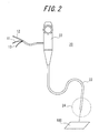
- FIG. 2 is a schematic overview of the scope 20.
- the scope 20 includes an operation part 22 and an insertion part 23.
- the optical fiber 11 for illumination, the optical fiber bundle 12 for detection, and a wiring cable 13 extending from the control device body 30 are each connected to the operation part 22.
- the optical fiber 11 for illumination, optical fiber bundle 12 for detection, and wiring cable 13 pass through the insertion part 23 and extend to a tip 24 (the portion within the dotted line in FIG. 2 ) of the insertion part 23.
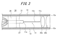
- FIG. 3 is a cross-sectional diagram illustrating an enlargement of the tip 24 of the insertion part 23 of the scope 20 in FIG. 2 .
- the tip 24 of the insertion part 23 of the scope 20 includes the driver 21, projection lenses 25a and 25b (optical system), the optical fiber 11 for illumination that passes through the central portion, and the optical fiber bundle 12 for detection that passes through the peripheral portion.
- the driver 21 drives a tip 11c of the optical fiber 11 for illumination by vibration.
- the driver 21 includes an actuator tube 27 fixed to the inside of the insertion part 23 of the scope 20 by an attachment ring 26, a fiber holding member 29 disposed inside the actuator tube 27, and piezoelectric elements 28a to 28d (see FIGS. 4A and 4B ).
- the optical fiber 11 for illumination is supported by the fiber holding member 29, and the portion from a fixed end 11 a supported by the fiber holding member 29 to the tip 11c is an oscillating part 11b that is supported to allow oscillation.
- the optical fiber bundle 12 for detection is disposed to pass through the peripheral portion of the insertion part 23 and extends to the end of the tip 24.
- a non-illustrated detection lens is also provided at the tip of each fiber in the optical fiber bundle 12 for detection.
- the projection lenses 25a and 25b and the detection lenses are disposed at the extreme end of the tip 24 of the insertion part 23 in the scope 20.
- the projection lenses 25a and 25b are configured so that laser light emitted from the tip 11c of the optical fiber 11 for illumination is irradiated on the object 100 and roughly concentrated.
- the detection lenses are disposed so that light that is reflected, scattered, refracted, or the like by the object 100 (light that interacted with the object 100) due to laser light concentrated on the object 100 is captured, concentrated on the optical fiber bundle 12 for detection disposed behind the detection lenses, and combined.
- the detection lenses are not limited to a double lens structure and may be structured as a single lens or as three or more lenses.
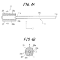
- FIG. 4A illustrates the vibration driving mechanism of the driver 21 of the optical scanning endoscope apparatus 10 and illustrates the oscillating part 11b of the optical fiber 11 for illumination.
- FIG. 4B is a cross-sectional diagram along the A-A line in FIG. 4A .
- the optical fiber 11 for illumination passes through the center of the fiber holding member 29, which has a prismatic shape, and is fixed and held by the fiber holding member 29.
- the four sides of the fiber holding member 29 respectively face the ⁇ Y direction and the ⁇ X direction.
- a pair of piezoelectric elements 28a and 28c for driving in the Y direction are fixed onto the sides of the fiber holding member 29 in the ⁇ Y direction, and a pair of piezoelectric elements 28b and 28d for driving in the X direction are fixed onto the sides in the ⁇ X direction.
- the wiring cable 13 from the drive controller 38 of the control device body 30 is connected to the piezoelectric elements 28a to 28d, which are driven by application of voltage by the drive controller 38.
- the drive controller 38 can perform vibration driving of the piezoelectric elements 28b and 28d for driving in the X direction and the piezoelectric elements 28a and 28c for driving in the Y direction by applying vibration voltage of the same frequency or vibration voltage of different frequencies thereto.
- the oscillating part 11b of the optical fiber 11 for illumination illustrated in FIGS. 3 , 4A, and 4B vibrates, and the tip 11c c is deflected, so that the laser light emitted from the tip 11c sequentially (for example, in a spiral shape) scans the surface of the object 100.
- FIGS. 5A to 5G illustrate an example of the relationship between the light emission timing and the correction timing of the offset value. Time proceeds from the left to the right of the figures.
- the offset correction timing is provided during the scanning period, specifically between predetermined pixels, with R, G, and B light emission constituting one pixel.
- FIGS. 5A to 5C illustrate the light emission timing of the lasers 33R, 33G, and 33B.
- FIG. 5D illustrates the output of the coupler 34.
- FIG. 5E illustrates the output of the photodetector 35.
- FIG. 5F illustrates pixels processed by the signal processor 37.
- FIG. 5G illustrates the timing of correction of the offset value by the offset processor 70.
- the light emission timing controller 32 controls the light emission timing of the lasers 33R, 33G, and 33B in the order of R, G, and B in each light emission cycle T E in accordance with a control signal from the controller 31.
- an electrical signal corresponding to each color output from the photodetector 35 is output to the signal processor 37 via the offset processor 70 and the ADC 36.
- the light emission timing controller 32 Upon reaching the offset correction timing, the light emission timing controller 32 suspends emission of light by all of the lasers 33R, 33G, and 33B for the entire predetermined time T C . During this time, only the electrical signal due to dark current (offset value) is output from the photodetector 35.
- the offset processor 70 corrects the offset value based on the electrical signal output from the photodetector 35.
- the light emission timing controller 32 once again controls the light emission timing of the lasers 33R, 33G, and 33B in the order of R, G, and B in each light emission cycle T E .
- the electrical signal corresponding to each color output from the photodetector 35 is output to the ADC 36 with the offset value having been corrected by the offset processor 70 and is subsequently output to the signal processor 37.
- the signal processor 37 generates image signals based on the R, G, and B electrical signals input sequentially from the photodetector 35 via the offset processor 70 and the ADC 36 and outputs the result to the display 40.
- the pixel that could not be acquired during the predetermined time T C at the offset correction timing is preferably interpolated from neighboring pixels with a known method, thereby preventing the portion corresponding to the predetermined time T C from appearing as a black spot within the image. Good image definition of the image can thus be achieved.
- the "neighboring pixels” referred to here are neighboring pixels along the scanning trajectory of the tip 11c of the optical fiber 11 for illumination or neighboring pixels present upon generation of the image signal output to the display 40.
- FIGS. 6 to 9 Examples of the relationship between the scanning trajectory of the tip 11c of the optical fiber 11 for illumination and the offset correction timing are now described with reference to FIGS. 6 to 9 .
- the solid line t indicates the scanning trajectory of the tip 11c
- the points c represent the position of the tip 11c on the scanning trajectory t at the offset correction timing.
- the first example in FIG. 6 illustrates the case of the tip 11c of the optical fiber 11 for illumination oscillating in a spiral shape from the inner periphery towards the outer periphery due to the driver 21 during the scanning period.
- the offset correction timing is provided during the scanning period each time the tip 11c completes one scanning revolution. Therefore, the positions c of the tip 11c at each offset correction timing are aligned in a row that is vertical in the illustrated example. Accordingly, the portion at each point c at which the offset value is corrected can, for example, be interpolated based on neighboring pixels positioned on either side (to the left and right in the illustrated example) of the row of positions c along the scanning trajectory.
- the black level of the image during the scanning period can be maintained constant, improving image quality.
- the second example in FIG. 7 differs from the first example in that the offset correction timing is provided during the scanning period each time the tip 11c completes 3/4 of a scanning revolution. Therefore, as compared to the first example, the positions c along the scanning trajectory t of the tip 11c at the offset correction timings are farther apart from each other. Accordingly, the pixel at each point c at which the offset value is corrected can, for example, be interpolated based on neighboring pixels that are vertically and horizontally adjacent to the positions c along the scanning trajectory. In this way, according to the second example, the portion at each position c can be interpolated based on a greater number of neighboring pixels than in the first example. Hence, in addition to the effects of the first example, the accuracy of interpolation can be improved, thereby improving the definition of the image.
- the offset correction timing is provided outside the scanning period (outside the display period of the image) when the light source is not emitting light, during the period in which the tip 11c of the optical fiber 11c for illumination returns to the initial position after completion of scanning, for example in a spiral from the outer periphery towards the inner periphery ("return period").
- the offset correction timing may be provided at any timing during the scanning period other than the first and second examples. Also, the first, second, and third examples may for example be combined to provide the offset correction timing both during the scanning period and outside the scanning period.
- the fourth example in FIG. 9 illustrates the case of the tip 11c of the optical fiber 11 for illumination being oscillated in a Lissajous curve by the driver 21 during the scanning period.
- the scanning trajectory of the Lissajous curve passes through the outer peripheral region of the image at least once per revolution.
- "through the outer peripheral region of the image” refers to the region at the outer periphery of the image, excluding the central region.
- the offset correction timings are provided while the tip 11c of the optical fiber 11 for illumination passes through the outer peripheral region of the image (in greater detail, at the upper edge of the image).
- the black level of the image during the scanning period can be maintained constant by providing the offset correction timing during the scanning period, thereby improving image quality. Furthermore, since there is no portion in the central region of the image for which light emission of the light source is suspended, sufficiently good image quality can be obtained even without interpolating the pixels that cannot be acquired at the offset correction timings. Furthermore, by using the scanning trajectory in a Lissajous curve, the return period that is required when using a scanning trajectory in a spiral shape is unnecessary, allowing continuous scanning to be maintained. Hence, the offset value can be corrected frequently, which is particularly advantageous when the variation in the offset value is intense.
- Any trajectory other than the trajectory in a spiral shape and a Lissajous curve described in the first to fourth examples may also be used in this disclosure.
- Embodiment 1 even when the offset value of the electrical signal output from the photodetector 35 varies due to the usage environment, such as the temperature, the black level of the image is maintained constant by correcting the offset value. The image quality can thus be improved.
- FIG. 10 is a block diagram schematically illustrating the structure of an optical scanning endoscope apparatus that is an example of an optical scanning observation apparatus according to Embodiment 2.
- This embodiment only differs from Embodiment 1 in that the control device body 30 further includes an offset processing determiner 72. Therefore, a description of the remaining structure is omitted.
- the offset value is corrected when light emission of the light source is suspended. Even if light emission of the light source is suspended, however, a detected value of external light also ends up being output in addition to the offset value due to dark current from the photodetector 35 when the tip 24 of the insertion part 23 of the scope 20 is outside of a dark field, such as being outside of a patient's body. In this case, the offset value cannot be accurately corrected. To address this issue, the offset value is not corrected in this embodiment when the tip 24 of the insertion part 23 of the scope 20 is outside of a dark field, thereby avoiding inaccurate correction of the offset value.
- the offset processing determiner 72 is connected to the photodetector 35, the offset processor 70, and the light emission timing controller 32. Based on the electrical signal output from the photodetector 35 when the light emission timing controller 32 has suspended light emission of the light source, the offset processing determiner 72 determines whether correction of the offset value is feasible and notifies the offset processor 70 of the determination result. When the offset processing determiner 72 determines that correction of the offset value is feasible, the offset processor 70 corrects the offset value as described in Embodiment 1.
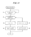
- FIG. 11 is a flowchart illustrating processing by the offset processing determiner 72.
- the offset processing determiner 72 determines whether the light emission timing controller 32 has suspended light emission of the light source (step S1).
- the time during which light emission of the light source is suspended is the predetermined time T C at the offset correction timing during the scanning period or is a time outside the scanning period.
- the offset processing determiner 72 determines whether the value of the electrical signal output from the photodetector 35 is less than a predetermined threshold (step S2).
- This threshold is preferably set to the minimum output value that is envisioned as being output from the photodetector 35 when the tip 24 of the insertion part 23 of the scope 20 is outside of a dark field (such as being outside of a patient's body). The threshold may be changed, however, in accordance with the environment in which the optical scanning endoscope apparatus 10 is used.
- step S2 When the value of the electrical signal output from the photodetector 35 is less than the threshold (step S2: Yes), the offset processing determiner 72 determines that the tip 24 of the insertion part 23 of the scope 20 is in a dark field (step S3), determines that correction of the offset value is feasible (step S4), and notifies the offset processor 70 of the determination result. After receiving this notification, the offset processor 70 corrects the offset value as described in Embodiment 1 at the offset correction timing.
- step S2 determines that the tip 24 of the insertion part 23 of the scope 20 is outside of a dark field (step S5), determines that correction of the offset value is not feasible (step S6), and notifies the offset processor 70 of the determination result. After receiving this notification, the offset processor 70 does not correct the offset value even when reaching the offset correction timing. In this case, the electrical signal output from the photodetector 35 is output to the ADC 36 with the offset value in an uncorrected state.
- the offset value is not corrected when the tip 24 of the insertion part 23 of the scope 20 is outside of a dark field, thereby avoiding inaccurate correction of the offset value.
- the offset processing determiner 72 may proceed to step S2 when determining that the current time is within the predetermined time T C at the offset correction timing based on notification from the light emission timing controller 32.
- the offset processing determiner 72 may proceed to step S3 when determining that the waveform of the electrical signal output from the photodetector 35 during the light emission period of the light source immediately before light emission of the light source is suspended has a pulse shape, i.e. when determining that an object is being scanned.
- the waveform has a pulse shape refers to the output waveform from the photodetector 35 not being an approximately flat shape but rather having a peak each time the colors of R, G, and B are detected, as illustrated in FIG. 5E .
- means for sampling the output signal from the photodetector 35 over an immediately previous predetermined time at predetermined time intervals needs to be provided separately. Based on data of the output signal sampled by this means, the offset processing determiner 72 determines whether the output waveform of the photodetector 35 has a pulse shape.
- the structure of the offset processor 70 is not limited to correcting the offset value in an analog signal state and may instead correct the offset value after conversion to a digital signal.
- the offset processor 70 may correct the offset value by converting to analog the offset value that has been converted from analog to digital by the ADC 36 and then performing feedback control so that the converted offset value becomes a constant value.
- the offset processor 70 may be connected to the output side of the ADC 36 and may correct the offset value that has been converted from analog to digital by the ADC 36 so that the offset value matches the black level of the image.
- the drive controller 38 may be provided internally with a different clock generator than the clock generator 71 used by the controller 31 and may be configured to operate based on a clock signal from this internal clock generator. In this case, as compared to when the controller 31 and the drive controller 38 share use of the clock generator 71, the power consumption can be reduced by the amount of power that would have been required for distributing the clock signal to the drive controller 38.
- the light source of the optical scanning endoscope apparatus 10 is not limited to being configured with the lasers 33R, 33G, and 33B.
- a white light source that emits pulsed light may be provided.
- the driver 21 of the optical fiber 11 for illumination is not limited to use of piezoelectric elements.
- a permanent magnet fixed to the optical fiber 11 for illumination and coils for generation of a deflecting magnetic field (magnet coils) that drive the permanent magnet may be used instead.
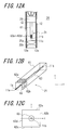
- FIGS. 12A to 12C The following describes a modification to the driver 21 with reference to FIGS. 12A to 12C.
- FIG. 12A is a cross-sectional diagram of the tip 24 of the scope 20
- FIG. 12B is an enlarged perspective view of the driver 21 in FIG. 12A
- FIG. 12A is a cross-sectional diagram of the tip 24 of the scope 20
- FIG. 12B is an enlarged perspective view of the driver 21 in FIG. 12A
- FIG. 12C is a cross-sectional view along a plane perpendicular to the axis of the optical fiber 11 for illumination, illustrating a portion including the coils 62a to 62d for generation of a deflecting magnetic field and the permanent magnet 63 in FIG. 12B .
- the permanent magnet 63 which is magnetized in the axial direction of the optical fiber 11 for illumination and includes a through-hole, is joined to the optical fiber 11 for illumination by the optical fiber 11 being passed through the through-hole.
- a square tube 61 one end of which is fixed to the attachment ring 26, is provided so as to surround the oscillating part 11b, and flat coils 62a to 62d for generation of a deflecting magnetic field are provided on the sides of the square tube 61 at a portion thereof opposing one pole of the permanent magnet 63.
- the pair of coils 62a and 62c for generation of a deflecting magnetic field in the Y direction and the pair of coils 62b and 62d for generation of a deflecting magnetic field in the X direction are each disposed on opposing sides of the square tube 61, and a line connecting the center of the coil 62a for generation of a deflecting magnetic field with the center of the coil 62c for generation of a deflecting magnetic field is orthogonal to a line connecting the center of the coil 62b for generation of a deflecting magnetic field with the center of the coil 62d for generation of a deflecting magnetic field near the central axis of the square tube 61 when the optical fiber 11 for illumination is disposed therein at rest.
- These coils are connected to the drive controller 38 of the control device body 30 via the wiring cable 13 and are driven by drive current from the drive controller 38.
- optical scanning observation apparatus of this disclosure can be applied not only to an optical scanning endoscope apparatus, but also to another optical scanning observation apparatus such as an optical scanning microscope.
Landscapes
- Health & Medical Sciences (AREA)
- Life Sciences & Earth Sciences (AREA)
- Physics & Mathematics (AREA)
- Surgery (AREA)
- Optics & Photonics (AREA)
- Engineering & Computer Science (AREA)
- Biomedical Technology (AREA)
- Veterinary Medicine (AREA)
- Biophysics (AREA)
- Pathology (AREA)
- Radiology & Medical Imaging (AREA)
- Nuclear Medicine, Radiotherapy & Molecular Imaging (AREA)
- Public Health (AREA)
- Heart & Thoracic Surgery (AREA)
- Medical Informatics (AREA)
- Molecular Biology (AREA)
- Animal Behavior & Ethology (AREA)
- General Health & Medical Sciences (AREA)
- General Physics & Mathematics (AREA)
- Signal Processing (AREA)
- Astronomy & Astrophysics (AREA)
- Multimedia (AREA)
- Instruments For Viewing The Inside Of Hollow Bodies (AREA)
- Endoscopes (AREA)
- Mechanical Optical Scanning Systems (AREA)
Abstract
Description
- The present application claims priority to Japanese Patent Application No.
2014-11413 filed on January 24, 2014 - This disclosure relates to an optical scanning observation apparatus that optically scans an object by vibrating an optical fiber.
- A known medical probe for observing an object using pulsed light of various wavelengths that is irradiated from a light source includes optical guiding means for guiding pulsed light incident from the light source and for emitting the pulsed light onto the object and optical delay means for providing a predetermined delay time that differs for each wavelength to reflected pulsed light of the object that is irradiated by the emitted pulsed light, the medical probe outputting the pulsed light provided with the delay time to predetermined photodetector means (for example, see
JP 2010-42128 A - PTL 1:
JP 2010-42128 A - In general, the offset value, due to dark current (black level), of the electrical signal output from the photodetector means may vary (normally, drift) depending on the usage environment, such as the temperature. If the offset value varies, image quality may worsen. The technique disclosed in
PTL 1, however, takes no measures to control worsening of image quality due to such variation in the offset value. - Therefore, focusing on this point, it would be helpful to provide an optical scanning observation apparatus that can improve image quality.
- An optical scanning observation apparatus according to this disclosure is for scanning an object with light from a light source and acquiring an image of the object, the optical scanning observation apparatus including:
- a light emission timing controller configured to control a light emission timing of the light source;
- a fiber configured to guide light from the light source and emit the light toward the object from a tip of the fiber, the tip being supported to allow oscillation;
- a driver configured to drive the tip of the fiber by vibration;
- a photodetector configured to detect light obtained from the object and convert the light obtained from the object to an electrical signal;
- an offset processor configured to correct an offset value based on the electrical signal output by the photodetector while the light emission timing controller suspends light emission of the light source; and
- a signal processor configured to generate an image signal based on the electrical signal for which the offset value was corrected by the offset processor.
- The driver may oscillate the tip of the fiber in a spiral shape.
- The driver may oscillate the tip of the fiber in a Lissajous curve.
- The light emission timing controller may suspend light emission of the light source, and the offset processor may correct the offset value, in an outer peripheral region of an image generated based on the image signal or outside a display period of the image.
- The optical scanning observation apparatus may further include an offset processing determiner configured to determine whether correction of the offset value is feasible based on the electrical signal output by the photodetector while the light emission timing controller suspends light emission of the light source; and
the offset processor may correct the offset value when the offset processing determiner determines that correction of the offset value is feasible. - We thus provide an optical scanning observation apparatus that can improve image quality.
- In the accompanying drawings:
-
FIG. 1 is a block diagram schematically illustrating the structure of an optical scanning endoscope apparatus that is an example of an optical scanning observation apparatus according toEmbodiment 1; -
FIG. 2 is a schematic overview of the scope inFIG. 1 ; -
FIG. 3 is a cross-sectional diagram of the tip of the scope inFIG. 2 ; -
FIG. 4A is a side view, andFIG. 4B is a cross-sectional diagram along the A-A line inFIG. 4A , illustrating the driver and the oscillating portion of the optical fiber for illumination inFIG. 3 ; -
FIGS. 5A to 5G illustrate an example of the relationship between the light emission timing and the correction timing of the offset value; -
FIG. 6 illustrates a first example of the relationship between the scanning trajectory and the correction timing of the offset value; -
FIG. 7 illustrates a second example of the relationship between the scanning trajectory and the correction timing of the offset value; -
FIG. 8 illustrates a third example of the relationship between the scanning trajectory and the correction timing of the offset value; -
FIG. 9 illustrates a fourth example of the relationship between the scanning trajectory and the correction timing of the offset value; -
FIG. 10 is a block diagram schematically illustrating the structure of an optical scanning endoscope apparatus that is an example of an optical scanning observation apparatus according toEmbodiment 2; -
FIG. 11 is a flowchart illustrating processing by the offset processing determiner inFIG. 10 ; and -
FIGS. 12A to 12C illustrate modifications to the driver inFIG. 4 , whereFIG. 12A is a cross-sectional diagram of the tip of the scope,FIG. 12B is an enlarged perspective view of the driver inFIG. 12A, and FIG. 12C is a cross-sectional view along a plane perpendicular to the axis of the optical fiber, illustrating a portion including the coils for generation of a deflecting magnetic field and the permanent magnet inFIG. 12B . - Embodiments are described below with reference to the drawings.
- With reference to
FIGS. 1 to 9 ,Embodiment 1 is described.FIG. 1 is a block diagram schematically illustrating the structure of an optical scanning endoscope apparatus that is an example of an optical scanning observation apparatus according toEmbodiment 1. InFIG. 1 , an opticalscanning endoscope apparatus 10 includes ascope 20, acontrol device body 30, and adisplay 40. - First, the structure of the
control device body 30 is described. Thecontrol device body 30 includes acontroller 31 that controls the opticalscanning endoscope apparatus 10 overall, aclock generator 71, a lightemission timing controller 32,lasers coupler 34, adrive controller 38, aphotodetector 35, anoffset processor 70, an analog/digital converter (ADC) 36, and asignal processor 37. - The timing for correcting (also referred to below as "offset correction") the offset value due to dark current (black level) of the electrical signal output from the
photodetector 35 is stored in advance in a memory (not illustrated) that is readable and writable by thecontroller 31. As described below in detail, the offset correction timing may be provided during the scanning period (i.e. within the display period of the image) or outside the scanning period (i.e. outside the display period of the image). - In accordance with a control signal from the
controller 31, the lightemission timing controller 32 controls the light emission timing of thelasers - The
lasers emission timing controller 32 being emitted at a timing selected by the lightemission timing controller 32. For example, Diode-Pumped Solid-State (DPSS) lasers or laser diodes may be used as thelasers - In this disclosure, the "light emission cycle TE" does not refer to the light emission cycle of each of the
lasers - The laser light emitted from the
lasers coupler 34 and is incident as illumination light on anoptical fiber 11 for illumination (fiber) that is a single-mode fiber. Thecoupler 34 may, for example, be configured using a dichroic prism or the like. - The
lasers coupler 34 may be stored in a housing that is separate from thecontrol device body 30 and is joined to thecontrol device body 30 by a signal wire. - Light incident on the
optical fiber 11 for illumination from thecoupler 34 is guided to the tip of thescope 20 and irradiated towards anobject 100. At this time, by driving thedriver 21 of thescope 20 by vibration, thedrive controller 38 of thecontrol device body 30 drives the tip of theoptical fiber 11 for illumination by vibration. As a result, the illumination light emitted from theoptical fiber 11 for illumination scans the observation surface of theobject 100 in 2D, for example in a spiral shape. Light such as reflected light or scattered light that is obtained from theobject 100 due to irradiation with the illumination light is received at the tip of anoptical fiber bundle 12 for detection, which is constituted by multi-mode fibers, and is guided through thescope 20 to thecontrol device body 30. - In this embodiment, the "scanning period" refers to the period over which illumination light emitted from the
optical fiber 11 for illumination is used for 2D scanning of the observation surface of theobject 100. - In each light emission cycle TE of the light source, the
photodetector 35 detects light obtained via theoptical fiber bundle 12 for detection from theobject 100 due to irradiation by light of one of the colors R, G, and B and outputs an analog signal (electrical signal) limited to the bandwidth of the color. - When the light
emission timing controller 32 suspends light emission of the light source, the offsetprocessor 70 corrects the offset value (black level) based on an electrical signal output from thephotodetector 35 due to dark current. In greater detail, upon being notified by the lightemission timing controller 32 that the offset correction timing has been reached, the offsetprocessor 70 corrects the offset value. The time during which light emission is suspended at the offset correction timing (also referred to below as the "predetermined time at the offset correction timing") TC is set in advance to be at least the length of time necessary to correct the offset value. The offsetprocessor 70 corrects the offset value for example by clamping the electrical signal from thephotodetector 35 and setting the black level of the electrical signal to a predetermined voltage. Once an electrical signal is output from thephotodetector 35 after the offset correction timing, the offsetprocessor 70 outputs the electrical signal with the corrected offset value to theADC 36. - The
ADC 36 converts the analog signal with the corrected offset value, which was input from thephotodetector 35 via the offsetprocessor 70, to a digital signal (electrical signal) and outputs the result to thesignal processor 37. - The
signal processor 37 associates the digital signals having corrected offset values, which were input from theADC 36 at each light emission cycle TE, with the respective light emission timings and scanning positions, and stores the results sequentially in memory (not illustrated). Information on the light emission timing and scanning position is acquired from thecontroller 31. Thecontroller 31 calculates information on the scanning position along the scanning path from information such as the amplitude and phase of vibration voltage applied by thedrive controller 38. After completion of scanning or during the scanning period, thesignal processor 37 generates an image signal by performing necessary image processing, such as enhancement, y processing, and interpolation, based on each digital signal input from theADC 36 and displays an image of theobject 100 on thedisplay 40. - The
clock generator 71 is connected to thecontroller 31 and the lightemission timing controller 32 and outputs a reference clock signal to thecontroller 31 and the lightemission timing controller 32. Thecontroller 31 divides the clock signal from theclock generator 71 to generate the control timing of thedriver 21 by thedrive controller 38 and the sampling timing by theADC 36. On the other hand, the lightemission timing controller 32 divides the clock signal from theclock generator 71 to generate the light emission timing of thelasers processor 70. In this way, by causing the lightemission timing controller 32,drive controller 38, andADC 36 to operate based on the clock signal from thesame clock generator 71, these operations can be reliably synchronized to allow reliable correction of the offset value without any misalignment in the timing. - Next, the structure of the
scope 20 is described.FIG. 2 is a schematic overview of thescope 20. Thescope 20 includes anoperation part 22 and aninsertion part 23. Theoptical fiber 11 for illumination, theoptical fiber bundle 12 for detection, and awiring cable 13 extending from thecontrol device body 30 are each connected to theoperation part 22. Theoptical fiber 11 for illumination,optical fiber bundle 12 for detection, andwiring cable 13 pass through theinsertion part 23 and extend to a tip 24 (the portion within the dotted line inFIG. 2 ) of theinsertion part 23. -
FIG. 3 is a cross-sectional diagram illustrating an enlargement of thetip 24 of theinsertion part 23 of thescope 20 inFIG. 2 . Thetip 24 of theinsertion part 23 of thescope 20 includes thedriver 21,projection lenses optical fiber 11 for illumination that passes through the central portion, and theoptical fiber bundle 12 for detection that passes through the peripheral portion. - The
driver 21 drives atip 11c of theoptical fiber 11 for illumination by vibration. Thedriver 21 includes anactuator tube 27 fixed to the inside of theinsertion part 23 of thescope 20 by anattachment ring 26, afiber holding member 29 disposed inside theactuator tube 27, andpiezoelectric elements 28a to 28d (seeFIGS. 4A and 4B ). Theoptical fiber 11 for illumination is supported by thefiber holding member 29, and the portion from afixed end 11 a supported by thefiber holding member 29 to thetip 11c is anoscillating part 11b that is supported to allow oscillation. Theoptical fiber bundle 12 for detection is disposed to pass through the peripheral portion of theinsertion part 23 and extends to the end of thetip 24. A non-illustrated detection lens is also provided at the tip of each fiber in theoptical fiber bundle 12 for detection. - Furthermore, the
projection lenses tip 24 of theinsertion part 23 in thescope 20. Theprojection lenses tip 11c of theoptical fiber 11 for illumination is irradiated on theobject 100 and roughly concentrated. The detection lenses are disposed so that light that is reflected, scattered, refracted, or the like by the object 100 (light that interacted with the object 100) due to laser light concentrated on theobject 100 is captured, concentrated on theoptical fiber bundle 12 for detection disposed behind the detection lenses, and combined. The detection lenses are not limited to a double lens structure and may be structured as a single lens or as three or more lenses. -
FIG. 4A illustrates the vibration driving mechanism of thedriver 21 of the opticalscanning endoscope apparatus 10 and illustrates theoscillating part 11b of theoptical fiber 11 for illumination.FIG. 4B is a cross-sectional diagram along the A-A line inFIG. 4A . Theoptical fiber 11 for illumination passes through the center of thefiber holding member 29, which has a prismatic shape, and is fixed and held by thefiber holding member 29. The four sides of thefiber holding member 29 respectively face the ±Y direction and the ±X direction. A pair ofpiezoelectric elements fiber holding member 29 in the ±Y direction, and a pair ofpiezoelectric elements - The
wiring cable 13 from thedrive controller 38 of thecontrol device body 30 is connected to thepiezoelectric elements 28a to 28d, which are driven by application of voltage by thedrive controller 38. - Voltage of equivalent magnitude and opposite sign is always applied across the
piezoelectric elements piezoelectric elements piezoelectric elements fiber holding member 29 therebetween expands and the other contracts, thereby causing thefiber holding member 29 to flex. Repeating this operation produces vibration in the X direction. The same is true for vibration in the Y direction as well. - The
drive controller 38 can perform vibration driving of thepiezoelectric elements piezoelectric elements piezoelectric elements piezoelectric elements oscillating part 11b of theoptical fiber 11 for illumination illustrated inFIGS. 3 ,4A, and 4B vibrates, and thetip 11c c is deflected, so that the laser light emitted from thetip 11c sequentially (for example, in a spiral shape) scans the surface of theobject 100. - Next, the operation of the optical
scanning endoscope apparatus 10 is described with reference toFIGS. 5A to 5G , focusing on processing by the lightemission timing controller 32, offsetprocessor 70, andsignal processor 37.FIGS. 5A to 5G illustrate an example of the relationship between the light emission timing and the correction timing of the offset value. Time proceeds from the left to the right of the figures. In the example inFIGS. 5A to 5G , the offset correction timing is provided during the scanning period, specifically between predetermined pixels, with R, G, and B light emission constituting one pixel.FIGS. 5A to 5C illustrate the light emission timing of thelasers FIG. 5D illustrates the output of thecoupler 34.FIG. 5E illustrates the output of thephotodetector 35.FIG. 5F illustrates pixels processed by thesignal processor 37.FIG. 5G illustrates the timing of correction of the offset value by the offsetprocessor 70. - During the scanning period excluding the offset correction timing, the light
emission timing controller 32 controls the light emission timing of thelasers controller 31. During this time, an electrical signal corresponding to each color output from thephotodetector 35 is output to thesignal processor 37 via the offsetprocessor 70 and theADC 36. - Upon reaching the offset correction timing, the light
emission timing controller 32 suspends emission of light by all of thelasers photodetector 35. The offsetprocessor 70 corrects the offset value based on the electrical signal output from thephotodetector 35. - At the end of the offset correction timing that lasts throughout the predetermined time TC, the light
emission timing controller 32 once again controls the light emission timing of thelasers photodetector 35 is output to theADC 36 with the offset value having been corrected by the offsetprocessor 70 and is subsequently output to thesignal processor 37. - As illustrated in
FIG. 5F , thesignal processor 37 generates image signals based on the R, G, and B electrical signals input sequentially from thephotodetector 35 via the offsetprocessor 70 and theADC 36 and outputs the result to thedisplay 40. At this time, the pixel that could not be acquired during the predetermined time TC at the offset correction timing is preferably interpolated from neighboring pixels with a known method, thereby preventing the portion corresponding to the predetermined time TC from appearing as a black spot within the image. Good image definition of the image can thus be achieved. The "neighboring pixels" referred to here are neighboring pixels along the scanning trajectory of thetip 11c of theoptical fiber 11 for illumination or neighboring pixels present upon generation of the image signal output to thedisplay 40. - Examples of the relationship between the scanning trajectory of the
tip 11c of theoptical fiber 11 for illumination and the offset correction timing are now described with reference toFIGS. 6 to 9 . In the figures, the solid line t indicates the scanning trajectory of thetip 11c, whereas the points c represent the position of thetip 11c on the scanning trajectory t at the offset correction timing. - The first example in
FIG. 6 illustrates the case of thetip 11c of theoptical fiber 11 for illumination oscillating in a spiral shape from the inner periphery towards the outer periphery due to thedriver 21 during the scanning period. In this example, the offset correction timing is provided during the scanning period each time thetip 11c completes one scanning revolution. Therefore, the positions c of thetip 11c at each offset correction timing are aligned in a row that is vertical in the illustrated example. Accordingly, the portion at each point c at which the offset value is corrected can, for example, be interpolated based on neighboring pixels positioned on either side (to the left and right in the illustrated example) of the row of positions c along the scanning trajectory. By providing the offset correction timing during the scanning period, the black level of the image during the scanning period can be maintained constant, improving image quality. - The second example in
FIG. 7 differs from the first example in that the offset correction timing is provided during the scanning period each time thetip 11c completes 3/4 of a scanning revolution. Therefore, as compared to the first example, the positions c along the scanning trajectory t of thetip 11c at the offset correction timings are farther apart from each other. Accordingly, the pixel at each point c at which the offset value is corrected can, for example, be interpolated based on neighboring pixels that are vertically and horizontally adjacent to the positions c along the scanning trajectory. In this way, according to the second example, the portion at each position c can be interpolated based on a greater number of neighboring pixels than in the first example. Hence, in addition to the effects of the first example, the accuracy of interpolation can be improved, thereby improving the definition of the image. - In the third example illustrated in
FIG. 8 , the offset correction timing is provided outside the scanning period (outside the display period of the image) when the light source is not emitting light, during the period in which thetip 11c of theoptical fiber 11c for illumination returns to the initial position after completion of scanning, for example in a spiral from the outer periphery towards the inner periphery ("return period"). By providing the offset correction timing during the return period, the quality of the image displayed during the next scan can be improved. Furthermore, since there is no portion in the image for which light emission of the light source is suspended, it is not necessary to perform the interpolation processing that, in the case of providing the offset correction timing during the scanning period, is required for the pixel that cannot be acquired at the offset correction timing. - The offset correction timing may be provided at any timing during the scanning period other than the first and second examples. Also, the first, second, and third examples may for example be combined to provide the offset correction timing both during the scanning period and outside the scanning period.
- The fourth example in
FIG. 9 illustrates the case of thetip 11c of theoptical fiber 11 for illumination being oscillated in a Lissajous curve by thedriver 21 during the scanning period. The scanning trajectory of the Lissajous curve passes through the outer peripheral region of the image at least once per revolution. Here, "through the outer peripheral region of the image" refers to the region at the outer periphery of the image, excluding the central region. In this example, the offset correction timings are provided while thetip 11c of theoptical fiber 11 for illumination passes through the outer peripheral region of the image (in greater detail, at the upper edge of the image). According to this example, as in the first and second examples, the black level of the image during the scanning period can be maintained constant by providing the offset correction timing during the scanning period, thereby improving image quality. Furthermore, since there is no portion in the central region of the image for which light emission of the light source is suspended, sufficiently good image quality can be obtained even without interpolating the pixels that cannot be acquired at the offset correction timings. Furthermore, by using the scanning trajectory in a Lissajous curve, the return period that is required when using a scanning trajectory in a spiral shape is unnecessary, allowing continuous scanning to be maintained. Hence, the offset value can be corrected frequently, which is particularly advantageous when the variation in the offset value is intense. - Any trajectory other than the trajectory in a spiral shape and a Lissajous curve described in the first to fourth examples may also be used in this disclosure.
- According to
Embodiment 1, even when the offset value of the electrical signal output from thephotodetector 35 varies due to the usage environment, such as the temperature, the black level of the image is maintained constant by correcting the offset value. The image quality can thus be improved. - With reference to
FIGS. 10 to 11 ,Embodiment 2 is described.FIG. 10 is a block diagram schematically illustrating the structure of an optical scanning endoscope apparatus that is an example of an optical scanning observation apparatus according toEmbodiment 2. This embodiment only differs fromEmbodiment 1 in that thecontrol device body 30 further includes an offsetprocessing determiner 72. Therefore, a description of the remaining structure is omitted. - In
Embodiment 1, the offset value is corrected when light emission of the light source is suspended. Even if light emission of the light source is suspended, however, a detected value of external light also ends up being output in addition to the offset value due to dark current from thephotodetector 35 when thetip 24 of theinsertion part 23 of thescope 20 is outside of a dark field, such as being outside of a patient's body. In this case, the offset value cannot be accurately corrected. To address this issue, the offset value is not corrected in this embodiment when thetip 24 of theinsertion part 23 of thescope 20 is outside of a dark field, thereby avoiding inaccurate correction of the offset value. - As illustrated in
FIG. 10 , the offsetprocessing determiner 72 is connected to thephotodetector 35, the offsetprocessor 70, and the lightemission timing controller 32. Based on the electrical signal output from thephotodetector 35 when the lightemission timing controller 32 has suspended light emission of the light source, the offsetprocessing determiner 72 determines whether correction of the offset value is feasible and notifies the offsetprocessor 70 of the determination result. When the offsetprocessing determiner 72 determines that correction of the offset value is feasible, the offsetprocessor 70 corrects the offset value as described inEmbodiment 1. - Next, the operation of the optical
scanning endoscope apparatus 10 is described with reference toFIG. 11 , focusing on processing by the offsetprocessing determiner 72.FIG. 11 is a flowchart illustrating processing by the offsetprocessing determiner 72. First, based on notification from the lightemission timing controller 32, the offsetprocessing determiner 72 determines whether the lightemission timing controller 32 has suspended light emission of the light source (step S1). Here, the time during which light emission of the light source is suspended is the predetermined time TC at the offset correction timing during the scanning period or is a time outside the scanning period. - Upon determining that the light
emission timing controller 32 has suspended light emission of the light source (step S1: Yes), the offsetprocessing determiner 72 determines whether the value of the electrical signal output from thephotodetector 35 is less than a predetermined threshold (step S2). This threshold is preferably set to the minimum output value that is envisioned as being output from thephotodetector 35 when thetip 24 of theinsertion part 23 of thescope 20 is outside of a dark field (such as being outside of a patient's body). The threshold may be changed, however, in accordance with the environment in which the opticalscanning endoscope apparatus 10 is used. - When the value of the electrical signal output from the
photodetector 35 is less than the threshold (step S2: Yes), the offsetprocessing determiner 72 determines that thetip 24 of theinsertion part 23 of thescope 20 is in a dark field (step S3), determines that correction of the offset value is feasible (step S4), and notifies the offsetprocessor 70 of the determination result. After receiving this notification, the offsetprocessor 70 corrects the offset value as described inEmbodiment 1 at the offset correction timing. - Conversely, when the value of the electrical signal output from the
photodetector 35 is equal to or greater than the threshold in step S2 (step S2: No), the offsetprocessing determiner 72 determines that thetip 24 of theinsertion part 23 of thescope 20 is outside of a dark field (step S5), determines that correction of the offset value is not feasible (step S6), and notifies the offsetprocessor 70 of the determination result. After receiving this notification, the offsetprocessor 70 does not correct the offset value even when reaching the offset correction timing. In this case, the electrical signal output from thephotodetector 35 is output to theADC 36 with the offset value in an uncorrected state. - According to
Embodiment 2, in addition to the effects ofEmbodiment 1, the offset value is not corrected when thetip 24 of theinsertion part 23 of thescope 20 is outside of a dark field, thereby avoiding inaccurate correction of the offset value. - Instead of step S1 in
FIG. 11 , the offsetprocessing determiner 72 may proceed to step S2 when determining that the current time is within the predetermined time TC at the offset correction timing based on notification from the lightemission timing controller 32. - Instead of step S2 in
FIG. 11 , or in addition to step S2, the offsetprocessing determiner 72 may proceed to step S3 when determining that the waveform of the electrical signal output from thephotodetector 35 during the light emission period of the light source immediately before light emission of the light source is suspended has a pulse shape, i.e. when determining that an object is being scanned. Stating that "the waveform has a pulse shape" refers to the output waveform from thephotodetector 35 not being an approximately flat shape but rather having a peak each time the colors of R, G, and B are detected, as illustrated inFIG. 5E . In this case, means for sampling the output signal from thephotodetector 35 over an immediately previous predetermined time at predetermined time intervals needs to be provided separately. Based on data of the output signal sampled by this means, the offsetprocessing determiner 72 determines whether the output waveform of thephotodetector 35 has a pulse shape. - In
Embodiments processor 70 is not limited to correcting the offset value in an analog signal state and may instead correct the offset value after conversion to a digital signal. For example, the offsetprocessor 70 may correct the offset value by converting to analog the offset value that has been converted from analog to digital by theADC 36 and then performing feedback control so that the converted offset value becomes a constant value. Alternatively, the offsetprocessor 70 may be connected to the output side of theADC 36 and may correct the offset value that has been converted from analog to digital by theADC 36 so that the offset value matches the black level of the image. - In
Embodiments drive controller 38 may be provided internally with a different clock generator than theclock generator 71 used by thecontroller 31 and may be configured to operate based on a clock signal from this internal clock generator. In this case, as compared to when thecontroller 31 and thedrive controller 38 share use of theclock generator 71, the power consumption can be reduced by the amount of power that would have been required for distributing the clock signal to thedrive controller 38. - In
Embodiments scanning endoscope apparatus 10 is not limited to being configured with thelasers - Furthermore, in
Embodiments driver 21 of theoptical fiber 11 for illumination is not limited to use of piezoelectric elements. For example, a permanent magnet fixed to theoptical fiber 11 for illumination and coils for generation of a deflecting magnetic field (magnet coils) that drive the permanent magnet may be used instead. The following describes a modification to thedriver 21 with reference toFIGS. 12A to 12C. FIG. 12A is a cross-sectional diagram of thetip 24 of thescope 20,FIG. 12B is an enlarged perspective view of thedriver 21 inFIG. 12A, and FIG. 12C is a cross-sectional view along a plane perpendicular to the axis of theoptical fiber 11 for illumination, illustrating a portion including thecoils 62a to 62d for generation of a deflecting magnetic field and thepermanent magnet 63 inFIG. 12B . - At a portion of the
oscillating part 11b of theoptical fiber 11 for illumination, thepermanent magnet 63, which is magnetized in the axial direction of theoptical fiber 11 for illumination and includes a through-hole, is joined to theoptical fiber 11 for illumination by theoptical fiber 11 being passed through the through-hole. Asquare tube 61, one end of which is fixed to theattachment ring 26, is provided so as to surround theoscillating part 11b, andflat coils 62a to 62d for generation of a deflecting magnetic field are provided on the sides of thesquare tube 61 at a portion thereof opposing one pole of thepermanent magnet 63. - The pair of
coils coils square tube 61, and a line connecting the center of thecoil 62a for generation of a deflecting magnetic field with the center of thecoil 62c for generation of a deflecting magnetic field is orthogonal to a line connecting the center of thecoil 62b for generation of a deflecting magnetic field with the center of thecoil 62d for generation of a deflecting magnetic field near the central axis of thesquare tube 61 when theoptical fiber 11 for illumination is disposed therein at rest. These coils are connected to thedrive controller 38 of thecontrol device body 30 via thewiring cable 13 and are driven by drive current from thedrive controller 38. - The optical scanning observation apparatus of this disclosure can be applied not only to an optical scanning endoscope apparatus, but also to another optical scanning observation apparatus such as an optical scanning microscope.
Claims (5)
- An optical scanning observation apparatus for scanning an object with light from a light source and acquiring an image of the object, the optical scanning observation apparatus comprising:a light emission timing controller configured to control a light emission timing of the light source;a fiber configured to guide light from the light source and emit the light toward the object from a tip of the fiber, the tip being supported to allow oscillation;a driver configured to drive the tip of the fiber by vibration;a photodetector configured to detect light obtained from the object and convert the light obtained from the object to an electrical signal;an offset processor configured to correct an offset value based on the electrical signal output by the photodetector while the light emission timing controller suspends light emission of the light source; anda signal processor configured to generate an image signal based on the electrical signal for which the offset value was corrected by the offset processor.
- The optical scanning observation apparatus of claim 1, wherein the driver oscillates the tip of the fiber in a spiral shape.
- The optical scanning observation apparatus of claim 1, wherein the driver oscillates the tip of the fiber in a Lissajous curve.
- The optical scanning observation apparatus of any one of claims 1 to 3, wherein the light emission timing controller suspends light emission of the light source, and the offset processor corrects the offset value, in an outer peripheral region of an image generated based on the image signal or outside a display period of the image.
- The optical scanning observation apparatus of any one of claims 1 to 3, further comprising:an offset processing determiner configured to determine whether correction of the offset value is feasible based on the electrical signal output by the photodetector while the light emission timing controller suspends light emission of the light source;wherein the offset processor corrects the offset value when the offset processing determiner determines that correction of the offset value is feasible.
Applications Claiming Priority (2)
| Application Number | Priority Date | Filing Date | Title |
|---|---|---|---|
| JP2014011413A JP6397191B2 (en) | 2014-01-24 | 2014-01-24 | Optical scanning observation device |
| PCT/JP2015/000302 WO2015111412A1 (en) | 2014-01-24 | 2015-01-23 | Optical scanning-type observing device |
Publications (2)
| Publication Number | Publication Date |
|---|---|
| EP3097844A1 true EP3097844A1 (en) | 2016-11-30 |
| EP3097844A4 EP3097844A4 (en) | 2017-12-20 |
Family
ID=53681222
Family Applications (1)
| Application Number | Title | Priority Date | Filing Date |
|---|---|---|---|
| EP15740622.4A Withdrawn EP3097844A4 (en) | 2014-01-24 | 2015-01-23 | Optical scanning-type observing device |
Country Status (5)
| Country | Link |
|---|---|
| US (1) | US10151916B2 (en) |
| EP (1) | EP3097844A4 (en) |
| JP (1) | JP6397191B2 (en) |
| CN (1) | CN105916431B (en) |
| WO (1) | WO2015111412A1 (en) |
Families Citing this family (6)
| Publication number | Priority date | Publication date | Assignee | Title |
|---|---|---|---|---|
| WO2016116968A1 (en) * | 2015-01-23 | 2016-07-28 | オリンパス株式会社 | Optical scanning device |
| JP6553183B2 (en) * | 2015-06-23 | 2019-07-31 | オリンパス株式会社 | Driving condition setting device for optical scanning device |
| DE112016006140T5 (en) * | 2016-02-29 | 2018-09-13 | Olympus Corporation | Imaging / projection device with optical scanning and endoscope system |
| WO2017203585A1 (en) * | 2016-05-23 | 2017-11-30 | オリンパス株式会社 | Correction value acquisition device, image processing device, optical scanning observation system, correction value acquisition method, and image processing method |
| JP7784429B2 (en) * | 2021-06-29 | 2025-12-11 | 浜松ホトニクス株式会社 | Optical image processing method, machine learning method, trained model, machine learning preprocessing method, optical image processing module, optical image processing program, and optical image processing system |
| CN115412689B (en) * | 2022-07-26 | 2023-04-25 | 瀚湄信息科技(上海)有限公司 | Dark field noise processing method and device based on dynamic calibration and electronic equipment |
Family Cites Families (14)
| Publication number | Priority date | Publication date | Assignee | Title |
|---|---|---|---|---|
| JP2002360510A (en) * | 2001-06-08 | 2002-12-17 | Fuji Photo Film Co Ltd | Endoscopic apparatus and control method for the same |
| US7448995B2 (en) * | 2003-06-23 | 2008-11-11 | Microvision, Inc. | Scanning endoscope |
| JP3813961B2 (en) * | 2004-02-04 | 2006-08-23 | オリンパス株式会社 | Endoscope signal processing device |
| JP4667754B2 (en) * | 2004-02-23 | 2011-04-13 | オリンパス株式会社 | Light receiving device for scanning laser microscope and scanning laser microscope using the same |
| US7436564B2 (en) * | 2005-08-03 | 2008-10-14 | Seiko Epson Corporation | Light scanning apparatus and method to prevent damage to an oscillation mirror in an abnormal control condition via a detection signal outputted to a controller even though the source still emits light |
| US7813586B2 (en) * | 2006-08-07 | 2010-10-12 | Mela Sciences, Inc. | Reducing noise in digital images |
| JP2009136459A (en) * | 2007-12-05 | 2009-06-25 | Hoya Corp | Noise reduction system, endoscope processor, and endoscope system |
| JP2010042128A (en) | 2008-08-12 | 2010-02-25 | Hoya Corp | Medical probe and medical observation system |
| JP5388732B2 (en) * | 2009-07-15 | 2014-01-15 | Hoya株式会社 | Medical observation system and processor |
| JP2012085715A (en) * | 2010-10-18 | 2012-05-10 | Fujifilm Corp | Endoscopic device |
| JP5282173B2 (en) * | 2011-03-31 | 2013-09-04 | オリンパスメディカルシステムズ株式会社 | Scanning endoscope device |
| JP2013178417A (en) * | 2012-02-29 | 2013-09-09 | Hoya Corp | Calibration device |
| JP2013244045A (en) * | 2012-05-23 | 2013-12-09 | Olympus Corp | Scanning endoscope apparatus |
| JP6067309B2 (en) * | 2012-10-02 | 2017-01-25 | Hoya株式会社 | Endoscope system and endoscope processor |
-
2014
- 2014-01-24 JP JP2014011413A patent/JP6397191B2/en active Active
-
2015
- 2015-01-23 CN CN201580005031.9A patent/CN105916431B/en active Active
- 2015-01-23 WO PCT/JP2015/000302 patent/WO2015111412A1/en not_active Ceased
- 2015-01-23 EP EP15740622.4A patent/EP3097844A4/en not_active Withdrawn
-
2016
- 2016-07-21 US US15/215,626 patent/US10151916B2/en active Active
Also Published As
| Publication number | Publication date |
|---|---|
| US20160327782A1 (en) | 2016-11-10 |
| JP2015136573A (en) | 2015-07-30 |
| JP6397191B2 (en) | 2018-09-26 |
| EP3097844A4 (en) | 2017-12-20 |
| CN105916431B (en) | 2018-01-12 |
| CN105916431A (en) | 2016-08-31 |
| US10151916B2 (en) | 2018-12-11 |
| WO2015111412A1 (en) | 2015-07-30 |
Similar Documents
| Publication | Publication Date | Title |
|---|---|---|
| US10151916B2 (en) | Optical scanning observation apparatus | |
| US10151914B2 (en) | Optical scanning observation apparatus | |
| US10025087B2 (en) | Optical scanning observation apparatus | |
| CN104081250A (en) | Optical Scanning Observation Device | |
| US20160150948A1 (en) | Optical scanning unit, optical scanning observation apparatus, and optical fiber scanning apparatus | |
| US20170311779A1 (en) | Optical scanning endoscope apparatus | |
| US20170099421A1 (en) | Optical scanning endoscope apparatus | |
| EP3150101A1 (en) | Optical scan observation device and optical scan observation device operation method | |
| US20170227755A1 (en) | Optical scanning endoscope apparatus | |
| US10754143B2 (en) | Optical scanning method and optical scanning apparatus | |
| US20170318181A1 (en) | Optical scanning method and optical scanning apparatus | |
| US20170090185A1 (en) | Optical scanning apparatus and optical scanning observation apparatus | |
| US9977236B2 (en) | Optical scanning method and optical scanning apparatus | |
| JP6180335B2 (en) | Optical scanning endoscope device | |
| US10491873B2 (en) | Scanning observation apparatus and image display method of scanning observation apparatus | |
| US20180309915A1 (en) | Optical scanning observation apparatus and method for adjusting irradiation parameter of pulsed laser light | |
| JP6424035B2 (en) | Optical scanning observation apparatus and pulsed laser beam irradiation parameter adjustment method | |
| WO2017109814A1 (en) | Light scanning observation device | |
| JPWO2017195256A1 (en) | Optical scanning observation apparatus and optical scanning observation method |
Legal Events
| Date | Code | Title | Description |
|---|---|---|---|
| PUAI | Public reference made under article 153(3) epc to a published international application that has entered the european phase |
Free format text: ORIGINAL CODE: 0009012 |
|
| 17P | Request for examination filed |
Effective date: 20160725 |
|
| AK | Designated contracting states |
Kind code of ref document: A1 Designated state(s): AL AT BE BG CH CY CZ DE DK EE ES FI FR GB GR HR HU IE IS IT LI LT LU LV MC MK MT NL NO PL PT RO RS SE SI SK SM TR |
|
| AX | Request for extension of the european patent |
Extension state: BA ME |
|
| DAX | Request for extension of the european patent (deleted) | ||
| A4 | Supplementary search report drawn up and despatched |
Effective date: 20171117 |
|
| RIC1 | Information provided on ipc code assigned before grant |
Ipc: A61B 1/04 20060101AFI20171113BHEP Ipc: A61B 1/00 20060101ALI20171113BHEP |
|
| STAA | Information on the status of an ep patent application or granted ep patent |
Free format text: STATUS: REQUEST FOR EXAMINATION WAS MADE |
|
| STAA | Information on the status of an ep patent application or granted ep patent |
Free format text: STATUS: THE APPLICATION IS DEEMED TO BE WITHDRAWN |
|
| 18D | Application deemed to be withdrawn |
Effective date: 20200801 |