EP3096199A1 - Clock signal alignment for system-in-package (sip) devices - Google Patents
Clock signal alignment for system-in-package (sip) devices Download PDFInfo
- Publication number
- EP3096199A1 EP3096199A1 EP16169245.4A EP16169245A EP3096199A1 EP 3096199 A1 EP3096199 A1 EP 3096199A1 EP 16169245 A EP16169245 A EP 16169245A EP 3096199 A1 EP3096199 A1 EP 3096199A1
- Authority
- EP
- European Patent Office
- Prior art keywords
- delay
- semiconductor device
- clock signal
- clock
- die
- Prior art date
- Legal status (The legal status is an assumption and is not a legal conclusion. Google has not performed a legal analysis and makes no representation as to the accuracy of the status listed.)
- Granted
Links
Images



Classifications
-
- G—PHYSICS
- G06—COMPUTING OR CALCULATING; COUNTING
- G06F—ELECTRIC DIGITAL DATA PROCESSING
- G06F1/00—Details not covered by groups G06F3/00 - G06F13/00 and G06F21/00
- G06F1/04—Generating or distributing clock signals or signals derived directly therefrom
- G06F1/12—Synchronisation of different clock signals provided by a plurality of clock generators
-
- G—PHYSICS
- G06—COMPUTING OR CALCULATING; COUNTING
- G06F—ELECTRIC DIGITAL DATA PROCESSING
- G06F1/00—Details not covered by groups G06F3/00 - G06F13/00 and G06F21/00
- G06F1/04—Generating or distributing clock signals or signals derived directly therefrom
- G06F1/10—Distribution of clock signals, e.g. skew
-
- G—PHYSICS
- G06—COMPUTING OR CALCULATING; COUNTING
- G06F—ELECTRIC DIGITAL DATA PROCESSING
- G06F13/00—Interconnection of, or transfer of information or other signals between, memories, input/output devices or central processing units
- G06F13/14—Handling requests for interconnection or transfer
- G06F13/16—Handling requests for interconnection or transfer for access to memory bus
- G06F13/1668—Details of memory controller
- G06F13/1689—Synchronisation and timing concerns
-
- G—PHYSICS
- G06—COMPUTING OR CALCULATING; COUNTING
- G06F—ELECTRIC DIGITAL DATA PROCESSING
- G06F13/00—Interconnection of, or transfer of information or other signals between, memories, input/output devices or central processing units
- G06F13/38—Information transfer, e.g. on bus
- G06F13/40—Bus structure
- G06F13/4063—Device-to-bus coupling
- G06F13/4068—Electrical coupling
- G06F13/4072—Drivers or receivers
-
- G—PHYSICS
- G06—COMPUTING OR CALCULATING; COUNTING
- G06F—ELECTRIC DIGITAL DATA PROCESSING
- G06F30/00—Computer-aided design [CAD]
- G06F30/30—Circuit design
- G06F30/32—Circuit design at the digital level
- G06F30/33—Design verification, e.g. functional simulation or model checking
- G06F30/3308—Design verification, e.g. functional simulation or model checking using simulation
- G06F30/3312—Timing analysis
-
- G—PHYSICS
- G06—COMPUTING OR CALCULATING; COUNTING
- G06F—ELECTRIC DIGITAL DATA PROCESSING
- G06F30/00—Computer-aided design [CAD]
- G06F30/30—Circuit design
- G06F30/39—Circuit design at the physical level
- G06F30/394—Routing
-
- G—PHYSICS
- G06—COMPUTING OR CALCULATING; COUNTING
- G06F—ELECTRIC DIGITAL DATA PROCESSING
- G06F30/00—Computer-aided design [CAD]
- G06F30/30—Circuit design
- G06F30/39—Circuit design at the physical level
- G06F30/396—Clock trees
-
- H—ELECTRICITY
- H03—ELECTRONIC CIRCUITRY
- H03K—PULSE TECHNIQUE
- H03K19/00—Logic circuits, i.e. having at least two inputs acting on one output; Inverting circuits
- H03K19/02—Logic circuits, i.e. having at least two inputs acting on one output; Inverting circuits using specified components
- H03K19/173—Logic circuits, i.e. having at least two inputs acting on one output; Inverting circuits using specified components using elementary logic circuits as components
- H03K19/177—Logic circuits, i.e. having at least two inputs acting on one output; Inverting circuits using specified components using elementary logic circuits as components arranged in matrix form
- H03K19/17736—Structural details of routing resources
-
- H—ELECTRICITY
- H03—ELECTRONIC CIRCUITRY
- H03K—PULSE TECHNIQUE
- H03K5/00—Manipulating of pulses not covered by one of the other main groups of this subclass
- H03K5/13—Arrangements having a single output and transforming input signals into pulses delivered at desired time intervals
- H03K5/135—Arrangements having a single output and transforming input signals into pulses delivered at desired time intervals by the use of time reference signals, e.g. clock signals
-
- G—PHYSICS
- G06—COMPUTING OR CALCULATING; COUNTING
- G06F—ELECTRIC DIGITAL DATA PROCESSING
- G06F2119/00—Details relating to the type or aim of the analysis or the optimisation
- G06F2119/12—Timing analysis or timing optimisation
Definitions
- This disclosure relates generally to system-in-package (SiP) devices, and more specifically, to clock signal alignment across integrated circuits within SiP devices.
- SiP technology currently attempts to interconnect numerous semiconductor devices within a single semiconductor package.
- SiP technology includes various interconnect techniques, such as utilizing copper pillar interconnects, flip-chip interconnects, interconnect fabric such as interposers, and the like.
- An integrated circuit often includes synchronous elements, or elements that must be synchronized using a clock signal.
- the clock signal may arrive at the elements at different times due to various factors affecting the clock signal, such as differing path length to the elements, temperature variation, electromagnetic interference, resistive-capacitive coupling, propagation delays of buffers used in the clock distribution network, and the like.
- clock skew must be reduced by balancing the clock signal across the integrated circuit to ensure that the synchronous elements receive logic level changes of the clock signal simultaneously.
- SiP System-in-package
- SiP devices semiconductor devices
- the integrated circuits of the different SiP devices also include synchronous elements.
- Many high performance applications require synchronous communication within an SiP package, where the various synchronous elements of the SiP devices must be synchronized.
- Present solutions often utilize clock domain crossing logic within interfacing logic on each interconnected interface of the SiP devices.
- clock domain crossing can cause significant latency penalties for high performance applications as signals cross from one clock domain to another clock domain and must be synchronized to the destination clock domain.
- the present disclosure provides adaptive clock signal alignment across synchronous elements of multiple SiP devices within an SiP package that implements a single clock domain by compensating for interconnect delay.
- a source clock signal is provided by a master or host device to one or more secondary or expansion devices of an SiP package.
- the source clock signal experiences delay when traveling across SiP interconnect circuitry from the host device to a given expansion device, also referred to as interconnect delay.
- the interconnect delay is compensated for by each expansion device to properly align local clock signal(s) with the host device's source clock signal.
- Each expansion device includes local synchronous logic that utilizes the local aligned clock signal(s), achieving synchronous communication with the host device's synchronous logic that utilizes the source clock signal.
- the interconnect delay is determined for each expansion device and set before operation of the SiP package (e.g., during factory settings). In other embodiments, the interconnect delay is dynamically (e.g., on the fly) determined by each expansion device during operation of the SiP package. In both types of embodiments, adaptive clock signal alignment compensates for the interconnect delay and automatically adjusts a local clock signal to be aligned with the source clock signal of the host device. In this manner, the present disclosure provides a flexible and low latency solution for partitioning synchronous elements within the same clock domain onto multiple SiP devices, where the SiP devices achieve synchronous communication at high speeds (e.g., greater than or equal to 1 GHz), even for differing SiP technologies.
- high speeds e.g., greater than or equal to 1 GHz
- FIG. 1 illustrates a simplified block diagram depicting an example semiconductor device 105 of a system 100 in which the disclosure is implemented.
- semiconductor device 105 is a die 105 that is part of an expansion device included in a system-in-package (SiP) package, which also includes a host die (not shown).
- SiP system-in-package
- semiconductor device 105 and a host semiconductor device are part of a single die, where the semiconductor device 105 and the source semiconductor device are intraconnected devices on the single die. It is noted that semiconductor device 105 is described herein as die 105 for illustrative purposes, and should not be taken to be limiting. While die 105 includes a great variety of components, many components are omitted in FIG. 1 to maintain simplicity.
- Die 105 includes on-chip synchronous logic 125, or integrated circuitry that includes synchronous elements.
- On-chip synchronous logic 125 is configured to be in synchronous communication with synchronous logic on a host die (not shown) via a number of data lines 195, level shifter 110, and a number of data lines 197. Also, bus and address control lines (not shown) are associated with data lines 195 and 197.
- An example embodiment of on-chip synchronous logic 125 includes a synchronous bus that is configured to be in synchronous communication with a synchronous bus on the host die, which is further discussed below in connection with FIG. 2 .
- Die 105 also includes interconnect circuitry configured to provide an interface to communicate with another die, such as a host die.
- Interconnect circuitry may be any one of various interconnect technologies, such as copper pillar interconnect technology (e.g., for stacked devices), flip-chip interconnect technology (e.g., for flip-chip devices), interconnect fabric (e.g., for some types of SiP devices), and the like.
- Some embodiments of interconnect technology also include technology translation circuitry, such as level shift circuitry that allows die of different technologies to communicate with one another.
- the embodiment illustrated in FIG. 1 shows die 105 having interconnect circuitry including technology translation circuitry, which is illustrated as level shifter 110.
- Level shifter 110 is configured to adjust signals received from a host die (not shown) to a level utilized by internal circuitry of die 105, as well as to adjust outgoing signals to a level utilized by the host die for transmission to the host die. In some embodiments, level shifter 110 translates signals between some standard signal level at the interconnect and an internal signal level utilized by internal circuitry of die 105 when receiving or transmitting such signals. As such, die 105 is agnostic as to the type of die with which die 105 communicates.
- Die 105 is configured to receive a source clock signal 160 from a host die.
- Source clock 160 is input to level shifter 110, which outputs a level shifted version of the source clock 160, also referred to herein as a received source clock signal 170.
- level shifter 110 As source clock 160 travels from the host die to die 105 via interconnect circuitry, source clock 160 experiences delay arising from the interconnect circuitry, also referred to herein as interconnect delay 165.
- interconnect delay 165 For example, source clock 160 experiences delay 115 from level shifter 110 due to a variety of reasons, including but not limited to propagation delay of logic or buffer circuitry within level shifter 110, signal path length, temperature variation, electromagnetic interference, resistive-capacitive coupling, and the like.
- interconnect delay 165 is an amount of delay that is introduced to source clock signal 160 as it travels from a point where source clock 160 is available to synchronous elements on the host die (e.g., is used to clock synchronous logic on host die) through interconnect circuitry (including through level shifter 110) to a point where received source clock signal 170 is available to clock aligning block 120.
- interconnect delay 165 is modeled to include level shifter (LS) delay 115.
- Die 105 also includes a clock alignment loop circuit, which in turn includes a clock aligning block 120, a clock control block 130, a clock distribution network 140, and a clock delay circuit 150.
- the clock alignment loop circuit includes a generated clock signal path from clock aligning block 120 to clock distribution network 140 (via clock control block 130), and a feedback clock signal path from clock distribution network 140 to clock aligning block 120 (via clock delay circuit 150).
- the clock alignment loop circuit is configured to align one or more local clock signals, or aligned clock(s) 185 as discussed below, with source clock signal 160 to achieve a single clock domain.
- Clock aligning block 120 has two inputs, the received source clock signal 170 and a feedback clock signal received from clock delay circuit 150, which is illustrated as intermediate adjusted clock 190.
- the feedback clock signal is further discussed below in connection with clock delay circuit 150.
- Clock aligning block 120 is configured to compare phases of the received source clock signal 170 and the feedback clock signal to determine a delay (or phase difference) exhibited by the feedback clock signal, as compared with the received source clock signal 170.
- Clock aligning block 120 is also configured to output a master adjusted clock signal 175 whose phase is adjusted in order to compensate for the delay exhibited by the feedback clock signal. Such delay is further discussed below in connection with clock delay circuit 150.
- Examples of circuitry included in clock aligning block 120 include, but are not limited to, a phase detector, a variable delay line, a variable frequency oscillator, a delay- locked loop (DLL) circuit (e.g., a phase detector coupled with a variable delay line), a phase-locked loop (PLL) circuit (e.g., a phase detector coupled with a variable frequency oscillator), and similar circuitry that is configured to output an adjustable periodic clock signal.
- DLL delay- locked loop
- PLL phase-locked loop
- Clock control block 130 is configured to receive master adjusted clock signal 175 and to output one or more generated clock signals 180.
- One or more generated clock signals 180 may each have a different clock frequency, where each clock signal 180 has a frequency that is some factor (e.g., multiple or fraction) of the frequency of master adjusted clock signal 175.
- Examples of circuitry included in clock control block 130 include, but are not limited to, clock frequency divider circuits, clock frequency multiplier circuits, and similar circuitry that is configured to receive an input clock signal and generate one or more clock signals based on the frequency of the input clock signal.
- Clock distribution network 140 is configured to distribute the one or more generated clock signals 180 as one or more balanced clock signals 185 to synchronous elements of logic circuitry on die 105, including to on-chip synchronous logic 125.
- Clock distribution network 140 is balanced, where the clock signals are distributed to the synchronous elements in such a way that the synchronous elements receive logic level changes of the clock signals simultaneously.
- clock distribution network 140 provides one or more balanced clock signals 185 to on-chip synchronous logic 125.
- One or more balanced clock signals 185 may be phase aligned with one another.
- One or more balanced clock signals 185 may each have a different clock frequency, where each clock signal 185 has a frequency that is some factor (e.g., multiple or fraction) of the frequency of master adjusted clock signal 175.
- Examples of circuitry included in clock distribution network 140 include, but is not limited to, balanced clock trees, buffers to drive synchronous elements (e.g., registers) at the leaves of the clock tree, de-skew circuits, de-jitter circuits, and the like.
- clock control block 130 includes data latches, such as D-type flip flops that include various logic gate elements, where each data latch requires a certain amount of time after a clock edge is received for its output to change, also referred to as clock-to-output propagation delay.
- the overall propagation delay introduced into generated clocks 180 (as compared with master adjusted clock 175) by clock control block 130 is referred to as CCB (clock control block) delay 135.
- the buffers in clock distribution network 140 which also include various logic gate elements, also each require a certain amount of time to change its output after a clock edge is received.
- the overall propagation delay introduced into balanced clocks 185 is referred to as CDN (clock distribution network) delay 145.
- CDN delay 145 often change during operation of die 105 for a variety of reasons, including but not limited to voltage supply variation, temperature variation, electromagnetic interference, resistive-capacitive coupling, and the like.
- Clock delay circuit 150 is configured to receive one of the balanced clock signals 185 (also referred to as a feedback balanced clock signal 185) and to output a delayed version of the feedback balanced clock signal 185 as intermediate adjusted clock signal 190, which is provided to clock aligning block 120 as the feedback clock signal.
- Clock delay circuit 150 includes a delay element configured to introduce some delay into the feedback balanced clock signal 185 according to delay value 155, which results in intermediate adjusted clock signal 190.
- Delay value 155 corresponds to the interconnect delay 165 from host die to die 105.
- delay value 155 is a delay control signal (e.g., a voltage signal that is proportional to interconnect delay 165) utilized by clock delay circuit 150 to control the delay element (e.g., a variable delay line or a variable frequency oscillator) to introduce a delay time into feedback balanced clock signal 185, where the delay time is equal to interconnect delay 165.
- delay value 155 is one or more delay control signals utilized to control one or more delay elements.
- delay value 155 is a delay code or other numerical value that represents the delay time equal to interconnect delay 165.
- Clock delay circuit 150 is configured to determine a delay control signal corresponding to delay value 155, where the delay control signal is utilized to control the delay element to introduce the delay time (equal to interconnect delay 165) into feedback balanced clock signal 185.
- delay value 155 is determined at some time before operation of die 105 (e.g., during factory setting), where interconnect delay 165 is measured and a delay value 155 corresponding to the measured interconnect delay 165 is programmed in clock delay circuit 150 (e.g., in a register or other data storage element). In other embodiments, delay value 155 is provided by a user at a time during operation of die 105.
- Examples of circuitry included in clock delay circuit 150 include, but are not limited to, a variable delay line, a variable frequency oscillator, and the like.
- clock aligning block 120 compares received source clock signal 170 and intermediate adjusted clock signal 190, clock aligning block 120 is configured to output a master adjusted clock signal 175 that is adjusted to compensate for delay exhibited by intermediate adjusted clock signal 190. It is noted that received source clock signal 170 is a delayed version of source clock signal 160 due to interconnect delay 165 and intermediate adjusted clock signal 190 is a delayed version of the feedback balanced clock signal 185 with a delay time equal to interconnect delay 165.
- phase aligning block 120 also adjusts master adjusted clock signal 175 to compensate for other delay exhibited by intermediate adjusted clock signal 190, including CCB delay 135 and CDN delay 145.
- the aligned clock signals 185 are used to clock on-chip synchronous logic 125 on die 105, while source clock signal 160 is used to clock synchronous logic on the host die.
- One or more aligned clock signals 185 may each have a different clock frequency, where each clock signal 185 has a frequency that is some factor (e.g., multiple or fraction) of the frequency of master adjusted clock signal 175 or intermediate adjusted clock signal 190.
- an aligned clock signal 185 provided to on-chip synchronous logic 125 may have a clock frequency divided by two or four, as compared with the clock frequency of intermediate adjusted clock signal 190.
- a similarly divided clock signal may also be provided to synchronous logic on the host die. This results in synchronous communication between on-chip synchronous logic 125 on die 105 and synchronous logic on the host die. In this manner, a solution for aligning clock signals utilizing a static delay value is provided in FIG. 1 .
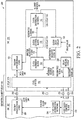
- FIG. 2 illustrates a simplified block diagram depicting an example semiconductor device 205 of a system 200 in which the disclosure is implemented.
- semiconductor device 205 is a die 205 that is an expansion device included in a system-in-package (SiP) package 200, which also includes host die 207.
- semiconductor device 205 and a host semiconductor device 207 are part of a single die, where the semiconductor device 205 and host semiconductor device 207 are intraconnected devices on the single die. While die 205 and 207 include a great variety of components, many components are omitted in FIG. 2 to maintain simplicity.
- Die 205 includes a number of components discussed above in connection with FIG. 1 , where like reference numbers indicate similar components.
- die 205 includes level shifter 110, on-chip synchronous logic 125, clock aligning block 120, clock control block 130, clock distribution network 140, and clock delay circuit 150, which operate as similarly discussed above.
- FIG. 2 includes a level shifter on die 205 and not on die 207, it is noted that other embodiments provide for a level shifter on die 207 and not on die 205. It is also noted that some other embodiments provide for a level shifter on both die 205 and on die 207, and still other embodiments provide that a level shifter is not included on either die 205 or on die 207.
- Die 207 includes a host clock control block 230 that is configured to receive a master adjusted clock signal (not shown) and to output one or more generated clock signals to host clock distribution network 235.
- Host clock distribution network 235 is balanced and distributes one or more clock signals, including source clock signal 160, to on-chip synchronous logic 225 of die 207 in such a way that the synchronous elements receive logic level changes of the distributed clock signals simultaneously.
- On-chip synchronous logic 225 is configured to be in synchronous communication with on-chip synchronous logic 125 via data lines 295, level shifter 110, and data lines 195. Also, bus and address control lines (not shown) are associated with data lines 295 and 195.
- An example embodiment of on-chip synchronous logic 125 and 225 includes a synchronous bus that is configured to provide synchronous communication between die 205 and host die 207.
- Die interconnect delay 165 (or simply interconnect delay 165) is an amount of delay that is introduced to source clock signal 160 as it travels from a point where source clock 160 is available to synchronous elements on host die 207 (e.g., at output of host clock distribution network 235) through interconnect circuitry of host die 207 and interconnect circuitry (including through level shifter 110) of die 205 to a point where received source clock signal 170 is available to clock aligning block 120.
- interconnect delay 165 is modeled to include LS delay 115 and die-to-die delay 250, represented as delay elements 250 in FIG. 2 .
- Die-to-die delay 250 includes delay time introduced by various interconnect circuitry during transmission of source clock signal 160 from host die 207 to die 205 (excluding LS delay 115).
- die-to-die delay 250 may include propagation delay of buffers (not shown) utilized to strengthen source clock signal 160 before and after transmission between die 205 and 207, as well as propagation delay of interconnect circuitry not shown in FIG. 2 .
- die-to-die delay 250 is shown as being a same amount of delay in both directions, from die 205 to host die 207 (e.g., a path shown as node A to node B) and from host die 207 to die 205 (e.g., a path shown as node C to node D).
- die-to-die delay 250 may be a different amount of delay in different directions.
- Die 205 also includes a delay measure circuit 220 that is configured to dynamically measure interconnect delay 165 between host die 207 and die 205 (during operation of die 205) using a loopback path over interconnect circuitry on die 205 that is coupled to interconnect circuitry on host die 207.
- the loopback path is illustrated as a path traveling from delay measure circuit 220 as transmitted signal 240, traverses level shifter 110, traverses remaining interconnect circuitry from die 205 to host die 207 through nodes A and B, traverses the remaining interconnect circuitry returning from host die 207 to die 205 through nodes C and D, traverses level shifter 110, and is received as received signal 245 at delay measure circuit 220.
- node A is located immediately before transmit interconnect circuitry of die 205
- node B is located immediately after receipt interconnect circuitry of host die 207
- node C is located immediately before transmit interconnect circuitry of host die 207
- node D is located immediately after receipt interconnect circuitry of die 205.
- Delay measure circuit 220 is configured to output a transmitted signal 240 (or a measurement signal) through level shifter 110 to host die 207 via the first half of the loopback path.
- Host die 207 receives and returns the signal to die 205 via the second half of the loopback path through level shifter 110, where delay measure circuit 220 receives the returned signal as received signal 245 (or a delayed measurement signal).
- the transmitted signal 240 experiences delay arising from traversing transmit interconnect circuitry on die 205 and receipt interconnect circuitry on host die 207, which is represented as a die-to-die delay element 250 between nodes A and B.
- the transmitted signal 240 also experiences delay arising from traversing transmit interconnect circuitry on host die 207 and receipt interconnect circuitry on die 205, which is also represented as a die-to-die delay element 250 between nodes C and D. Since the loopback path travels to die 207 and back to die 205, the loopback path replicates twice the delay experienced by source clock signal 160 as it travels from die 207 to die 205. As noted above, die-to-die delay 250 is the same amount of delay in both directions in the embodiments discussed herein.
- Delay measure circuit 220 is configured to measure the round-trip delay introduced into the transmitted signal 240 while traveling through level shifter 110 (which is LS delay 115), along the first half of the loopback path through interconnect circuitry of die 205 and 207 (which is die-to-die delay 250), along the second half of the loopback path through interconnect circuitry of die 205 and 207 (which is also die-to-die delay 250), and through level shifter 110 (which is LS delay 115).
- data signals also experience delay from similarly traversing interconnect circuitry on host die 207 and die 205, which is also represented as a die-to-die delay element 250 between nodes N and O, which are on opposing sides of the coupled interconnect circuitry of die 207 and 205 (e.g., node N is similar in position to nodes B and C, while node O is similar in position to nodes A and D).
- Delay measure circuit 220 is configured to measure the round-trip delay by comparing phases of the transmitted signal 240 (measurement signal) and the received signal 245 (delayed measurement signal) to determine the phase difference between the transmitted signal 240 and the received signal 245. The phase difference indicates the total round-trip delay.
- Delay measure circuit 220 is configured to divide the total round-trip delay by two to determine the (one-way) interconnect delay 165 between host die 207 and die 205. Delay measure circuit 220 then outputs a delay value 255 to clock delay circuit 150, where delay value 255 corresponds to the interconnect delay 165.
- delay value 255 is a delay control signal (e.g., a voltage signal that is proportional to interconnect delay 165) utilized by clock delay circuit 150 to control a delay element (e.g., a variable delay line or a variable frequency oscillator) to introduce a delay time into feedback balanced clock signal 185, where the delay time is equal to interconnect delay 165.
- delay value 255 is a delay code or other numerical value that represents the delay time equal to interconnect delay 165.
- Clock delay circuit 150 is configured to determine a delay control signal corresponding to delay value 255, where the delay control signal is utilized to control a delay element that introduces the delay time (equal to interconnect delay 165) into feedback balanced clock signal 185. Since interconnect delay 165 is determined dynamically, delay value 255 is provided dynamically to clock delay circuit 150. Examples of circuitry included in delay measure circuit 220 include, but are not limited to, a phase detector, and the like.
- clock delay circuit 150 is configured to output a delayed version of the feedback balanced clock signal 185, according to delay value 255, as intermediate adjusted clock signal 190, which is provided to clock aligning block 120 as the feedback clock signal.
- clock aligning block 120 compares received source clock signal 170 and intermediate adjusted clock signal 190, clock aligning block 120 is configured to output a master adjusted clock signal 175 that is adjusted to compensate for delay exhibited by intermediate adjusted clock signal 190.
- received source clock signal 170 is a delayed version of source clock signal 160 due to interconnect delay 165 and intermediate adjusted clock signal 190 is a delayed version of the feedback balanced clock signal 185 with a delay time equal to interconnect delay 165.
- phase aligning the delayed versions of source clock signal 160 and balanced clock signal 185 i.e., by phase aligning received source clock signal 170 and intermediate adjusted clock signal 190
- the feedback balanced clock signal 185 (and other balanced clock signals 185 distributed by clock distribution network 140) also become phase aligned with the source clock signal 160.
- Clock aligning block 120 also adjusts master adjusted clock signal 175 to compensate for other delay exhibited by intermediate adjusted clock signal 190, including CCB delay 135 and CDN delay 145.
- the aligned clock signals 185 are used to clock on-chip synchronous logic 125 on die 205, while source clock signal 160 is used to clock synchronous logic 225 on host die 207. This results in synchronous communication between on-chip synchronous logic 125 on die 205 and synchronous logic 225 on host die 207. In this manner, a solution for aligning clock signals utilizing dynamic delay measurement is provided in FIG. 2 .
- FIG. 3 illustrates a simplified block diagram depicting an example semiconductor device 305 of system 300 in which the disclosure is implemented.
- semiconductor device 305 is a die 305 that is included in a system-in-package (SiP) package 300, which also includes host die 307.
- SiP system-in-package
- semiconductor device 305 and a host semiconductor device 307 are part of a single die, where the semiconductor device 305 and the host semiconductor device 307 are intraconnected devices on the single die. While die 305 and 307 include a great variety of components, many components are omitted in FIG. 3 to maintain simplicity.
- Die 305 includes a number of components discussed above in connection with FIG. 1 and 2 , where like reference numbers indicate similar components.
- die 305 includes level shifter 110, on-chip synchronous logic 125, clock control block 130, and clock distribution network 140, which operate as similarly discussed above.
- Host die 307 includes a number of components discussed above in connection with FIG. 2 , where like reference numbers also indicate similar components.
- die 307 includes host clock control block 230, host clock distribution network 235, and on-chip synchronous logic 225, which operate as similarly discussed above.
- Host die 307 and die 305 are configured to be in die-to-die communication via data lines 195, level shifter 110, and data lines 295, as similarly discussed above. While the embodiment illustrated in FIG.
- 3 includes a level shifter on die 305 and not on die 307, it is noted that other embodiments provide for a level shifter on die 307 and not on die 305. It is also noted that some other embodiments provide for a level shifter on both die 305 and on die 307, and still other embodiments provide that a level shifter is not included on either die 305 or on die 307.
- Die 305 includes a clock alignment loop circuit, which in turn includes an interconnect delay clock adjusting block 310, a combined delay clock adjusting block 320, an on-chip delay measure circuit 330, an on-chip delay clock adjusting block 340, a clock control block 130, a clock distribution network 140, and an interconnect delay measure circuit 350.
- the clock alignment loop circuit includes a generated clock signal path from interconnect delay clock adjusting block 310 (in combination with interconnect delay measure circuit 350) to clock distribution network 140, and a feedback signal path from clock distribution network 140 to combined delay clock adjusting block 320.
- the clock alignment loop circuit is configured to align one or more local clock signals with source clock signal 160 to achieve a single clock domain between die 307 and die 305.
- Interconnect delay clock adjusting block 310 and interconnect delay measure circuit 350 are configured to dynamically determine interconnect delay 165 using a loopback path during operation of die 305.
- the loopback path is illustrated as a path that traverses through level shifter 110 as received source clock signal 170 is transmitted to die 307, traverses remaining interconnect circuitry from die 305 to die 307 through nodes A and B, traverses the remaining interconnect circuitry returning from host die 307 to die 305 through nodes C and D, traverses level shifter 110, and is received as received signal 245 at interconnect delay measure circuit 350.
- node A is located immediately before transmit interconnect circuitry of die 305
- node B is located immediately after receipt interconnect circuitry of host die 307
- node C is located immediately before transmit interconnect circuitry of host die 307
- node D is located immediately after receipt interconnect circuitry of die 305.
- a transmitted signal or measurement signal
- die-to-die delay element 250 between nodes A and B and between nodes C and D, as similarly discussed above.
- die-to-die delay 250 is the same amount of delay in both directions in the embodiments discussed herein.
- the transmitted signal also experiences delay arising from traversing one or more buffer elements 355 on die 305 and host die 307, where the buffer elements 355 are utilized to strengthen the source clock signal 160 and received source clock signal 170.
- Each buffer 355 also includes logic gate elements and introduces additional propagation delay.
- interconnect delay 165 is modeled to include LS delay 115, die-to-die delay 250 (excluding buffer delay 355 and LS delay 115), and buffer delay 355 on both die 307 and die 305.
- similar buffers 355 may also be implemented to strengthen data lines 295 on die 307 before transmission to die 305 and strengthen data lines 195 after being output by level shifter 110, in some embodiments.
- a buffer delay 360 is implemented on die 307 as part of the loopback path.
- Buffer delay 360 is configured to introduce a delay time equivalent to twice the total buffer delay time introduced by both buffers 355 on die 307 and on die 305.
- buffer delay 360 may represent four buffers 355 connected end to end on die 307 to introduce an equivalent buffer delay in the loopback path in order to accurately represent the total delay experienced by source clock signal 160 traveling round-trip from die 305 to die 307 and back to die 305.
- the loopback path replicates twice the delay experienced by source clock signal 160 as it travels from host die 307 to die 305.
- Interconnect delay measure circuit 350 is configured to measure the total round-trip delay introduced into received source clock signal 170 while traveling along the loopback path.
- the total round-trip delay includes delay through level shifter 110 (which is LS delay 115), along the first half of the loopback path through interconnect circuitry of die 305 and 307 (which is die-to-die delay 250), through buffer delay 360, along the second half of the loopback path through interconnect circuitry of die 305 and 307 (which is also die-to-die delay 250), and through level shifter 110 (which is also LS delay 115).
- Interconnect delay measure circuit 350 has two inputs, the received signal 245 (or the delayed measurement signal) and a delayed clock signal 325 from interconnect delay clock adjusting block 310. Interconnect delay measure circuit 350 is configured to measure the round-trip delay by comparing phases of received signal 245 and the delayed clock signal 325 to determine the phase difference between the received signal 245 and the delayed clock signal 325. The phase difference indicates the round-trip delay. Based on the phase difference, interconnect delay measure circuit 350 is configured to output an increase/decrease (inc/dec) control signal 345, which is provided to interconnect delay clock adjusting block 310.
- inc/dec increase/decrease
- Inc/dec control signal 345 indicates to interconnect delay clock adjusting block 310 whether the phase of the delayed clock signal 325 should be delayed by a greater or lesser amount of delay in order to phase align the delayed clock 325 with the received signal 245. For example, if a positive clock edge of delayed clock signal 325 is received before a positive clock edge of received signal 245, inc/dec control signal 345 indicates that the phase of delayed clock signal 325 should be delayed by a greater amount of delay in order to phase align with received signal 245 (e.g., control signal 345 indicates "increase" to clock adjusting block 310).
- interconnect measure circuit 350 examples include, but are not limited to, a phase detector, and the like.
- Interconnect delay clock adjusting block 310 has two inputs, the received source clock signal 170 and the increase/decrease control signal 345 from interconnect delay measure circuit 350.
- Interconnect delay clock adjusting block 310 is configured to output a delayed version of receive source clock 170 (which is delayed or adjusted according to inc/dec control signal 345, as described above) as the delayed clock signal 325 to interconnect delay measure circuit 350.
- Interconnect delay clock adjusting block 310 also includes tracking circuitry to determine the round-trip delay by accumulating the amount of delay introduced to received source clock signal 170 (which results in delayed clock signal 325) based on the on-going indications of inc/dec control signal 345.
- the phase difference between received source clock 170 and delayed clock signal 325 indicates the round-trip delay, where the phase difference is introduced by interconnect delay measure circuit 350 (e.g., incrementally or otherwise).
- Interconnect delay clock adjusting block 310 is configured to divide the round-trip delay by two to determine the (one-way) interconnect delay 165 from host die 307 to die 305.
- Interconnect delay clock adjusting block 310 then outputs a delay code 315 to combined delay clock adjusting block 320, where delay code 315 represents the delay time equal to interconnect delay 165.
- delay code 315 is also stored at interconnect delay clock adjusting block 310.
- interconnect delay 165 is determined dynamically (and may change due to variations in voltage supply, temperature, electromagnetic interference, and the like)
- delay code 315 is also determined dynamically and provided to combined delay clock adjusting block 320.
- Examples of circuitry included in interconnect delay clock adjusting block 310 include, but are not limited to, a variable delay line, a variable frequency oscillator, and similar circuitry that is configured to output an adjustable periodic clock signal utilized for delay measurement, as well as output a delay code reflecting the delay measurement.
- Combined delay clock adjusting block 320 has two inputs, a feedback balanced clock 185 and the delay code 315.
- Combined delay clock adjusting block 320 includes a delay element and circuitry configured to utilize delay code 315 to set or control the delay element to introduce the delay time (equal to interconnect delay 165) into feedback balanced clock 185, which is output as intermediate adjusted clock 190 to on-chip delay measure circuit 330.
- delay code 315 is a delay control signal (e.g., a voltage signal that is proportional to interconnect delay 165) utilized by combined delay clock adjusting block 320 to control the delay element (e.g., a variable delay line or a variable frequency oscillator) to introduce a delay time (equal to interconnect delay 165) into feedback balanced clock signal 185.
- a delay control signal e.g., a voltage signal that is proportional to interconnect delay 165
- the delay element e.g., a variable delay line or a variable frequency oscillator
- Examples of circuitry included in combined delay clock adjusting block 320 include but are not limited to a variable delay line, a variable frequency oscillator, and similar circuitry that is configured to output an adjustable periodic clock signal.
- On-chip delay measure circuit 330 has two inputs, intermediate adjusted clock 190 and received source clock 170.
- On-chip delay measure circuit 330 is configured to measure on-chip delay by comparing phases of intermediate adjusted clock signal 190 and received source clock signal 170 to determine the phase difference between the phases. The phase difference indicates the on-chip delay, which includes CCB delay 135 and CDN delay 145. Based on the phase difference, on-chip delay measure circuit 330 is configured to output an increase/decrease (inc/dec) control signal 335, which is provided to on-chip delay clock adjusting block 340.
- inc/dec increase/decrease
- Inc/dec control signal 335 indicates to on-chip delay clock adjusting block 340 whether the phase of intermediate adjusted clock 190 should be delayed by a greater or lesser amount of delay in order to phase align intermediate adjusted clock 190 with received source clock signal 170, as similarly discussed above in connection with inc/dec control signal 345 of interconnect delay measure circuit 350.
- Examples of circuitry included in on-chip delay measure circuit 330 include, but are not limited to, a phase detector, and the like.
- On-chip delay clock adjusting block 340 has two inputs, received source clock signal 170 and the increase/decrease control signal 335 from on-chip delay measure circuit 330.
- On-chip delay clock adjusting block 340 is configured to output a delayed version of received source clock 170 (which is delayed or adjusted according to inc/dec control signal 335, as described above) as the master adjusted clock signal 175 to clock control block 130.
- the phase of master adjusted clock signal 175 compensates for on-chip delay (including CCB delay 135 and CDN delay 145) exhibited by intermediate adjusted clock 190, as compared with received source clock 170 by on-chip delay measure circuit 330.
- the phase of master adjusted clock signal 175 also compensates for interconnect delay 165 (including die-to-die delay 250, LS delay 115, and delay arising from one or more buffers 355). Master adjusted clock 175 is provided to clock control block 130, as similarly discussed above.
- received source clock signal 170 is a delayed version of source clock signal 160 due to interconnect delay 165.
- the intermediate adjusted clock signal 190 is a delayed version of the feedback balanced clock signal 185 by a delay time equal to interconnect delay 165.
- the feedback balanced clock signal 185 (and other balanced clock signals 185 distributed by clock distribution network 140) also become phase aligned with the source clock signal 160.
- the aligned clock signals 185 are used to clock on-chip synchronous logic 125 on die 305, while source clock signal 160 is used to clock synchronous logic 225 on the host die 307. This results in synchronous communication between on-chip synchronous logic 125 on die 305 and synchronous logic 225 on the host die 307. In this manner, a solution for aligning clock signals utilizing dynamic delay measurement is provided in FIG. 3 .
- FIG. 4 illustrates waveforms of example clock signals present at a plurality of nodes of a semiconductor device in which the present disclosure is implemented.
- the waveforms illustrate the introduction of delay into source clock signal 160 and the compensation of such delay to achieve aligned clocks 185 that are phase aligned with the source clock signal 160. While the waveforms illustrated in FIG. 4 are explained herein using the embodiment of the present disclosure illustrated in FIG. 2 involving die 205 and host die 207, similar waveforms exist for other embodiments, as will be noted below.
- the illustrated waveforms are present after phase alignment of source clock signal 160 and balanced clock signals 185 (which are also referred to as aligned clock signals 185).
- Source clock signal 160 is illustrated at the top of FIG. 4 , with received clock signal 170 illustrated immediately below. It is noted that a phase difference exists between source clock signal 160 and received clock signal 170, as illustrated by the positive edge of received clock signal 170 following the positive edge of source clock signal 160 by die-to-die delay 250 and level shifter (LS) delay 115. The sum of this delay is interconnect delay 165, and in some embodiments (such as the embodiment discussed in connection with FIG. 1 ) is measured directly at a time prior to device operation (e.g., during a factory setting period of time prior to runtime operation) and a representation of such interconnect delay 165 is programmed as delay value 155 into clock delay circuit 150, as discussed above.
- interconnect delay 165 in some embodiments (such as the embodiment discussed in connection with FIG. 1 ) is measured directly at a time prior to device operation (e.g., during a factory setting period of time prior to runtime operation) and a representation of such interconnect delay 165 is programmed as delay value 155 into clock
- interconnect delay 165 is introduced into aligned clocks 185 prior to clock alignment block 120, which phase aligns received clock signal 170 and intermediate adjusted clock 190. Since both source clock 160 and aligned clocks 185 are delayed by the same amount of interconnect delay 165, source clock signal 160 and aligned clocks 185 are also phase aligned.
- a signal is transmitted on a loopback path that includes nodes A, B, C, and D in order to determine a round trip delay 410, as discussed above.
- transmitted signal 240 is illustrated as the same waveform of received clock signal 170, although transmitted signal 240 may actually be another waveform that has some phase difference from received clock signal 170.
- received clock signal 170 is transmitted to host die 307 and is equivalent to transmitted signal 240 (not labeled in FIG. 3 ), where transmitted signal 240 has the same waveform as received clock signal 170.
- the transmitted signal 240 in the embodiment of FIG. 2 is independent from received clock signal 170, where transmitted signal 240 has a different waveform than received clock signal 170 (and would thus likely have some phase difference from received clock signal 170).
- a phase difference exists between the waveforms of transmitted signal 240 and node A signal, as illustrated by the positive edge of node A signal following the positive edge of transmitted signal 240 by LS delay 115.
- LS delay 115 arises as the transmitted signal 240 traverses LS shifter 110 to node A.
- a phase difference exists between the waveforms of nodes A and B, as illustrated by the positive edge of node B signal following the positive edge of node A signal by die-to-die delay 250.
- Die-to-die delay 250 arises as the node A signal traverses the transmit interconnect circuitry of die 205 and the receipt interconnect circuitry of host die 207 to node B.
- the node C signal is illustrated as the same waveform of node B signal.
- the waveforms of nodes B and C would have a phase difference equal to the buffer delay 360, which would also increase the (overall) interconnect delay 165 and the round-trip delay 410.
- a phase difference exists between the waveforms of nodes C and D, as illustrated by the positive edge of node D following the positive edge of node C by die-to-die delay 250.
- Die-to-die delay 250 arises as the node C signal traverses the transmit interconnect circuitry of host die 207 and the receipt interconnect circuitry of die 205 to node D.
- a phase difference exists between the waveforms of node D and received signal 245, as illustrated by the positive edge of received signal 245 following the positive edge of node D by LS delay 115.
- LS delay 115 arises as the node D signal traverses LS shifter 110 to an input of delay measure circuit 220.
- round-trip delay 410 As the transmitted signal traverses the loopback path, delay introduced to the transmitted signal 240 accumulates, resulting in round trip delay 410. In other words, a phase difference equal to the round-trip delay 410 exists between transmitted signal 240 and received signal 245.
- the round-trip delay 410 is equal to twice the interconnect delay 165. Once the round-trip delay 410 is determined, interconnect delay 165 is determined by dividing round-trip delay 410 by two.
- Master adjusted clock 175 is shown with a phase that has been adjusted to compensate for both on-chip delay and interconnect delay 165.
- clock alignment block 120 is configured to phase align received source clock signal 170 and intermediate adjusted clock 190 by adjusting the delay of master adjusted clock signal 175.
- master adjusted clock 175 experiences CCB delay 135 as it traverses clock control block 130 and is output as one or more generated clock signals 180.
- the generated clock signals 180 then experience CDN delay 145 as the generated clock signals traverse the clock distribution network 140 and are output as aligned clocks 185.
- clock delay circuit 150 introduces delay 165 to aligned clocks 185 immediately before clock alignment block 120, resulting in intermediate adjusted clock 190.
- the position of a rising edge of master adjusted clock 175 is adjusted to compensate for the delays that include CCB delay 135, CDN delay 145, and interconnect delay 165 between master adjusted clock 175 and intermediate adjusted clock 190.
- intermediate adjusted clock 190 is a delayed version of aligned clocks 185 and received clock signal 170 is a delayed version of source clock signal 160
- source clock 160 and aligned clocks 185 are also phase aligned as a result of phase aligning intermediate adjusted clock 190 with received clock signal 170.
- FIG. 5 illustrates waveforms of example data signals present at a plurality of nodes of a semiconductor device in which the disclosure is implemented.
- the waveforms illustrate synchronous communication achieved between two semiconductor devices, or die, within the same clock domain.
- Node O data signal experiences die-to-die delay 250 as the data signal traverses transmit interconnect circuitry of the host die and the receipt interconnect circuitry of the secondary die, as illustrated by the edge of node O valid data following the edge of node N valid data by die-to-die delay 250.
- Node P data signal experiences LS delay 115 as the data signal traverses LS shifter 110 to node P, as illustrated by the edge of node P valid data following the edge of node O valid data by LS delay 115.
- the edge of valid data of node P signal occurs at a time before the next positive edge of aligned clock 185 to satisfy setup time requirements of elements within on-chip synchronous logic 125 of the secondary die.
- the valid data of node P signal also remains stable for a time after the positive edge of aligned clock 185 to satisfy hold time requirements of elements within on-chip synchronous logic 125 of the secondary die.
- Node O data signal experiences LS delay 115 as the data signal traverses LS shifter 110, as illustrated by the edge of node O valid data following the edge of node P valid data by LS delay 115.
- Node N data signal experiences die-to-die delay 250 as the data signal traverses transmit interconnect circuitry of the secondary die and receipt interconnect circuitry of the host die, as illustrated by the edge of node N valid data following the edge of node O valid data by die-to-die delay 250.
- the edge of valid data of node N occurs at a time before the next positive edge of source clock 160 to satisfy setup time requirements of element within on-chip synchronous logic 225 of the host die.
- the valid data of node N signal also remains stable for a time after the positive edge of source clock 160 to satisfy hold time requirements of elements within on-chip synchronous logic 225 of the host die.
- a semiconductor device that includes a clock delay circuit configured to receive a delay value associated with an interconnect delay, where the interconnect delay is measured across interconnect circuitry that communicatively couples a host semiconductor device with the semiconductor device.
- the clock delay circuit is also configured to delay a local clock signal by an amount of delay indicated by the delay value, where the local clock signal is generated on the semiconductor device.
- the semiconductor device also includes a clock alignment block configured to receive a delayed local clock signal from the clock delay circuit, receive a delayed source clock signal, where the delayed source clock signal is received from the host semiconductor device via the interconnect circuitry, and output a master clock signal based on a comparison of the delayed source clock signal and the delayed local clock signal, where the master clock signal is utilized to generate one or more aligned clock signals on the semiconductor device that are aligned with a source clock signal generated on the host semiconductor device.
- a clock alignment block configured to receive a delayed local clock signal from the clock delay circuit, receive a delayed source clock signal, where the delayed source clock signal is received from the host semiconductor device via the interconnect circuitry, and output a master clock signal based on a comparison of the delayed source clock signal and the delayed local clock signal, where the master clock signal is utilized to generate one or more aligned clock signals on the semiconductor device that are aligned with a source clock signal generated on the host semiconductor device.
- the semiconductor device further includes synchronous logic configured to utilize one of the one or more aligned clock signals as a local source clock signal, where the synchronous logic is configured for synchronous communication with host synchronous logic in the host semiconductor device, and the host synchronous logic is configured to utilize the source clock signal.
- the semiconductor device further includes a clock control block configured to utilize the master clock signal to output one or more generated clock signals, where the one or more generated clock signals include a first local delay introduced by the clock control block.
- the semiconductor device further includes a clock distribution network configured to distribute the one or more generated clock signals as one or more aligned clock signals to synchronous elements on the semiconductor device, where the one or more generated clock signals include a second local delay introduced by the clock distribution network, where the clock alignment block is further configured to adjust the master clock signal to compensate for the first local delay and the second local delay.
- a clock distribution network configured to distribute the one or more generated clock signals as one or more aligned clock signals to synchronous elements on the semiconductor device, where the one or more generated clock signals include a second local delay introduced by the clock distribution network
- the clock alignment block is further configured to adjust the master clock signal to compensate for the first local delay and the second local delay.
- the semiconductor device includes a first semiconductor die
- the host semiconductor device includes a second semiconductor die
- the first semiconductor die and the second semiconductor die are included in a package.
- the delay value includes one of a factory-stored nonvolatile value and a user-provided nonvolatile value.
- the semiconductor device further includes a delay measure circuit configured to measure the interconnect delay, where the delay measure circuit is further configured to transmit a measurement signal to the host semiconductor device via the interconnect circuitry, receive a delayed measurement signal from the host semiconductor device via the interconnect circuitry, compare the measurement signal and the delayed measurement signal to determine a round-trip delay, calculate the interconnect delay from the round-trip delay, and output the delay value that indicates the interconnect delay to the clock delay circuit.
- a delay measure circuit configured to measure the interconnect delay
- the delay measure circuit is further configured to transmit a measurement signal to the host semiconductor device via the interconnect circuitry, receive a delayed measurement signal from the host semiconductor device via the interconnect circuitry, compare the measurement signal and the delayed measurement signal to determine a round-trip delay, calculate the interconnect delay from the round-trip delay, and output the delay value that indicates the interconnect delay to the clock delay circuit.
- a further aspect of the above embodiment provides that the delay measure circuit is configured to transmit the measurement signal on a loopback path that includes a first path from an output of the delay measure circuit to the host semiconductor device that traverses the interconnect circuitry and a second path from the host semiconductor device to an input of the delay measure circuit that traverses the interconnect circuitry, and the delay measure circuit is configured to receive the delayed measurement signal from the second path.
- the interconnect circuitry includes a first set of transmit circuitry on the semiconductor device and a first set of receive circuitry on the host semiconductor device
- the interconnect circuitry includes a second set of transmit circuitry on the host semiconductor device and a second set of receive circuitry on the host semiconductor device
- the first path of the loopback path traverses the first sets of transmit and receive circuitry
- the first path is associated with a die-to-die delay
- the second path of the loopback path traverses the second sets of transmit and receive circuitry
- the second path is associated with the die-to-die delay.
- the interconnect circuitry includes a level shifter
- the interconnect delay includes a delay associated with the level shifter
- the first path and the second path of the loopback path each traverse the level shifter.
- the interconnect circuitry includes a first set of buffer elements associated with a first overall buffer delay
- the loopback path traverses a second set of buffer elements associated with a second overall buffer delay
- the second overall buffer delay includes twice the first overall buffer delay
- a method in another embodiment, includes receiving a delay value associated with an interconnect delay, where the interconnect delay is measured across interconnect circuitry that communicatively couples a host semiconductor device with a semiconductor device. The method also includes delaying a local clock signal by an amount of delay indicated by the delay value to produce a delayed local clock signal, where the local clock signal is generated on the semiconductor device; receiving a delayed source clock signal, where the delayed source clock signal is received from the host semiconductor device via the interconnect circuitry; and outputting a master clock signal based on a comparison of the delayed source clock signal and the delayed local clock signal, where the master clock signal is utilized to generate one or more aligned clock signals on the semiconductor device that are aligned with a source clock signal generated on the host semiconductor device.
- the method further includes clocking synchronous logic with one of the one or more aligned clock signals, where the synchronous logic is configured for synchronous communication with host synchronous logic in the host semiconductor device, and the host synchronous logic is configured to utilize the source clock signal.
- the method further includes generating one or more generated clock signals based on the master clock signal, where the one or more generated clock signals include a first local delay introduced by the generating.
- a further aspect of the above embodiment provides that the method further includes distributing the one or more generated clock signals as one or more aligned clock signals to synchronous elements on the semiconductor device, where the one or more aligned clock signals include a second local delay introduced by the distributing; and adjusting the master clock signal to compensate for the first local delay and the second local delay.
- the method further includes measuring the interconnect delay, the measuring includes transmitting a measurement signal to the host semiconductor device via the interconnect circuitry, receiving a delayed measurement signal from the host semiconductor device via the interconnect circuitry, comparing the measurement signal and the delayed measurement signal to determine a round-trip delay, calculating the interconnect delay from the round-trip delay, and outputting the delay value that indicates the interconnect delay to the clock delay circuit.
- a further aspect of the above embodiment provides that the measurement signal is transmitted on a loopback path that includes a first path from the semiconductor device to the host semiconductor device that traverses the interconnect circuitry and a second path from the host semiconductor device to the semiconductor device that traverses the interconnect circuitry, and the delayed measurement signal is received from the second path of the loopback path.
- the interconnect circuitry includes a first set of transmit circuitry on the semiconductor device and a first set of receive circuitry on the host semiconductor device
- the interconnect circuitry includes a second set of transmit circuitry on the host semiconductor device and a second set of receive circuitry on the host semiconductor device
- the first path of the loopback path traverses the first sets of transmit and receive circuitry
- the first path is associated with a die-to-die delay
- the second path of the loopback path traverses the second sets of transmit and receive circuitry
- the second path is associated with the die-to-die delay.
- the interconnect circuitry includes a level shifter
- the interconnect delay includes a delay associated with the level shifter
- the first path and the second path of the loopback path each traverse the level shifter.
- the interconnect circuitry includes a first set of buffer elements associated with a first overall buffer delay
- the loopback path traverses a second set of buffer elements associated with a second overall buffer delay
- the second overall buffer delay includes twice the first overall buffer delay
- a semiconductor device in another embodiment, includes a delay measure circuit configured to determine a round-trip delay based on a comparison of a measurement signal and a delayed measurement signal.
- Interconnect circuitry communicatively couples a host semiconductor device and the semiconductor device, the measurement signal is transmitted to the host semiconductor device via the interconnect circuitry, and the delayed measurement signal is received from the host semiconductor device via the interconnect circuitry.
- the delay measure circuit is also configured to calculate an interconnect delay of the interconnect circuitry based on the round-trip delay.
- the semiconductor device also includes a clock alignment loop circuit configured to generate a local source clock signal on the semiconductor device, delay the local source clock signal by the interconnect delay to generate a delayed local source clock signal, and receive a delayed host source clock signal, where the delayed host source clock signal is received from the host semiconductor device via the interconnect circuitry.
- the clock alignment loop circuit is also configured to generate a master clock signal based on a comparison of the delayed local source clock signal and the delayed host source clock signal, where the master clock signal is utilized to generate an aligned local source clock signal that is aligned with a host source clock signal generated on the host semiconductor device.
- a semiconductor device in another embodiment, includes an interconnect delay clock adjusting block configured to receive a delayed host source clock signal, where interconnect circuitry communicatively couples a host semiconductor device and the semiconductor device, and the delayed host source clock signal is received from the host semiconductor device via the interconnect circuitry.
- the interconnect delay clock adjusting block is also configured to output an intermediate clock signal based on the delayed host source clock signal.
- the semiconductor device also includes an interconnect delay measure circuit configured to output a first control signal based on the intermediate clock signal and a comparison of a delayed measurement signal, where the delayed host source clock signal is immediately transmitted to the host semiconductor device via the interconnect circuitry as a measurement signal, the delayed measurement signal is received from the host semiconductor device via the interconnect circuitry.
- the interconnect delay clock adjusting block is further configured to delay the intermediate clock signal based on the first control signal, and track an amount of delay introduced into the intermediate clock signal.
- the interconnect delay measure circuit is further configured to determine a delay code based on the amount of delay, where the delay code corresponds to an interconnect delay of the interconnect circuitry.
- the semiconductor device also includes a combined delay clock adjusting block configured to adjust a local source clock signal based on the delay code to generate a delayed local source clock signal; and an on-chip delay measure circuit configured to output a second control signal based on a comparison of the delayed host source clock signal and the delayed local source clock signal.
- the semiconductor device also includes an on-chip delay clock adjusting block configured to adjust the delayed host source clock signal based on the second control signal to output a master clock signal, where the master clock signal is utilized to generate an aligned local source clock signal that is aligned with a host source clock signal generated on the host semiconductor device.
- the circuitry described herein may be implemented on a semiconductor substrate, which can be any semiconductor material or combinations of materials, such as gallium arsenide, silicon germanium, silicon-on-insulator (SOI), silicon, monocrystalline silicon, the like, and combinations of the above.
- a semiconductor substrate can be any semiconductor material or combinations of materials, such as gallium arsenide, silicon germanium, silicon-on-insulator (SOI), silicon, monocrystalline silicon, the like, and combinations of the above.
- bus is used to refer to a plurality of signals or conductors which may be used to transfer one or more various types of information, such as data, addresses, control, or status.
- the conductors as discussed herein may be illustrated or described in reference to being a single conductor, a plurality of conductors, unidirectional conductors, or bidirectional conductors. However, different embodiments may vary the implementation of the conductors. For example, separate unidirectional conductors may be used rather than bidirectional conductors and vice versa.
- plurality of conductors may be replaced with a single conductor that transfers multiple signals serially or in a time multiplexed manner. Likewise, single conductors carrying multiple signals may be separated out into various different conductors carrying subsets of these signals. Therefore, many options exist for transferring signals.
- assert or “set” and “negate” (or “deassert” or “clear”) are used herein when referring to the rendering of a signal, status bit, or similar apparatus into its logically true or logically false state, respectively. If the logically true state is a logic level one, the logically false state is a logic level zero. And if the logically true state is a logic level zero, the logically false state is a logic level one.
- Each signal described herein may be designed as positive or negative logic, where negative logic can be indicated by a bar over the signal name or an asterix (*) following the name.
- negative logic the signal is active low where the logically true state corresponds to a logic level zero.
- positive logic the signal is active high where the logically true state corresponds to a logic level one.
- any of the signals described herein can be designed as either negative or positive logic signals. Therefore, in alternate embodiments, those signals described as positive logic signals may be implemented as negative logic signals, and those signals described as negative logic signals may be implemented as positive logic signals.
- Coupled is not intended to be limited to a direct coupling or a mechanical coupling.
Landscapes
- Engineering & Computer Science (AREA)
- Theoretical Computer Science (AREA)
- Physics & Mathematics (AREA)
- General Engineering & Computer Science (AREA)
- Computer Hardware Design (AREA)
- General Physics & Mathematics (AREA)
- Evolutionary Computation (AREA)
- Geometry (AREA)
- Mathematical Physics (AREA)
- Computer Networks & Wireless Communication (AREA)
- Computing Systems (AREA)
- Nonlinear Science (AREA)
- Semiconductor Integrated Circuits (AREA)
- Design And Manufacture Of Integrated Circuits (AREA)
- Pulse Circuits (AREA)
Abstract
Description
- This disclosure relates generally to system-in-package (SiP) devices, and more specifically, to clock signal alignment across integrated circuits within SiP devices.
- System-in-package (SiP) technology currently attempts to interconnect numerous semiconductor devices within a single semiconductor package. SiP technology includes various interconnect techniques, such as utilizing copper pillar interconnects, flip-chip interconnects, interconnect fabric such as interposers, and the like.
- The present invention may be better understood, and its numerous objects, features, and advantages made apparent to those skilled in the art by referencing the accompanying drawings.
-
FIG. 1-3 illustrate block diagrams depicting example semiconductor devices in which the disclosure is implemented, according to some embodiments. -
FIG. 4 illustrates waveforms of example clock signals present at a plurality of nodes of a semiconductor device in which the disclosure is implemented, according to some embodiments. -
FIG. 5 illustrates waveforms of example data signals present at a plurality of nodes of a semiconductor device in which the disclosure is implemented, according to some embodiments. - The present invention is illustrated by way of example and is not limited by the accompanying figures, in which like references indicate similar elements, unless otherwise noted. Elements in the figures are illustrated for simplicity and clarity and have not necessarily been drawn to scale.
- The following sets forth a detailed description of various embodiments intended to be illustrative of the invention and should not be taken to be limiting.
- An integrated circuit often includes synchronous elements, or elements that must be synchronized using a clock signal. As the clock signal is distributed to the elements in the integrated circuit via a clock distribution network, the clock signal may arrive at the elements at different times due to various factors affecting the clock signal, such as differing path length to the elements, temperature variation, electromagnetic interference, resistive-capacitive coupling, propagation delays of buffers used in the clock distribution network, and the like. In order for the integrated circuit to operate properly, such clock skew must be reduced by balancing the clock signal across the integrated circuit to ensure that the synchronous elements receive logic level changes of the clock signal simultaneously.
- System-in-package (SiP) technology currently attempts to interconnect numerous different types of semiconductor devices (or SiP devices) within a single semiconductor package (or SiP package). The integrated circuits of the different SiP devices also include synchronous elements. Many high performance applications require synchronous communication within an SiP package, where the various synchronous elements of the SiP devices must be synchronized. Present solutions often utilize clock domain crossing logic within interfacing logic on each interconnected interface of the SiP devices. However, clock domain crossing can cause significant latency penalties for high performance applications as signals cross from one clock domain to another clock domain and must be synchronized to the destination clock domain.
- The present disclosure provides adaptive clock signal alignment across synchronous elements of multiple SiP devices within an SiP package that implements a single clock domain by compensating for interconnect delay. A source clock signal is provided by a master or host device to one or more secondary or expansion devices of an SiP package. The source clock signal, as well as other signals transmitted from device to device, experiences delay when traveling across SiP interconnect circuitry from the host device to a given expansion device, also referred to as interconnect delay. The interconnect delay is compensated for by each expansion device to properly align local clock signal(s) with the host device's source clock signal. Each expansion device includes local synchronous logic that utilizes the local aligned clock signal(s), achieving synchronous communication with the host device's synchronous logic that utilizes the source clock signal.
- In some embodiments, the interconnect delay is determined for each expansion device and set before operation of the SiP package (e.g., during factory settings). In other embodiments, the interconnect delay is dynamically (e.g., on the fly) determined by each expansion device during operation of the SiP package. In both types of embodiments, adaptive clock signal alignment compensates for the interconnect delay and automatically adjusts a local clock signal to be aligned with the source clock signal of the host device. In this manner, the present disclosure provides a flexible and low latency solution for partitioning synchronous elements within the same clock domain onto multiple SiP devices, where the SiP devices achieve synchronous communication at high speeds (e.g., greater than or equal to 1 GHz), even for differing SiP technologies.
-
FIG. 1 illustrates a simplified block diagram depicting anexample semiconductor device 105 of asystem 100 in which the disclosure is implemented. In some embodiments,semiconductor device 105 is a die 105 that is part of an expansion device included in a system-in-package (SiP) package, which also includes a host die (not shown). In other embodiments,semiconductor device 105 and a host semiconductor device are part of a single die, where thesemiconductor device 105 and the source semiconductor device are intraconnected devices on the single die. It is noted thatsemiconductor device 105 is described herein as die 105 for illustrative purposes, and should not be taken to be limiting. While die 105 includes a great variety of components, many components are omitted inFIG. 1 to maintain simplicity. - Die 105 includes on-chip
synchronous logic 125, or integrated circuitry that includes synchronous elements. On-chipsynchronous logic 125 is configured to be in synchronous communication with synchronous logic on a host die (not shown) via a number ofdata lines 195,level shifter 110, and a number ofdata lines 197. Also, bus and address control lines (not shown) are associated withdata lines synchronous logic 125 includes a synchronous bus that is configured to be in synchronous communication with a synchronous bus on the host die, which is further discussed below in connection withFIG. 2 . - Die 105 also includes interconnect circuitry configured to provide an interface to communicate with another die, such as a host die. Interconnect circuitry may be any one of various interconnect technologies, such as copper pillar interconnect technology (e.g., for stacked devices), flip-chip interconnect technology (e.g., for flip-chip devices), interconnect fabric (e.g., for some types of SiP devices), and the like. Some embodiments of interconnect technology also include technology translation circuitry, such as level shift circuitry that allows die of different technologies to communicate with one another. The embodiment illustrated in
FIG. 1 shows die 105 having interconnect circuitry including technology translation circuitry, which is illustrated aslevel shifter 110.Level shifter 110 is configured to adjust signals received from a host die (not shown) to a level utilized by internal circuitry of die 105, as well as to adjust outgoing signals to a level utilized by the host die for transmission to the host die. In some embodiments,level shifter 110 translates signals between some standard signal level at the interconnect and an internal signal level utilized by internal circuitry of die 105 when receiving or transmitting such signals. As such, die 105 is agnostic as to the type of die with which die 105 communicates. - Die 105 is configured to receive a
source clock signal 160 from a host die.Source clock 160 is input tolevel shifter 110, which outputs a level shifted version of thesource clock 160, also referred to herein as a receivedsource clock signal 170. Assource clock 160 travels from the host die to die 105 via interconnect circuitry,source clock 160 experiences delay arising from the interconnect circuitry, also referred to herein asinterconnect delay 165. For example,source clock 160experiences delay 115 fromlevel shifter 110 due to a variety of reasons, including but not limited to propagation delay of logic or buffer circuitry withinlevel shifter 110, signal path length, temperature variation, electromagnetic interference, resistive-capacitive coupling, and the like. As discussed herein,interconnect delay 165 is an amount of delay that is introduced tosource clock signal 160 as it travels from a point wheresource clock 160 is available to synchronous elements on the host die (e.g., is used to clock synchronous logic on host die) through interconnect circuitry (including through level shifter 110) to a point where receivedsource clock signal 170 is available toclock aligning block 120. In the embodiment illustrated inFIG. 1 ,interconnect delay 165 is modeled to include level shifter (LS)delay 115. - Die 105 also includes a clock alignment loop circuit, which in turn includes a
clock aligning block 120, aclock control block 130, aclock distribution network 140, and aclock delay circuit 150. The clock alignment loop circuit includes a generated clock signal path fromclock aligning block 120 to clock distribution network 140 (via clock control block 130), and a feedback clock signal path fromclock distribution network 140 to clock aligning block 120 (via clock delay circuit 150). The clock alignment loop circuit is configured to align one or more local clock signals, or aligned clock(s) 185 as discussed below, withsource clock signal 160 to achieve a single clock domain. -
Clock aligning block 120 has two inputs, the receivedsource clock signal 170 and a feedback clock signal received fromclock delay circuit 150, which is illustrated as intermediate adjustedclock 190. The feedback clock signal is further discussed below in connection withclock delay circuit 150.Clock aligning block 120 is configured to compare phases of the receivedsource clock signal 170 and the feedback clock signal to determine a delay (or phase difference) exhibited by the feedback clock signal, as compared with the receivedsource clock signal 170.Clock aligning block 120 is also configured to output a master adjustedclock signal 175 whose phase is adjusted in order to compensate for the delay exhibited by the feedback clock signal. Such delay is further discussed below in connection withclock delay circuit 150. Examples of circuitry included inclock aligning block 120 include, but are not limited to, a phase detector, a variable delay line, a variable frequency oscillator, a delay- locked loop (DLL) circuit (e.g., a phase detector coupled with a variable delay line), a phase-locked loop (PLL) circuit (e.g., a phase detector coupled with a variable frequency oscillator), and similar circuitry that is configured to output an adjustable periodic clock signal. -
Clock control block 130 is configured to receive master adjustedclock signal 175 and to output one or more generatedclock signals 180. One or more generated clock signals 180 may each have a different clock frequency, where eachclock signal 180 has a frequency that is some factor (e.g., multiple or fraction) of the frequency of master adjustedclock signal 175. Examples of circuitry included in clock control block 130 include, but are not limited to, clock frequency divider circuits, clock frequency multiplier circuits, and similar circuitry that is configured to receive an input clock signal and generate one or more clock signals based on the frequency of the input clock signal. -
Clock distribution network 140 is configured to distribute the one or more generated clock signals 180 as one or more balanced clock signals 185 to synchronous elements of logic circuitry ondie 105, including to on-chipsynchronous logic 125.Clock distribution network 140 is balanced, where the clock signals are distributed to the synchronous elements in such a way that the synchronous elements receive logic level changes of the clock signals simultaneously. In other words,clock distribution network 140 provides one or more balanced clock signals 185 to on-chipsynchronous logic 125. One or more balanced clock signals 185 may be phase aligned with one another. One or more balanced clock signals 185 may each have a different clock frequency, where eachclock signal 185 has a frequency that is some factor (e.g., multiple or fraction) of the frequency of master adjustedclock signal 175. Examples of circuitry included inclock distribution network 140 include, but is not limited to, balanced clock trees, buffers to drive synchronous elements (e.g., registers) at the leaves of the clock tree, de-skew circuits, de-jitter circuits, and the like. - Various delay is introduced into the generated clock signal path as one or more clock signals are propagated through logic gate elements of the clock alignment loop circuit, where each logic gate element requires a certain amount of time after an input is received for its output to change. For example,
clock control block 130 includes data latches, such as D-type flip flops that include various logic gate elements, where each data latch requires a certain amount of time after a clock edge is received for its output to change, also referred to as clock-to-output propagation delay. The overall propagation delay introduced into generated clocks 180 (as compared with master adjusted clock 175) byclock control block 130 is referred to as CCB (clock control block)delay 135. Additionally, the buffers inclock distribution network 140, which also include various logic gate elements, also each require a certain amount of time to change its output after a clock edge is received. The overall propagation delay introduced into balanced clocks 185 (as compared with generated clocks 180) is referred to as CDN (clock distribution network)delay 145.CCB delay 135 and CDN delay 145 often change during operation ofdie 105 for a variety of reasons, including but not limited to voltage supply variation, temperature variation, electromagnetic interference, resistive-capacitive coupling, and the like. -
Clock delay circuit 150 is configured to receive one of the balanced clock signals 185 (also referred to as a feedback balanced clock signal 185) and to output a delayed version of the feedback balancedclock signal 185 as intermediate adjustedclock signal 190, which is provided toclock aligning block 120 as the feedback clock signal.Clock delay circuit 150 includes a delay element configured to introduce some delay into the feedback balancedclock signal 185 according todelay value 155, which results in intermediate adjustedclock signal 190.Delay value 155 corresponds to theinterconnect delay 165 from host die to die 105. In some embodiments,delay value 155 is a delay control signal (e.g., a voltage signal that is proportional to interconnect delay 165) utilized byclock delay circuit 150 to control the delay element (e.g., a variable delay line or a variable frequency oscillator) to introduce a delay time into feedback balancedclock signal 185, where the delay time is equal to interconnectdelay 165. In other embodiments,delay value 155 is one or more delay control signals utilized to control one or more delay elements. In still other embodiments,delay value 155 is a delay code or other numerical value that represents the delay time equal to interconnectdelay 165.Clock delay circuit 150 is configured to determine a delay control signal corresponding to delayvalue 155, where the delay control signal is utilized to control the delay element to introduce the delay time (equal to interconnect delay 165) into feedback balancedclock signal 185. In the embodiment illustrated inFIG. 1 ,delay value 155 is determined at some time before operation of die 105 (e.g., during factory setting), whereinterconnect delay 165 is measured and adelay value 155 corresponding to the measuredinterconnect delay 165 is programmed in clock delay circuit 150 (e.g., in a register or other data storage element). In other embodiments,delay value 155 is provided by a user at a time during operation ofdie 105. Examples of circuitry included inclock delay circuit 150 include, but are not limited to, a variable delay line, a variable frequency oscillator, and the like. - When
clock aligning block 120 compares receivedsource clock signal 170 and intermediate adjustedclock signal 190,clock aligning block 120 is configured to output a master adjustedclock signal 175 that is adjusted to compensate for delay exhibited by intermediate adjustedclock signal 190. It is noted that receivedsource clock signal 170 is a delayed version ofsource clock signal 160 due tointerconnect delay 165 and intermediate adjustedclock signal 190 is a delayed version of the feedback balancedclock signal 185 with a delay time equal to interconnectdelay 165. As a result of phase aligning the delayed versions ofsource clock signal 160 and feedback balanced clock signal 185 (i.e., by phase aligning receivedsource clock signal 170 and intermediate adjusted clock signal 190), the feedback balancedclock signal 185 and other balanced clock signals 185 distributed byclock distribution network 140 also become phase aligned with thesource clock signal 160.Clock aligning block 120 also adjusts master adjustedclock signal 175 to compensate for other delay exhibited by intermediate adjustedclock signal 190, includingCCB delay 135 andCDN delay 145. - Once the balanced clock signals 185 distributed by
clock distribution network 140 are phase aligned with thesource clock signal 160, the aligned clock signals 185 are used to clock on-chipsynchronous logic 125 ondie 105, whilesource clock signal 160 is used to clock synchronous logic on the host die. One or more aligned clock signals 185 may each have a different clock frequency, where eachclock signal 185 has a frequency that is some factor (e.g., multiple or fraction) of the frequency of master adjustedclock signal 175 or intermediate adjustedclock signal 190. For example, an alignedclock signal 185 provided to on-chipsynchronous logic 125 may have a clock frequency divided by two or four, as compared with the clock frequency of intermediate adjustedclock signal 190. In such an example, a similarly divided clock signal may also be provided to synchronous logic on the host die. This results in synchronous communication between on-chipsynchronous logic 125 ondie 105 and synchronous logic on the host die. In this manner, a solution for aligning clock signals utilizing a static delay value is provided inFIG. 1 . -
FIG. 2 illustrates a simplified block diagram depicting anexample semiconductor device 205 of asystem 200 in which the disclosure is implemented. In some embodiments,semiconductor device 205 is a die 205 that is an expansion device included in a system-in-package (SiP)package 200, which also includes host die 207. In other embodiments,semiconductor device 205 and ahost semiconductor device 207 are part of a single die, where thesemiconductor device 205 andhost semiconductor device 207 are intraconnected devices on the single die. Whiledie FIG. 2 to maintain simplicity. -
Die 205 includes a number of components discussed above in connection withFIG. 1 , where like reference numbers indicate similar components. For example, die 205 includeslevel shifter 110, on-chipsynchronous logic 125,clock aligning block 120,clock control block 130,clock distribution network 140, andclock delay circuit 150, which operate as similarly discussed above. While the embodiment illustrated inFIG. 2 includes a level shifter ondie 205 and not on die 207, it is noted that other embodiments provide for a level shifter ondie 207 and not on die 205. It is also noted that some other embodiments provide for a level shifter on both die 205 and ondie 207, and still other embodiments provide that a level shifter is not included on either die 205 or ondie 207. -
Die 207 includes a host clock control block 230 that is configured to receive a master adjusted clock signal (not shown) and to output one or more generated clock signals to hostclock distribution network 235. Hostclock distribution network 235 is balanced and distributes one or more clock signals, includingsource clock signal 160, to on-chipsynchronous logic 225 ofdie 207 in such a way that the synchronous elements receive logic level changes of the distributed clock signals simultaneously. On-chipsynchronous logic 225 is configured to be in synchronous communication with on-chipsynchronous logic 125 viadata lines 295,level shifter 110, anddata lines 195. Also, bus and address control lines (not shown) are associated withdata lines synchronous logic die 205 and host die 207. - Die interconnect delay 165 (or simply interconnect delay 165) is an amount of delay that is introduced to source
clock signal 160 as it travels from a point wheresource clock 160 is available to synchronous elements on host die 207 (e.g., at output of host clock distribution network 235) through interconnect circuitry of host die 207 and interconnect circuitry (including through level shifter 110) ofdie 205 to a point where receivedsource clock signal 170 is available toclock aligning block 120. In the embodiment illustrated inFIG. 2 ,interconnect delay 165 is modeled to includeLS delay 115 and die-to-die delay 250, represented asdelay elements 250 inFIG. 2 . Die-to-die delay 250 includes delay time introduced by various interconnect circuitry during transmission of source clock signal 160 from host die 207 to die 205 (excluding LS delay 115). For example, die-to-die delay 250 may include propagation delay of buffers (not shown) utilized to strengthensource clock signal 160 before and after transmission betweendie FIG. 2 . For simplicity's sake, die-to-die delay 250 is shown as being a same amount of delay in both directions, fromdie 205 to host die 207 (e.g., a path shown as node A to node B) and from host die 207 to die 205 (e.g., a path shown as node C to node D). In some embodiments, die-to-die delay 250 may be a different amount of delay in different directions. -
Die 205 also includes adelay measure circuit 220 that is configured to dynamically measureinterconnect delay 165 between host die 207 and die 205 (during operation of die 205) using a loopback path over interconnect circuitry on die 205 that is coupled to interconnect circuitry on host die 207. The loopback path is illustrated as a path traveling fromdelay measure circuit 220 as transmittedsignal 240, traverseslevel shifter 110, traverses remaining interconnect circuitry fromdie 205 to host die 207 through nodes A and B, traverses the remaining interconnect circuitry returning from host die 207 to die 205 through nodes C and D, traverseslevel shifter 110, and is received as receivedsignal 245 atdelay measure circuit 220. Following loopback path, node A is located immediately before transmit interconnect circuitry ofdie 205, node B is located immediately after receipt interconnect circuitry of host die 207, node C is located immediately before transmit interconnect circuitry of host die 207, and node D is located immediately after receipt interconnect circuitry ofdie 205. - Delay
measure circuit 220 is configured to output a transmitted signal 240 (or a measurement signal) throughlevel shifter 110 to host die 207 via the first half of the loopback path. Host die 207 receives and returns the signal to die 205 via the second half of the loopback path throughlevel shifter 110, wheredelay measure circuit 220 receives the returned signal as received signal 245 (or a delayed measurement signal). As illustrated inFIG. 2 , the transmittedsignal 240 experiences delay arising from traversing transmit interconnect circuitry ondie 205 and receipt interconnect circuitry on host die 207, which is represented as a die-to-die delay element 250 between nodes A and B. The transmittedsignal 240 also experiences delay arising from traversing transmit interconnect circuitry on host die 207 and receipt interconnect circuitry ondie 205, which is also represented as a die-to-die delay element 250 between nodes C and D. Since the loopback path travels to die 207 and back to die 205, the loopback path replicates twice the delay experienced bysource clock signal 160 as it travels fromdie 207 to die 205. As noted above, die-to-die delay 250 is the same amount of delay in both directions in the embodiments discussed herein. Delaymeasure circuit 220 is configured to measure the round-trip delay introduced into the transmittedsignal 240 while traveling through level shifter 110 (which is LS delay 115), along the first half of the loopback path through interconnect circuitry ofdie 205 and 207 (which is die-to-die delay 250), along the second half of the loopback path through interconnect circuitry ofdie 205 and 207 (which is also die-to-die delay 250), and through level shifter 110 (which is LS delay 115). - It is noted that data signals also experience delay from similarly traversing interconnect circuitry on host die 207 and die 205, which is also represented as a die-to-
die delay element 250 between nodes N and O, which are on opposing sides of the coupled interconnect circuitry ofdie 207 and 205 (e.g., node N is similar in position to nodes B and C, while node O is similar in position to nodes A and D). - Delay
measure circuit 220 is configured to measure the round-trip delay by comparing phases of the transmitted signal 240 (measurement signal) and the received signal 245 (delayed measurement signal) to determine the phase difference between the transmittedsignal 240 and the receivedsignal 245. The phase difference indicates the total round-trip delay. Delaymeasure circuit 220 is configured to divide the total round-trip delay by two to determine the (one-way)interconnect delay 165 between host die 207 and die 205. Delaymeasure circuit 220 then outputs adelay value 255 toclock delay circuit 150, wheredelay value 255 corresponds to theinterconnect delay 165. In some embodiments,delay value 255 is a delay control signal (e.g., a voltage signal that is proportional to interconnect delay 165) utilized byclock delay circuit 150 to control a delay element (e.g., a variable delay line or a variable frequency oscillator) to introduce a delay time into feedback balancedclock signal 185, where the delay time is equal to interconnectdelay 165. In other embodiments,delay value 255 is a delay code or other numerical value that represents the delay time equal to interconnectdelay 165.Clock delay circuit 150 is configured to determine a delay control signal corresponding to delayvalue 255, where the delay control signal is utilized to control a delay element that introduces the delay time (equal to interconnect delay 165) into feedback balancedclock signal 185. Sinceinterconnect delay 165 is determined dynamically,delay value 255 is provided dynamically toclock delay circuit 150. Examples of circuitry included indelay measure circuit 220 include, but are not limited to, a phase detector, and the like. - As similarly discussed above,
clock delay circuit 150 is configured to output a delayed version of the feedback balancedclock signal 185, according todelay value 255, as intermediate adjustedclock signal 190, which is provided toclock aligning block 120 as the feedback clock signal. Whenclock aligning block 120 compares receivedsource clock signal 170 and intermediate adjustedclock signal 190,clock aligning block 120 is configured to output a master adjustedclock signal 175 that is adjusted to compensate for delay exhibited by intermediate adjustedclock signal 190. It is again noted that receivedsource clock signal 170 is a delayed version ofsource clock signal 160 due tointerconnect delay 165 and intermediate adjustedclock signal 190 is a delayed version of the feedback balancedclock signal 185 with a delay time equal to interconnectdelay 165. As a result of phase aligning the delayed versions ofsource clock signal 160 and balanced clock signal 185 (i.e., by phase aligning receivedsource clock signal 170 and intermediate adjusted clock signal 190), the feedback balanced clock signal 185 (and other balanced clock signals 185 distributed by clock distribution network 140) also become phase aligned with thesource clock signal 160.Clock aligning block 120 also adjusts master adjustedclock signal 175 to compensate for other delay exhibited by intermediate adjustedclock signal 190, includingCCB delay 135 andCDN delay 145. - Once the balanced clock signals 185 distributed by
clock distribution network 140 are phase aligned with thesource clock signal 160, the aligned clock signals 185 are used to clock on-chipsynchronous logic 125 ondie 205, whilesource clock signal 160 is used to clocksynchronous logic 225 on host die 207. This results in synchronous communication between on-chipsynchronous logic 125 ondie 205 andsynchronous logic 225 on host die 207. In this manner, a solution for aligning clock signals utilizing dynamic delay measurement is provided inFIG. 2 . -
FIG. 3 illustrates a simplified block diagram depicting anexample semiconductor device 305 ofsystem 300 in which the disclosure is implemented. In some embodiments,semiconductor device 305 is a die 305 that is included in a system-in-package (SiP)package 300, which also includes host die 307. In other embodiments,semiconductor device 305 and ahost semiconductor device 307 are part of a single die, where thesemiconductor device 305 and thehost semiconductor device 307 are intraconnected devices on the single die. Whiledie FIG. 3 to maintain simplicity. -
Die 305 includes a number of components discussed above in connection withFIG. 1 and2 , where like reference numbers indicate similar components. For example, die 305 includeslevel shifter 110, on-chipsynchronous logic 125,clock control block 130, andclock distribution network 140, which operate as similarly discussed above. Host die 307 includes a number of components discussed above in connection withFIG. 2 , where like reference numbers also indicate similar components. For example, die 307 includes hostclock control block 230, hostclock distribution network 235, and on-chipsynchronous logic 225, which operate as similarly discussed above. Host die 307 and die 305 are configured to be in die-to-die communication viadata lines 195,level shifter 110, anddata lines 295, as similarly discussed above. While the embodiment illustrated inFIG. 3 includes a level shifter ondie 305 and not on die 307, it is noted that other embodiments provide for a level shifter ondie 307 and not on die 305. It is also noted that some other embodiments provide for a level shifter on both die 305 and ondie 307, and still other embodiments provide that a level shifter is not included on either die 305 or ondie 307. -
Die 305 includes a clock alignment loop circuit, which in turn includes an interconnect delayclock adjusting block 310, a combined delayclock adjusting block 320, an on-chipdelay measure circuit 330, an on-chip delayclock adjusting block 340, aclock control block 130, aclock distribution network 140, and an interconnectdelay measure circuit 350. The clock alignment loop circuit includes a generated clock signal path from interconnect delay clock adjusting block 310 (in combination with interconnect delay measure circuit 350) toclock distribution network 140, and a feedback signal path fromclock distribution network 140 to combined delayclock adjusting block 320. The clock alignment loop circuit is configured to align one or more local clock signals withsource clock signal 160 to achieve a single clock domain betweendie 307 and die 305. - Interconnect delay
clock adjusting block 310 and interconnectdelay measure circuit 350 are configured to dynamically determineinterconnect delay 165 using a loopback path during operation ofdie 305. The loopback path is illustrated as a path that traverses throughlevel shifter 110 as receivedsource clock signal 170 is transmitted to die 307, traverses remaining interconnect circuitry fromdie 305 to die 307 through nodes A and B, traverses the remaining interconnect circuitry returning from host die 307 to die 305 through nodes C and D, traverseslevel shifter 110, and is received as receivedsignal 245 at interconnectdelay measure circuit 350. Following loopback path, node A is located immediately before transmit interconnect circuitry ofdie 305, node B is located immediately after receipt interconnect circuitry of host die 307, node C is located immediately before transmit interconnect circuitry of host die 307, and node D is located immediately after receipt interconnect circuitry ofdie 305. A transmitted signal (or measurement signal), such as the transmitted version of receivedsource clock signal 170 inFIG. 3 , experiences delay arising from traversing interconnect circuitry ondie 305 and interconnect circuitry ondie 307, which is represented by die-to-die delay element 250 between nodes A and B and between nodes C and D, as similarly discussed above. As noted above, die-to-die delay 250 is the same amount of delay in both directions in the embodiments discussed herein. - The transmitted signal also experiences delay arising from traversing one or
more buffer elements 355 ondie 305 and host die 307, where thebuffer elements 355 are utilized to strengthen thesource clock signal 160 and receivedsource clock signal 170. Eachbuffer 355 also includes logic gate elements and introduces additional propagation delay. In the embodiment illustrated inFIG. 3 ,interconnect delay 165 is modeled to includeLS delay 115, die-to-die delay 250 (excludingbuffer delay 355 and LS delay 115), andbuffer delay 355 on both die 307 and die 305. Although not shown,similar buffers 355 may also be implemented to strengthendata lines 295 ondie 307 before transmission to die 305 and strengthendata lines 195 after being output bylevel shifter 110, in some embodiments. - In order for the loopback path to accurately replicate the delay experienced by
source clock signal 160 transmitted from host die 307 to die 305, a buffer delay 360 is implemented ondie 307 as part of the loopback path. Buffer delay 360 is configured to introduce a delay time equivalent to twice the total buffer delay time introduced by bothbuffers 355 ondie 307 and ondie 305. For example, buffer delay 360 may represent fourbuffers 355 connected end to end on die 307 to introduce an equivalent buffer delay in the loopback path in order to accurately represent the total delay experienced bysource clock signal 160 traveling round-trip fromdie 305 to die 307 and back to die 305. By accurately replicating twice the delay experienced bysource clock signal 160, an accurate round-trip delay can be measured, which when halved yields an accurate interconnect delay 165 (which is half of the round-trip delay). - The loopback path replicates twice the delay experienced by
source clock signal 160 as it travels from host die 307 to die 305. Interconnectdelay measure circuit 350 is configured to measure the total round-trip delay introduced into receivedsource clock signal 170 while traveling along the loopback path. The total round-trip delay includes delay through level shifter 110 (which is LS delay 115), along the first half of the loopback path through interconnect circuitry ofdie 305 and 307 (which is die-to-die delay 250), through buffer delay 360, along the second half of the loopback path through interconnect circuitry ofdie 305 and 307 (which is also die-to-die delay 250), and through level shifter 110 (which is also LS delay 115). - Interconnect
delay measure circuit 350 has two inputs, the received signal 245 (or the delayed measurement signal) and a delayedclock signal 325 from interconnect delayclock adjusting block 310. Interconnectdelay measure circuit 350 is configured to measure the round-trip delay by comparing phases of receivedsignal 245 and the delayedclock signal 325 to determine the phase difference between the receivedsignal 245 and the delayedclock signal 325. The phase difference indicates the round-trip delay. Based on the phase difference, interconnectdelay measure circuit 350 is configured to output an increase/decrease (inc/dec)control signal 345, which is provided to interconnect delayclock adjusting block 310. Inc/dec control signal 345 indicates to interconnect delayclock adjusting block 310 whether the phase of the delayedclock signal 325 should be delayed by a greater or lesser amount of delay in order to phase align the delayedclock 325 with the receivedsignal 245. For example, if a positive clock edge of delayedclock signal 325 is received before a positive clock edge of receivedsignal 245, inc/dec control signal 345 indicates that the phase of delayedclock signal 325 should be delayed by a greater amount of delay in order to phase align with received signal 245 (e.g.,control signal 345 indicates "increase" to clock adjusting block 310). Similarly, if a positive clock edge of delayedclock signal 325 is received after a positive clock edge of receivedsignal 245, inc/dec control signal 345 indicates that the phase of delayedclock signal 325 should be delayed by a smaller amount of delay in order to phase align with received signal 245 (e.g.,control signal 345 indicates "decrease" to clock adjusting block 310). Examples of circuitry included ininterconnect measure circuit 350 include, but are not limited to, a phase detector, and the like. - Interconnect delay
clock adjusting block 310 has two inputs, the receivedsource clock signal 170 and the increase/decrease control signal 345 from interconnectdelay measure circuit 350. Interconnect delayclock adjusting block 310 is configured to output a delayed version of receive source clock 170 (which is delayed or adjusted according to inc/dec control signal 345, as described above) as the delayedclock signal 325 to interconnectdelay measure circuit 350. Interconnect delayclock adjusting block 310 also includes tracking circuitry to determine the round-trip delay by accumulating the amount of delay introduced to received source clock signal 170 (which results in delayed clock signal 325) based on the on-going indications of inc/dec control signal 345. In other words, the phase difference between receivedsource clock 170 and delayed clock signal 325 (once delayedclock signal 325 is phase aligned or locked with received signal 245) indicates the round-trip delay, where the phase difference is introduced by interconnect delay measure circuit 350 (e.g., incrementally or otherwise). Interconnect delayclock adjusting block 310 is configured to divide the round-trip delay by two to determine the (one-way)interconnect delay 165 from host die 307 to die 305. Interconnect delayclock adjusting block 310 then outputs a delay code 315 to combined delayclock adjusting block 320, where delay code 315 represents the delay time equal to interconnectdelay 165. In some embodiments, delay code 315 is also stored at interconnect delayclock adjusting block 310. Sinceinterconnect delay 165 is determined dynamically (and may change due to variations in voltage supply, temperature, electromagnetic interference, and the like), delay code 315 is also determined dynamically and provided to combined delayclock adjusting block 320. Examples of circuitry included in interconnect delayclock adjusting block 310 include, but are not limited to, a variable delay line, a variable frequency oscillator, and similar circuitry that is configured to output an adjustable periodic clock signal utilized for delay measurement, as well as output a delay code reflecting the delay measurement. - Combined delay
clock adjusting block 320 has two inputs, a feedbackbalanced clock 185 and the delay code 315. Combined delayclock adjusting block 320 includes a delay element and circuitry configured to utilize delay code 315 to set or control the delay element to introduce the delay time (equal to interconnect delay 165) into feedbackbalanced clock 185, which is output as intermediate adjustedclock 190 to on-chipdelay measure circuit 330. In other embodiments (not shown), delay code 315 is a delay control signal (e.g., a voltage signal that is proportional to interconnect delay 165) utilized by combined delayclock adjusting block 320 to control the delay element (e.g., a variable delay line or a variable frequency oscillator) to introduce a delay time (equal to interconnect delay 165) into feedback balancedclock signal 185. Examples of circuitry included in combined delayclock adjusting block 320 include but are not limited to a variable delay line, a variable frequency oscillator, and similar circuitry that is configured to output an adjustable periodic clock signal. - On-chip
delay measure circuit 330 has two inputs, intermediate adjustedclock 190 and receivedsource clock 170. On-chipdelay measure circuit 330 is configured to measure on-chip delay by comparing phases of intermediate adjustedclock signal 190 and receivedsource clock signal 170 to determine the phase difference between the phases. The phase difference indicates the on-chip delay, which includesCCB delay 135 andCDN delay 145. Based on the phase difference, on-chipdelay measure circuit 330 is configured to output an increase/decrease (inc/dec)control signal 335, which is provided to on-chip delayclock adjusting block 340. Inc/dec control signal 335 indicates to on-chip delayclock adjusting block 340 whether the phase of intermediate adjustedclock 190 should be delayed by a greater or lesser amount of delay in order to phase align intermediate adjustedclock 190 with receivedsource clock signal 170, as similarly discussed above in connection with inc/dec control signal 345 of interconnectdelay measure circuit 350. Examples of circuitry included in on-chipdelay measure circuit 330 include, but are not limited to, a phase detector, and the like. - On-chip delay
clock adjusting block 340 has two inputs, receivedsource clock signal 170 and the increase/decrease control signal 335 from on-chipdelay measure circuit 330. On-chip delayclock adjusting block 340 is configured to output a delayed version of received source clock 170 (which is delayed or adjusted according to inc/dec control signal 335, as described above) as the master adjustedclock signal 175 toclock control block 130. The phase of master adjustedclock signal 175 compensates for on-chip delay (includingCCB delay 135 and CDN delay 145) exhibited by intermediate adjustedclock 190, as compared with receivedsource clock 170 by on-chipdelay measure circuit 330. The phase of master adjustedclock signal 175 also compensates for interconnect delay 165 (including die-to-die delay 250,LS delay 115, and delay arising from one or more buffers 355). Master adjustedclock 175 is provided toclock control block 130, as similarly discussed above. - It is again noted that received
source clock signal 170 is a delayed version ofsource clock signal 160 due tointerconnect delay 165. The intermediate adjustedclock signal 190 is a delayed version of the feedback balancedclock signal 185 by a delay time equal to interconnectdelay 165. As a result of phase aligning the delayed versions ofsource clock signal 160 and balanced clock signal 185 (i.e., by phase aligning receivedsource clock signal 170 and intermediate adjusted clock signal 190), the feedback balanced clock signal 185 (and other balanced clock signals 185 distributed by clock distribution network 140) also become phase aligned with thesource clock signal 160. - Once the balanced clock signals 185 distributed by
clock distribution network 140 are phase aligned with thesource clock signal 160, the aligned clock signals 185 are used to clock on-chipsynchronous logic 125 ondie 305, whilesource clock signal 160 is used to clocksynchronous logic 225 on the host die 307. This results in synchronous communication between on-chipsynchronous logic 125 ondie 305 andsynchronous logic 225 on the host die 307. In this manner, a solution for aligning clock signals utilizing dynamic delay measurement is provided inFIG. 3 . -
FIG. 4 illustrates waveforms of example clock signals present at a plurality of nodes of a semiconductor device in which the present disclosure is implemented. The waveforms illustrate the introduction of delay intosource clock signal 160 and the compensation of such delay to achieve alignedclocks 185 that are phase aligned with thesource clock signal 160. While the waveforms illustrated inFIG. 4 are explained herein using the embodiment of the present disclosure illustrated inFIG. 2 involving die 205 and host die 207, similar waveforms exist for other embodiments, as will be noted below. The illustrated waveforms are present after phase alignment ofsource clock signal 160 and balanced clock signals 185 (which are also referred to as aligned clock signals 185). -
Source clock signal 160 is illustrated at the top ofFIG. 4 , with receivedclock signal 170 illustrated immediately below. It is noted that a phase difference exists betweensource clock signal 160 and receivedclock signal 170, as illustrated by the positive edge of receivedclock signal 170 following the positive edge ofsource clock signal 160 by die-to-die delay 250 and level shifter (LS)delay 115. The sum of this delay isinterconnect delay 165, and in some embodiments (such as the embodiment discussed in connection withFIG. 1 ) is measured directly at a time prior to device operation (e.g., during a factory setting period of time prior to runtime operation) and a representation ofsuch interconnect delay 165 is programmed asdelay value 155 intoclock delay circuit 150, as discussed above. In such an embodiment,interconnect delay 165 is introduced into alignedclocks 185 prior toclock alignment block 120, which phase aligns receivedclock signal 170 and intermediate adjustedclock 190. Since bothsource clock 160 and alignedclocks 185 are delayed by the same amount ofinterconnect delay 165,source clock signal 160 and alignedclocks 185 are also phase aligned. - In order to measure
interconnect delay 165 in some embodiments (such as the embodiments discussed in connection withFIG. 2 and3 ), a signal is transmitted on a loopback path that includes nodes A, B, C, and D in order to determine around trip delay 410, as discussed above. For simplicity's sake, transmittedsignal 240 is illustrated as the same waveform of receivedclock signal 170, although transmittedsignal 240 may actually be another waveform that has some phase difference from receivedclock signal 170. For example, in the embodiment ofFIG. 3 , receivedclock signal 170 is transmitted to host die 307 and is equivalent to transmitted signal 240 (not labeled inFIG. 3 ), where transmittedsignal 240 has the same waveform as receivedclock signal 170. By contrast, the transmittedsignal 240 in the embodiment ofFIG. 2 is independent from receivedclock signal 170, where transmittedsignal 240 has a different waveform than received clock signal 170 (and would thus likely have some phase difference from received clock signal 170). - Regardless of the presence of any relationship between received
clock signal 170 and transmittedsignal 240, it is noted that a phase difference exists between the waveforms of transmittedsignal 240 and node A signal, as illustrated by the positive edge of node A signal following the positive edge of transmittedsignal 240 byLS delay 115.LS delay 115 arises as the transmittedsignal 240 traversesLS shifter 110 to node A. Similarly, a phase difference exists between the waveforms of nodes A and B, as illustrated by the positive edge of node B signal following the positive edge of node A signal by die-to-die delay 250. Die-to-die delay 250 arises as the node A signal traverses the transmit interconnect circuitry ofdie 205 and the receipt interconnect circuitry of host die 207 to node B. - Since the embodiment of
FIG. 2 indicates that the node B signal is immediately returned to die 205, the node C signal is illustrated as the same waveform of node B signal. In the embodiment ofFIG. 3 , the waveforms of nodes B and C would have a phase difference equal to the buffer delay 360, which would also increase the (overall)interconnect delay 165 and the round-trip delay 410. - It is noted that a phase difference exists between the waveforms of nodes C and D, as illustrated by the positive edge of node D following the positive edge of node C by die-to-
die delay 250. Die-to-die delay 250 arises as the node C signal traverses the transmit interconnect circuitry of host die 207 and the receipt interconnect circuitry ofdie 205 to node D. Similarly, a phase difference exists between the waveforms of node D and receivedsignal 245, as illustrated by the positive edge of receivedsignal 245 following the positive edge of node D byLS delay 115.LS delay 115 arises as the node D signal traversesLS shifter 110 to an input ofdelay measure circuit 220. - As the transmitted signal traverses the loopback path, delay introduced to the transmitted
signal 240 accumulates, resulting inround trip delay 410. In other words, a phase difference equal to the round-trip delay 410 exists between transmittedsignal 240 and receivedsignal 245. The round-trip delay 410 is equal to twice theinterconnect delay 165. Once the round-trip delay 410 is determined,interconnect delay 165 is determined by dividing round-trip delay 410 by two. - Master adjusted
clock 175 is shown with a phase that has been adjusted to compensate for both on-chip delay andinterconnect delay 165. As discussed above,clock alignment block 120 is configured to phase align receivedsource clock signal 170 and intermediate adjustedclock 190 by adjusting the delay of master adjustedclock signal 175. As shown inFIG. 4 , master adjustedclock 175experiences CCB delay 135 as it traversesclock control block 130 and is output as one or more generated clock signals 180. The generated clock signals 180 then experienceCDN delay 145 as the generated clock signals traverse theclock distribution network 140 and are output as aligned clocks 185. Finally,clock delay circuit 150 introducesdelay 165 to alignedclocks 185 immediately beforeclock alignment block 120, resulting in intermediate adjustedclock 190. Thus, the position of a rising edge of master adjustedclock 175 is adjusted to compensate for the delays that includeCCB delay 135,CDN delay 145, andinterconnect delay 165 between master adjustedclock 175 and intermediate adjustedclock 190. Further, since intermediate adjustedclock 190 is a delayed version of alignedclocks 185 and receivedclock signal 170 is a delayed version ofsource clock signal 160,source clock 160 and alignedclocks 185 are also phase aligned as a result of phase aligning intermediate adjustedclock 190 with receivedclock signal 170. -
FIG. 5 illustrates waveforms of example data signals present at a plurality of nodes of a semiconductor device in which the disclosure is implemented. The waveforms illustrate synchronous communication achieved between two semiconductor devices, or die, within the same clock domain. - Data signals being received by a die, such as by any of the die discussed above in connection with
FIG. 1 ,2 , and3 , is illustrated on the top half ofFIG. 5 . Node N data signal that is transmitted from a host die (e.g., die 207 or 307) and received on a secondary die (e.g., die 105, 205, or 305), experiences some propagation delay from on-chipsynchronous logic 225 on the host die before being transmitted, as illustrated by the edge of node N valid data following the positive edge of aligned clock 185 (which is phase aligned with source clock signal 160) by some clock-to-output delay of registers in on-chipsynchronous logic 225. - Node O data signal experiences die-to-
die delay 250 as the data signal traverses transmit interconnect circuitry of the host die and the receipt interconnect circuitry of the secondary die, as illustrated by the edge of node O valid data following the edge of node N valid data by die-to-die delay 250. Node P data signalexperiences LS delay 115 as the data signal traversesLS shifter 110 to node P, as illustrated by the edge of node P valid data following the edge of node O valid data byLS delay 115. The edge of valid data of node P signal occurs at a time before the next positive edge of alignedclock 185 to satisfy setup time requirements of elements within on-chipsynchronous logic 125 of the secondary die. The valid data of node P signal also remains stable for a time after the positive edge of alignedclock 185 to satisfy hold time requirements of elements within on-chipsynchronous logic 125 of the secondary die. - Data signals being transmitted by a die, such as from any of the die discussed above in connection with
FIG. 1 ,2 , and3 , is illustrated on the bottom half ofFIG. 5 . Node P data signal that is transmitted from the secondary die (e.g., die 105, 205, or 305) and received on the host die (e.g., die 207 or 307), experiences some propagation delay from on-chipsynchronous logic 125 on the secondary die before being transmitted, as illustrated by the edge of node P valid data following the positive edge of aligned clock 185 (which is phase aligned withsource clock signal 160 ondie 207 or 307) by some clock-to-output delay from a register in on-chipsynchronous logic 225 - Node O data signal
experiences LS delay 115 as the data signal traversesLS shifter 110, as illustrated by the edge of node O valid data following the edge of node P valid data byLS delay 115. Node N data signal experiences die-to-die delay 250 as the data signal traverses transmit interconnect circuitry of the secondary die and receipt interconnect circuitry of the host die, as illustrated by the edge of node N valid data following the edge of node O valid data by die-to-die delay 250. The edge of valid data of node N occurs at a time before the next positive edge ofsource clock 160 to satisfy setup time requirements of element within on-chipsynchronous logic 225 of the host die. The valid data of node N signal also remains stable for a time after the positive edge ofsource clock 160 to satisfy hold time requirements of elements within on-chipsynchronous logic 225 of the host die. - By now it should be appreciated that there have been provided embodiments for adaptive clock signal alignment, which compensates for interconnect delay between semiconductor devices and automatically adjusts a local clock signal to be aligned with a source clock signal of a host device. In one embodiment of the present disclosure, a semiconductor device is provided that includes a clock delay circuit configured to receive a delay value associated with an interconnect delay, where the interconnect delay is measured across interconnect circuitry that communicatively couples a host semiconductor device with the semiconductor device. The clock delay circuit is also configured to delay a local clock signal by an amount of delay indicated by the delay value, where the local clock signal is generated on the semiconductor device. The semiconductor device also includes a clock alignment block configured to receive a delayed local clock signal from the clock delay circuit, receive a delayed source clock signal, where the delayed source clock signal is received from the host semiconductor device via the interconnect circuitry, and output a master clock signal based on a comparison of the delayed source clock signal and the delayed local clock signal, where the master clock signal is utilized to generate one or more aligned clock signals on the semiconductor device that are aligned with a source clock signal generated on the host semiconductor device.
- One aspect of the above embodiment provides that the semiconductor device further includes synchronous logic configured to utilize one of the one or more aligned clock signals as a local source clock signal, where the synchronous logic is configured for synchronous communication with host synchronous logic in the host semiconductor device, and the host synchronous logic is configured to utilize the source clock signal.
- Another aspect of the above embodiment provides that the semiconductor device further includes a clock control block configured to utilize the master clock signal to output one or more generated clock signals, where the one or more generated clock signals include a first local delay introduced by the clock control block.
- A further aspect of the above embodiment provides that the semiconductor device further includes a clock distribution network configured to distribute the one or more generated clock signals as one or more aligned clock signals to synchronous elements on the semiconductor device, where the one or more generated clock signals include a second local delay introduced by the clock distribution network, where the clock alignment block is further configured to adjust the master clock signal to compensate for the first local delay and the second local delay.
- Another aspect of the above embodiment provides that the semiconductor device includes a first semiconductor die, the host semiconductor device includes a second semiconductor die, and the first semiconductor die and the second semiconductor die are included in a package.
- Another aspect of the above embodiment provides that the delay value includes one of a factory-stored nonvolatile value and a user-provided nonvolatile value.
- Another aspect of the above embodiment provides that the semiconductor device further includes a delay measure circuit configured to measure the interconnect delay, where the delay measure circuit is further configured to transmit a measurement signal to the host semiconductor device via the interconnect circuitry, receive a delayed measurement signal from the host semiconductor device via the interconnect circuitry, compare the measurement signal and the delayed measurement signal to determine a round-trip delay, calculate the interconnect delay from the round-trip delay, and output the delay value that indicates the interconnect delay to the clock delay circuit.
- A further aspect of the above embodiment provides that the delay measure circuit is configured to transmit the measurement signal on a loopback path that includes a first path from an output of the delay measure circuit to the host semiconductor device that traverses the interconnect circuitry and a second path from the host semiconductor device to an input of the delay measure circuit that traverses the interconnect circuitry, and the delay measure circuit is configured to receive the delayed measurement signal from the second path.
- Another further aspect of the above embodiment provides that the interconnect circuitry includes a first set of transmit circuitry on the semiconductor device and a first set of receive circuitry on the host semiconductor device, the interconnect circuitry includes a second set of transmit circuitry on the host semiconductor device and a second set of receive circuitry on the host semiconductor device, the first path of the loopback path traverses the first sets of transmit and receive circuitry, the first path is associated with a die-to-die delay, the second path of the loopback path traverses the second sets of transmit and receive circuitry, and the second path is associated with the die-to-die delay.
- Another further aspect of the above embodiment provides that the interconnect circuitry includes a level shifter, the interconnect delay includes a delay associated with the level shifter, and the first path and the second path of the loopback path each traverse the level shifter.
- Another further aspect of the above embodiment provides that the interconnect circuitry includes a first set of buffer elements associated with a first overall buffer delay, the loopback path traverses a second set of buffer elements associated with a second overall buffer delay, and the second overall buffer delay includes twice the first overall buffer delay.
- In another embodiment of the present disclosure, a method is provided that includes receiving a delay value associated with an interconnect delay, where the interconnect delay is measured across interconnect circuitry that communicatively couples a host semiconductor device with a semiconductor device. The method also includes delaying a local clock signal by an amount of delay indicated by the delay value to produce a delayed local clock signal, where the local clock signal is generated on the semiconductor device; receiving a delayed source clock signal, where the delayed source clock signal is received from the host semiconductor device via the interconnect circuitry; and outputting a master clock signal based on a comparison of the delayed source clock signal and the delayed local clock signal, where the master clock signal is utilized to generate one or more aligned clock signals on the semiconductor device that are aligned with a source clock signal generated on the host semiconductor device.
- One aspect of the above embodiment provides that the method further includes clocking synchronous logic with one of the one or more aligned clock signals, where the synchronous logic is configured for synchronous communication with host synchronous logic in the host semiconductor device, and the host synchronous logic is configured to utilize the source clock signal.
- Another aspect of the above embodiment provides that the method further includes generating one or more generated clock signals based on the master clock signal, where the one or more generated clock signals include a first local delay introduced by the generating.
- A further aspect of the above embodiment provides that the method further includes distributing the one or more generated clock signals as one or more aligned clock signals to synchronous elements on the semiconductor device, where the one or more aligned clock signals include a second local delay introduced by the distributing; and adjusting the master clock signal to compensate for the first local delay and the second local delay.
- Another aspect of the above embodiment provides that the method further includes measuring the interconnect delay, the measuring includes transmitting a measurement signal to the host semiconductor device via the interconnect circuitry, receiving a delayed measurement signal from the host semiconductor device via the interconnect circuitry, comparing the measurement signal and the delayed measurement signal to determine a round-trip delay, calculating the interconnect delay from the round-trip delay, and outputting the delay value that indicates the interconnect delay to the clock delay circuit.
- A further aspect of the above embodiment provides that the measurement signal is transmitted on a loopback path that includes a first path from the semiconductor device to the host semiconductor device that traverses the interconnect circuitry and a second path from the host semiconductor device to the semiconductor device that traverses the interconnect circuitry, and the delayed measurement signal is received from the second path of the loopback path.
- Another further aspect of the above embodiment provides that the interconnect circuitry includes a first set of transmit circuitry on the semiconductor device and a first set of receive circuitry on the host semiconductor device, the interconnect circuitry includes a second set of transmit circuitry on the host semiconductor device and a second set of receive circuitry on the host semiconductor device, the first path of the loopback path traverses the first sets of transmit and receive circuitry, the first path is associated with a die-to-die delay, the second path of the loopback path traverses the second sets of transmit and receive circuitry, and the second path is associated with the die-to-die delay.
- Another further aspect of the above embodiment provides that the interconnect circuitry includes a level shifter, the interconnect delay includes a delay associated with the level shifter, and the first path and the second path of the loopback path each traverse the level shifter.
- Another further aspect of the above embodiment provides that the interconnect circuitry includes a first set of buffer elements associated with a first overall buffer delay, the loopback path traverses a second set of buffer elements associated with a second overall buffer delay, and the second overall buffer delay includes twice the first overall buffer delay.
- In another embodiment of the present disclosure, a semiconductor device is provided that includes a delay measure circuit configured to determine a round-trip delay based on a comparison of a measurement signal and a delayed measurement signal. Interconnect circuitry communicatively couples a host semiconductor device and the semiconductor device, the measurement signal is transmitted to the host semiconductor device via the interconnect circuitry, and the delayed measurement signal is received from the host semiconductor device via the interconnect circuitry. The delay measure circuit is also configured to calculate an interconnect delay of the interconnect circuitry based on the round-trip delay. The semiconductor device also includes a clock alignment loop circuit configured to generate a local source clock signal on the semiconductor device, delay the local source clock signal by the interconnect delay to generate a delayed local source clock signal, and receive a delayed host source clock signal, where the delayed host source clock signal is received from the host semiconductor device via the interconnect circuitry. The clock alignment loop circuit is also configured to generate a master clock signal based on a comparison of the delayed local source clock signal and the delayed host source clock signal, where the master clock signal is utilized to generate an aligned local source clock signal that is aligned with a host source clock signal generated on the host semiconductor device.
- In another embodiment of the present disclosure, a semiconductor device is provided that includes an interconnect delay clock adjusting block configured to receive a delayed host source clock signal, where interconnect circuitry communicatively couples a host semiconductor device and the semiconductor device, and the delayed host source clock signal is received from the host semiconductor device via the interconnect circuitry. The interconnect delay clock adjusting block is also configured to output an intermediate clock signal based on the delayed host source clock signal. The semiconductor device also includes an interconnect delay measure circuit configured to output a first control signal based on the intermediate clock signal and a comparison of a delayed measurement signal, where the delayed host source clock signal is immediately transmitted to the host semiconductor device via the interconnect circuitry as a measurement signal, the delayed measurement signal is received from the host semiconductor device via the interconnect circuitry. The interconnect delay clock adjusting block is further configured to delay the intermediate clock signal based on the first control signal, and track an amount of delay introduced into the intermediate clock signal. The interconnect delay measure circuit is further configured to determine a delay code based on the amount of delay, where the delay code corresponds to an interconnect delay of the interconnect circuitry. The semiconductor device also includes a combined delay clock adjusting block configured to adjust a local source clock signal based on the delay code to generate a delayed local source clock signal; and an on-chip delay measure circuit configured to output a second control signal based on a comparison of the delayed host source clock signal and the delayed local source clock signal. The semiconductor device also includes an on-chip delay clock adjusting block configured to adjust the delayed host source clock signal based on the second control signal to output a master clock signal, where the master clock signal is utilized to generate an aligned local source clock signal that is aligned with a host source clock signal generated on the host semiconductor device.
- The circuitry described herein may be implemented on a semiconductor substrate, which can be any semiconductor material or combinations of materials, such as gallium arsenide, silicon germanium, silicon-on-insulator (SOI), silicon, monocrystalline silicon, the like, and combinations of the above.
- As used herein, the term "bus" is used to refer to a plurality of signals or conductors which may be used to transfer one or more various types of information, such as data, addresses, control, or status. The conductors as discussed herein may be illustrated or described in reference to being a single conductor, a plurality of conductors, unidirectional conductors, or bidirectional conductors. However, different embodiments may vary the implementation of the conductors. For example, separate unidirectional conductors may be used rather than bidirectional conductors and vice versa. Also, plurality of conductors may be replaced with a single conductor that transfers multiple signals serially or in a time multiplexed manner. Likewise, single conductors carrying multiple signals may be separated out into various different conductors carrying subsets of these signals. Therefore, many options exist for transferring signals.
- The terms "assert" or "set" and "negate" (or "deassert" or "clear") are used herein when referring to the rendering of a signal, status bit, or similar apparatus into its logically true or logically false state, respectively. If the logically true state is a logic level one, the logically false state is a logic level zero. And if the logically true state is a logic level zero, the logically false state is a logic level one.
- Each signal described herein may be designed as positive or negative logic, where negative logic can be indicated by a bar over the signal name or an asterix (*) following the name. In the case of a negative logic signal, the signal is active low where the logically true state corresponds to a logic level zero. In the case of a positive logic signal, the signal is active high where the logically true state corresponds to a logic level one. Note that any of the signals described herein can be designed as either negative or positive logic signals. Therefore, in alternate embodiments, those signals described as positive logic signals may be implemented as negative logic signals, and those signals described as negative logic signals may be implemented as positive logic signals.
- Because the apparatus implementing the present invention is, for the most part, composed of electronic components and circuits known to those skilled in the art, circuit details will not be explained in any greater extent than that considered necessary as illustrated above, for the understanding and appreciation of the underlying concepts of the present invention and in order not to obfuscate or distract from the teachings of the present invention.
- Although the invention is described herein with reference to specific embodiments, various modifications and changes can be made without departing from the scope of the present invention as set forth in the claims below. Accordingly, the specification and figures are to be regarded in an illustrative rather than a restrictive sense, and all such modifications are intended to be included within the scope of the present invention. Any benefits, advantages, or solutions to problems that are described herein with regard to specific embodiments are not intended to be construed as a critical, required, or essential feature or element of any or all the claims.
- The term "coupled," as used herein, is not intended to be limited to a direct coupling or a mechanical coupling.
- Furthermore, the terms "a" or "an," as used herein, are defined as one or more than one. Also, the use of introductory phrases such as "at least one" and "one or more" in the claims should not be construed to imply that the introduction of another claim element by the indefinite articles "a" or "an" limits any particular claim containing such introduced claim element to inventions containing only one such element, even when the same claim includes the introductory phrases "one or more" or "at least one" and indefinite articles such as "a" or "an." The same holds true for the use of definite articles.
- Unless stated otherwise, terms such as "first" and "second" are used to arbitrarily distinguish between the elements such terms describe. Thus, these terms are not necessarily intended to indicate temporal or other prioritization of such elements.
Claims (15)
- A semiconductor device comprising:a clock delay circuit configured toreceive a delay value associated with an interconnect delay, whereinthe interconnect delay is measured across interconnect circuitry that communicatively couples a host semiconductor device with the semiconductor device, anddelay a local clock signal by an amount of delay indicated by the delay value, whereinthe local clock signal is generated on the semiconductor device; anda clock alignment block configured toreceive a delayed local clock signal from the clock delay circuit,receive a delayed source clock signal, whereinthe delayed source clock signal is received from the host semiconductor device via the interconnect circuitry, andoutput a master clock signal based on a comparison of the delayed source clocksignal and the delayed local clock signal, whereinthe master clock signal is utilized to generate one or more aligned clock signals on the semiconductor device that are aligned with a source clock signal generated on the host semiconductor device.
- The semiconductor device of claim 1, further comprising:synchronous logic configured to utilize one of the one or more aligned clock signalsas a local source clock signal, whereinthe synchronous logic is configured for synchronous communication with host synchronous logic on the host semiconductor device, andthe host synchronous logic is configured to utilize the source clock signal.
- The semiconductor device of claim 1, further comprising:a clock control block configured to utilize the master clock signal to output one ormore generated clock signals, whereinthe one or more generated clock signals include a first local delay introduced by the clock control block.
- The semiconductor device of claim 3, further comprising:a clock distribution network configured to distribute the one or more generated clocksignals as one or more aligned clock signals to synchronous elements on the semiconductor device, whereinthe one or more generated clock signals include a second local delay introduced by the clock distribution network; andwherein the clock alignment block is further configured to adjust the master clock signal to compensate for the first local delay and the second local delay.
- The semiconductor device of claim 1, wherein
the semiconductor device comprises a first semiconductor die,
the host semiconductor device comprises a second semiconductor die, and
the first semiconductor die and the second semiconductor die are included in a package. - The semiconductor device of claim 1, wherein
the delay value comprises one of a factory-stored nonvolatile value and a user-provided nonvolatile value. - The semiconductor device of claim 1, further comprising:a delay measure circuit configured to measure the interconnect delay, wherein thedelay measure circuit is further configured totransmit a measurement signal to the host semiconductor device via the interconnect circuitry,receive a delayed measurement signal from the host semiconductor device via the interconnect circuitry,compare the measurement signal and the delayed measurement signal to determine a round-trip delay,calculate the interconnect delay from the round-trip delay, andoutput the delay value that indicates the interconnect delay to the clock delay circuit.
- The semiconductor device of claim 7, wherein
the delay measure circuit is configured to transmit the measurement signal on a loopback path that comprises a first path from an output of the delay measure circuit to the host semiconductor device that traverses the interconnect circuitry and a second path from the host semiconductor device to an input of the delay measure circuit that traverses the interconnect circuitry, and
the delay measure circuit is configured to receive the delayed measurement signal from the second path. - The semiconductor device of claim 8, wherein
the interconnect circuitry comprises a first set of transmit circuitry on the semiconductor device and a first set of receive circuitry on the host semiconductor device,
the interconnect circuitry comprises a second set of transmit circuitry on the host semiconductor device and a second set of receive circuitry on the host semiconductor device,
the first path of the loopback path traverses the first sets of transmit and receive circuitry,
the first path is associated with a die-to-die delay,
the second path of the loopback path traverses the second sets of transmit and receive circuitry, and
the second path is associated with the die-to-die delay. - The semiconductor device of claim 8, wherein
the interconnect circuitry comprises a level shifter,
the interconnect delay comprises a delay associated with the level shifter, the first path and the second path of the loopback path each traverse the level shifter. - The semiconductor device of claim 8, wherein
the interconnect circuitry comprises a first set of buffer elements associated with a first overall buffer delay,
the loopback path traverses a second set of buffer elements associated with a second overall buffer delay, and
the second overall buffer delay comprises twice the first overall buffer delay. - A method comprising:receiving a delay value associated with an interconnect delay, whereinthe interconnect delay is measured across interconnect circuitry that communicatively couples a host semiconductor device with a semiconductor device;delaying a local clock signal by an amount of delay indicated by the delay value toproduce a delayed local clock signal, whereinthe local clock signal is generated on the semiconductor device;receiving a delayed source clock signal, whereinthe delayed source clock signal is received from the host semiconductor device via the interconnect circuitry; andoutputting a master clock signal based on a comparison of the delayed source clocksignal and the delayed local clock signal, whereinthe master clock signal is utilized to generate one or more aligned clock signals on the semiconductor device that are aligned with a source clock signal generated on the host semiconductor device.
- The method of claim 12, further comprising:clocking synchronous logic with one of the one or more aligned clock signals,whereinthe synchronous logic is configured for synchronous communication with host synchronous logic in the host semiconductor device, andthe host synchronous logic is configured to utilize the source clock signal.
- The method of claim 12, further comprising:generating one or more generated clock signals based on the master clock signal,whereinthe one or more generated clock signals include a first local delay introduced by the generating;distributing the one or more generated clock signals as one or more aligned clocksignals to synchronous elements on the semiconductor device, whereinthe one or more aligned clock signals include a second local delay introduced by the distributing; andadjusting the master clock signal to compensate for the first local delay and the second local delay.
- The method of claim 12, further comprising:measuring the interconnect delay, the measuring comprising:transmitting a measurement signal to the host semiconductor device via the interconnect circuitry,receiving a delayed measurement signal from the host semiconductor device via the interconnect circuitry,comparing the measurement signal and the delayed measurement signal to determine a round-trip delay,calculating the interconnect delay from the round-trip delay, andoutputting the delay value that indicates the interconnect delay to the clock delay circuit.
Applications Claiming Priority (1)
| Application Number | Priority Date | Filing Date | Title |
|---|---|---|---|
| US14/719,549 US9372503B1 (en) | 2015-05-22 | 2015-05-22 | Clock signal alignment for system-in-package (SIP) devices |
Publications (2)
| Publication Number | Publication Date |
|---|---|
| EP3096199A1 true EP3096199A1 (en) | 2016-11-23 |
| EP3096199B1 EP3096199B1 (en) | 2024-11-20 |
Family
ID=55967142
Family Applications (1)
| Application Number | Title | Priority Date | Filing Date |
|---|---|---|---|
| EP16169245.4A Active EP3096199B1 (en) | 2015-05-22 | 2016-05-11 | Clock signal alignment for system-in-package (sip) devices |
Country Status (3)
| Country | Link |
|---|---|
| US (1) | US9372503B1 (en) |
| EP (1) | EP3096199B1 (en) |
| CN (1) | CN106168937B (en) |
Cited By (2)
| Publication number | Priority date | Publication date | Assignee | Title |
|---|---|---|---|---|
| TWI714039B (en) * | 2019-03-27 | 2020-12-21 | 創意電子股份有限公司 | Timing model, method for building timing model, and related method for performing top-level analysis |
| CN119337785A (en) * | 2023-07-21 | 2025-01-21 | 安华高科技股份有限公司 | System and method for clock calibration adjustment for three-dimensional integrated circuit (3DIC) |
Families Citing this family (5)
| Publication number | Priority date | Publication date | Assignee | Title |
|---|---|---|---|---|
| CN105826285B (en) * | 2015-01-04 | 2018-07-03 | 华为技术有限公司 | Chip and electronic equipment |
| US11210443B2 (en) * | 2017-12-13 | 2021-12-28 | Intel Corporation | Distributed programmable delay lines in a clock tree |
| US11042301B2 (en) * | 2018-12-13 | 2021-06-22 | Micron Technology, Inc. | Host clock effective delay range extension |
| JP2022032287A (en) * | 2020-08-11 | 2022-02-25 | キオクシア株式会社 | Timing detection circuit, semiconductor device, and memory system |
| CN118331389A (en) * | 2023-01-12 | 2024-07-12 | 华为技术有限公司 | Clock synchronization method and first bare chip |
Citations (4)
| Publication number | Priority date | Publication date | Assignee | Title |
|---|---|---|---|---|
| US5369640A (en) * | 1993-04-16 | 1994-11-29 | Digital Equipment Corporation | Method and apparatus for clock skew reduction through remote delay regulation |
| US5742798A (en) * | 1996-08-09 | 1998-04-21 | International Business Machines Corporation | Compensation of chip to chip clock skew |
| US20030197537A1 (en) * | 2002-04-19 | 2003-10-23 | Martin Saint-Laurent | Clock distribution network using feedback for skew compensation and jitter filtering |
| US20140035636A1 (en) * | 2012-07-31 | 2014-02-06 | Fujitsu Limited | Clock synchronization circuit |
Family Cites Families (23)
| Publication number | Priority date | Publication date | Assignee | Title |
|---|---|---|---|---|
| US5625805A (en) * | 1994-06-30 | 1997-04-29 | Digital Equipment Corporation | Clock architecture for synchronous system bus which regulates and adjusts clock skew |
| US5712882A (en) * | 1996-01-03 | 1998-01-27 | Credence Systems Corporation | Signal distribution system |
| CN1093703C (en) * | 1997-06-26 | 2002-10-30 | 华为技术有限公司 | Apparatus and method for controlling phase transients during clock signal switching |
| US20020073389A1 (en) * | 2000-12-13 | 2002-06-13 | Yaron Elboim | Clock tuning circuit in chip design |
| US6532576B1 (en) * | 2001-03-07 | 2003-03-11 | Lsi Logic Corporation | Cell interconnect delay library for integrated circuit design |
| US7130367B1 (en) | 2002-04-09 | 2006-10-31 | Applied Micro Circuits Corporation | Digital delay lock loop for setup and hold time enhancement |
| US7139348B1 (en) | 2002-04-09 | 2006-11-21 | Applied Micro Circuits Corporation | Distributed clock network using all-digital master-slave delay lock loops |
| EP1590726A2 (en) | 2003-01-23 | 2005-11-02 | University of Rochester | Multiple clock domain microprocessor |
| JP4533890B2 (en) * | 2003-05-09 | 2010-09-01 | コーニンクレッカ フィリップス エレクトロニクス エヌ ヴィ | Method for data signal transfer between different clock domains |
| KR100543910B1 (en) * | 2003-05-30 | 2006-01-23 | 주식회사 하이닉스반도체 | Digital delay locked loop and method for controlling thereof |
| US7257788B2 (en) * | 2004-11-08 | 2007-08-14 | International Business Machines Corporation | Method and apparatus for converting globally clock-gated circuits to locally clock-gated circuits |
| US7256627B1 (en) * | 2005-01-13 | 2007-08-14 | Advanced Micro Devices, Inc. | Alignment of local transmit clock to synchronous data transfer clock having programmable transfer rate |
| US7345948B2 (en) * | 2005-10-20 | 2008-03-18 | Infineon Technologies Ag | Clock circuit for semiconductor memories |
| US7492793B2 (en) * | 2005-10-20 | 2009-02-17 | International Business Machines Corporation | Method for controlling asynchronous clock domains to perform synchronous operations |
| US7859117B2 (en) | 2007-02-27 | 2010-12-28 | Taiwan Semiconductor Manufacturing Company, Ltd. | Clocking architecture in stacked and bonded dice |
| CN100487716C (en) * | 2007-07-20 | 2009-05-13 | 深圳兆日技术有限公司 | Phase alignment device, apparatus employing same and the method |
| US7551002B1 (en) | 2008-01-15 | 2009-06-23 | International Business Machines Corporation | Method and apparatus for implementing balanced clock distribution networks on ASICs with voltage islands functioning at multiple operating points of voltage and temperature |
| US8289806B2 (en) | 2008-06-27 | 2012-10-16 | Micron Technology, Inc. | Multiple device apparatus, systems, and methods |
| US8008961B2 (en) * | 2009-12-14 | 2011-08-30 | Qualcomm Incorporated | Adaptive clock generators, systems, and methods |
| US8996906B1 (en) * | 2010-05-13 | 2015-03-31 | Tabula, Inc. | Clock management block |
| KR101899084B1 (en) * | 2011-10-20 | 2018-09-18 | 에스케이하이닉스 주식회사 | Semiconductor integrated circuit and method of driving the same |
| US8561001B1 (en) * | 2012-07-11 | 2013-10-15 | Taiwan Semiconductor Manufacturing Co., Ltd. | System and method for testing stacked dies |
| US9191193B1 (en) * | 2014-07-18 | 2015-11-17 | Qualcomm Incorporated | Clock synchronization |
-
2015
- 2015-05-22 US US14/719,549 patent/US9372503B1/en active Active
-
2016
- 2016-05-11 EP EP16169245.4A patent/EP3096199B1/en active Active
- 2016-05-20 CN CN201610340538.6A patent/CN106168937B/en active Active
Patent Citations (4)
| Publication number | Priority date | Publication date | Assignee | Title |
|---|---|---|---|---|
| US5369640A (en) * | 1993-04-16 | 1994-11-29 | Digital Equipment Corporation | Method and apparatus for clock skew reduction through remote delay regulation |
| US5742798A (en) * | 1996-08-09 | 1998-04-21 | International Business Machines Corporation | Compensation of chip to chip clock skew |
| US20030197537A1 (en) * | 2002-04-19 | 2003-10-23 | Martin Saint-Laurent | Clock distribution network using feedback for skew compensation and jitter filtering |
| US20140035636A1 (en) * | 2012-07-31 | 2014-02-06 | Fujitsu Limited | Clock synchronization circuit |
Cited By (4)
| Publication number | Priority date | Publication date | Assignee | Title |
|---|---|---|---|---|
| TWI714039B (en) * | 2019-03-27 | 2020-12-21 | 創意電子股份有限公司 | Timing model, method for building timing model, and related method for performing top-level analysis |
| CN119337785A (en) * | 2023-07-21 | 2025-01-21 | 安华高科技股份有限公司 | System and method for clock calibration adjustment for three-dimensional integrated circuit (3DIC) |
| EP4496220A1 (en) * | 2023-07-21 | 2025-01-22 | Avago Technologies International Sales Pte. Limited | Systems for and methods for clock calibration adjustment for three-dimensional integrated circuits (3dic) |
| US12572165B2 (en) | 2023-07-21 | 2026-03-10 | Avago Technologies International Sales Pte. Limited | Systems for and methods for clock calibration adjustment for three-dimensional intergrated circuits (3DIC) |
Also Published As
| Publication number | Publication date |
|---|---|
| CN106168937B (en) | 2021-07-30 |
| EP3096199B1 (en) | 2024-11-20 |
| US9372503B1 (en) | 2016-06-21 |
| CN106168937A (en) | 2016-11-30 |
Similar Documents
| Publication | Publication Date | Title |
|---|---|---|
| EP3096199B1 (en) | Clock signal alignment for system-in-package (sip) devices | |
| US9490787B1 (en) | System and method for integrated circuit clock distribution | |
| US9948310B2 (en) | Methods and systems for clocking a physical layer interface | |
| KR101079209B1 (en) | Device for transmitting and receiving data in semiconductor system | |
| US5369640A (en) | Method and apparatus for clock skew reduction through remote delay regulation | |
| US7978802B1 (en) | Method and apparatus for a mesochronous transmission system | |
| US5717729A (en) | Low skew remote absolute delay regulator chip | |
| CN113227935B (en) | Asynchronous ASIC | |
| US6928528B1 (en) | Guaranteed data synchronization | |
| US6856171B1 (en) | Synchronization of programmable multiplexers and demultiplexers | |
| US20080174347A1 (en) | Clock synchronization system and semiconductor integrated circuit | |
| US9465405B1 (en) | Synchronous communication between system in package (SiP) devices | |
| Scholze et al. | A 32 GBit/s communication SoC for a waferscale neuromorphic system | |
| US6987823B1 (en) | System and method for aligning internal transmit and receive clocks | |
| US9237000B2 (en) | Transceiver clock architecture with transmit PLL and receive slave delay lines | |
| US7673267B1 (en) | Method and apparatus for reducing jitter in an integrated circuit | |
| JP6221857B2 (en) | Phase adjustment circuit, data transmission device, data transmission system, and phase adjustment method | |
| US5974103A (en) | Deterministic exchange of data between synchronised systems separated by a distance | |
| US20040193933A1 (en) | High speed clock divider with synchronous phase start-up over physically distributed space | |
| US11575383B2 (en) | Clocking system and a method of clock synchronization | |
| TWI806487B (en) | System for signal alignment | |
| US7433439B1 (en) | Apparatus, system, and method for synchronizing signals received by one or more system components | |
| US7366086B2 (en) | Crosstalk reduction in a backplane employing low-skew clock distribution | |
| KR20210029400A (en) | Delay line, delay locked loop circuit and semiconductor apparatus using the same | |
| JP2016523030A (en) | Synchronous data system and method for providing phase aligned output data |
Legal Events
| Date | Code | Title | Description |
|---|---|---|---|
| PUAI | Public reference made under article 153(3) epc to a published international application that has entered the european phase |
Free format text: ORIGINAL CODE: 0009012 |
|
| AK | Designated contracting states |
Kind code of ref document: A1 Designated state(s): AL AT BE BG CH CY CZ DE DK EE ES FI FR GB GR HR HU IE IS IT LI LT LU LV MC MK MT NL NO PL PT RO RS SE SI SK SM TR |
|
| AX | Request for extension of the european patent |
Extension state: BA ME |
|
| RAP1 | Party data changed (applicant data changed or rights of an application transferred) |
Owner name: NXP USA, INC. |
|
| STAA | Information on the status of an ep patent application or granted ep patent |
Free format text: STATUS: REQUEST FOR EXAMINATION WAS MADE |
|
| 17P | Request for examination filed |
Effective date: 20170523 |
|
| RBV | Designated contracting states (corrected) |
Designated state(s): AL AT BE BG CH CY CZ DE DK EE ES FI FR GB GR HR HU IE IS IT LI LT LU LV MC MK MT NL NO PL PT RO RS SE SI SK SM TR |
|
| STAA | Information on the status of an ep patent application or granted ep patent |
Free format text: STATUS: EXAMINATION IS IN PROGRESS |
|
| 17Q | First examination report despatched |
Effective date: 20190117 |
|
| GRAP | Despatch of communication of intention to grant a patent |
Free format text: ORIGINAL CODE: EPIDOSNIGR1 |
|
| STAA | Information on the status of an ep patent application or granted ep patent |
Free format text: STATUS: GRANT OF PATENT IS INTENDED |
|
| RIC1 | Information provided on ipc code assigned before grant |
Ipc: G06F 119/12 20200101ALI20240719BHEP Ipc: G06F 30/396 20200101ALI20240719BHEP Ipc: G06F 30/394 20200101ALI20240719BHEP Ipc: G06F 30/3312 20200101ALI20240719BHEP Ipc: G06F 13/40 20060101ALI20240719BHEP Ipc: H03K 19/17736 20200101ALI20240719BHEP Ipc: H03K 5/135 20060101ALI20240719BHEP Ipc: G06F 13/16 20060101ALI20240719BHEP Ipc: G06F 1/12 20060101ALI20240719BHEP Ipc: G06F 1/10 20060101AFI20240719BHEP |
|
| INTG | Intention to grant announced |
Effective date: 20240808 |
|
| GRAS | Grant fee paid |
Free format text: ORIGINAL CODE: EPIDOSNIGR3 |
|
| GRAA | (expected) grant |
Free format text: ORIGINAL CODE: 0009210 |
|
| STAA | Information on the status of an ep patent application or granted ep patent |
Free format text: STATUS: THE PATENT HAS BEEN GRANTED |
|
| AK | Designated contracting states |
Kind code of ref document: B1 Designated state(s): AL AT BE BG CH CY CZ DE DK EE ES FI FR GB GR HR HU IE IS IT LI LT LU LV MC MK MT NL NO PL PT RO RS SE SI SK SM TR |
|
| REG | Reference to a national code |
Ref country code: GB Ref legal event code: FG4D |
|
| REG | Reference to a national code |
Ref country code: CH Ref legal event code: EP |
|
| REG | Reference to a national code |
Ref country code: DE Ref legal event code: R096 Ref document number: 602016090295 Country of ref document: DE |
|
| REG | Reference to a national code |
Ref country code: IE Ref legal event code: FG4D |
|
| REG | Reference to a national code |
Ref country code: LT Ref legal event code: MG9D |
|
| REG | Reference to a national code |
Ref country code: NL Ref legal event code: MP Effective date: 20241120 |
|
| PG25 | Lapsed in a contracting state [announced via postgrant information from national office to epo] |
Ref country code: IS Free format text: LAPSE BECAUSE OF FAILURE TO SUBMIT A TRANSLATION OF THE DESCRIPTION OR TO PAY THE FEE WITHIN THE PRESCRIBED TIME-LIMIT Effective date: 20250320 Ref country code: HR Free format text: LAPSE BECAUSE OF FAILURE TO SUBMIT A TRANSLATION OF THE DESCRIPTION OR TO PAY THE FEE WITHIN THE PRESCRIBED TIME-LIMIT Effective date: 20241120 Ref country code: PT Free format text: LAPSE BECAUSE OF FAILURE TO SUBMIT A TRANSLATION OF THE DESCRIPTION OR TO PAY THE FEE WITHIN THE PRESCRIBED TIME-LIMIT Effective date: 20250320 |
|
| PG25 | Lapsed in a contracting state [announced via postgrant information from national office to epo] |
Ref country code: FI Free format text: LAPSE BECAUSE OF FAILURE TO SUBMIT A TRANSLATION OF THE DESCRIPTION OR TO PAY THE FEE WITHIN THE PRESCRIBED TIME-LIMIT Effective date: 20241120 Ref country code: NL Free format text: LAPSE BECAUSE OF FAILURE TO SUBMIT A TRANSLATION OF THE DESCRIPTION OR TO PAY THE FEE WITHIN THE PRESCRIBED TIME-LIMIT Effective date: 20241120 |
|
| REG | Reference to a national code |
Ref country code: AT Ref legal event code: MK05 Ref document number: 1744159 Country of ref document: AT Kind code of ref document: T Effective date: 20241120 |
|
| PG25 | Lapsed in a contracting state [announced via postgrant information from national office to epo] |
Ref country code: BG Free format text: LAPSE BECAUSE OF FAILURE TO SUBMIT A TRANSLATION OF THE DESCRIPTION OR TO PAY THE FEE WITHIN THE PRESCRIBED TIME-LIMIT Effective date: 20241120 |
|
| PG25 | Lapsed in a contracting state [announced via postgrant information from national office to epo] |
Ref country code: ES Free format text: LAPSE BECAUSE OF FAILURE TO SUBMIT A TRANSLATION OF THE DESCRIPTION OR TO PAY THE FEE WITHIN THE PRESCRIBED TIME-LIMIT Effective date: 20241120 |
|
| PG25 | Lapsed in a contracting state [announced via postgrant information from national office to epo] |
Ref country code: NO Free format text: LAPSE BECAUSE OF FAILURE TO SUBMIT A TRANSLATION OF THE DESCRIPTION OR TO PAY THE FEE WITHIN THE PRESCRIBED TIME-LIMIT Effective date: 20250220 |
|
| PG25 | Lapsed in a contracting state [announced via postgrant information from national office to epo] |
Ref country code: AT Free format text: LAPSE BECAUSE OF FAILURE TO SUBMIT A TRANSLATION OF THE DESCRIPTION OR TO PAY THE FEE WITHIN THE PRESCRIBED TIME-LIMIT Effective date: 20241120 Ref country code: LV Free format text: LAPSE BECAUSE OF FAILURE TO SUBMIT A TRANSLATION OF THE DESCRIPTION OR TO PAY THE FEE WITHIN THE PRESCRIBED TIME-LIMIT Effective date: 20241120 Ref country code: GR Free format text: LAPSE BECAUSE OF FAILURE TO SUBMIT A TRANSLATION OF THE DESCRIPTION OR TO PAY THE FEE WITHIN THE PRESCRIBED TIME-LIMIT Effective date: 20250221 |
|
| PG25 | Lapsed in a contracting state [announced via postgrant information from national office to epo] |
Ref country code: PL Free format text: LAPSE BECAUSE OF FAILURE TO SUBMIT A TRANSLATION OF THE DESCRIPTION OR TO PAY THE FEE WITHIN THE PRESCRIBED TIME-LIMIT Effective date: 20241120 |
|
| PG25 | Lapsed in a contracting state [announced via postgrant information from national office to epo] |
Ref country code: RS Free format text: LAPSE BECAUSE OF FAILURE TO SUBMIT A TRANSLATION OF THE DESCRIPTION OR TO PAY THE FEE WITHIN THE PRESCRIBED TIME-LIMIT Effective date: 20250220 |
|
| PG25 | Lapsed in a contracting state [announced via postgrant information from national office to epo] |
Ref country code: SM Free format text: LAPSE BECAUSE OF FAILURE TO SUBMIT A TRANSLATION OF THE DESCRIPTION OR TO PAY THE FEE WITHIN THE PRESCRIBED TIME-LIMIT Effective date: 20241120 |
|
| PG25 | Lapsed in a contracting state [announced via postgrant information from national office to epo] |
Ref country code: DK Free format text: LAPSE BECAUSE OF FAILURE TO SUBMIT A TRANSLATION OF THE DESCRIPTION OR TO PAY THE FEE WITHIN THE PRESCRIBED TIME-LIMIT Effective date: 20241120 |
|
| PG25 | Lapsed in a contracting state [announced via postgrant information from national office to epo] |
Ref country code: EE Free format text: LAPSE BECAUSE OF FAILURE TO SUBMIT A TRANSLATION OF THE DESCRIPTION OR TO PAY THE FEE WITHIN THE PRESCRIBED TIME-LIMIT Effective date: 20241120 |
|
| PG25 | Lapsed in a contracting state [announced via postgrant information from national office to epo] |
Ref country code: RO Free format text: LAPSE BECAUSE OF FAILURE TO SUBMIT A TRANSLATION OF THE DESCRIPTION OR TO PAY THE FEE WITHIN THE PRESCRIBED TIME-LIMIT Effective date: 20241120 |
|
| PG25 | Lapsed in a contracting state [announced via postgrant information from national office to epo] |
Ref country code: SK Free format text: LAPSE BECAUSE OF FAILURE TO SUBMIT A TRANSLATION OF THE DESCRIPTION OR TO PAY THE FEE WITHIN THE PRESCRIBED TIME-LIMIT Effective date: 20241120 |
|
| PG25 | Lapsed in a contracting state [announced via postgrant information from national office to epo] |
Ref country code: CZ Free format text: LAPSE BECAUSE OF FAILURE TO SUBMIT A TRANSLATION OF THE DESCRIPTION OR TO PAY THE FEE WITHIN THE PRESCRIBED TIME-LIMIT Effective date: 20241120 |
|
| PG25 | Lapsed in a contracting state [announced via postgrant information from national office to epo] |
Ref country code: IT Free format text: LAPSE BECAUSE OF FAILURE TO SUBMIT A TRANSLATION OF THE DESCRIPTION OR TO PAY THE FEE WITHIN THE PRESCRIBED TIME-LIMIT Effective date: 20241120 |
|
| P01 | Opt-out of the competence of the unified patent court (upc) registered |
Free format text: CASE NUMBER: APP_29994/2025 Effective date: 20250623 |
|
| REG | Reference to a national code |
Ref country code: DE Ref legal event code: R097 Ref document number: 602016090295 Country of ref document: DE |
|
| PG25 | Lapsed in a contracting state [announced via postgrant information from national office to epo] |
Ref country code: SE Free format text: LAPSE BECAUSE OF FAILURE TO SUBMIT A TRANSLATION OF THE DESCRIPTION OR TO PAY THE FEE WITHIN THE PRESCRIBED TIME-LIMIT Effective date: 20241120 |
|
| PLBE | No opposition filed within time limit |
Free format text: ORIGINAL CODE: 0009261 |
|
| STAA | Information on the status of an ep patent application or granted ep patent |
Free format text: STATUS: NO OPPOSITION FILED WITHIN TIME LIMIT |
|
| 26N | No opposition filed |
Effective date: 20250821 |
|
| REG | Reference to a national code |
Ref country code: CH Ref legal event code: H13 Free format text: ST27 STATUS EVENT CODE: U-0-0-H10-H13 (AS PROVIDED BY THE NATIONAL OFFICE) Effective date: 20251223 |
|
| PG25 | Lapsed in a contracting state [announced via postgrant information from national office to epo] |
Ref country code: LU Free format text: LAPSE BECAUSE OF NON-PAYMENT OF DUE FEES Effective date: 20250511 |
|
| PG25 | Lapsed in a contracting state [announced via postgrant information from national office to epo] |
Ref country code: CH Free format text: LAPSE BECAUSE OF NON-PAYMENT OF DUE FEES Effective date: 20250531 |
|
| GBPC | Gb: european patent ceased through non-payment of renewal fee |
Effective date: 20250511 |
|
| REG | Reference to a national code |
Ref country code: BE Ref legal event code: MM Effective date: 20250531 |
|
| PG25 | Lapsed in a contracting state [announced via postgrant information from national office to epo] |
Ref country code: MC Free format text: LAPSE BECAUSE OF FAILURE TO SUBMIT A TRANSLATION OF THE DESCRIPTION OR TO PAY THE FEE WITHIN THE PRESCRIBED TIME-LIMIT Effective date: 20241120 |
|
| PG25 | Lapsed in a contracting state [announced via postgrant information from national office to epo] |
Ref country code: GB Free format text: LAPSE BECAUSE OF NON-PAYMENT OF DUE FEES Effective date: 20250511 |
|
| PG25 | Lapsed in a contracting state [announced via postgrant information from national office to epo] |
Ref country code: IE Free format text: LAPSE BECAUSE OF NON-PAYMENT OF DUE FEES Effective date: 20250511 |
|
| PG25 | Lapsed in a contracting state [announced via postgrant information from national office to epo] |
Ref country code: BE Free format text: LAPSE BECAUSE OF NON-PAYMENT OF DUE FEES Effective date: 20250531 |
|
| PG25 | Lapsed in a contracting state [announced via postgrant information from national office to epo] |
Ref country code: FR Free format text: LAPSE BECAUSE OF NON-PAYMENT OF DUE FEES Effective date: 20250531 |
|
| PG25 | Lapsed in a contracting state [announced via postgrant information from national office to epo] |
Ref country code: LT Free format text: LAPSE BECAUSE OF FAILURE TO SUBMIT A TRANSLATION OF THE DESCRIPTION OR TO PAY THE FEE WITHIN THE PRESCRIBED TIME-LIMIT Effective date: 20241120 |
|
| PGFP | Annual fee paid to national office [announced via postgrant information from national office to epo] |
Ref country code: DE Payment date: 20260421 Year of fee payment: 11 |
|
| PG25 | Lapsed in a contracting state [announced via postgrant information from national office to epo] |
Ref country code: CY Free format text: LAPSE BECAUSE OF FAILURE TO SUBMIT A TRANSLATION OF THE DESCRIPTION OR TO PAY THE FEE WITHIN THE PRESCRIBED TIME-LIMIT Effective date: 20241120 |