EP3093925A1 - Connector - Google Patents
Connector Download PDFInfo
- Publication number
- EP3093925A1 EP3093925A1 EP16160704.9A EP16160704A EP3093925A1 EP 3093925 A1 EP3093925 A1 EP 3093925A1 EP 16160704 A EP16160704 A EP 16160704A EP 3093925 A1 EP3093925 A1 EP 3093925A1
- Authority
- EP
- European Patent Office
- Prior art keywords
- press
- exposed
- contacts
- width
- fitting
- Prior art date
- Legal status (The legal status is an assumption and is not a legal conclusion. Google has not performed a legal analysis and makes no representation as to the accuracy of the status listed.)
- Granted
Links
Images




Classifications
-
- H—ELECTRICITY
- H01—ELECTRIC ELEMENTS
- H01R—ELECTRICALLY-CONDUCTIVE CONNECTIONS; STRUCTURAL ASSOCIATIONS OF A PLURALITY OF MUTUALLY-INSULATED ELECTRICAL CONNECTING ELEMENTS; COUPLING DEVICES; CURRENT COLLECTORS
- H01R12/00—Structural associations of a plurality of mutually-insulated electrical connecting elements, specially adapted for printed circuits, e.g. printed circuit boards [PCB], flat or ribbon cables, or like generally planar structures, e.g. terminal strips, terminal blocks; Coupling devices specially adapted for printed circuits, flat or ribbon cables, or like generally planar structures; Terminals specially adapted for contact with, or insertion into, printed circuits, flat or ribbon cables, or like generally planar structures
- H01R12/70—Coupling devices
- H01R12/71—Coupling devices for rigid printing circuits or like structures
- H01R12/72—Coupling devices for rigid printing circuits or like structures coupling with the edge of the rigid printed circuits or like structures
- H01R12/722—Coupling devices for rigid printing circuits or like structures coupling with the edge of the rigid printed circuits or like structures coupling devices mounted on the edge of the printed circuits
- H01R12/724—Coupling devices for rigid printing circuits or like structures coupling with the edge of the rigid printed circuits or like structures coupling devices mounted on the edge of the printed circuits containing contact members forming a right angle
-
- H—ELECTRICITY
- H01—ELECTRIC ELEMENTS
- H01R—ELECTRICALLY-CONDUCTIVE CONNECTIONS; STRUCTURAL ASSOCIATIONS OF A PLURALITY OF MUTUALLY-INSULATED ELECTRICAL CONNECTING ELEMENTS; COUPLING DEVICES; CURRENT COLLECTORS
- H01R12/00—Structural associations of a plurality of mutually-insulated electrical connecting elements, specially adapted for printed circuits, e.g. printed circuit boards [PCB], flat or ribbon cables, or like generally planar structures, e.g. terminal strips, terminal blocks; Coupling devices specially adapted for printed circuits, flat or ribbon cables, or like generally planar structures; Terminals specially adapted for contact with, or insertion into, printed circuits, flat or ribbon cables, or like generally planar structures
- H01R12/50—Fixed connections
- H01R12/51—Fixed connections for rigid printed circuits or like structures
- H01R12/55—Fixed connections for rigid printed circuits or like structures characterised by the terminals
- H01R12/58—Fixed connections for rigid printed circuits or like structures characterised by the terminals terminals for insertion into holes
-
- H—ELECTRICITY
- H01—ELECTRIC ELEMENTS
- H01R—ELECTRICALLY-CONDUCTIVE CONNECTIONS; STRUCTURAL ASSOCIATIONS OF A PLURALITY OF MUTUALLY-INSULATED ELECTRICAL CONNECTING ELEMENTS; COUPLING DEVICES; CURRENT COLLECTORS
- H01R13/00—Details of coupling devices of the kinds covered by groups H01R12/70 or H01R24/00 - H01R33/00
- H01R13/02—Contact members
-
- H—ELECTRICITY
- H01—ELECTRIC ELEMENTS
- H01R—ELECTRICALLY-CONDUCTIVE CONNECTIONS; STRUCTURAL ASSOCIATIONS OF A PLURALITY OF MUTUALLY-INSULATED ELECTRICAL CONNECTING ELEMENTS; COUPLING DEVICES; CURRENT COLLECTORS
- H01R12/00—Structural associations of a plurality of mutually-insulated electrical connecting elements, specially adapted for printed circuits, e.g. printed circuit boards [PCB], flat or ribbon cables, or like generally planar structures, e.g. terminal strips, terminal blocks; Coupling devices specially adapted for printed circuits, flat or ribbon cables, or like generally planar structures; Terminals specially adapted for contact with, or insertion into, printed circuits, flat or ribbon cables, or like generally planar structures
- H01R12/70—Coupling devices
- H01R12/71—Coupling devices for rigid printing circuits or like structures
- H01R12/712—Coupling devices for rigid printing circuits or like structures co-operating with the surface of the printed circuit or with a coupling device exclusively provided on the surface of the printed circuit
- H01R12/716—Coupling device provided on the PCB
-
- H—ELECTRICITY
- H01—ELECTRIC ELEMENTS
- H01R—ELECTRICALLY-CONDUCTIVE CONNECTIONS; STRUCTURAL ASSOCIATIONS OF A PLURALITY OF MUTUALLY-INSULATED ELECTRICAL CONNECTING ELEMENTS; COUPLING DEVICES; CURRENT COLLECTORS
- H01R13/00—Details of coupling devices of the kinds covered by groups H01R12/70 or H01R24/00 - H01R33/00
- H01R13/40—Securing contact members in or to a base or case; Insulating of contact members
- H01R13/405—Securing in non-demountable manner, e.g. moulding, riveting
- H01R13/41—Securing in non-demountable manner, e.g. moulding, riveting by frictional grip in grommet, panel or base
-
- H—ELECTRICITY
- H01—ELECTRIC ELEMENTS
- H01R—ELECTRICALLY-CONDUCTIVE CONNECTIONS; STRUCTURAL ASSOCIATIONS OF A PLURALITY OF MUTUALLY-INSULATED ELECTRICAL CONNECTING ELEMENTS; COUPLING DEVICES; CURRENT COLLECTORS
- H01R13/00—Details of coupling devices of the kinds covered by groups H01R12/70 or H01R24/00 - H01R33/00
- H01R13/46—Bases; Cases
-
- H—ELECTRICITY
- H01—ELECTRIC ELEMENTS
- H01R—ELECTRICALLY-CONDUCTIVE CONNECTIONS; STRUCTURAL ASSOCIATIONS OF A PLURALITY OF MUTUALLY-INSULATED ELECTRICAL CONNECTING ELEMENTS; COUPLING DEVICES; CURRENT COLLECTORS
- H01R13/00—Details of coupling devices of the kinds covered by groups H01R12/70 or H01R24/00 - H01R33/00
- H01R13/646—Details of coupling devices of the kinds covered by groups H01R12/70 or H01R24/00 - H01R33/00 specially adapted for high-frequency, e.g. structures providing an impedance match or phase match
- H01R13/6473—Impedance matching
- H01R13/6474—Impedance matching by variation of conductive properties, e.g. by dimension variations
-
- H—ELECTRICITY
- H01—ELECTRIC ELEMENTS
- H01R—ELECTRICALLY-CONDUCTIVE CONNECTIONS; STRUCTURAL ASSOCIATIONS OF A PLURALITY OF MUTUALLY-INSULATED ELECTRICAL CONNECTING ELEMENTS; COUPLING DEVICES; CURRENT COLLECTORS
- H01R13/00—Details of coupling devices of the kinds covered by groups H01R12/70 or H01R24/00 - H01R33/00
- H01R13/646—Details of coupling devices of the kinds covered by groups H01R12/70 or H01R24/00 - H01R33/00 specially adapted for high-frequency, e.g. structures providing an impedance match or phase match
- H01R13/6473—Impedance matching
- H01R13/6477—Impedance matching by variation of dielectric properties
Definitions
- the present invention relates to a connector, particularly to a connector having a plurality of contacts for high-speed signal transmission.
- Patent Literature 1 discloses a multipolar connector in which a plurality of upper contacts 2 and a plurality of lower contacts 3 are held by a housing 1 made from an insulating resin and the lower contacts 3 include at least a pair of high-speed differential signal transmitting contacts 3A and 3B that are adjacent to each other, as shown in FIG. 18 .
- the high-speed differential signal transmitting contacts 3A and 3B each include a press-fitted portion 4 press-fitted and fixed in the housing 1, a contacting portion 5 extending in a fitting direction of the connector, being exposed in front of the housing 1 and being brought in contact with a contact of a counter connector, and an exposed portion 7 being exposed behind the housing 1 and extending in a direction perpendicular to the fitting direction via a bending portion 6. Ends of the exposed portions 7 of the high-speed differential signal transmitting contacts 3A and 3B are connected to board connecting portions 8 that bend to be spaced apart from each other in the fitting direction and therefore have a staggered arrangement.
- Patent Literature 1 JP 2011-9151 A
- the impedances of the high-speed differential signal transmitting contacts 3A and 3B need to match with a predetermined value set in advance.
- the exposed portion 7 has an increased width to have a large capacity, the increase in impedance between the high-speed differential signal transmitting contacts 3A and 3B is suppressed, thus facilitating impedance matching.
- the height of the connector is increased, disadvantageously.
- the exposed portion 7 is located between the press-fitted portion 4 and the bending portion 6 and this increases the distance from the shoulders of the exposed portion 7 to be pressed by the jig to the press-fitted portion 4, the buckling of the contact easily occurs in press-fitting. Even after the contact has been press-fitted, when an external force acts on the board connecting portion 8 toward the bending portion 6 in, for example, connecting the board connecting portion 8 to a board, the exposed portion 7 may deviate from the fitting direction and this prompts the contact to come off.
- the present invention has been made to solve the conventional problems described above and is aimed at providing a connector with which impedance matching is achieved with the dielectric loss remaining low and which is capable of preventing a contact from buckling in press-fitting and from coming off after press-fitting.
- the present inventions provides a connector, comprising: a housing made from an insulating resin; and high-speed signal transmitting contacts arranged at and held by the housing, wherein each of all the high-speed signal transmitting contacts has at its one end a contacting portion to be brought in contact with a contact of a counter connector, at its another end a board connecting portion to be connected to a board, and a bending portion being located between the contacting portion and the board connecting portion, wherein a straight section extending from the contacting portion to the bending portion in a fitting direction with the counter connector is formed, the straight section having a press-fitted portion being adjacent to the contacting portion and being press-fitted into and fixed to the housing, an exposed portion being adjacent to the press-fitted portion, being exposed outside the housing and extending in the fitting direction, and a press-fitting shoulder portion being located between the exposed portion and the bending portion, wherein the board connecting portion extends from the bending portion in a direction intersecting the fitting direction, wherein the contacting portion has a
- the resin wall is disposed between the exposed portions of a pair of the high-speed signal transmitting contacts adjacent to each other and has a height size larger than a thickness size of the exposed portion.
- the overhanging portion may overhang each of the exposed portions of the pair of high-speed signal transmitting contacts from an upper end of the resin wall.
- the press-fitted portion has a projection projecting in a width direction.
- the exposed portion has a width equal to or smaller than the width of the press-fitting shoulder portion.
- the press-fitting shoulder portion may have a pair of projections projecting separately on opposite sides in a width direction of the bending portion.
- the board connecting portion extends in a direction perpendicular to the fitting direction.
- Each of all the high-speed signal transmitting contacts may have a wide portion being located between the bending portion and the board connecting portion, being exposed outside the housing and having a width larger than the width of the bending portion.
- a locator being fixed to the housing and serving to hold the board connecting portion of each of the high-speed signal transmitting contacts.
- the high-speed signal transmitting contacts may include at least a pair of differential signal contacts adjacent to each other for use in transmitting a high-speed differential signal, and the pair of differential signal contacts may be formed by bending metal plates of a same shape at the bending portions in a same direction and then bending the metal plates such that the board connecting portions are spaced apart from each other in the fitting direction so as to have a staggered arrangement.
- the contacting portion may or may not have spring properties.
- the straight section extending in the fitting direction in the high-speed signal transmitting contact has the press-fitted portion being press-fitted into and fixed to the housing, the exposed portion being exposed outside the housing and extending in the fitting direction, and the press-fitting shoulder portion, the contacting portion has a width smaller than the width of the press-fitted portion, the exposed portion has a width equal to or smaller than the width of the press-fitted portion, the bending portion has a width smaller than the width of the press-fitting shoulder portion, and the housing includes the resin wall extending throughout the entire length of the exposed portion and facing a side surface of the exposed portion via the air layer, and an overhanging portion being connected to the resin wall and overhanging over the exposed portion throughout the entire length of the exposed portion at the opposite side from the side facing in the direction in which the board connecting portion extends.
- impedance matching can be achieved with the dielectric loss remaining low, and a contact is prevented from buckling in press-fitting and from coming off after press-fit
- FIGS. 1 to 4 each show the structure of a receptacle connector 11 according to Embodiment 1.
- the receptacle connector 11 includes a housing 12 extending in a direction perpendicular to a fitting axis C and made from an insulating resin, and a plurality of contacts 13 are arranged at and held by the housing 12.
- the housing 12 includes a housing body 12A and a hollow frame-shaped portion 12B which extends forward from the housing body 12A along the fitting axis C and which is to be inserted into a counter connector (not shown).
- a counter connector not shown
- one end 13A protrudes in the frame-shaped portion 12B along the fitting axis C, the middle part is fixed to the housing body 12A, and the other end 13B is exposed outside the housing body 12A.
- the other ends 13B of the contacts 13 extend in a direction perpendicular to the fitting axis C and also perpendicular to a direction in which the housing 12 extends.
- a locator 14 having a flat plate shape and serving to hold the other ends 13B of the contacts 13 is fixed to the housing 12.
- the direction in which the contacts 13 are aligned and the housing 12 extends is called “X direction,” the direction along the fitting direction C from the front to the back of the housing 12 "+Y direction,” and the direction in which the other ends 13B of the contacts 13 extend "-Z direction.”
- the frame-shaped portion 12B of the housing 12 protrudes from the housing body 12A in the - Y direction, and the contacts 13 are aligned in the X direction.
- FIG. 6 shows the cross-sectional structure of the receptacle connector 11 as cut in a YZ plane passing through one contact 13.
- the housing 12 includes a contact support portion 12C of flat plate shape extending along a XY plane at a Z direction position in the middle of the frame-shaped portion 12B in the Z direction at the +Y direction side with respect to the housing body 12A, and the contacts 13 are divided into two groups of a plurality of upper contacts 15 which are aligned at the +Z direction side of the contact support portion 12C and a plurality of lower contacts 16 which are aligned at the -Z direction side of the contact support portion 12C.
- the upper contacts 15 are high-speed signal transmitting contacts, and for instance, each pair of contacts adjacent to each other constitutes a high-speed differential signal transmitting contact pair, so that a plurality of the high-speed differential signal transmitting contact pairs are provided.
- the lower contacts 16 are contacts for transmitting electric signals that are not high-speed signals (i.e., contacts whose impedances need not match with a predetermined value set in advance).
- the upper contacts 15 each include a contacting portion 15A positioned at the -Y direction-side end, a press-fitted portion 15B adjacent to the contacting portion 15A at the +Y direction side, an exposed portion 15C adjacent to the press-fitted portion 15B, a bending portion 15D adjacent to the exposed portion 15C, a wide portion 15E adjacent to the bending portion 15D, and a board connecting portion 15F adjacent to the wide portion 15E.
- the upper contacts 15 are each provided with a straight section L1 extending from the contacting portion 15A to the bending portion 15D in the Y direction that is the fitting direction.
- the contacting portion 15A is brought into contact with a contact of a counter connector (not shown) to establish the electric connection, has spring properties, and is exposed outside the housing 12 and located in a hollow portion 12D of the frame-shaped portion 12B.
- the press-fitted portion 15B is press-fitted into a press-fitting hole 12E extending through the housing body 12A in the Y direction to fix the upper contact 15 to the housing 12.
- the exposed portion 15C is exposed outside the housing 12 at the +Y direction side of the housing body 12A and extends in the +Y direction that is the fitting direction.
- the bending portion 15D bends at a substantially right angle. Due to the bending portion 15D present between the exposed portion 15C and the wide portion 15E, the wide portion 15E extends from the bending portion 15D in the -Z direction.
- the -Z direction-side end of the wide portion 15E bends in the Y direction and is connected to the board connecting portion 15F, and consequently, the board connecting portion 15F extends in the -Z direction at a position where it is deviated from the +Z direction-side end of the wide portion 15E in the Y direction by a predetermined distance.
- the upper contacts 15 aligned in the X direction are configured so that the -Z direction-side ends of the wide portions 15E bend alternately toward the -Y direction and +Y direction and are then connected to the corresponding board connecting portions 15F, and the +Z direction-side ends of the board connecting portions 15F configured as above are inserted in through-holes 14A of the locator 14, whereby the board connecting portions 15F of the upper contacts 15 are held in a staggered arrangement.
- FIGS. 7A to 7D each show a pair of upper contacts 15 constituting a high-speed differential signal transmitting contact pair.
- the pair of upper contacts 15 are formed of two metal plates cut in the same shape.
- the two metal plates are curved in the same direction at the contacting portions 15A, bent in the same direction at the bending portions 15D, bent in the opposite directions at the wide portions 15E and bent in the opposite directions at the board connecting portions 15F, thereby forming the pair of upper contacts 15 of the same shape except that the two board connecting portions 15F are shaped to be spaced apart in the Y direction that is the fitting direction.
- the press-fitted portion 15B has press-fitting projections which project on the opposite sides in the width direction, namely, in the X direction.
- the widths of the contacting portion 15A, the press-fitted portion 15B including the press-fitting projections, the exposed portion 15C, the press-fitting shoulder portion 15G, the bending portion 15D and the wide portion 15E are denoted by W1, W2, W3, W4, W5 and W6, respectively
- the width W1 of the contacting portion 15A is set to be smaller than the width W2 of the press-fitted portion 15B including the press-fitting projections
- the width W5 of the bending portion 15D is set to be smaller than the width W4 of the press-fitting shoulder portion 15G.
- the width W3 of the exposed portion 15C is set to be equal to or smaller than both of the width W2 of the press-fitted portion 15B and the width W4 of the press-fitting shoulder portion 15G, and the width W6 of the wide portion 15E is set to be larger than the width W5 of the bending portion 15D.
- a plurality of resin walls 12F are formed on the surface of the contact support portion 12C of the housing 12 at the +Z direction side so as to be each located between adjacent exposed portions 15C of the upper contacts 15.
- the resin walls 12F each extend in the Y direction throughout the entire length of the exposed portion 15C of the upper contact 15.
- each wall surface of the resin wall 12F faces a side surface S1 of the exposed portion 15C via an air layer A1. Owing to the setting in which the width W3 of the exposed portion 15C is equal to or smaller than the width W2 of the press-fitted portion 15B, the resin wall 12F and the air layers A1 described above are allowed to be present between the exposed portions 15C of two upper contacts 15 adjacent to each other.
- an overhanging portion 12G is formed at the +Z direction-side end of each resin wall 12F to overhang the exposed portions 15C of two upper contacts 15 located at both sides of the resin wall 12F and extend throughout the entire length of the exposed portion 15C at the +Z direction side of the exposed portions 15C, i.e., at the opposite side from the side facing in the -Z direction in which the board connecting portions 15F extend.
- the resin wall 12F has a height size larger than the thickness size of the exposed portion 15C of the upper contact 15.
- the surface of the exposed portion 15C at the +Z direction side is in contact with the corresponding overhanging portions 12G, while the surface of the exposed portion 15C at the -Z direction side is away from the surface of the contact support portion 12C at the +Z direction side so that an air layer B1 is formed between those surfaces.
- the degree of overhanging of each overhanging portion 12G in the X direction is set to a value which allows the overhanging portion 12G partially to overlap the exposed portion 15C of the relevant upper contact 15 in the Z direction, and a gap K1 is formed on the exposed portion 15C between a pair of overhanging portions 12G facing each other.
- the press-fitting shoulder portion 15G is pressed with a jig (not shown) in the -Y direction, and as a consequence, the upper contact 15 can be held in the housing 12.
- the press-fitted portion 15B is press-fitted into the press-fitting hole 12E after the contacting portion 15A has been inserted into the press-fitting hole 12E, and consequently, the upper contact 15 is fixed to the housing 12.
- the exposed portion 15C extending in the Y direction is present between the press-fitted portion 15B and the press-fitting shoulder portion 15G and therefore, the distance from the press-fitting shoulder portion 15G to be pressed by the jig to the press-fitted portion 15B to be press-fitted into the press-fitting hole 12E is long.
- the overhanging portion 12G is formed at the +Z direction side of the exposed portion 15C throughout the entire length of the exposed portion 15C and the surface of the contact support portion 12C is positioned at the -Z direction side of the exposed portion 15C via the air layer B1, the buckling of the upper contact 15 can be prevented.
- the exposed portion 15C of the upper contact 15 extending in the Y direction has the side surfaces S1 each of which faces the corresponding resin wall 12F via the air layer A1, the surface at the -Z direction side which faces the surface of the contact support portion 12C via the air layer B1, and the surface at the +Z direction side on which the gap K1 is formed. Owing to this configuration, impedance matching of the upper contact 15 can be achieved with the dielectric loss remaining low.
- the width W6 of the wide portion 15E which is exposed outside the housing 12 is set to be larger than the width W5 of the bending portion 15D, and impedance matching can be achieved by adjusting the width W6 of the wide portion 15E.
- the lower contacts 16 are aligned at the -Z direction side of the contact support portion 12C.
- the lower contacts 16 each include a contacting portion 16A that has spring properties and is positioned at the -Y direction-side end, a press-fitted portion 16B that is adjacent to the contacting portion 16A at the +Y direction side and is press-fitted into the press-fitting hole 12E of the housing body 12A, a bending portion 16C adjacent to the press-fitted portion 16B, and a board connecting portion 16D adjacent to the bending portion 16C, as with the upper contacts 15.
- the lower contacts 16 aligned in the X direction are each configured so that the length from the press-fitted portion 16B to the bending portion 16C is set alternately to either of two different values, and the board connecting portions 16D of the lower contacts 16 as configured above are inserted in through-holes 14A of the locator 14, whereby the board connecting portions 16D of the lower contacts 16 are held in a staggered arrangement.
- the thus configured receptacle connector 11 is mounted on a board (not shown) and used with the board connecting portions 15F of the upper contacts 15 and the board connecting portions 16D of the lower contacts 16 being connected to the corresponding interconnects in the board.
- the exposed portion 15C extending in the Y direction is provided adjacent to the press-fitted portion 15B in each of the upper contacts 15 and this increases the length from the bending portion 15D to the press-fitted portion 15B press-fitted into the press-fitting hole 12E, since the overhanging portion 12G is formed throughout the entire length of the exposed portion 15C at the +Z direction side of the exposed portion 15C, i.e., at the opposite side from the side facing in the -Z direction in which the board connecting portion 15F extends, even if an external force acts in the +Z direction on the board connecting portion 15F of the upper contact 15 in mounting of the receptacle connector 11, the exposed portion 15C and the bending portion 15D are prevented from deviating from the fitting direction, so that the contact will not come off.
- the exposed portion 15C of the upper contact 15 lies at the straight section L1 extending in the fitting direction, thereby obtaining the receptacle connector 11 that is kept small in height in the Z direction.
- impedance matching of the upper contact 15 can be achieved with the dielectric loss remaining low, and in addition, since the board connecting portions 15F of the upper contacts 15 are disposed in a staggered arrangement, the narrow pitch can be realized while minimizing skew which may occur in high-speed signal transmission.
- FIGS. 10 to 14 each show the structure of a plug connector 21 according to Embodiment 2.
- the plug connector 21 is to be fitted with the receptacle connector 11 of Embodiment 1 and includes a housing 22 which extends in a direction perpendicular to the fitting axis C and which is made from an insulating resin.
- a plurality of contacts 23 are arranged at and held by the housing 22.
- an X direction, a Y direction and a Z direction are defined in accordance with those defined for the receptacle connector 11 of Embodiment 1 with which the plug connector 21 is to be fitted.
- the housing 22 includes a housing body 22A.
- the housing body 22A has formed therein a counter-connector receiving portion 22B of recess shape which opens toward the +Y direction and serves to receive the frame-shaped portion 12B of the receptacle connector 11 which is a counter connector.
- a counter-connector receiving portion 22B of recess shape which opens toward the +Y direction and serves to receive the frame-shaped portion 12B of the receptacle connector 11 which is a counter connector.
- one end 23A protrudes in the counter-connector receiving portion 22B, the middle part is fixed to the housing body 22A, and the other end 23B is exposed outside the housing body 22A.
- the other ends 23B of the contacts 23 extend in the - Z direction, and a locator 24 having a flat plate shape and serving to hold the other ends 23B of the contacts 23 is fixed to the housing 22.
- FIG. 15 shows the cross-sectional structure of the plug connector 21 as cut in a YZ plane passing through one contact 23.
- the housing 22 includes a contact support portion 22C of flat plate shape extending along a XY plane from the inside of the counter-connector receiving portion 22B to a point at the -Y direction side of the housing body 22A at a Z direction position in the middle of the counter-connector receiving portion 22B in the Z direction, and the contacts 23 are divided into two groups of a plurality of upper contacts 25 which are aligned at the +Z direction side of the contact support portion 22C and a plurality of lower contacts 26 which are aligned at the -Z direction side of the contact support portion 22C.
- Each of the upper contacts 25 has the same configuration as the upper contact 15 used in the receptacle connector 11 of Embodiment 1 except that a contacting portion 25A has no spring properties.
- the upper contacts 25 are high-speed signal transmitting contacts, and for instance, each pair of contacts adjacent to each other constitutes a high-speed differential signal transmitting contact pair, so that a plurality of the high-speed differential signal transmitting contact pairs are provided.
- the upper contacts 25 each include the contacting portion 25A, a press-fitted portion 25B, an exposed portion 25C, a bending portion 25D, a wide portion 25E and a board connecting portion 25F, and are each provided with a straight section L2 extending from the contacting portion 25A to the bending portion 25D in the Y direction that is the fitting direction.
- the press-fitted portion 25B is press-fitted into a press-fitting hole 22E in the housing body 22A to fix the upper contact 25 to the housing 22.
- a press-fitting shoulder portion 25G having a pair of projections which project on the opposite sides in the width direction of the bending portion 25D, namely, in the X direction is formed on the border between the exposed portion 25C and the bending portion 25D.
- the width of the contacting portion 25A is set to be smaller than that of the press-fitted portion 25B, and the width of the bending portion 25D is set to be smaller than that of the press-fitting shoulder portion 25G.
- the width of the exposed portion 25C is set to be equal to or smaller than both widths of the press-fitted portion 25B and the press-fitting shoulder portion 25G, and the width of the wide portion 25E is set to be larger than that of the bending portion 25D.
- a plurality of resin walls 22F are formed on the surface of the contact support portion 22C of the housing 22 at the +Z direction side so as to be each located between adjacent exposed portions 25C of the upper contacts 25.
- the resin walls 22F each extend in the Y direction throughout the entire length of the exposed portion 25C of the upper contact 25.
- Each wall surface of the resin wall 22F faces a side surface S2 of the exposed portion 25C via an air layer A2. Owing to the setting in which the width of the exposed portion 25C is equal to or smaller than that of the press-fitted portion 25B, the resin wall 22F and the air layers A2 described above are allowed to be present between the exposed portions 25C of two upper contacts 25 adjacent to each other.
- an overhanging portion 22G is formed at the +Z direction-side end of each resin wall 22F to overhang the exposed portions 25C of two upper contacts 25 located at both sides of the resin wall 22F and extend throughout the entire length of the exposed portions 25C at the +Z direction side of the exposed portions 25C, i.e., at the opposite side from the side facing in the -Z direction in which the board connecting portions 25F extend.
- the resin wall 22F has a height size larger than the thickness size of the exposed portion 25C of the upper contact 25.
- the surface of the exposed portion 25C at the - Z direction side is in contact with the surface of the contact support portion 22C at the +Z direction side, while the surface of the exposed portion 25C at the +Z direction side is away from the corresponding overhanging portions 22G in the -Z direction.
- the degree of overhanging of each overhanging portion 22G in the X direction is set to a value which allows the overhanging portion 22G to partially overlap the exposed portion 25C of the relevant upper contact 25 in the Z direction, and a gap K2 is formed between a pair of overhanging portions 22G facing each other.
- the press-fitting shoulder portion 25G is pressed with a jig (not shown) in the +Y direction, and as a consequence, the upper contact 25 can be held in the housing 22.
- the press-fitted portion 25B is press-fitted into the press-fitting hole 22E after the contacting portion 25A has been inserted into the press-fitting hole 22E, and consequently, the upper contact 25 is fixed to the housing 22.
- the exposed portion 25C extending in the Y direction is present between the press-fitted portion 25B and the press-fitting shoulder portion 25G and therefore, the distance from the press-fitting shoulder portion 25G to be pressed by the jig to the press-fitted portion 25B to be press-fitted into the press-fitting hole 22E is long.
- the surface of the contact support portion 22C extends throughout the entire length of the exposed portion 25C at the -Z direction side of the exposed portion 25C and the overhanging portion 22G is disposed at the +Z direction side of the exposed portion 25C, the buckling of the upper contact 25 can be prevented.
- the exposed portion 25C of the upper contact 25 extending in the Y direction has the side surfaces S2 each of which faces the corresponding resin wall 22F via the air layer A2, and the surface at the +Z direction side on which the gap K2 is formed. Owing to this configuration, impedance matching of the upper contact 25 can be achieved with the dielectric loss remaining low.
- impedance matching can be achieved by adjusting the width of the wide portion 25E which is exposed outside the housing 22.
- the lower contacts 26 are aligned at the -Z direction side of the contact support portion 22C.
- the lower contacts 26 each include a contacting portion 26A having no spring properties, a press-fitted portion 26B press-fitted into the press-fitting hole 22E of the housing body 22A, a bending portion 26C, and a board connecting portion 26D, as with the upper contacts 25.
- the lower contacts 26 aligned in the X direction are each configured so that the length from the press-fitted portion 26B to the bending portion 26C is set alternately to either of two different values, and the board connecting portions 26D of the lower contacts 26 are inserted in through-holes 24A of the locator 24, whereby the board connecting portions 26D of the lower contacts 26 are held in a staggered arrangement.
- the thus configured plug connector 21 is mounted on a board (not shown) and used with the board connecting portions 25F of the upper contacts 25 and the board connecting portions 26D of the lower contacts 26 being connected to the corresponding interconnects in the board.
- the exposed portion 25C extending in the Y direction is provided adjacent to the press-fitted portion 25B in each of the upper contacts 25 and this increases the length from the bending portion 25D to the press-fitted portion 25B press-fitted into the press-fitting hole 22E, since the overhanging portion 22G is formed throughout the entire length of the exposed portion 25C at the +Z direction side of the exposed portion 25C, i.e., at the opposite side from the side facing in the -Z direction in which the board connecting portion 25F extends, even if an external force acts in the +Z direction on the board connecting portion 25F of the upper contact 25 in mounting of the plug connector 21, the exposed portion 25C and the bending portion 25D are prevented from deviating from the fitting direction, so that the contact will not come off.
- the exposed portion 25C of the upper contact 25 lies at the straight section L2 extending in the fitting direction, thereby obtaining the plug connector 21 that is kept small in height in the Z direction.
- impedance matching of the upper contact 25 can be achieved with the dielectric loss remaining low, and in addition, since the board connecting portions 25F of the upper contacts 25 are disposed in a staggered arrangement, the narrow pitch can be realized while minimizing skew which may occur in high-speed signal transmission.
- the board connecting portions 15F and 25F of the upper contacts 15 and 25 extend in the Z direction perpendicular to the fitting direction
- the invention is not limited thereto, and the board connecting portions 15F and 25F may extend in any direction intersecting the fitting direction.
- the upper contacts 15 and 25 are high-speed signal transmitting contacts and the lower contacts 16 and 26 are contacts for transmitting electric signals that are not high-speed signals
- the lower contacts 16 and 26 may be high-speed signal transmitting contacts and the upper contacts 15 and 25 may be contacts for transmitting electric signals that are not high-speed signals, in the opposite manner.
- all of the upper contacts 15 and 25 and the lower contacts 16 and 26 may be high-speed signal transmitting contacts.
- the contacting portions 15A of the upper contacts 15 and the contacting portions 16A of the lower contacts 16 in the receptacle connector 11 according to Embodiment 1 have spring properties, and the contacting portions 25A of the upper contacts 25 and the contacting portions 26A of the lower contacts 26 in the plug connector 21 according to Embodiment 2 have no spring properties.
- the contacting portions 25A of the upper contacts 25 and the contacting portions 26A of the lower contacts 26 in the plug connector 21 may have spring properties, and the contacting portions 15A of the upper contacts 15 and the contacting portions 16A of the lower contacts 16 in the receptacle connector 11 may have no spring properties, in the opposite manner.
- the present invention is applicable not only to a connector having contacts arranged in two arrays of upper and lower rows but also to a wide variety of connectors each having a plurality of high-speed signal transmitting contacts arranged in a housing regardless of the number of contacts.
Landscapes
- Details Of Connecting Devices For Male And Female Coupling (AREA)
- Coupling Device And Connection With Printed Circuit (AREA)
Abstract
Description
- The present invention relates to a connector, particularly to a connector having a plurality of contacts for high-speed signal transmission.
- As a connector of this type, for example,
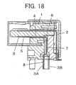
Patent Literature 1 discloses a multipolar connector in which a plurality ofupper contacts 2 and a plurality oflower contacts 3 are held by ahousing 1 made from an insulating resin and thelower contacts 3 include at least a pair of high-speed differentialsignal transmitting contacts FIG. 18 . - The high-speed differential
signal transmitting contacts portion 4 press-fitted and fixed in thehousing 1, a contactingportion 5 extending in a fitting direction of the connector, being exposed in front of thehousing 1 and being brought in contact with a contact of a counter connector, and an exposedportion 7 being exposed behind thehousing 1 and extending in a direction perpendicular to the fitting direction via abending portion 6. Ends of the exposedportions 7 of the high-speed differentialsignal transmitting contacts board connecting portions 8 that bend to be spaced apart from each other in the fitting direction and therefore have a staggered arrangement. - Patent Literature 1:
JP 2011-9151 A - In order to efficiently transmit high-speed differential signals, the impedances of the high-speed differential
signal transmitting contacts - In impedance matching, however, when the length of the press-fitted
portion 4 tightly adhered to thehousing 1 made from an insulting resin is increased, the dielectric loss increases while the impedance of the contact decreases, and accordingly, it is difficult to achieve the efficient transmission. - On the other hand, when the length of the press-fitted
portion 4 is decreased and the length of the exposedportion 7 which is not enclosed by thehousing 1 is increased, although the dielectric loss decreases, the impedance increases and cannot match with the predetermined value, accordingly. If the exposedportion 7 has an increased width to have a large capacity, the increase in impedance between the high-speed differentialsignal transmitting contacts portion 7 extending from thebending portion 6 in the direction perpendicular to the fitting direction, the height of the connector is increased, disadvantageously. - When, to cope with it, a modified contact is assumed in which the exposed
portion 7 not enclosed by thehousing 1 is located between the press-fittedportion 4 and thebending portion 6 to extend along the fitting direction and the exposedportion 7 is larger in width than the press-fittedportion 4, the dielectric loss decreases and also impedance matching is achieved without increasing the height of the connector. In such a contact, shoulders of the exposedportion 7 are formed because the wide exposedportion 7 joins thebending portion 6, and the shoulders are pressed by a jig to press-fit the press-fittedportion 4 into thehousing 1. At this time, since the exposedportion 7 is located between the press-fittedportion 4 and thebending portion 6 and this increases the distance from the shoulders of the exposedportion 7 to be pressed by the jig to the press-fittedportion 4, the buckling of the contact easily occurs in press-fitting. Even after the contact has been press-fitted, when an external force acts on theboard connecting portion 8 toward thebending portion 6 in, for example, connecting theboard connecting portion 8 to a board, the exposedportion 7 may deviate from the fitting direction and this prompts the contact to come off. - Such problems arise not only in paired contacts as described in
Patent Literature 1 but also in a contact for use in transmitting a signal other than a differential signal if impedance of the contact needs to match with a predetermined value set in advance and the contact is press-fitted in a housing made from a resin. Such a contact whose impedance needs to match with a predetermined value set in advance is hereinafter called "high-speed signal transmitting contact." - The present invention has been made to solve the conventional problems described above and is aimed at providing a connector with which impedance matching is achieved with the dielectric loss remaining low and which is capable of preventing a contact from buckling in press-fitting and from coming off after press-fitting.
- The present inventions provides a connector, comprising: a housing made from an insulating resin; and high-speed signal transmitting contacts arranged at and held by the housing, wherein each of all the high-speed signal transmitting contacts has at its one end a contacting portion to be brought in contact with a contact of a counter connector, at its another end a board connecting portion to be connected to a board, and a bending portion being located between the contacting portion and the board connecting portion, wherein a straight section extending from the contacting portion to the bending portion in a fitting direction with the counter connector is formed, the straight section having a press-fitted portion being adjacent to the contacting portion and being press-fitted into and fixed to the housing, an exposed portion being adjacent to the press-fitted portion, being exposed outside the housing and extending in the fitting direction, and a press-fitting shoulder portion being located between the exposed portion and the bending portion, wherein the board connecting portion extends from the bending portion in a direction intersecting the fitting direction, wherein the contacting portion has a width smaller than a width of the press-fitted portion, wherein the exposed portion has a width equal to or smaller than the width of the press-fitted portion, wherein the bending portion has a width smaller than a width of the press-fitting shoulder portion, and wherein the housing includes a resin wall extending throughout an entire length of the exposed portion in the fitting direction and facing a side surface of the exposed portion via an air layer, and an overhanging portion being connected to the resin wall and overhanging the exposed portion throughout the entire length of the exposed portion at an opposite side from a side facing in a direction in which the board connecting portion extends.
- Preferably, the resin wall is disposed between the exposed portions of a pair of the high-speed signal transmitting contacts adjacent to each other and has a height size larger than a thickness size of the exposed portion.
- The overhanging portion may overhang each of the exposed portions of the pair of high-speed signal transmitting contacts from an upper end of the resin wall.
- Preferably, the press-fitted portion has a projection projecting in a width direction.
- Preferably, the exposed portion has a width equal to or smaller than the width of the press-fitting shoulder portion.
- The press-fitting shoulder portion may have a pair of projections projecting separately on opposite sides in a width direction of the bending portion.
- Preferably, the board connecting portion extends in a direction perpendicular to the fitting direction.
- Each of all the high-speed signal transmitting contacts may have a wide portion being located between the bending portion and the board connecting portion, being exposed outside the housing and having a width larger than the width of the bending portion.
- It is preferable to further comprise a locator being fixed to the housing and serving to hold the board connecting portion of each of the high-speed signal transmitting contacts.
- The high-speed signal transmitting contacts may include at least a pair of differential signal contacts adjacent to each other for use in transmitting a high-speed differential signal, and the pair of differential signal contacts may be formed by bending metal plates of a same shape at the bending portions in a same direction and then bending the metal plates such that the board connecting portions are spaced apart from each other in the fitting direction so as to have a staggered arrangement.
- The contacting portion may or may not have spring properties.
- According to the present invention, the straight section extending in the fitting direction in the high-speed signal transmitting contact has the press-fitted portion being press-fitted into and fixed to the housing, the exposed portion being exposed outside the housing and extending in the fitting direction, and the press-fitting shoulder portion, the contacting portion has a width smaller than the width of the press-fitted portion, the exposed portion has a width equal to or smaller than the width of the press-fitted portion, the bending portion has a width smaller than the width of the press-fitting shoulder portion, and the housing includes the resin wall extending throughout the entire length of the exposed portion and facing a side surface of the exposed portion via the air layer, and an overhanging portion being connected to the resin wall and overhanging over the exposed portion throughout the entire length of the exposed portion at the opposite side from the side facing in the direction in which the board connecting portion extends. Owing to this configuration, impedance matching can be achieved with the dielectric loss remaining low, and a contact is prevented from buckling in press-fitting and from coming off after press-fitting.
-
- [
FIG. 1] FIG. 1 is a perspective view showing a receptacle connector according toEmbodiment 1 of the invention, when viewed from an obliquely front upper position. - [
FIG. 2] FIG. 2 is a perspective view showing the receptacle connector according toEmbodiment 1, when viewed from an obliquely rear upper position. - [
FIG. 3] FIG. 3 is a perspective view showing the receptacle connector according toEmbodiment 1, when viewed from an obliquely front lower position. - [
FIG. 4] FIG. 4 is a perspective view showing the receptacle connector according toEmbodiment 1, when viewed from an obliquely rear lower position. - [
FIG. 5] FIG. 5 is a plan view showing the receptacle connector according toEmbodiment 1. - [
FIG. 6] FIG. 6 is a cross-sectional view taken along line A-A ofFIG. 5 . - [
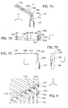
FIGS. 7] FIGS. 7A to FIG. 7D are respectively a perspective view, a plan view, a side view and a back view, all showing a pair of high-speed signal transmitting contacts used in the receptacle connector according toEmbodiment 1. - [
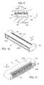
FIG. 8] FIG. 8 is an enlarged perspective view showing an important part of the receptacle connector according toEmbodiment 1. - [
FIG. 9] FIG. 9 is a partial enlarged cross-sectional view showing a region including an exposed portion, as well as its vicinity, of a high-speed signal transmitting contact in the receptacle connector according toEmbodiment 1. - [
FIG. 10] FIG. 10 is a perspective view showing a plug connector according toEmbodiment 2, when viewed from an obliquely front upper position. - [
FIG. 11] FIG. 11 is a perspective view showing the plug connector according toEmbodiment 2, when viewed from an obliquely rear upper position. - [
FIG. 12] FIG. 12 is a perspective view showing the plug connector according toEmbodiment 2, when viewed from an obliquely front lower position. - [
FIG. 13] FIG. 13 is a perspective view showing the plug connector according toEmbodiment 2, when viewed from an obliquely rear lower position. - [
FIG. 14] FIG. 14 is a plan view showing the plug connector according toEmbodiment 2. - [
FIG. 15] FIG. 15 is a cross-sectional view taken along line B-B ofFIG. 14 . - [
FIG. 16] FIG. 16 is a perspective view showing a pair of high-speed signal transmitting contacts used in the plug connector according toEmbodiment 2. - [
FIG. 17] FIG. 17 is a partial enlarged cross-sectional view showing a region including an exposed portion, as well as its vicinity, of a high-speed signal transmitting contact in the plug connector according toEmbodiment 2. - [
FIG. 18] FIG. 18 is a cross-sectional view of a conventional connector. - Embodiments of the present invention are described below based on the appended drawings.
-
FIGS. 1 to 4 each show the structure of areceptacle connector 11 according toEmbodiment 1. - The
receptacle connector 11 includes ahousing 12 extending in a direction perpendicular to a fitting axis C and made from an insulating resin, and a plurality ofcontacts 13 are arranged at and held by thehousing 12. - The
housing 12 includes ahousing body 12A and a hollow frame-shaped portion 12B which extends forward from thehousing body 12A along the fitting axis C and which is to be inserted into a counter connector (not shown). In each of thecontacts 13, oneend 13A protrudes in the frame-shaped portion 12B along the fitting axis C, the middle part is fixed to thehousing body 12A, and theother end 13B is exposed outside thehousing body 12A. - The
other ends 13B of thecontacts 13 extend in a direction perpendicular to the fitting axis C and also perpendicular to a direction in which thehousing 12 extends. Alocator 14 having a flat plate shape and serving to hold the other ends 13B of thecontacts 13 is fixed to thehousing 12. - For convenience, the direction in which the
contacts 13 are aligned and thehousing 12 extends is called "X direction," the direction along the fitting direction C from the front to the back of thehousing 12 "+Y direction," and the direction in which the other ends 13B of thecontacts 13 extend "-Z direction." - As shown in
FIG. 5 , the frame-shapedportion 12B of thehousing 12 protrudes from thehousing body 12A in the - Y direction, and thecontacts 13 are aligned in the X direction. -
FIG. 6 shows the cross-sectional structure of thereceptacle connector 11 as cut in a YZ plane passing through onecontact 13. Thehousing 12 includes acontact support portion 12C of flat plate shape extending along a XY plane at a Z direction position in the middle of the frame-shapedportion 12B in the Z direction at the +Y direction side with respect to thehousing body 12A, and thecontacts 13 are divided into two groups of a plurality ofupper contacts 15 which are aligned at the +Z direction side of thecontact support portion 12C and a plurality oflower contacts 16 which are aligned at the -Z direction side of thecontact support portion 12C. - The
upper contacts 15 are high-speed signal transmitting contacts, and for instance, each pair of contacts adjacent to each other constitutes a high-speed differential signal transmitting contact pair, so that a plurality of the high-speed differential signal transmitting contact pairs are provided. On the other hand, thelower contacts 16 are contacts for transmitting electric signals that are not high-speed signals (i.e., contacts whose impedances need not match with a predetermined value set in advance). - The
upper contacts 15 each include a contactingportion 15A positioned at the -Y direction-side end, a press-fittedportion 15B adjacent to the contactingportion 15A at the +Y direction side, an exposedportion 15C adjacent to the press-fittedportion 15B, a bendingportion 15D adjacent to the exposedportion 15C, awide portion 15E adjacent to the bendingportion 15D, and aboard connecting portion 15F adjacent to thewide portion 15E. Theupper contacts 15 are each provided with a straight section L1 extending from the contactingportion 15A to the bendingportion 15D in the Y direction that is the fitting direction. - The contacting
portion 15A is brought into contact with a contact of a counter connector (not shown) to establish the electric connection, has spring properties, and is exposed outside thehousing 12 and located in ahollow portion 12D of the frame-shapedportion 12B. - The press-fitted
portion 15B is press-fitted into a press-fittinghole 12E extending through thehousing body 12A in the Y direction to fix theupper contact 15 to thehousing 12. - The exposed
portion 15C is exposed outside thehousing 12 at the +Y direction side of thehousing body 12A and extends in the +Y direction that is the fitting direction. - The bending
portion 15D bends at a substantially right angle. Due to the bendingportion 15D present between the exposedportion 15C and thewide portion 15E, thewide portion 15E extends from the bendingportion 15D in the -Z direction. - The -Z direction-side end of the
wide portion 15E bends in the Y direction and is connected to theboard connecting portion 15F, and consequently, theboard connecting portion 15F extends in the -Z direction at a position where it is deviated from the +Z direction-side end of thewide portion 15E in the Y direction by a predetermined distance. - The
upper contacts 15 aligned in the X direction are configured so that the -Z direction-side ends of thewide portions 15E bend alternately toward the -Y direction and +Y direction and are then connected to the correspondingboard connecting portions 15F, and the +Z direction-side ends of theboard connecting portions 15F configured as above are inserted in through-holes 14A of thelocator 14, whereby theboard connecting portions 15F of theupper contacts 15 are held in a staggered arrangement. -
FIGS. 7A to 7D each show a pair ofupper contacts 15 constituting a high-speed differential signal transmitting contact pair. The pair ofupper contacts 15 are formed of two metal plates cut in the same shape. The two metal plates are curved in the same direction at the contactingportions 15A, bent in the same direction at the bendingportions 15D, bent in the opposite directions at thewide portions 15E and bent in the opposite directions at theboard connecting portions 15F, thereby forming the pair ofupper contacts 15 of the same shape except that the twoboard connecting portions 15F are shaped to be spaced apart in the Y direction that is the fitting direction. - In each of the
upper contacts 15, a press-fitting shoulder portion 15G having a pair of projections which project on the opposite sides in the width direction of the bendingportion 15D, namely, in the X direction is formed on the border between the exposedportion 15C and the bendingportion 15D. - The press-fitted
portion 15B has press-fitting projections which project on the opposite sides in the width direction, namely, in the X direction. - As shown in
FIG. 7B , when the widths of the contactingportion 15A, the press-fittedportion 15B including the press-fitting projections, the exposedportion 15C, the press-fitting shoulder portion 15G, the bendingportion 15D and thewide portion 15E are denoted by W1, W2, W3, W4, W5 and W6, respectively, the width W1 of the contactingportion 15A is set to be smaller than the width W2 of the press-fittedportion 15B including the press-fitting projections, and the width W5 of the bendingportion 15D is set to be smaller than the width W4 of the press-fitting shoulder portion 15G. - The width W3 of the exposed
portion 15C is set to be equal to or smaller than both of the width W2 of the press-fittedportion 15B and the width W4 of the press-fitting shoulder portion 15G, and the width W6 of thewide portion 15E is set to be larger than the width W5 of the bendingportion 15D. - As shown in
FIG. 8 , a plurality ofresin walls 12F are formed on the surface of thecontact support portion 12C of thehousing 12 at the +Z direction side so as to be each located between adjacentexposed portions 15C of theupper contacts 15. Theresin walls 12F each extend in the Y direction throughout the entire length of the exposedportion 15C of theupper contact 15. As shown inFIG. 9 , each wall surface of theresin wall 12F faces a side surface S1 of the exposedportion 15C via an air layer A1. Owing to the setting in which the width W3 of the exposedportion 15C is equal to or smaller than the width W2 of the press-fittedportion 15B, theresin wall 12F and the air layers A1 described above are allowed to be present between the exposedportions 15C of twoupper contacts 15 adjacent to each other. - In addition, an overhanging
portion 12G is formed at the +Z direction-side end of eachresin wall 12F to overhang the exposedportions 15C of twoupper contacts 15 located at both sides of theresin wall 12F and extend throughout the entire length of the exposedportion 15C at the +Z direction side of the exposedportions 15C, i.e., at the opposite side from the side facing in the -Z direction in which theboard connecting portions 15F extend. - The
resin wall 12F has a height size larger than the thickness size of the exposedportion 15C of theupper contact 15. As shown inFIG. 9 , the surface of the exposedportion 15C at the +Z direction side is in contact with the corresponding overhangingportions 12G, while the surface of the exposedportion 15C at the -Z direction side is away from the surface of thecontact support portion 12C at the +Z direction side so that an air layer B1 is formed between those surfaces. The degree of overhanging of each overhangingportion 12G in the X direction is set to a value which allows the overhangingportion 12G partially to overlap the exposedportion 15C of the relevantupper contact 15 in the Z direction, and a gap K1 is formed on the exposedportion 15C between a pair of overhangingportions 12G facing each other. - With the contacting
portion 15A being positioned at the +Y direction side of the press-fittinghole 12E of thehousing body 12A, the press-fitting shoulder portion 15G is pressed with a jig (not shown) in the -Y direction, and as a consequence, theupper contact 15 can be held in thehousing 12. At this time, owing to the setting in which the width W1 of the contactingportion 15A is smaller than the width W2 of the press-fittedportion 15B, the press-fittedportion 15B is press-fitted into the press-fittinghole 12E after the contactingportion 15A has been inserted into the press-fittinghole 12E, and consequently, theupper contact 15 is fixed to thehousing 12. - The exposed
portion 15C extending in the Y direction is present between the press-fittedportion 15B and the press-fitting shoulder portion 15G and therefore, the distance from the press-fitting shoulder portion 15G to be pressed by the jig to the press-fittedportion 15B to be press-fitted into the press-fittinghole 12E is long. However, since the overhangingportion 12G is formed at the +Z direction side of the exposedportion 15C throughout the entire length of the exposedportion 15C and the surface of thecontact support portion 12C is positioned at the -Z direction side of the exposedportion 15C via the air layer B1, the buckling of theupper contact 15 can be prevented. - In addition, the exposed
portion 15C of theupper contact 15 extending in the Y direction has the side surfaces S1 each of which faces the correspondingresin wall 12F via the air layer A1, the surface at the -Z direction side which faces the surface of thecontact support portion 12C via the air layer B1, and the surface at the +Z direction side on which the gap K1 is formed. Owing to this configuration, impedance matching of theupper contact 15 can be achieved with the dielectric loss remaining low. - The width W6 of the
wide portion 15E which is exposed outside thehousing 12 is set to be larger than the width W5 of the bendingportion 15D, and impedance matching can be achieved by adjusting the width W6 of thewide portion 15E. - As shown in
FIG. 6 , together with the thus configuredupper contacts 15, thelower contacts 16 are aligned at the -Z direction side of thecontact support portion 12C. - The
lower contacts 16 each include a contactingportion 16A that has spring properties and is positioned at the -Y direction-side end, a press-fittedportion 16B that is adjacent to the contactingportion 16A at the +Y direction side and is press-fitted into the press-fittinghole 12E of thehousing body 12A, a bendingportion 16C adjacent to the press-fittedportion 16B, and aboard connecting portion 16D adjacent to the bendingportion 16C, as with theupper contacts 15. - The
lower contacts 16 aligned in the X direction are each configured so that the length from the press-fittedportion 16B to the bendingportion 16C is set alternately to either of two different values, and theboard connecting portions 16D of thelower contacts 16 as configured above are inserted in through-holes 14A of thelocator 14, whereby theboard connecting portions 16D of thelower contacts 16 are held in a staggered arrangement. - The thus configured
receptacle connector 11 is mounted on a board (not shown) and used with theboard connecting portions 15F of theupper contacts 15 and theboard connecting portions 16D of thelower contacts 16 being connected to the corresponding interconnects in the board. - At this time, although the exposed
portion 15C extending in the Y direction is provided adjacent to the press-fittedportion 15B in each of theupper contacts 15 and this increases the length from the bendingportion 15D to the press-fittedportion 15B press-fitted into the press-fittinghole 12E, since the overhangingportion 12G is formed throughout the entire length of the exposedportion 15C at the +Z direction side of the exposedportion 15C, i.e., at the opposite side from the side facing in the -Z direction in which theboard connecting portion 15F extends, even if an external force acts in the +Z direction on theboard connecting portion 15F of theupper contact 15 in mounting of thereceptacle connector 11, the exposedportion 15C and the bendingportion 15D are prevented from deviating from the fitting direction, so that the contact will not come off. - In addition, the exposed
portion 15C of theupper contact 15 lies at the straight section L1 extending in the fitting direction, thereby obtaining thereceptacle connector 11 that is kept small in height in the Z direction. - In the
receptacle connector 11 according toEmbodiment 1, impedance matching of theupper contact 15 can be achieved with the dielectric loss remaining low, and in addition, since theboard connecting portions 15F of theupper contacts 15 are disposed in a staggered arrangement, the narrow pitch can be realized while minimizing skew which may occur in high-speed signal transmission. -
FIGS. 10 to 14 each show the structure of aplug connector 21 according toEmbodiment 2. Theplug connector 21 is to be fitted with thereceptacle connector 11 ofEmbodiment 1 and includes ahousing 22 which extends in a direction perpendicular to the fitting axis C and which is made from an insulating resin. A plurality ofcontacts 23 are arranged at and held by thehousing 22. - For the
plug connector 21 ofEmbodiment 2, an X direction, a Y direction and a Z direction are defined in accordance with those defined for thereceptacle connector 11 ofEmbodiment 1 with which theplug connector 21 is to be fitted. - The
housing 22 includes ahousing body 22A. Thehousing body 22A has formed therein acounter-connector receiving portion 22B of recess shape which opens toward the +Y direction and serves to receive the frame-shapedportion 12B of thereceptacle connector 11 which is a counter connector. In each of thecontacts 23, oneend 23A protrudes in thecounter-connector receiving portion 22B, the middle part is fixed to thehousing body 22A, and theother end 23B is exposed outside thehousing body 22A. - The other ends 23B of the
contacts 23 extend in the - Z direction, and alocator 24 having a flat plate shape and serving to hold the other ends 23B of thecontacts 23 is fixed to thehousing 22. -
FIG. 15 shows the cross-sectional structure of theplug connector 21 as cut in a YZ plane passing through onecontact 23. Thehousing 22 includes acontact support portion 22C of flat plate shape extending along a XY plane from the inside of thecounter-connector receiving portion 22B to a point at the -Y direction side of thehousing body 22A at a Z direction position in the middle of thecounter-connector receiving portion 22B in the Z direction, and thecontacts 23 are divided into two groups of a plurality ofupper contacts 25 which are aligned at the +Z direction side of thecontact support portion 22C and a plurality oflower contacts 26 which are aligned at the -Z direction side of thecontact support portion 22C. - Each of the
upper contacts 25 has the same configuration as theupper contact 15 used in thereceptacle connector 11 ofEmbodiment 1 except that a contactingportion 25A has no spring properties. Specifically, theupper contacts 25 are high-speed signal transmitting contacts, and for instance, each pair of contacts adjacent to each other constitutes a high-speed differential signal transmitting contact pair, so that a plurality of the high-speed differential signal transmitting contact pairs are provided. Theupper contacts 25 each include the contactingportion 25A, a press-fittedportion 25B, an exposedportion 25C, a bendingportion 25D, awide portion 25E and aboard connecting portion 25F, and are each provided with a straight section L2 extending from the contactingportion 25A to the bendingportion 25D in the Y direction that is the fitting direction. - The press-fitted
portion 25B is press-fitted into a press-fittinghole 22E in thehousing body 22A to fix theupper contact 25 to thehousing 22. - In the
upper contact 25, as shown inFIG. 16 , a press-fitting shoulder portion 25G having a pair of projections which project on the opposite sides in the width direction of the bendingportion 25D, namely, in the X direction is formed on the border between the exposedportion 25C and the bendingportion 25D. - As with the
upper contact 15 inEmbodiment 1, the width of the contactingportion 25A is set to be smaller than that of the press-fittedportion 25B, and the width of the bendingportion 25D is set to be smaller than that of the press-fitting shoulder portion 25G. - The width of the exposed
portion 25C is set to be equal to or smaller than both widths of the press-fittedportion 25B and the press-fitting shoulder portion 25G, and the width of thewide portion 25E is set to be larger than that of the bendingportion 25D. - As shown in
FIG. 17 , a plurality ofresin walls 22F are formed on the surface of thecontact support portion 22C of thehousing 22 at the +Z direction side so as to be each located between adjacentexposed portions 25C of theupper contacts 25. Theresin walls 22F each extend in the Y direction throughout the entire length of the exposedportion 25C of theupper contact 25. Each wall surface of theresin wall 22F faces a side surface S2 of the exposedportion 25C via an air layer A2. Owing to the setting in which the width of the exposedportion 25C is equal to or smaller than that of the press-fittedportion 25B, theresin wall 22F and the air layers A2 described above are allowed to be present between the exposedportions 25C of twoupper contacts 25 adjacent to each other. - In addition, an overhanging
portion 22G is formed at the +Z direction-side end of eachresin wall 22F to overhang the exposedportions 25C of twoupper contacts 25 located at both sides of theresin wall 22F and extend throughout the entire length of the exposedportions 25C at the +Z direction side of the exposedportions 25C, i.e., at the opposite side from the side facing in the -Z direction in which theboard connecting portions 25F extend. - The
resin wall 22F has a height size larger than the thickness size of the exposedportion 25C of theupper contact 25. The surface of the exposedportion 25C at the - Z direction side is in contact with the surface of thecontact support portion 22C at the +Z direction side, while the surface of the exposedportion 25C at the +Z direction side is away from the corresponding overhangingportions 22G in the -Z direction. The degree of overhanging of each overhangingportion 22G in the X direction is set to a value which allows the overhangingportion 22G to partially overlap the exposedportion 25C of the relevantupper contact 25 in the Z direction, and a gap K2 is formed between a pair of overhangingportions 22G facing each other. - With the contacting
portion 25A being positioned at the -Y direction side of the press-fittinghole 22E of thehousing body 22A, the press-fitting shoulder portion 25G is pressed with a jig (not shown) in the +Y direction, and as a consequence, theupper contact 25 can be held in thehousing 22. At this time, owing to the setting in which the width of the contactingportion 25A is smaller than that of the press-fittedportion 25B, the press-fittedportion 25B is press-fitted into the press-fittinghole 22E after the contactingportion 25A has been inserted into the press-fittinghole 22E, and consequently, theupper contact 25 is fixed to thehousing 22. - The exposed
portion 25C extending in the Y direction is present between the press-fittedportion 25B and the press-fitting shoulder portion 25G and therefore, the distance from the press-fitting shoulder portion 25G to be pressed by the jig to the press-fittedportion 25B to be press-fitted into the press-fittinghole 22E is long. However, since the surface of thecontact support portion 22C extends throughout the entire length of the exposedportion 25C at the -Z direction side of the exposedportion 25C and the overhangingportion 22G is disposed at the +Z direction side of the exposedportion 25C, the buckling of theupper contact 25 can be prevented. - In addition, the exposed
portion 25C of theupper contact 25 extending in the Y direction has the side surfaces S2 each of which faces the correspondingresin wall 22F via the air layer A2, and the surface at the +Z direction side on which the gap K2 is formed. Owing to this configuration, impedance matching of theupper contact 25 can be achieved with the dielectric loss remaining low. - Furthermore, impedance matching can be achieved by adjusting the width of the
wide portion 25E which is exposed outside thehousing 22. - As shown in
FIG. 15 , together with the thus configuredupper contacts 25, thelower contacts 26 are aligned at the -Z direction side of thecontact support portion 22C. - The
lower contacts 26 each include a contactingportion 26A having no spring properties, a press-fittedportion 26B press-fitted into the press-fittinghole 22E of thehousing body 22A, a bendingportion 26C, and aboard connecting portion 26D, as with theupper contacts 25. - The
lower contacts 26 aligned in the X direction are each configured so that the length from the press-fittedportion 26B to the bendingportion 26C is set alternately to either of two different values, and theboard connecting portions 26D of thelower contacts 26 are inserted in through-holes 24A of thelocator 24, whereby theboard connecting portions 26D of thelower contacts 26 are held in a staggered arrangement. - The thus configured
plug connector 21 is mounted on a board (not shown) and used with theboard connecting portions 25F of theupper contacts 25 and theboard connecting portions 26D of thelower contacts 26 being connected to the corresponding interconnects in the board. - At this time, although the exposed
portion 25C extending in the Y direction is provided adjacent to the press-fittedportion 25B in each of theupper contacts 25 and this increases the length from the bendingportion 25D to the press-fittedportion 25B press-fitted into the press-fittinghole 22E, since the overhangingportion 22G is formed throughout the entire length of the exposedportion 25C at the +Z direction side of the exposedportion 25C, i.e., at the opposite side from the side facing in the -Z direction in which theboard connecting portion 25F extends, even if an external force acts in the +Z direction on theboard connecting portion 25F of theupper contact 25 in mounting of theplug connector 21, the exposedportion 25C and the bendingportion 25D are prevented from deviating from the fitting direction, so that the contact will not come off. - In addition, the exposed
portion 25C of theupper contact 25 lies at the straight section L2 extending in the fitting direction, thereby obtaining theplug connector 21 that is kept small in height in the Z direction. - In the
plug connector 21 according toEmbodiment 2, impedance matching of theupper contact 25 can be achieved with the dielectric loss remaining low, and in addition, since theboard connecting portions 25F of theupper contacts 25 are disposed in a staggered arrangement, the narrow pitch can be realized while minimizing skew which may occur in high-speed signal transmission. - While in
Embodiments board connecting portions upper contacts board connecting portions - While in
Embodiments upper contacts lower contacts lower contacts upper contacts - Alternatively, all of the
upper contacts lower contacts - The contacting
portions 15A of theupper contacts 15 and the contactingportions 16A of thelower contacts 16 in thereceptacle connector 11 according toEmbodiment 1 have spring properties, and the contactingportions 25A of theupper contacts 25 and the contactingportions 26A of thelower contacts 26 in theplug connector 21 according toEmbodiment 2 have no spring properties. However, the contactingportions 25A of theupper contacts 25 and the contactingportions 26A of thelower contacts 26 in theplug connector 21 may have spring properties, and the contactingportions 15A of theupper contacts 15 and the contactingportions 16A of thelower contacts 16 in thereceptacle connector 11 may have no spring properties, in the opposite manner. - The present invention is applicable not only to a connector having contacts arranged in two arrays of upper and lower rows but also to a wide variety of connectors each having a plurality of high-speed signal transmitting contacts arranged in a housing regardless of the number of contacts.
-
- 1 housing, 2 upper contact, 3 lower contact, 3A, 3B high-speed differential signal transmitting contact, 4 press-fitted portion, 5 contacting portion, 6 bending portion, 7 exposed portion, 8 board connecting portion, 11 receptacle connector, 12, 22 housing, 13, 23 contact, 12A, 22A housing body, 12B frame-shaped portion, 12C, 22C contact support portion, 12D hollow portion, 12E, 22E press-fitting hole, 12F, 22F resin wall, 12G, 22G overhanging portion, 13A, 23A one end, 13B, 23B other end, 14, 24 locator, 14A, 24A through-hole, 15, 25 upper contact, 15A, 16A, 25A, 26A contacting portion, 15B, 16B, 25B, 26B press-fitted portion, 15C, 25C exposed portion, 15D, 16C, 25D, 26C bending portion, 15E, 25E wide portion, 15F, 16D, 25F, 26D board connecting portion, 15G, 25G press-fitting shoulder portion, 16, 26 lower contact, 21 plug connector, 22B counter-connector receiving portion, C fitting axis, L1, L2 straight section, W1 to W6 width, A1, A2, B1 air layer, S1, S2 side surface, K1, K2 gap
Claims (12)
- A connector, comprising:a housing made from an insulating resin; andhigh-speed signal transmitting contacts arranged at and held by the housing,wherein each of all the high-speed signal transmitting contacts has at its one end a contacting portion to be brought in contact with a contact of a counter connector, at its another end a board connecting portion to be connected to a board, and a bending portion being located between the contacting portion and the board connecting portion,wherein a straight section extending from the contacting portion to the bending portion in a fitting direction with the counter connector is formed, the straight section having a press-fitted portion being adjacent to the contacting portion and being press-fitted into and fixed to the housing, an exposed portion being adjacent to the press-fitted portion, being exposed outside the housing and extending in the fitting direction, and a press-fitting shoulder portion being located between the exposed portion and the bending portion,wherein the board connecting portion extends from the bending portion in a direction intersecting the fitting direction,wherein the contacting portion has a width smaller than a width of the press-fitted portion,wherein the exposed portion has a width equal to or smaller than the width of the press-fitted portion,wherein the bending portion has a width smaller than a width of the press-fitting shoulder portion, andwherein the housing includes a resin wall extending throughout an entire length of the exposed portion in the fitting direction and facing a side surface of the exposed portion via an air layer, and an overhanging portion being connected to the resin wall and overhanging the exposed portion throughout the entire length of the exposed portion at an opposite side from a side facing in a direction in which the board connecting portion extends.
- The connector according to claim 1, wherein the resin wall is disposed between the exposed portions of a pair of the high-speed signal transmitting contacts adjacent to each other and has a height size larger than a thickness size of the exposed portion.
- The connector according to claim 2, wherein the overhanging portion overhangs each of the exposed portions of the pair of high-speed signal transmitting contacts from an upper end of the resin wall.
- The connector according to any one of claims 1 to 3, wherein the press-fitted portion has a projection projecting in a width direction.
- The connector according to any one of claims 1 to 4, wherein the exposed portion has a width equal to or smaller than the width of the press-fitting shoulder portion.
- The connector according to any one of claims 1 to 5, wherein the press-fitting shoulder portion has a pair of projections projecting separately on opposite sides in a width direction of the bending portion.
- The connector according to any one of claims 1 to 6, wherein the board connecting portion extends in a direction perpendicular to the fitting direction.
- The connector according to any one of claims 1 to 7, wherein each of all the high-speed signal transmitting contacts has a wide portion being located between the bending portion and the board connecting portion, being exposed outside the housing and having a width larger than the width of the bending portion.
- The connector according to any one of claims 1 to 8, further comprising a locator being fixed to the housing and serving to hold the board connecting portion of each of the high-speed signal transmitting contacts.
- The connector according to any one of claims 1 to 9,
wherein the high-speed signal transmitting contacts include at least a pair of differential signal contacts adjacent to each other for use in transmitting a high-speed differential signal,
the pair of differential signal contacts being formed by bending metal plates of a same shape at the bending portions in a same direction and then bending the metal plates such that the board connecting portions are spaced apart from each other in the fitting direction so as to have a staggered arrangement. - The connector according to any one of claims 1 to 10, wherein the contacting portion has spring properties.
- The connector according to any one of claims 1 to 10, wherein the contacting portion has no spring properties.
Applications Claiming Priority (1)
| Application Number | Priority Date | Filing Date | Title |
|---|---|---|---|
| JP2015098905A JP6437382B2 (en) | 2015-05-14 | 2015-05-14 | connector |
Publications (2)
| Publication Number | Publication Date |
|---|---|
| EP3093925A1 true EP3093925A1 (en) | 2016-11-16 |
| EP3093925B1 EP3093925B1 (en) | 2018-09-12 |
Family
ID=55542520
Family Applications (1)
| Application Number | Title | Priority Date | Filing Date |
|---|---|---|---|
| EP16160704.9A Active EP3093925B1 (en) | 2015-05-14 | 2016-03-16 | Connector |
Country Status (5)
| Country | Link |
|---|---|
| EP (1) | EP3093925B1 (en) |
| JP (1) | JP6437382B2 (en) |
| KR (1) | KR101802171B1 (en) |
| CN (1) | CN106159510B (en) |
| TW (1) | TWI571016B (en) |
Cited By (2)
| Publication number | Priority date | Publication date | Assignee | Title |
|---|---|---|---|---|
| US10784605B2 (en) | 2017-12-05 | 2020-09-22 | Tyco Electronics Japan G.K. | Connector with a contact retained in a housing |
| EP3719938A1 (en) * | 2019-04-04 | 2020-10-07 | Iriso Electronics Co., Ltd. | Connector |
Families Citing this family (9)
| Publication number | Priority date | Publication date | Assignee | Title |
|---|---|---|---|---|
| WO2019084717A1 (en) * | 2017-10-30 | 2019-05-09 | Amphenol Fci Asia Pte Ltd | Low crosstalk card edge connector |
| US10418734B1 (en) | 2018-07-26 | 2019-09-17 | Te Connectivity Corporation | Contact assembly for a straddle mount connector |
| JP2020181778A (en) * | 2019-04-26 | 2020-11-05 | 日本圧着端子製造株式会社 | High-speed transmission connector |
| JP7265418B2 (en) * | 2019-05-31 | 2023-04-26 | 日本航空電子工業株式会社 | connector |
| CN111525315A (en) * | 2020-03-24 | 2020-08-11 | 苏州聚峦电子元器件有限公司 | A kind of interface unit |
| CN214849145U (en) * | 2020-05-13 | 2021-11-23 | 日本航空电子工业株式会社 | Connector with a locking member |
| EP4293834B1 (en) * | 2022-06-13 | 2024-08-07 | Rosenberger Hochfrequenztechnik GmbH & Co. KG | Electrical connector and electrical connection |
| JP2025019718A (en) * | 2023-07-28 | 2025-02-07 | 日本航空電子工業株式会社 | Angled Connector |
| KR102974302B1 (en) * | 2024-08-08 | 2026-06-09 | 에이치알에스코리아 주식회사 | Board to Board Connector For Crosstalk Reduction And Impedance Matching |
Citations (3)
| Publication number | Priority date | Publication date | Assignee | Title |
|---|---|---|---|---|
| GB2024539A (en) * | 1978-06-29 | 1980-01-09 | Bunker Ramo | Electrical Contact Assembly for Printed Circuit Board Connector |
| EP1950841A2 (en) * | 2007-01-24 | 2008-07-30 | Sumitomo Wiring Systems, Ltd. | A connector and assembling method therefor |
| JP2011009151A (en) | 2009-06-29 | 2011-01-13 | Hosiden Corp | Multipolar connector |
Family Cites Families (13)
| Publication number | Priority date | Publication date | Assignee | Title |
|---|---|---|---|---|
| JP2921248B2 (en) * | 1992-02-14 | 1999-07-19 | 日本電気株式会社 | connector |
| US5586915A (en) * | 1994-12-20 | 1996-12-24 | The Whitaker Corporation | Electrical connector with contacts at different insertion depths |
| JPH10261458A (en) * | 1997-03-19 | 1998-09-29 | Oki Densen Kk | High-speed transmission connector |
| JP2005026109A (en) * | 2003-07-03 | 2005-01-27 | Sumitomo Wiring Syst Ltd | Connector |
| TW200514305A (en) * | 2003-10-15 | 2005-04-16 | Comax Technology Inc | Contact terminal of connector |
| CN201117870Y (en) * | 2007-11-12 | 2008-09-17 | 富士康(昆山)电脑接插件有限公司 | electrical connector |
| JP5270242B2 (en) * | 2008-07-17 | 2013-08-21 | 富士通コンポーネント株式会社 | Balanced transmission connector |
| CN201438579U (en) * | 2009-07-13 | 2010-04-14 | 富士康(昆山)电脑接插件有限公司 | Electric connector |
| CN103117463A (en) * | 2011-11-16 | 2013-05-22 | 泰科资讯科技有限公司 | Display port connector and circuit board in coupling connection with the same |
| CN103545631B (en) * | 2012-07-09 | 2016-03-09 | 凡甲电子(苏州)有限公司 | Electric connector |
| JP2014060043A (en) * | 2012-09-18 | 2014-04-03 | Japan Aviation Electronics Industry Ltd | Connector |
| JP6039511B2 (en) * | 2013-07-17 | 2016-12-07 | 日本航空電子工業株式会社 | connector |
| CN204144494U (en) * | 2014-08-11 | 2015-02-04 | 香港商安费诺(东亚)有限公司 | Card Edge Connectors with Improved Terminal Impedance |
-
2015
- 2015-05-14 JP JP2015098905A patent/JP6437382B2/en active Active
-
2016
- 2016-03-01 TW TW105106153A patent/TWI571016B/en active
- 2016-03-16 EP EP16160704.9A patent/EP3093925B1/en active Active
- 2016-03-31 KR KR1020160039258A patent/KR101802171B1/en active Active
- 2016-04-07 CN CN201610212777.3A patent/CN106159510B/en active Active
Patent Citations (3)
| Publication number | Priority date | Publication date | Assignee | Title |
|---|---|---|---|---|
| GB2024539A (en) * | 1978-06-29 | 1980-01-09 | Bunker Ramo | Electrical Contact Assembly for Printed Circuit Board Connector |
| EP1950841A2 (en) * | 2007-01-24 | 2008-07-30 | Sumitomo Wiring Systems, Ltd. | A connector and assembling method therefor |
| JP2011009151A (en) | 2009-06-29 | 2011-01-13 | Hosiden Corp | Multipolar connector |
Cited By (3)
| Publication number | Priority date | Publication date | Assignee | Title |
|---|---|---|---|---|
| US10784605B2 (en) | 2017-12-05 | 2020-09-22 | Tyco Electronics Japan G.K. | Connector with a contact retained in a housing |
| US11646518B2 (en) | 2017-12-05 | 2023-05-09 | Tyco Electronics Japan G.K. | Connector with a contact retained in a housing |
| EP3719938A1 (en) * | 2019-04-04 | 2020-10-07 | Iriso Electronics Co., Ltd. | Connector |
Also Published As
| Publication number | Publication date |
|---|---|
| TW201644119A (en) | 2016-12-16 |
| CN106159510B (en) | 2018-01-30 |
| TWI571016B (en) | 2017-02-11 |
| CN106159510A (en) | 2016-11-23 |
| KR20160134477A (en) | 2016-11-23 |
| JP2016219101A (en) | 2016-12-22 |
| JP6437382B2 (en) | 2018-12-12 |
| EP3093925B1 (en) | 2018-09-12 |
| KR101802171B1 (en) | 2017-11-28 |
Similar Documents
| Publication | Publication Date | Title |
|---|---|---|
| EP3093925B1 (en) | Connector | |
| US10879635B2 (en) | Electrical connector | |
| TWI738170B (en) | First connector, second connector and connector assembly | |
| TWI411182B (en) | Multiposition rf connector | |
| US8167631B2 (en) | Card edge connector | |
| US9106024B2 (en) | Electrical connector with a metal plate for preventing electromagnetic interference | |
| US9461423B2 (en) | Electrical connector | |
| EP2624374A1 (en) | Connector and electronic device | |
| US9515406B2 (en) | Electrical connector with improved electrical contacts | |
| CN103081237B (en) | Connector | |
| US9318829B2 (en) | Power connector and power contact thereof with improved support member for supporting engaging arm | |
| US9142920B2 (en) | Connector with differential pairs | |
| CN108879137B (en) | Terminal block | |
| CN105098516A (en) | Interlayer type socket connector | |
| US20130323955A1 (en) | Connector terminal and card edge type connector including this connector terminal | |
| CN115051211B (en) | Terminal module and connector using the terminal module | |
| US7815468B2 (en) | Connector | |
| CN202678564U (en) | Multiple-contact connector | |
| US9755324B2 (en) | Contact including a plurality of connectable parts | |
| US20140080362A1 (en) | Connector | |
| JP2017174624A (en) | Coaxial connector | |
| CN106953195A (en) | Electric connector and electric connector assembly | |
| JP2017111931A (en) | Electrical connector for board connection | |
| US9601884B2 (en) | Connector | |
| US9054461B2 (en) | Electronic component |
Legal Events
| Date | Code | Title | Description |
|---|---|---|---|
| PUAI | Public reference made under article 153(3) epc to a published international application that has entered the european phase |
Free format text: ORIGINAL CODE: 0009012 |
|
| 17P | Request for examination filed |
Effective date: 20160316 |
|
| AK | Designated contracting states |
Kind code of ref document: A1 Designated state(s): AL AT BE BG CH CY CZ DE DK EE ES FI FR GB GR HR HU IE IS IT LI LT LU LV MC MK MT NL NO PL PT RO RS SE SI SK SM TR |
|
| AX | Request for extension of the european patent |
Extension state: BA ME |
|
| RBV | Designated contracting states (corrected) |
Designated state(s): AL AT BE BG CH CY CZ DE DK EE ES FI FR GB GR HR HU IE IS IT LI LT LU LV MC MK MT NL NO PL PT RO RS SE SI SK SM TR |
|
| REG | Reference to a national code |
Ref country code: DE Ref legal event code: R079 Ref document number: 602016005424 Country of ref document: DE Free format text: PREVIOUS MAIN CLASS: H01R0012720000 Ipc: H01R0013647700 |
|
| GRAP | Despatch of communication of intention to grant a patent |
Free format text: ORIGINAL CODE: EPIDOSNIGR1 |
|
| STAA | Information on the status of an ep patent application or granted ep patent |
Free format text: STATUS: GRANT OF PATENT IS INTENDED |
|
| RIC1 | Information provided on ipc code assigned before grant |
Ipc: H01R 12/72 20110101ALI20180314BHEP Ipc: H01R 13/6477 20110101AFI20180314BHEP Ipc: H01R 13/41 20060101ALI20180314BHEP |
|
| INTG | Intention to grant announced |
Effective date: 20180328 |
|
| GRAS | Grant fee paid |
Free format text: ORIGINAL CODE: EPIDOSNIGR3 |
|
| GRAA | (expected) grant |
Free format text: ORIGINAL CODE: 0009210 |
|
| STAA | Information on the status of an ep patent application or granted ep patent |
Free format text: STATUS: THE PATENT HAS BEEN GRANTED |
|
| AK | Designated contracting states |
Kind code of ref document: B1 Designated state(s): AL AT BE BG CH CY CZ DE DK EE ES FI FR GB GR HR HU IE IS IT LI LT LU LV MC MK MT NL NO PL PT RO RS SE SI SK SM TR |
|
| REG | Reference to a national code |
Ref country code: GB Ref legal event code: FG4D |
|
| REG | Reference to a national code |
Ref country code: CH Ref legal event code: EP |
|
| REG | Reference to a national code |
Ref country code: IE Ref legal event code: FG4D |
|
| REG | Reference to a national code |
Ref country code: DE Ref legal event code: R096 Ref document number: 602016005424 Country of ref document: DE |
|
| REG | Reference to a national code |
Ref country code: AT Ref legal event code: REF Ref document number: 1041696 Country of ref document: AT Kind code of ref document: T Effective date: 20181015 |
|
| REG | Reference to a national code |
Ref country code: NL Ref legal event code: MP Effective date: 20180912 |
|
| REG | Reference to a national code |
Ref country code: LT Ref legal event code: MG4D |
|
| PG25 | Lapsed in a contracting state [announced via postgrant information from national office to epo] |
Ref country code: LT Free format text: LAPSE BECAUSE OF FAILURE TO SUBMIT A TRANSLATION OF THE DESCRIPTION OR TO PAY THE FEE WITHIN THE PRESCRIBED TIME-LIMIT Effective date: 20180912 Ref country code: FI Free format text: LAPSE BECAUSE OF FAILURE TO SUBMIT A TRANSLATION OF THE DESCRIPTION OR TO PAY THE FEE WITHIN THE PRESCRIBED TIME-LIMIT Effective date: 20180912 Ref country code: RS Free format text: LAPSE BECAUSE OF FAILURE TO SUBMIT A TRANSLATION OF THE DESCRIPTION OR TO PAY THE FEE WITHIN THE PRESCRIBED TIME-LIMIT Effective date: 20180912 Ref country code: SE Free format text: LAPSE BECAUSE OF FAILURE TO SUBMIT A TRANSLATION OF THE DESCRIPTION OR TO PAY THE FEE WITHIN THE PRESCRIBED TIME-LIMIT Effective date: 20180912 Ref country code: GR Free format text: LAPSE BECAUSE OF FAILURE TO SUBMIT A TRANSLATION OF THE DESCRIPTION OR TO PAY THE FEE WITHIN THE PRESCRIBED TIME-LIMIT Effective date: 20181213 Ref country code: NO Free format text: LAPSE BECAUSE OF FAILURE TO SUBMIT A TRANSLATION OF THE DESCRIPTION OR TO PAY THE FEE WITHIN THE PRESCRIBED TIME-LIMIT Effective date: 20181212 Ref country code: BG Free format text: LAPSE BECAUSE OF FAILURE TO SUBMIT A TRANSLATION OF THE DESCRIPTION OR TO PAY THE FEE WITHIN THE PRESCRIBED TIME-LIMIT Effective date: 20181212 |
|
| PG25 | Lapsed in a contracting state [announced via postgrant information from national office to epo] |
Ref country code: HR Free format text: LAPSE BECAUSE OF FAILURE TO SUBMIT A TRANSLATION OF THE DESCRIPTION OR TO PAY THE FEE WITHIN THE PRESCRIBED TIME-LIMIT Effective date: 20180912 Ref country code: LV Free format text: LAPSE BECAUSE OF FAILURE TO SUBMIT A TRANSLATION OF THE DESCRIPTION OR TO PAY THE FEE WITHIN THE PRESCRIBED TIME-LIMIT Effective date: 20180912 Ref country code: AL Free format text: LAPSE BECAUSE OF FAILURE TO SUBMIT A TRANSLATION OF THE DESCRIPTION OR TO PAY THE FEE WITHIN THE PRESCRIBED TIME-LIMIT Effective date: 20180912 |
|
| REG | Reference to a national code |
Ref country code: AT Ref legal event code: MK05 Ref document number: 1041696 Country of ref document: AT Kind code of ref document: T Effective date: 20180912 |
|
| PG25 | Lapsed in a contracting state [announced via postgrant information from national office to epo] |
Ref country code: IT Free format text: LAPSE BECAUSE OF FAILURE TO SUBMIT A TRANSLATION OF THE DESCRIPTION OR TO PAY THE FEE WITHIN THE PRESCRIBED TIME-LIMIT Effective date: 20180912 Ref country code: CZ Free format text: LAPSE BECAUSE OF FAILURE TO SUBMIT A TRANSLATION OF THE DESCRIPTION OR TO PAY THE FEE WITHIN THE PRESCRIBED TIME-LIMIT Effective date: 20180912 Ref country code: ES Free format text: LAPSE BECAUSE OF FAILURE TO SUBMIT A TRANSLATION OF THE DESCRIPTION OR TO PAY THE FEE WITHIN THE PRESCRIBED TIME-LIMIT Effective date: 20180912 Ref country code: EE Free format text: LAPSE BECAUSE OF FAILURE TO SUBMIT A TRANSLATION OF THE DESCRIPTION OR TO PAY THE FEE WITHIN THE PRESCRIBED TIME-LIMIT Effective date: 20180912 Ref country code: RO Free format text: LAPSE BECAUSE OF FAILURE TO SUBMIT A TRANSLATION OF THE DESCRIPTION OR TO PAY THE FEE WITHIN THE PRESCRIBED TIME-LIMIT Effective date: 20180912 Ref country code: NL Free format text: LAPSE BECAUSE OF FAILURE TO SUBMIT A TRANSLATION OF THE DESCRIPTION OR TO PAY THE FEE WITHIN THE PRESCRIBED TIME-LIMIT Effective date: 20180912 Ref country code: IS Free format text: LAPSE BECAUSE OF FAILURE TO SUBMIT A TRANSLATION OF THE DESCRIPTION OR TO PAY THE FEE WITHIN THE PRESCRIBED TIME-LIMIT Effective date: 20190112 Ref country code: AT Free format text: LAPSE BECAUSE OF FAILURE TO SUBMIT A TRANSLATION OF THE DESCRIPTION OR TO PAY THE FEE WITHIN THE PRESCRIBED TIME-LIMIT Effective date: 20180912 Ref country code: PL Free format text: LAPSE BECAUSE OF FAILURE TO SUBMIT A TRANSLATION OF THE DESCRIPTION OR TO PAY THE FEE WITHIN THE PRESCRIBED TIME-LIMIT Effective date: 20180912 |
|
| PG25 | Lapsed in a contracting state [announced via postgrant information from national office to epo] |
Ref country code: SK Free format text: LAPSE BECAUSE OF FAILURE TO SUBMIT A TRANSLATION OF THE DESCRIPTION OR TO PAY THE FEE WITHIN THE PRESCRIBED TIME-LIMIT Effective date: 20180912 Ref country code: SM Free format text: LAPSE BECAUSE OF FAILURE TO SUBMIT A TRANSLATION OF THE DESCRIPTION OR TO PAY THE FEE WITHIN THE PRESCRIBED TIME-LIMIT Effective date: 20180912 Ref country code: PT Free format text: LAPSE BECAUSE OF FAILURE TO SUBMIT A TRANSLATION OF THE DESCRIPTION OR TO PAY THE FEE WITHIN THE PRESCRIBED TIME-LIMIT Effective date: 20190112 |
|
| REG | Reference to a national code |
Ref country code: DE Ref legal event code: R097 Ref document number: 602016005424 Country of ref document: DE |
|
| PLBE | No opposition filed within time limit |
Free format text: ORIGINAL CODE: 0009261 |
|
| STAA | Information on the status of an ep patent application or granted ep patent |
Free format text: STATUS: NO OPPOSITION FILED WITHIN TIME LIMIT |
|
| PG25 | Lapsed in a contracting state [announced via postgrant information from national office to epo] |
Ref country code: DK Free format text: LAPSE BECAUSE OF FAILURE TO SUBMIT A TRANSLATION OF THE DESCRIPTION OR TO PAY THE FEE WITHIN THE PRESCRIBED TIME-LIMIT Effective date: 20180912 |
|
| 26N | No opposition filed |
Effective date: 20190613 |
|
| PG25 | Lapsed in a contracting state [announced via postgrant information from national office to epo] |
Ref country code: SI Free format text: LAPSE BECAUSE OF FAILURE TO SUBMIT A TRANSLATION OF THE DESCRIPTION OR TO PAY THE FEE WITHIN THE PRESCRIBED TIME-LIMIT Effective date: 20180912 |
|
| PG25 | Lapsed in a contracting state [announced via postgrant information from national office to epo] |
Ref country code: MC Free format text: LAPSE BECAUSE OF FAILURE TO SUBMIT A TRANSLATION OF THE DESCRIPTION OR TO PAY THE FEE WITHIN THE PRESCRIBED TIME-LIMIT Effective date: 20180912 |
|
| REG | Reference to a national code |
Ref country code: CH Ref legal event code: PL |
|
| PG25 | Lapsed in a contracting state [announced via postgrant information from national office to epo] |
Ref country code: LU Free format text: LAPSE BECAUSE OF NON-PAYMENT OF DUE FEES Effective date: 20190316 |
|
| REG | Reference to a national code |
Ref country code: BE Ref legal event code: MM Effective date: 20190331 |
|
| PG25 | Lapsed in a contracting state [announced via postgrant information from national office to epo] |
Ref country code: IE Free format text: LAPSE BECAUSE OF NON-PAYMENT OF DUE FEES Effective date: 20190316 Ref country code: CH Free format text: LAPSE BECAUSE OF NON-PAYMENT OF DUE FEES Effective date: 20190331 Ref country code: LI Free format text: LAPSE BECAUSE OF NON-PAYMENT OF DUE FEES Effective date: 20190331 |
|
| PG25 | Lapsed in a contracting state [announced via postgrant information from national office to epo] |
Ref country code: FR Free format text: LAPSE BECAUSE OF NON-PAYMENT OF DUE FEES Effective date: 20190331 Ref country code: BE Free format text: LAPSE BECAUSE OF NON-PAYMENT OF DUE FEES Effective date: 20190331 |
|
| PG25 | Lapsed in a contracting state [announced via postgrant information from national office to epo] |
Ref country code: MT Free format text: LAPSE BECAUSE OF NON-PAYMENT OF DUE FEES Effective date: 20190316 |
|
| GBPC | Gb: european patent ceased through non-payment of renewal fee |
Effective date: 20200316 |
|
| PG25 | Lapsed in a contracting state [announced via postgrant information from national office to epo] |
Ref country code: GB Free format text: LAPSE BECAUSE OF NON-PAYMENT OF DUE FEES Effective date: 20200316 |
|
| PG25 | Lapsed in a contracting state [announced via postgrant information from national office to epo] |
Ref country code: CY Free format text: LAPSE BECAUSE OF FAILURE TO SUBMIT A TRANSLATION OF THE DESCRIPTION OR TO PAY THE FEE WITHIN THE PRESCRIBED TIME-LIMIT Effective date: 20180912 |
|
| PG25 | Lapsed in a contracting state [announced via postgrant information from national office to epo] |
Ref country code: HU Free format text: LAPSE BECAUSE OF FAILURE TO SUBMIT A TRANSLATION OF THE DESCRIPTION OR TO PAY THE FEE WITHIN THE PRESCRIBED TIME-LIMIT; INVALID AB INITIO Effective date: 20160316 |
|
| PG25 | Lapsed in a contracting state [announced via postgrant information from national office to epo] |
Ref country code: MK Free format text: LAPSE BECAUSE OF FAILURE TO SUBMIT A TRANSLATION OF THE DESCRIPTION OR TO PAY THE FEE WITHIN THE PRESCRIBED TIME-LIMIT Effective date: 20180912 |
|
| PGFP | Annual fee paid to national office [announced via postgrant information from national office to epo] |
Ref country code: DE Payment date: 20260128 Year of fee payment: 11 |
|
| PGFP | Annual fee paid to national office [announced via postgrant information from national office to epo] |
Ref country code: TR Payment date: 20260313 Year of fee payment: 11 |