EP3091683A1 - Rate dematching method, device and receiving-side apparatus - Google Patents
Rate dematching method, device and receiving-side apparatus Download PDFInfo
- Publication number
- EP3091683A1 EP3091683A1 EP14801749.4A EP14801749A EP3091683A1 EP 3091683 A1 EP3091683 A1 EP 3091683A1 EP 14801749 A EP14801749 A EP 14801749A EP 3091683 A1 EP3091683 A1 EP 3091683A1
- Authority
- EP
- European Patent Office
- Prior art keywords
- data
- sub
- bit
- code block
- subjected
- Prior art date
- Legal status (The legal status is an assumption and is not a legal conclusion. Google has not performed a legal analysis and makes no representation as to the accuracy of the status listed.)
- Granted
Links
Images






Classifications
-
- H—ELECTRICITY
- H04—ELECTRIC COMMUNICATION TECHNIQUE
- H04L—TRANSMISSION OF DIGITAL INFORMATION, e.g. TELEGRAPHIC COMMUNICATION
- H04L1/00—Arrangements for detecting or preventing errors in the information received
- H04L1/004—Arrangements for detecting or preventing errors in the information received by using forward error control
- H04L1/0056—Systems characterized by the type of code used
- H04L1/0067—Rate matching
-
- H—ELECTRICITY
- H04—ELECTRIC COMMUNICATION TECHNIQUE
- H04L—TRANSMISSION OF DIGITAL INFORMATION, e.g. TELEGRAPHIC COMMUNICATION
- H04L1/00—Arrangements for detecting or preventing errors in the information received
- H04L1/004—Arrangements for detecting or preventing errors in the information received by using forward error control
- H04L1/0056—Systems characterized by the type of code used
- H04L1/0071—Use of interleaving
-
- H—ELECTRICITY
- H04—ELECTRIC COMMUNICATION TECHNIQUE
- H04L—TRANSMISSION OF DIGITAL INFORMATION, e.g. TELEGRAPHIC COMMUNICATION
- H04L1/00—Arrangements for detecting or preventing errors in the information received
- H04L1/12—Arrangements for detecting or preventing errors in the information received by using return channel
- H04L1/16—Arrangements for detecting or preventing errors in the information received by using return channel in which the return channel carries supervisory signals, e.g. repetition request signals
- H04L1/18—Automatic repetition systems, e.g. Van Duuren systems
- H04L1/1812—Hybrid protocols; Hybrid automatic repeat request [HARQ]
-
- H—ELECTRICITY
- H04—ELECTRIC COMMUNICATION TECHNIQUE
- H04L—TRANSMISSION OF DIGITAL INFORMATION, e.g. TELEGRAPHIC COMMUNICATION
- H04L1/00—Arrangements for detecting or preventing errors in the information received
- H04L1/12—Arrangements for detecting or preventing errors in the information received by using return channel
- H04L1/16—Arrangements for detecting or preventing errors in the information received by using return channel in which the return channel carries supervisory signals, e.g. repetition request signals
- H04L1/18—Automatic repetition systems, e.g. Van Duuren systems
- H04L1/1829—Arrangements specially adapted for the receiver end
- H04L1/1835—Buffer management
- H04L1/1845—Combining techniques, e.g. code combining
Definitions
- the present invention relates to a field of communications, and particularly to a rate dematching method, apparatus and a receiving-side device.
- LTE Long Term Evolution
- 3G 3rd-Generation mobile communication
- MIMO multiple-input multiple-output
- a processing flow of a transmitting side (for a downlink traffic channel, the transmitting side is an eNodeB, and for an uplink traffic channel, the transmitting side is a user equipment (UE)) includes cyclic redundancy check (CRC)101, code block segmentation 102, Turbo encoding 103, rate matching 104, code block cascading 105, scrambling 106, modulation 107, layer mapping 108, pre-coding 109, resource mapping 110 and OFDM symbol generation 111.
- CRC cyclic redundancy check
- receiving processing flow of a receiving side includes reception of antenna data 201, demodulation of OFDM symbol 202, demodulation of MIMO 203, demodulation 204, descrambling 205, de-code-block decascading 206, rate dematching 207, hybrid automatic repeat request (HARQ) combination 208, decoding 209, de-CRC 210, etc.
- HARQ hybrid automatic repeat request
- the rate matching process structurally includes three interleaver sub-processes for respectively processing the three branches, one bit collection sub-process for summarization and one bit selection and clipping sub-process.
- Three branches of data are read into respectively independent sub-block interleavers in rows, NULL elements are filled in the front of an interleaving matrix with R rows and 32 columns, and data are read out in columns exchanged in columns.
- Rate dematching is a reverse process of the rate matching, and as shown in Figure 4 , a traditional rate dematching method includes bit recovery, bit separation and sub-block deinterleaving. The three processes are specifically realized as follows.
- Bit recovery includes:
- the bit separation corresponds to the bit collection of the rate matching.
- Data that have been subjected to bit recovery are read out of the circulating cache in sequence, and separated into three sub-blocks, wherein the first R ⁇ 32 data are written into a sub-block interleaver S, and the last 2 R ⁇ 32 data are alternately written into a sub-block de-interleaver P1 and a sub-block de-interleaver P2, and R is the number of rows of an interleaving matrix.
- sub-block deinterleaving data of three sub-blocks are respectively input in columns, switched in columns, and then output in rows, and the NULL elements added in sub-block interleaving are deleted when data are output.
- Rate dematching methods for LTE in an existing technology have problems of complex processing, huge hardware resource consumption and long processing time.
- embodiments of the present invention provide a rate dematching method, apparatus, and receiving-side device.
- Embodiments of the present invention provide a rate dematching method, including:
- the performing bit recovery/bit separation on the new data to be processed and writing data which have been subjected to bit recovery/bit separation into a code block data memory include:
- the code block data in the code block memory are stored in three branches which comprise system bits, a first parity bit and a second parity bit, and each branch of data is stored into two sub-memories according to a sequence in an interleaving matrix which has been subjected to the bit separation, that is, a first half part of each branch of data which have been subjected to bit separation is stored into one sub-memory, a second half part of each branch of data which have been subjected to bit separation is stored into another sub-memory, and the three branches of data are stored in a total of six sub-memories.
- the sub-block deinterleaving processing includes: calculating a sequence of the output data which have been subjected to sub-block interleaving, to obtain an address of the output data in the code block data memory, and reading data.
- the performing the bit recovery/bit separation on the new data to be processed and writing data which have been subjected to bit recovery/bit separation into the code block data memory include:
- the code block data memory is configured to store code block data in three branches which comprise system bits, a first parity bit and a second parity bit, and each branch of data is stored into two sub-memories according to a sequence in the interleaving matrix which has been subjected to the bit separation, that is, a first half part of each branch of data which have been subjected to bit separation is stored into one sub-memory, a second half part of each branch of data which have been subjected to bit separation is stored into another sub-memory, and the three branches of data are stored in a total of six sub-memories.
- the sub-block deinterleaving module is configured to calculate the sequence of the output data which have been subjected to sub-block interleaving according to the sequence of output data, to obtain the address of the output data in the code block data memory, and read data.
- Embodiments of the present invention also provide a receiving-side device for data communication, including the rate dematching apparatus of any one of the above-mentioned embodiments.
- Embodiments of the present invention also provide a computer readable storage medium, including a set of computer executable instructions for executing the method of any one of the above-mentioned rate dematching method of present invention.
- a rate dematching method, apparatus and a receiving-side device provided in embodiments of the present invention simplify processing complexity, reduce hardware resource consumption, and improve work efficiency.
- Embodiments of the present invention provide an apparatus and method for realizing rate dematching including HARQ combination for an LTE traffic channel.
- rate matching parameters and HARQ combination parameters of a transmission block (TB) are sent to the device by a system; the device reads new data to be processed and history data from the system through a data bus, and writes out HARQ combination results; and each data soft symbol occupies one byte.
- a rate dematching apparatus in an embodiment of the present invention includes a parameter processing and controlling module 501, a new data input module 502, de-repetition/de-punching module 503, sub-block deinterleaving module 504, a code block data memory 505, HARQ combination module 506, HARQ data input module 507 and HARQ data output module 508.
- the parameter processing and controlling module 501 is configured to acquire and distribute task parameters.
- the task parameters are in unit of TB. Further, the parameter processing and controlling module 501 parses the task parameters, divide the task parameters into code blocks (CB), and distribute the CBs to each of other modules.
- CB code blocks
- the new data input module 502 is configured to acquire and cache new data to be processed. NULL elements are not included in the new data. Further, the new data input module 502 reads data from outside through the data bus. A cache is set in the new data input module 502, and the cache mechanism is first input first output (FIFO). The new data input module 502 may read data by packets, and take data to process while reading, so that fewer storage resources are required.
- the de-repetition/de-punching module 503 is configured to perform bit recovery/bit separation. When processing each code block, the de-repetition/de-punching module 503 firstly clears the code block data memory, then reads data from the new data input module 502 and a code block data memory 505 simultaneously, combines data read from the new data input module 502 and a code block data memory 505, applies bit separation to combined data, and writes data which have been subjected to bit separation into the code block data memory 505.
- the de-repetition/de-punching module 503 adopts a 8-symbol parallel processing, naturally completes de-repetition/de-punching in a process of combination and writing data into the code block data memory 505, and the NULL elements are not required to be recovered.
- the sub-block deinterleaving module 504 is configured to apply sub-block deinterleaving.
- the sub-block deinterleaving module 504 calculates a sequence of output data which have been subjected to sub-block interleaving and reads three branches of data, i.e. system bits, a first parity bit and a second parity bit from a code block data memory 505, wherein each branch of data are read parallel in 2 symbols.
- the code block data memory 505 is configured to store code block data which have been subject to bit recovery/bit separation, and do not include the NULL elements, that is, data which have not been subjected to sub-block deinterleaving.
- the code block data memory stores code block data in three branches, i.e. system bits, the first parity bit and the second parity bit, and each branch of data is stored into two sub-RAMs which respectively store a half of the data of three branches.
- each of the sub-RAMs simultaneously reads one symbol data, thus (3 ⁇ 2)-symbol parallel processing of the sub-block deinterleaving module can be realized.
- Two sub-RAMs respectively store an upper half part and a lower half part of data of one branch of data which have been subjected to bit recovery/bit separation, denoted by up_ram and dw_ram.
- the sub-RAM storing upper half part of system bits is named sys_up_ram
- the sub-RAM storing lower half part of system bits is named sys_dw_ram
- the sub-RAMs storing the other two branches of data are named by analogy.
- a code block size K must be an integral multiple of 8, and a code block will increase by 4 symbols after Turbo encoding.
- each sub-RAM When K is odd time of 8, the storage capacity of each sub-RAM equals to 6 plus an integral multiple of 8, i.e., only 6 valid symbols are stored at the last address of sub-RAM. In this case, a data format stored in all sub-RAMs is shown in Figure 6 .
- the HARQ combination module 506 is configured to combine data output by the sub-block deinterleaving module 504 and the history data output by the HARQ data input module 507.
- the HARQ combination module 506 adopts (3 ⁇ 2)-symbol parallel processing.
- the HARQ data input module 507 is configured to acquire and cache history data to be processed.
- the HARQ data input module 507 may read data from outside through the data bus, and the cache may be set in the HARQ data input module 507.
- the cache mechanism in present embodiments is FIFO, data can be read by packets and taken to process while being read, which only requires fewer storage resources.
- the HARQ data output module 508 is configured to cache and output HARQ combination results.
- the HARQ data output module 508 may write data out through the data bus, and the cache may be set in the HARQ data output module 508.
- the cache mechanism in present embodiments is FIFO, data can be written out by packets, and data which have been subjected to HARQ combination can be stored while being written out, which only requires fewer storage resources.
- the parameter processing and controlling module 501, the new data input module 502 the de-repetition/de-punching module 503, the sub-block deinterleaving module 504, the HARQ combination module 506, the HARQ data input module 507 and the HARQ data output module 508 in embodiments of the present invention may be realized through an application specific integrated circuit (ASIC) or a field-programmable gate array (FPGA) of an rate dematching apparatus; and the code block data memory 505 may be realized through RAM of the rate dematching apparatus.
- ASIC application specific integrated circuit
- FPGA field-programmable gate array
- a processing flow diagram of a rate dematching method in embodiments of the present invention includes steps 801-805.
- a parameter processing and controlling module acquires a task parameter, calculates and processes the acquired task parameter, and distributes processed task parameter to other modules in code blocks.
- a new data input module acquires data to be processed from outside and temporarily stores the data, where the data begins with a starting address k 0 of code block rate matching output, NULL elements are not included, and the total amount of data of one code block is e symbols.
- the new data input module may initiate a read request to a data bus when there is a free space in an FIFO cache, and read data of one packet every time; and when a de-repetition/de-punching module requires data, data are taken from the FIFO cache, converted to a bit width of 8 symbols, and transmitted to the de-repetition/de-punching module.
- step 804 and step805 the de-repetition/de-punching module receives new code block data, and firstly clears code block data memory for the code block.
- each of sub-RMAs stores data only starting from the address 0 ⁇ ⁇ k / 2 + 2 8 ⁇ , so zero clearing code block data memory is only required to be performed on the part of RAM, and zero clearing 6 sub-RAMs is performed simultaneously.
- the de-repetition/de-punching module After a code block data memory is cleared, the de-repetition/de-punching module reads data to be processed from the new data input module according to a bit width of 8 symbols, and data read out are adjusted to be aligned in a storage format in RAM; and meanwhile, corresponding addresses of data in RAM are calculated, data in RAM are read from the address and combined with new data, data combined are written back to RAM, where the written address is the same as the read address.
- a de-repetition/de-punching diagram is shown in Figure 9 . When e new data of a whole code block are all combined and written back, processing of bit recovery and bit separation is completed.
- the de-repetition/de-punching process is divided into a plurality of sub-steps, i.e. steps 1001-1011.
- Step 1001 to step 1004 are used for adjusting format of new data taken from an input cache.
- step 1001 data are read from the input cache, where the data are denoted by fifo_dat and the upper bytes of the data are ahead.
- step 1003 system bits is separated from a parity bit, and after the separation, data are denoted by dat_sp_sel. Since the total number of system bits is ( k +4), system bits of dat_remove_k0 are required to be supplemented by 4 bytes of 0 at the last 8-byte position; and after data roll for each circle in a virtual cache, the valid data of dat_sp_sel has one more beat than the valid data of dat_remove_k0.
- data output by rate matching is in an alternate format of p1_p2. But during the rate matching, since a column of p2 in which a NULL element is inserted is different from that of p1 in which the NULL element is inserted, positions of bits which are deleted finally are different, causing a position of p1 and p2 exchanged to be a format of p2_p1.
- p1 is a NULL element
- p2 is valid data.
- data are output in this way, data are changed to be in a format of p2_p1 until the last parity bit.
- dat_sp_sel is required to be adjusted from data in a yellow position, positions of every two bytes data will be exchanged.
- step 1004 data of two sub-RAMs of each branch are separated and denoted by dat_ud_sel.
- k 0 may be in the system bits or in the parity bits
- the number of valid symbols of a last address of each of sub-RAMs may be 2 or 6
- a virtual cache may also roll during rate matching, and in various cases, the numbers of added zero bytes are different.
- the number of valid symbols in RAM is denoted by ram_dat_sum
- delay for dat_sp_sel data is denoted by dat_sp_sel_dly* , wherein * indicates the number of beats of delay.
- k 0 is not necessarily in up_ram.
- data are completed by a number of bytes of 0 in case of beginning from up_ram; with a number of bytes of 0 supplemented for dat_remove_k0 and dat_sp_sel, the data format of dat_ud_sel produced finally must be consistent with a data format stored in RAM.
- step 1005 a mark of valid data of dat_ud_sel denoted by dat_ud_sel_valid is calculated.
- the number of bytes 0 added in the processing course of ud separation is indicated with a counter ud_add_dat_cnt.
- 0 is added only when data are in dw_ram.
- k 0 is in p_dw_ram, 4 byte of 0 are added at the starting position.
- Valid data of each beat have 8 bytes. According to ud_add_dat_cnt/8, added beats of data of up_sel_dat relative to sp_sel_dat can be known. However, the number of added beats of data at dat_remove_k0 and dat_sp_sel is respectively calculated in steps 1002 and 1003, and dat_ud_sel_valid is obtained by accumulating the three.
- Steps 1006-1009 are used for calculating a position of data dat_ud_sel in RAM and reading data in RAM from the position.
- Data are stored in RAM by sub-blocks; a bit width of sub-RAMs is 8 symbols (8 bytes), and ( k /2+2) valid symbols are stored. 8-byte parallel processing is adopted for data processing.
- the valid data in RAM are numbered beginning with sys_up_ram in every 8 bytes.
- Figure 13 and Figure 14 reveals that sub-RAM of the data, addresses of data in sub-RAM and enabled bits can be calculated through number values. Finally, a datum of the storage structure in sub-RAM is adjusted as up_sel_dat, and a unit number value of up_sel_dat may be calculated, where the unit number is denoted by dat_ud_sel_cnt. Steps are as follows.
- step 1006 an initial number value of data dat_ud_sel is calculated. If data of full 8 bytes are stored in each sub-RAM, k0 [14:3] may be regarded as an initial unit number of input data. But in the processing course, zero adding processing is made on dat_remove_k0, i.e., the data firstly written into RAM is data before dat_remove_k0, causing the number to move forward; on the other hand, valid data is not fully written in the valid address of sub-RAM; fewer 0 may be added to each end of sub-RAM and parts of data are delayed to a next unit, causing the number to move backward; a true starting unit number is determined in combination of two influences. There are several cases as follows.
- step 1007 dat_ud_sel_cnt is calculated. An initial value is already obtained in step 1006, and whenever dat_ud_sel is valid, i.e., when dat_ud_sel_valid is 1, the dat_ud_sel_cnt is added by 1. The value of dat_ud_sel_cnt returns zero when the value of dat_ud_sel_cnt reaches a maximum. When a mantissa of ram_dat_sum is 2, the maximum value of dat_ud_sel_cnt is (6M-3), otherwise, the maximum value of dat_ud_sel_cnt is (6M-1).
- step 1009 data read from a RAM address obtained in step 1008 are denoted by dat_ram_rd.
- step 1010 dat_ram_rd and new data dat_ud_sel in an adjusted format are summed and a summing result is denoted by dat_comb_wb.
- step 1011 dat_comb_wb is written back to the RAM original position calculated in step 1008.
- an HARQ data input module acquires history data from outside and temporarily stores the history data.
- the data have been subjected to sub-block deinterleaving and include three branches which include system bits, first parity bit and second parity bit.
- the data do not include NULL elements.
- the HARQ input module can initiate a read request to a data bus when there is a spare space in an FIFO buffer, and read data of one packet every time.
- the data are taken from the FIFO buffer, converted to data having a bit width having 3 ⁇ 2 symbols.
- the data having a bit width having 3 ⁇ 2 symbols are transmitted to the HARQ combination module.
- the sub-block deinterleaving module calculates a sequence of output data which have been subjected to sub-block interleaving, concurrently reads three branches of new data from a code block data memory, where each branch of new data has 2 symbols, and the data read from a code block data memory are transmitted to the HARQ combination module.
- sub-block deinterleaving reads data from the code block data through an index j in a one-to-one correspondence i ⁇ j between index addresses before and after sub-block interleaving.
- the data are output to the position of an index i before interleaving so as to finish sub-block deinterleaving, i.e., adopting an interleaving read mode. So a key of sub-block deinterleaving is to realize transformation of interleaving indexes of i ⁇ j.
- an i th element in a CB before interleaving is denoted by a serial number of the i th element in a matrix before interleaving after adding a NULL element.
- i ' can be obtained by i and then j is obtained.
- the correction factor S is related to N D .
- the NULL elements are mixed in each column.
- a relationship among system bits, the correction factor S and the column number of the first parity bit and N D obtained from a column transformation relationship is shown in Figure 15 .
- the system bits and the parity bit are independent.
- de-interleaving operations are executed parallel on three branches of data.
- odd and even symbols of each branch are simultaneously processed. If odd and even symbols before interleaving exist in different sub-RAMs, degree of parallelism may be further increased.
- Each column of sub-block interleaving has 32 columns. Therefore, if the column number before interleaving is an even number, i is also an even number. Column transformation of LTE sub-block interlacing is shown in Figure 17 .
- the column numbers are less than or equal to 15 after the interleaving, i.e., at a first half part of the matrix; when i is an odd number, the column numbers are greater than or equal to 16 after the interleaving, i.e., at a second half part of the matrix.
- each branch of data is stored in an upper part and a lower part in a sequence before sub-block interleaving. Therefore, parity parallel processing is possible, and finally, 6-symbol parallel processing is achieved.
- a corresponding relation between each branch of data and sub-RAM is:
- Data which have been subjected to sub-block deinterleaving are firstly combined with the history data of the code block, the combined data are transmitted to a Turbo decoder and written to the outside for a next HARQ process.
- the history data come from the data bus, and the combined data are also written out through the data bus. Reading data from the bus and writing data to the bus are not necessarily continuous. Therefore, a processing pipeline of sub-block deinterleaving may be suspended at any time.
- the sub-block deinterleaving module adopts a data packet for unit operation, i.e., one sub-pack data are continuously taken from the code block memory every time and executed sub-block deinterleaving, and sub-packs are not suspended.
- the HARQ combination module is checked for a data request, and then a next sub-pack is processed.
- the HARQ combination module is required to initiate a data processing request to the sub-block deinterleaving module only when at least data of one sub-pack exist in the HARQ data input module and at least a vacant space for accommodating data of one sub-pack exists in the HARQ data output module.
- a request of a next sub-pack can be accepted when processing of one sub-pack is not finished.
- a history request counter is arranged for sub-block deinterleaving. Whenever a request is received, a length of the sub-pack is added. When the counter is not zero, an interleaving address can be calculated and data is read from the code block memory. When 3 ⁇ 2 symbols are processed once, the data counter decreases 1.
- the HARQ combination module reads the history data from the HARQ data input module, and combines the history data with output data of sub-block deinterleaving. Results are outputted to an external decoding module as well as the HARQ data output module. Whether applying HARQ combination and outputting combination results can be configured in task parameters for enhancing application flexibility of the apparatus in the system.
- the HARQ data output module temporarily stories the HARQ combination results and writes the HARQ combination results to the outside.
- the module converts data of bit width of 3 ⁇ 2 symbols inputted by the HARQ combination module into data of system bits width and writes the data into an FIFO buffer.
- the HARQ output module initiates a writing request to a data bus when there is adequate data in an FIFO buffer, and writes data of one packet every time; and when the FIFO buffer will be fully written, the HARQ combination module is notified to suspend operation for preventing FIFO overflow.
- step 810 when data of one code block is fully written, processing of the code block is finished. If the code block is a last code block in a rate dematching task, the task is finished; otherwise, a next code block continues to be processed.
- step 1901 new data to be processed are acquired, bit recovery/bit separation are performed on the new data to be processed, and data which have been subjected to bit recovery/bit separation are written into a code block data memory.
- step 1902 sub-block deinterleaving processing is applied to data stored in the code block data memory.
- step 1903 HARQ combination processing are applied to output data which have been subjected to sub-block deinterleaving processing and acquired history data to be processed, and HARQ combination results are outputted.
- embodiments of the present invention also provide a receiving-side device for data communication, including the rate dematching apparatus of any one of the above-mentioned embodiments.
- the receiving-side device may be eNodeB; and for a uplink traffic channel, the receiving-side device may be UE.
- Embodiments of the present invention also provide a computer readable storage medium, including a set of computer executable instructions for executing the rate dematching method of any one of the above-mentioned embodiments of the present invention.
Landscapes
- Engineering & Computer Science (AREA)
- Computer Networks & Wireless Communication (AREA)
- Signal Processing (AREA)
- Error Detection And Correction (AREA)
Abstract
Description
- The present invention relates to a field of communications, and particularly to a rate dematching method, apparatus and a receiving-side device.
- A Long Term Evolution (LTE) is an evolution of a 3rd-Generation mobile communication (3G) technology. LTE improves and enhances the air access technology of 3G. A new generation wireless networks based on orthogonal frequency division multiplexing (OFDM) and multiple-input multiple-output (MIMO) technologies can provide a peak rate of 100 Mbit/s in downlink and 50 Mbit/s in uplink under a spectral bandwidth of 20 MHZ, thereby improving the performance of cell edge users, increasing the cell capacity and spectrum utilization ratio and reducing the system delay. According to a technical standard 3GPP TS36.211/3GPP TS36.212 protocol file of the LTE, for the uplink and downlink traffic channels of the LTE, as shown in
Figure 1 , a processing flow of a transmitting side (for a downlink traffic channel, the transmitting side is an eNodeB, and for an uplink traffic channel, the transmitting side is a user equipment (UE)) includes cyclic redundancy check (CRC)101,code block segmentation 102,Turbo encoding 103, rate matching 104,code block cascading 105,scrambling 106,modulation 107,layer mapping 108, pre-coding 109,resource mapping 110 andOFDM symbol generation 111. As shown inFigure 2 , receiving processing flow of a receiving side (for the downlink traffic channel, the receiving side is an eNodeB, and for the uplink traffic channel, the receiving side is UE) includes reception ofantenna data 201, demodulation ofOFDM symbol 202, demodulation ofMIMO 203,demodulation 204, descrambling 205, de-code-block decascading 206,rate dematching 207, hybrid automatic repeat request (HARQ)combination 208,decoding 209, de-CRC 210, etc. - Each code block corresponds to one rate matching process, and the input of each rate matching is the output of the Turbo encoding, i.e., parallel three branches:


Figure 3 , the rate matching process structurally includes three interleaver sub-processes for respectively processing the three branches, one bit collection sub-process for summarization and one bit selection and clipping sub-process. Three branches of data are read into respectively independent sub-block interleavers in rows, NULL elements are filled in the front of an interleaving matrix with R rows and 32 columns, and data are read out in columns exchanged in columns. Then, the three branches of interleaved data


- Rate dematching is a reverse process of the rate matching, and as shown in
Figure 4 , a traditional rate dematching method includes bit recovery, bit separation and sub-block deinterleaving. The three processes are specifically realized as follows. - Bit recovery includes:
- 1. the following parameters are calculated: the length of each code block, the number Nd of NULL elements added in a sub-block interleaving of the rate matching, the length Ncb of a circulating cache, positions of the NULL elements in the circulating cache, a starting address k 0 of rate matching output, and the number e of physical channel bits of the code block;
- 2. starting from address k 0, data of an input sequence are input to the circulating cache in sequence; if a current address corresponds a NULL element, 0 is written into the circulating cache, otherwise, input data are written into the circulating cache; and when the address is increased to Ncb , the address is returned to 0; and
- 3. according to e and Ncb , a de-repetition or de-punching process, i.e., an reverse process of bit selection and clipping of the rate matching, is performed; wherein the de-repetition is combining data repeatedly sent in bit selection and clipping, and the de-punching is recovering data removed in bit selection and clipping to 0.
- The bit separation corresponds to the bit collection of the rate matching. Data that have been subjected to bit recovery are read out of the circulating cache in sequence, and separated into three sub-blocks, wherein the first R × 32 data are written into a sub-block interleaver S, and the last 2R×32 data are alternately written into a sub-block de-interleaver P1 and a sub-block de-interleaver P2, and R is the number of rows of an interleaving matrix.
- In sub-block deinterleaving, data of three sub-blocks are respectively input in columns, switched in columns, and then output in rows, and the NULL elements added in sub-block interleaving are deleted when data are output.
- Rate dematching methods for LTE in an existing technology have problems of complex processing, huge hardware resource consumption and long processing time.
- To solve the above-mentioned technical problems, embodiments of the present invention provide a rate dematching method, apparatus, and receiving-side device.
- Embodiments of the present invention provide a rate dematching method, including:
- acquiring new data to be processed, performing bit recovery/bit separation on the new data to be processed, and writing data which have been subjected to bit recovery/bit separation into a code block data memory;
- applying sub-block deinterleaving processing to data stored in the code block data memory; and
- applying hybrid automatic repeat request (HARQ) combination processing on output data which have been subjected to sub-block deinterleaving processing and the acquired history data to be processed, and outputting HARQ combination results.
- The performing bit recovery/bit separation on the new data to be processed and writing data which have been subjected to bit recovery/bit separation into a code block data memory include:
- when processing each code block, firstly zero clearing the code block data memory, then reading data from the code block data memory, combining data read from the code block memory and the new data acquired, applying bit separation to combined data, and writing data which have been subjected to bit separation into the code block data memory.
- The code block data in the code block memory are stored in three branches which comprise system bits, a first parity bit and a second parity bit, and each branch of data is stored into two sub-memories according to a sequence in an interleaving matrix which has been subjected to the bit separation, that is,
a first half part of each branch of data which have been subjected to bit separation is stored into one sub-memory, a second half part of each branch of data which have been subjected to bit separation is stored into another sub-memory, and the three branches of data are stored in a total of six sub-memories. - The sub-block deinterleaving processing includes: calculating a sequence of the output data which have been subjected to sub-block interleaving, to obtain an address of the output data in the code block data memory, and reading data.
- Embodiments of the present invention also provide a rate dematching apparatus including:
- a parameter processing and controlling module, configured to acquire a task parameter, parse and process the task parameter and distribute the task parameters to other modules;
- a new data input module, configured to acquire and cache new data to be processed;
- a de-repetition/de-punching module, configured to perform bit recovery/bit separation on the new data to be processed, and write data which have been subjected to bit recovery/bit separation into a code block data memory;
- a sub-block deinterleaving module, configured to apply sub-block deinterleaving processing to data stored in the code block data memory;
- a hybrid automatic repeat request (HARQ) data input module, configured to acquire and cache history data to be processed;
- an HARQ combination module, configured to combine data output by the sub-block deinterleaving module and the history data output by the HARQ data input module; and
- an HARQ data output module, configured to cache and output HARQ combination results.
- The performing the bit recovery/bit separation on the new data to be processed and writing data which have been subjected to bit recovery/bit separation into the code block data memory include:
- when processing each code block, by the de-repetition/de-punching module, firstly zero clearing the code block data memory, then reading data from the new data input module and the code block data memory simultaneously, and applying bit separation to combined data, and writing data which have been subjected to bit separation into the code block data memory.
- The code block data memory is configured to store code block data in three branches which comprise system bits, a first parity bit and a second parity bit, and each branch of data is stored into two sub-memories according to a sequence in the interleaving matrix which has been subjected to the bit separation, that is,
a first half part of each branch of data which have been subjected to bit separation is stored into one sub-memory, a second half part of each branch of data which have been subjected to bit separation is stored into another sub-memory, and the three branches of data are stored in a total of six sub-memories. - The sub-block deinterleaving module is configured to calculate the sequence of the output data which have been subjected to sub-block interleaving according to the sequence of output data, to obtain the address of the output data in the code block data memory, and read data.
- Embodiments of the present invention also provide a receiving-side device for data communication, including the rate dematching apparatus of any one of the above-mentioned embodiments.
- Embodiments of the present invention also provide a computer readable storage medium, including a set of computer executable instructions for executing the method of any one of the above-mentioned rate dematching method of present invention.
- A rate dematching method, apparatus and a receiving-side device provided in embodiments of the present invention simplify processing complexity, reduce hardware resource consumption, and improve work efficiency.
-
-
Figure 1 is a flow diagram showing a data processing of a transmitting side of an LTE traffic channel in the existing technology; -
Figure 2 is a flow diagram showing a data processing of a receiving side of an LTE traffic channel in the existing technology; -
Figure 3 is a processing diagram showing rate matching of a transmitting side of an LTE traffic channel in the existing technology; -
Figure 4 is a processing diagram showing rate dematching of a receiving side of an LTE traffic channel in the existing technology; -
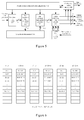
Figure 5 is a structure diagram showing a rate dematching apparatus in an embodiment of the present invention; -
Figure 6 is a diagram showing stored symbols of all sub-RAMs of a code block data memory when a code block size is odd time of 8 in an embodiment of the present invention; -
Figure 7 is a diagram showing stored symbols of all sub-RAMs of a code block data memory when a code block size is even time of 8 in an embodiment of the present invention; -
Figure 8 is a first processing flow diagram showing a method for rate dematching in an embodiment of the present invention; -
Figure 9 is a diagram showing de-repetition/de-punching in an embodiment of the present invention; -
Figure 10 is a processing flow diagram showing de-repetition/de-punching in an embodiment of the present invention; -
Figure 11 is a position diagram showing NULL elements before and after column transformation of system bits and a first parity bit data when nd=20 and R=4 in an embodiment of the present invention; -
Figure 12 is a position diagram showing NULL elements before and after column transformation of a second parity bit data when nd=20 and R=4 in an embodiment of the present invention; -
Figure 13 is a storage structure diagram showing addressing of all sub-RAMs according to a processing unit when the last three least significant bits (LSBs) of a number of valid symbols of sub-RAMs is 2 in an embodiment of the present invention; -
Figure 14 is a storage structure diagram showing addressing of all sub-RAMs according to a processing unit when the last three LSBs of a number of valid symbols of sub-RAMs is 6, in an embodiment of the present invention; -
Figure 15 is a diagram showing a relationship among a correction factor, a column number and ND in sub-block deinterleaving of system bits and a first parity bit in an embodiment of the present invention; -
Figure 16 is a diagram showing a relationship among a correction factor, a column number and ND in in sub-block deinterleaving of a second parity bit in an embodiment of the present invention; -
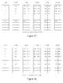
Figure 17 is a diagram showing column numbers of all columns before and after sub-block interleaving of system bits and a first parity bit in an embodiment of the present invention; -
Figure 18 a diagram showing column numbers of all columns before and after sub-block interleaving of a second parity bit in an embodiment of the present invention; and -
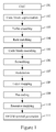
Figure 19 is a second processing flow diagram showing a rate dematching method in an embodiment of the present invention. - A technical solution of the present invention is described in detail below in combination with the drawings and the specific embodiments.
- Embodiments of the present invention provide an apparatus and method for realizing rate dematching including HARQ combination for an LTE traffic channel. In the embodiments, rate matching parameters and HARQ combination parameters of a transmission block (TB) are sent to the device by a system; the device reads new data to be processed and history data from the system through a data bus, and writes out HARQ combination results; and each data soft symbol occupies one byte.
- As shown in
Figure 5 , a rate dematching apparatus in an embodiment of the present invention includes a parameter processing and controllingmodule 501, a newdata input module 502, de-repetition/de-punching module 503,sub-block deinterleaving module 504, a codeblock data memory 505,HARQ combination module 506, HARQdata input module 507 and HARQdata output module 508. - The parameter processing and controlling
module 501 is configured to acquire and distribute task parameters. The task parameters are in unit of TB. Further, the parameter processing and controllingmodule 501 parses the task parameters, divide the task parameters into code blocks (CB), and distribute the CBs to each of other modules. - The new
data input module 502 is configured to acquire and cache new data to be processed. NULL elements are not included in the new data. Further, the newdata input module 502 reads data from outside through the data bus. A cache is set in the newdata input module 502, and the cache mechanism is first input first output (FIFO). The newdata input module 502 may read data by packets, and take data to process while reading, so that fewer storage resources are required. - The de-repetition/
de-punching module 503 is configured to perform bit recovery/bit separation. When processing each code block, the de-repetition/de-punching module 503 firstly clears the code block data memory, then reads data from the newdata input module 502 and a codeblock data memory 505 simultaneously, combines data read from the newdata input module 502 and a codeblock data memory 505, applies bit separation to combined data, and writes data which have been subjected to bit separation into the codeblock data memory 505. The de-repetition/de-punching module 503 adopts a 8-symbol parallel processing, naturally completes de-repetition/de-punching in a process of combination and writing data into the codeblock data memory 505, and the NULL elements are not required to be recovered. - The
sub-block deinterleaving module 504 is configured to apply sub-block deinterleaving. Thesub-block deinterleaving module 504 calculates a sequence of output data which have been subjected to sub-block interleaving and reads three branches of data, i.e. system bits, a first parity bit and a second parity bit from a codeblock data memory 505, wherein each branch of data are read parallel in 2 symbols. - The code
block data memory 505 is configured to store code block data which have been subject to bit recovery/bit separation, and do not include the NULL elements, that is, data which have not been subjected to sub-block deinterleaving. The code block data memory stores code block data in three branches, i.e. system bits, the first parity bit and the second parity bit, and each branch of data is stored into two sub-RAMs which respectively store a half of the data of three branches. Storage capacity of sub-RAM shall be greater than half of size of a maximum code block, i.e. 6148/2=3074. In order to cooperate with 8-symbol parallel processing of the de-repetition/de-punching module 503, a bit width of sub-RAM is 8 symbols, and a depth of sub-RAM is 3074/8=385. By using a single port RAM, each of the sub-RAMs simultaneously reads one symbol data, thus (3×2)-symbol parallel processing of the sub-block deinterleaving module can be realized. - Two sub-RAMs respectively store an upper half part and a lower half part of data of one branch of data which have been subjected to bit recovery/bit separation, denoted by up_ram and dw_ram. The sub-RAM storing upper half part of system bits is named sys_up_ram, and the sub-RAM storing lower half part of system bits is named sys_dw_ram, and the sub-RAMs storing the other two branches of data are named by analogy. According to 3GPP TS36.212, a code block size K must be an integral multiple of 8, and a code block will increase by 4 symbols after Turbo encoding. When K is odd time of 8, the storage capacity of each sub-RAM equals to 6 plus an integral multiple of 8, i.e., only 6 valid symbols are stored at the last address of sub-RAM. In this case, a data format stored in all sub-RAMs is shown in
Figure 6 . When K is even time of 8, the storage capacity of each ofsub-RAMs pluses 2 on the basis of an integral multiple of 8, i.e., the last address of sub-RAM only stores 6 valid symbols, and in this case, a data format stored in all sub-RAMs are shown inFigure 7 . - The
HARQ combination module 506 is configured to combine data output by thesub-block deinterleaving module 504 and the history data output by the HARQdata input module 507. TheHARQ combination module 506 adopts (3×2)-symbol parallel processing. - The HARQ
data input module 507 is configured to acquire and cache history data to be processed. The HARQdata input module 507 may read data from outside through the data bus, and the cache may be set in the HARQdata input module 507. The cache mechanism in present embodiments is FIFO, data can be read by packets and taken to process while being read, which only requires fewer storage resources. - The HARQ
data output module 508 is configured to cache and output HARQ combination results. The HARQdata output module 508 may write data out through the data bus, and the cache may be set in the HARQ data output module 508.The cache mechanism in present embodiments is FIFO, data can be written out by packets, and data which have been subjected to HARQ combination can be stored while being written out, which only requires fewer storage resources. - It is noted that the parameter processing and controlling
module 501, the newdata input module 502 the de-repetition/de-punching module 503, thesub-block deinterleaving module 504, theHARQ combination module 506, the HARQdata input module 507 and the HARQdata output module 508 in embodiments of the present invention may be realized through an application specific integrated circuit (ASIC) or a field-programmable gate array (FPGA) of an rate dematching apparatus; and the codeblock data memory 505 may be realized through RAM of the rate dematching apparatus. - As shown in
Figure 8 , a processing flow diagram of a rate dematching method in embodiments of the present invention includes steps 801-805. - In
step 801 and step 802, a parameter processing and controlling module, acquires a task parameter, calculates and processes the acquired task parameter, and distributes processed task parameter to other modules in code blocks. - In
step 803, a new data input module acquires data to be processed from outside and temporarily stores the data, where the data begins with a starting address k 0 of code block rate matching output, NULL elements are not included, and the total amount of data of one code block is e symbols. The new data input module may initiate a read request to a data bus when there is a free space in an FIFO cache, and read data of one packet every time; and when a de-repetition/de-punching module requires data, data are taken from the FIFO cache, converted to a bit width of 8 symbols, and transmitted to the de-repetition/de-punching module. - In
step 804 and step805, the de-repetition/de-punching module receives new code block data, and firstly clears code block data memory for the code block. As shown inFigure 6 andFigure 7 , each of sub-RMAs stores data only starting from theaddress 
clearing 6 sub-RAMs is performed simultaneously. - After a code block data memory is cleared, the de-repetition/de-punching module reads data to be processed from the new data input module according to a bit width of 8 symbols, and data read out are adjusted to be aligned in a storage format in RAM; and meanwhile, corresponding addresses of data in RAM are calculated, data in RAM are read from the address and combined with new data, data combined are written back to RAM, where the written address is the same as the read address. A de-repetition/de-punching diagram is shown in
Figure 9 . When e new data of a whole code block are all combined and written back, processing of bit recovery and bit separation is completed. - As shown in
Figure 10 , the de-repetition/de-punching process is divided into a plurality of sub-steps, i.e. steps 1001-1011. -
Step 1001 to step 1004 are used for adjusting format of new data taken from an input cache. - In
step 1001, data are read from the input cache, where the data are denoted by fifo_dat and the upper bytes of the data are ahead. - In
step 1002, fifo_dat beginning from (k0-k0[2:0]) are aligned according to a whole 8-byte, i.e., if k0[2:0]!=0, zero padding is applied to a lower byte, and data begin to be generated at a whole 8-byte; and the data are denoted by dat_remove_k0, and the valid data of dat_remove_k0 are more than one beat compared with the valid data of fifo_dat. - In
step 1003, system bits is separated from a parity bit, and after the separation, data are denoted by dat_sp_sel. Since the total number of system bits is (k+4), system bits of dat_remove_k0 are required to be supplemented by 4 bytes of 0 at the last 8-byte position; and after data roll for each circle in a virtual cache, the valid data of dat_sp_sel has one more beat than the valid data of dat_remove_k0. - For a parity bit, data output by rate matching is in an alternate format of p1_p2. But during the rate matching, since a column of p2 in which a NULL element is inserted is different from that of p1 in which the NULL element is inserted, positions of bits which are deleted finally are different, causing a position of p1 and p2 exchanged to be a format of p2_p1.
-
Figure 11 andFigure 12 explain situations of exchanging sequences of p1/p2 using the number of NULL elements of nd=20 and R=4 as an example, and bold italics in theFigure 11 andFigure 12 indicate serial numbers of NULL elements, and other numbers indicate serial numbers of valid data. In a shadow position ofFigure 12 , p1 is a NULL element, and p2 is valid data. When data are output in this way, data are changed to be in a format of p2_p1 until the last parity bit. When dat_sp_sel is required to be adjusted from data in a yellow position, positions of every two bytes data will be exchanged. - In
step 1004, data of two sub-RAMs of each branch are separated and denoted by dat_ud_sel. k 0 may be in the system bits or in the parity bits, the number of valid symbols of a last address of each of sub-RAMs may be 2 or 6, a virtual cache may also roll during rate matching, and in various cases, the numbers of added zero bytes are different. The number of valid symbols in RAM is denoted by ram_dat_sum, and delay for dat_sp_sel data is denoted by dat_sp_sel_dly* , wherein * indicates the number of beats of delay. There are several cases in the following. - In case (1), k 0 is in system bits and ram_dat_sum[2:0]=2, and rolling has not yet been executed:
- in sys_up_ram, dat_ud_sel <= sp_sel_dat_dly1;
- 6 bytes of 0 are added to the end of sys_up_ram, and dat_ud_sel <= {sp_sel_dat_dly1[63:48], 48'd0};
- in sys_dw_ram, 6 bytes of 0 have been added, and dat_ud_sel <= {sp_sel_dat_dly2[47:0], sp_sel_dat_dly1[63:48};
- 6 bytes of 0 shall have been added to an end of sys_dw_ram, but 4 bytes of 0 have already been added in sp separation before, therefore only 2 bytes of 0 are added to an end of sys_dw_ram here, and dat_ud_sel <= {sp_sel_dat_dly2[47:0], 16'd0};
- in p_up_ram, 8 bytes of 0 have been added before, i.e., delay by one beat, dat_ud_sel <= sp_sel_dat_dly2;
- at the end of p_up_ram, (k+4) data are stored in p_up_ram; finally, there are four valid data and four added bytes of 0 in the end of p_up_ram; dat_ud_sel <= {sp_sel_dat_dly2[63:32], 32'd0};
- in p_dw_ram, 12 bytes of 0 have been added before; dat_ud_sel <= {sp_sel_dat_dly3[31:0], sp_sel_dat_dly2[63:32]};
- 4 bytes of 0 are added to the end of p_dw_ram; dat_ud_sel <= {sp_sel_dat_dly3[31:0], 32'd0};
- in sys_up_ram which has been subjected to the first roll, 16 bytes of 0 have been added before, i.e., delay by two beats; dat_ud_sel <= sp_sel_dat_dly3;
- In case (2), k 0 is in system bits and ram_dat_sum[2:0]=6, and rolling has not yet been executed:
- in sys_up_ram, dat_ud_sel <= sp_sel_dat_dlyl;
- 2 bytes of 0 are added to the end of sys_up_ram, and dat_ud_sel <= {sp_sel_dat_dly1[63:16], 16'd0};
- in sys_dw_ram, 2 bytes of 0 have been added, and dat_ud_sel <= {sp_sel_dat_dly2[15:0] and sp_sel_dat_dly1[63:16};
- 2 bytes of 0 shall have been added to an end of sys_dw_ram, but 4 bytes of 0 have been already added in sp separation before, therefore 0 is not required to be added to an end of sys_dw_ram here, and dat_ud_sel <= {sp_sel_dat_dly2[15:0], sp_sel_dat_dly1[63:16}; 0 added herein is offset;
- in p_up_ram, 0 has not been added before; dat_ud_sel <= sp_sel_dat_dlyl;
- at the end of p_up_ram, (k+4) data are stored in p_up_ram, finally, there are four valid data, four bytes of 0 are added and dat_ud_sel <= {sp_sel_dat_dly1[63:32], 32'd0};
- in p_dw_ram, 4 bytes of 0 have been added before; dat_ud_sel <= {sp_sel_dat_dly2[31:0], sp_sel_dat_dly1[63:32]};
- 4 bytes of 0 are added to an end of p_dw_ram,; dat_ud_sel <= {sp_sel_dat_dly2[31:0], 32'd0};and
- in sys_up_ram which has been subjected to the first roll, 8 bytes of 0 have been added before, i.e., delay by one beat; dat_ud_sel <= sp_sel_dat_dly2.
- In case (3), k 0 is in parity bits and ram_dat_sum[2:0]=2, and rolling has not yet been executed:
- in p_up_ram, dat_ud_sel <= sp_sel_dat_dlyl;
- at an end of p_up_ram, (k+4) symbols are stored in p_up_ram; finally, there are four valid symbols, 4 bytes of 0 are added; dat_ud_sel <= {sp_sel_dat_dly1[63:32], 32'd0};
- in p_dw_ram, 4 bytes of 0 have been added before, and dat_ud_sel <= {sp_sel_dat_dly2[31:0], sp_sel_dat_dly1[63:32]};
- at the end of p_dw_ram, 4 bytes of 0 are added; dat_ud_sel <= {sp_sel_dat_dly2[31:0], 32'd0};
- in sys_up_ram which has been subjected to first roll, 8 bytes of 0 have been added before, i.e., delay by one beat; dat_ud_sel <= sp_sel_dat_dly2;
- at the end of sys_up_ram which has been subjected to first roll, 6 bytes of 0 are added, and dat_ud_sel <= {sp_sel_dat_dly2[63:48], 48'd0};
- in sys_dw_ram which has been subjected to first roll, 14 bytes of 0 have been added before, and dat_ud_sel <= {sp_sel_dat_dly3[47:0], sp_sel_dat_dly2[63:48]};
- at the end of sys_dw_ram which has been subjected to first roll, 6 bytes of 0 shall be added here, but 4 bytes of 0 have been added in sp separation, therefore 2 bytes of 0 are added, and dat_ud_sel <= {sp_sel_dat_dly3[47:0], 16'd0};
- at the end of p_up_ram which has been subjected to first roll, 16 bytes of 0 have been added before, dat_ud_sel <= sp_sel_dat_dly3.
- Then the above process is repeated; and two beats are added for each roll delay.
- In case (4), k 0 is in parity bits and ram_dat_sum[2:0]=6, and rolling has not yet been executed:
- in p_up_ram, dat_ud_sel <= sp_sel_dat_dlyl;
- at the end of p_up_ram, (k+4) symbols are stored in p_up_ram, finally, there are four valid symbols, 4 bytes of 0 are added, and dat_ud_sel <= {sp_sel_dat_dly1[63:32], 32'd0};
- in p_dw_ram, 4 bytes of 0 have been added before, and dat_ud_sel <= {sp_sel_dat_dly2[31:0], sp_sel_dat_dly1[63:32]};
- at the end of p_dw_ram, 4 bytes of 0 are added; dat_ud_sel <= {sp_sel_dat_dly2[31:0], 32'd0};
- in sys_up_ram which has been subjected to first roll, 8 bytes of 0 have been added before, i.e., delay by one beat, and dat_ud_sel <= sp_sel_dat_dly2;
- at the end of sys_up_ram which has been subjected to first roll, 2 bytes of 0 are added, and dat_ud_sel <= { sp_sel_dat_dly2[63:16], 16'd0};
- in sys_dw_ram which has been subjected to first roll, 10 bytes of 0 have been added before, and dat_ud_sel <= { sp_sel_dat_dly3[15:0], sp_sel dat_dly2[63:16]};
- at the end of sys_dw_ram which has been subjected to first roll, 2 bytes of 0 shall be added here, but 4 bytes of 0 have been added in sp separation, therefore 0 is not required to be added, and dat_ud_sel <= { sp_sel_dat_dly3[15:0], sp_sel_dat_dly2[63:16] }; 8
bytes 0 are in total added herein; - at the end of p_up_ram which has been subjected to first winding, 8 bytes of 0 have been added before, dat_ud_sel <= sp_sel_dat_dly2.
- Then the above process is repeated; and one beat is added for each winding delay.
- In practice, k 0 is not necessarily in up_ram. However, in the above processing, even if beginning from dw_ram, data are completed by a number of bytes of 0 in case of beginning from up_ram; with a number of bytes of 0 supplemented for dat_remove_k0 and dat_sp_sel, the data format of dat_ud_sel produced finally must be consistent with a data format stored in RAM.
- In
step 1005, a mark of valid data of dat_ud_sel denoted by dat_ud_sel_valid is calculated. - The number of
bytes 0 added in the processing course of ud separation is indicated with a counter ud_add_dat_cnt. - At the starting position, 0 is added only when data are in dw_ram. When k 0 is in sys_dw_ram, if ram_dat_sum [2:0]=2, 6 bytes of 0 are added at the starting position; and if ram_dat_sum [2:0]=6, 2 bytes of 0 are added at the starting position. When k 0 is in p_dw_ram, 4 byte of 0 are added at the starting position.
- In the data processing course, if ram_dat_sum [2:0]=2, 6 bytes of 0 are added at each end of sys_up_ram; 2 bytes of 0 are added at an end of sys_dw_ram; 4 bytes of 0 are added at the end of p_up_ram or p_dw_ram. If ram_dat_sum [2:0]=6, only 4 bytes of 0 are added at the end of p_up_ram or p_dw_ram.
- Valid data of each beat have 8 bytes. According to ud_add_dat_cnt/8, added beats of data of up_sel_dat relative to sp_sel_dat can be known. However, the number of added beats of data at dat_remove_k0 and dat_sp_sel is respectively calculated in
steps - Steps 1006-1009 are used for calculating a position of data dat_ud_sel in RAM and reading data in RAM from the position.
- Data are stored in RAM by sub-blocks; a bit width of sub-RAMs is 8 symbols (8 bytes), and (k/2+2) valid symbols are stored. 8-byte parallel processing is adopted for data processing. The valid data in RAM are numbered beginning with sys_up_ram in every 8 bytes. For the system bits, a upper sub-RAM and a lower sub-RAM respectively store data of

- When lowest 3 bits of (k/2+2) are 2, (2M-1) processing units exist in one parity bit RAM, and a storage structure of addressing of all sub-RAMs according to a processing unit is shown in
Figure 13 . - When lowest 3 bits of (k/2+2) are 6, 2M processing units exist in one parity bit RAM, and a storage structure of addressing of all sub-RAMs according to a processing unit is shown in
Figure 14 . -
Figure 13 and Figure 14 reveals that sub-RAM of the data, addresses of data in sub-RAM and enabled bits can be calculated through number values. Finally, a datum of the storage structure in sub-RAM is adjusted as up_sel_dat, and a unit number value of up_sel_dat may be calculated, where the unit number is denoted by dat_ud_sel_cnt. Steps are as follows. - In
step 1006, an initial number value of data dat_ud_sel is calculated. If data of full 8 bytes are stored in each sub-RAM, k0 [14:3] may be regarded as an initial unit number of input data. But in the processing course, zero adding processing is made on dat_remove_k0, i.e., the data firstly written into RAM is data before dat_remove_k0, causing the number to move forward; on the other hand, valid data is not fully written in the valid address of sub-RAM; fewer 0 may be added to each end of sub-RAM and parts of data are delayed to a next unit, causing the number to move backward; a true starting unit number is determined in combination of two influences. There are several cases as follows. - I. Starting from sys_up_ram, both the two influences do not exist and a starting number is k0 [14:3].
- II. Starting from sys_dw_ram, dat_ud_sel needs to add

data delays 
- III. Starting from p_up_ram, if ram_dat_sum [2:0]=2, 12 bytes are delayed in sys_ram; 4 bytes of 0 added by the first beat of data in sp separation offsets a part of delay, so a total of 8 bytes are delayed. Therefore, finally, the starting number is (k0 [14:3]+1).
If ram_dat_sum [2:0]=6, a total of 4 bytes are delayed in sys_ram; 4 bytes of 0 are added by the first beat of data in sp separation, and two influences are counteract by each other; and the starting number is k0 [14:3]. - IV. Starting from p_dw_ram, 4 beats are delayed at an end of p_up_ram compared with starting from p_up_ram, but 4 bytes of 0 are added, so the two influences are counteract by each other. Therefore, results of starting from p_dw_ram is the same as results of starting from p_up_ram, i.e., when ram_dat_sum [2:0]=2, the starting number is k0 [14:3]+1 and when ram_dat_sum [2:0]=6, the starting number is k0 [14:3].
- In
step 1007, dat_ud_sel_cnt is calculated. An initial value is already obtained instep 1006, and whenever dat_ud_sel is valid, i.e., when dat_ud_sel_valid is 1, the dat_ud_sel_cnt is added by 1. The value of dat_ud_sel_cnt returns zero when the value of dat_ud_sel_cnt reaches a maximum. When a mantissa of ram_dat_sum is 2, the maximum value of dat_ud_sel_cnt is (6M-3), otherwise, the maximum value of dat_ud_sel_cnt is (6M-1). - In
step 1008, RAM numbers, addresses and enabled bits are calculated through ud_sel_dat_cnt. As mentioned previously, by comparing the unit number with
Figure 13 and Figure 14 . - In
step 1009, data read from a RAM address obtained instep 1008 are denoted by dat_ram_rd. - In
step 1010, dat_ram_rd and new data dat_ud_sel in an adjusted format are summed and a summing result is denoted by dat_comb_wb. - In
step 1011, dat_comb_wb is written back to the RAM original position calculated instep 1008. - Above steps implement bit recovery and bit separation. A same method including the above method is only needed to process e data of a code block without differentiating de-repetition or de-punching or recovering NULL elements.
- In
step 806, an HARQ data input module acquires history data from outside and temporarily stores the history data. The data have been subjected to sub-block deinterleaving and include three branches which include system bits, first parity bit and second parity bit. The data do not include NULL elements. The HARQ input module can initiate a read request to a data bus when there is a spare space in an FIFO buffer, and read data of one packet every time. When an HARQ combination module needs data, the data are taken from the FIFO buffer, converted to data having a bit width having 3×2 symbols. The data having a bit width having 3 ×2 symbols are transmitted to the HARQ combination module. - In
step 807, the sub-block deinterleaving module calculates a sequence of output data which have been subjected to sub-block interleaving, concurrently reads three branches of new data from a code block data memory, where each branch of new data has 2 symbols, and the data read from a code block data memory are transmitted to the HARQ combination module. - Because the sub-block deinterleaving module has no buffer, sub-block deinterleaving reads data from the code block data through an index j in a one-to-one correspondence i ↔ j between index addresses before and after sub-block interleaving. The data are output to the position of an index i before interleaving so as to finish sub-block deinterleaving, i.e., adopting an interleaving read mode. So a key of sub-block deinterleaving is to realize transformation of interleaving indexes of i → j.
- Specially, an i th element in a CB before interleaving is denoted by a serial number of the i th element in a matrix before interleaving after adding a NULL element. i' can be obtained by i and then j is obtained. Apparently, i → i' is determined by the number of NULL elements, i.e., i' = i + ND ; but i' → j is related to the total number of NULL elements before (and at) a column of i'. A correction factor S related to ND is introduced, and j = f(i', S) is denoted.
- Known from a sub-block interleaving algorithm:

- The correction factor S is related to ND. For interlaced matrixes, the NULL elements are mixed in each column. A relationship among system bits, the correction factor S and the column number of the first parity bit and ND obtained from a column transformation relationship is shown in
Figure 15 . - For a second parity bit, a calculating process is consistent, but a relational expression may differ, wherein the relational expression is as follows:


- A relationship among the correction factor S and the column number of the second parity bit and ND is shown in
Figure 16 . - An index transformation relationship of each branch of data i → j can be obtained from above steps.
- On the other hand, the system bits and the parity bit are independent. To accelerate processing speed, de-interleaving operations are executed parallel on three branches of data. In present embodiments, odd and even symbols of each branch are simultaneously processed. If odd and even symbols before interleaving exist in different sub-RAMs, degree of parallelism may be further increased. Each column of sub-block interleaving has 32 columns. Therefore, if the column number before interleaving is an even number, i is also an even number. Column transformation of LTE sub-block interlacing is shown in
Figure 17 . As shown inFigure 17 , for the system bits and the first parity bit, when i is an even number, the column numbers are less than or equal to 15 after the interleaving, i.e., at a first half part of the matrix; when i is an odd number, the column numbers are greater than or equal to 16 after the interleaving, i.e., at a second half part of the matrix. - For the second parity bit, operation of circular displacement exists, and the column transformation relationship is shown in
Figure 18 . As shown inFigure 18 , for the second parity bit, when i is an even number, the column numbers are greater than or equal to 16 after the interleaving, i.e., at a second half part of the matrix; when i is an odd number, the column numbers are less than or equal to 15 after the interleaving, i.e., at a first half part of the matrix. - As mentioned previously, each branch of data is stored in an upper part and a lower part in a sequence before sub-block interleaving. Therefore, parity parallel processing is possible, and finally, 6-symbol parallel processing is achieved. A corresponding relation between each branch of data and sub-RAM is:
- Even symbol of system bits is in sys_up_ram;
- Odd symbol of system bits is in sys_dw_ram;
- Even symbol of first parity bit is in p1_up_ram;
- Odd symbol of first parity bit is in p1_dw_ram;
- Even symbol of second parity bit is in p2_dw_ram; and
- Odd symbol of second parity bit in p2_up_ram.
- Data which have been subjected to sub-block deinterleaving are firstly combined with the history data of the code block, the combined data are transmitted to a Turbo decoder and written to the outside for a next HARQ process. The history data come from the data bus, and the combined data are also written out through the data bus. Reading data from the bus and writing data to the bus are not necessarily continuous. Therefore, a processing pipeline of sub-block deinterleaving may be suspended at any time.
- To simplify processing, the sub-block deinterleaving module adopts a data packet for unit operation, i.e., one sub-pack data are continuously taken from the code block memory every time and executed sub-block deinterleaving, and sub-packs are not suspended. After processing of the sub-pack, the HARQ combination module is checked for a data request, and then a next sub-pack is processed. The HARQ combination module is required to initiate a data processing request to the sub-block deinterleaving module only when at least data of one sub-pack exist in the HARQ data input module and at least a vacant space for accommodating data of one sub-pack exists in the HARQ data output module. To eliminate a bubble between two sub-packs, a request of a next sub-pack can be accepted when processing of one sub-pack is not finished. For matching with the mechanism, a history request counter is arranged for sub-block deinterleaving. Whenever a request is received, a length of the sub-pack is added. When the counter is not zero, an interleaving address can be calculated and data is read from the code block memory. When 3×2 symbols are processed once, the data counter decreases 1.
- In
step 808, the HARQ combination module reads the history data from the HARQ data input module, and combines the history data with output data of sub-block deinterleaving. Results are outputted to an external decoding module as well as the HARQ data output module. Whether applying HARQ combination and outputting combination results can be configured in task parameters for enhancing application flexibility of the apparatus in the system. - In
step 809, the HARQ data output module temporarily stories the HARQ combination results and writes the HARQ combination results to the outside. The module converts data of bit width of 3×2 symbols inputted by the HARQ combination module into data of system bits width and writes the data into an FIFO buffer. The HARQ output module initiates a writing request to a data bus when there is adequate data in an FIFO buffer, and writes data of one packet every time; and when the FIFO buffer will be fully written, the HARQ combination module is notified to suspend operation for preventing FIFO overflow. - In
step 810, when data of one code block is fully written, processing of the code block is finished. If the code block is a last code block in a rate dematching task, the task is finished; otherwise, a next code block continues to be processed. - In conclusion, the rate dematching method of embodiments of the present invention can be summarized as a processing flow shown in
Figure 19 . - In
step 1901, new data to be processed are acquired, bit recovery/bit separation are performed on the new data to be processed, and data which have been subjected to bit recovery/bit separation are written into a code block data memory. - In
step 1902, sub-block deinterleaving processing is applied to data stored in the code block data memory. - In
step 1903, HARQ combination processing are applied to output data which have been subjected to sub-block deinterleaving processing and acquired history data to be processed, and HARQ combination results are outputted. - In addition, embodiments of the present invention also provide a receiving-side device for data communication, including the rate dematching apparatus of any one of the above-mentioned embodiments. For a downlink traffic channel, the receiving-side device may be eNodeB; and for a uplink traffic channel, the receiving-side device may be UE.
- Embodiments of the present invention also provide a computer readable storage medium, including a set of computer executable instructions for executing the rate dematching method of any one of the above-mentioned embodiments of the present invention.
- The above only describes preferred embodiments of the present invention and is not intended to limit a protection scope of the present invention.
Claims (10)
- A rate dematching method, comprising:acquiring new data to be processed, performing bit recovery/bit separation on the new data to be processed, and writing data which have been subjected to bit recovery/bit separation into a code block data memory;applying sub-block deinterleaving processing to data stored in the code block data memory; andapplying hybrid automatic repeat request (HARQ) combination processing to output data which have been subjected to sub-block deinterleaving processing and acquired history data to be processed, and outputting HARQ combination results.
- The rate dematching method according to claim 1, wherein performing bit recovery/bit separation on the new data to be processed, and writing data which have been subjected to bit recovery/bit separation into a code block data memory comprise:when processing each code block, firstly zero clearing the code block data memory, then reading data from the code block data memory, combining data read from the code block memory and the new data acquired, applying bit separation to combined data, and writing data which have been subjected to bit separation into the code block data memory.
- The rate dematching method according to claim 1, wherein the code block data in the code block memory are stored in three branches which comprise system bits, a first parity bit and a second parity bit, and each branch of data is stored into two sub-memories according to a sequence in an interleaving matrix after the bit separation, that is,
a first half part of each branch of data which have been subjected to bit separation is stored into one sub-memory, a second half part of each branch of data which have been subjected to bit separation is stored into another sub-memory, and the three branches of data are stored in a total of six sub-memories. - The rate dematching method according to claim 1, wherein the sub-block deinterleaving processing comprises: calculating a sequence of data having been subjected to sub-block interleaving according to a sequence of output data which have been subjected to the sub-block deinterleaving, obtaining an address of the output data in the code block data memory, and reading out data.
- A rate dematching apparatus, comprising:a parameter processing and controlling module, configured to acquire a task parameter, parse and process the task parameter and distribute the task parameters to other modules;a new data input module, configured to acquire and cache new data to be processed;a de-repetition/de-punching module, configured to perform bit recovery/bit separation on the new data to be processed, and write data which have been subjected to bit recovery/bit separation into a code block data memory;the code block data memory, configured to store the data which have been subjected to bit recovery/bit separation;a sub-block deinterleaving module, configured to apply sub-block deinterleaving processing to data stored in the code block data memory;a hybrid automatic repeat request (HARQ) data input module, configured to acquire and cache history data to be processed;an HARQ combination module, configured to combine data output by the sub-block deinterleaving module and the history data output by the HARQ data input module; andan HARQ data output module, configured to cache and output HARQ combination results.
- The rate dematching apparatus according to claim 5, wherein performing bit recovery/bit separation on the new data to be processed, and writing data which have been subjected to bit recovery/bit separation into a code block data memory comprise:when processing each code block, by the de-repetition/de-punching module, firstly zero clearing the code block data memory, then reading data from the new data input module and the code block data memory simultaneously, and applying bit separation to combined data, and writing data which have been subjected to bit separation into the code block data memory.
- The rate dematching apparatus according to claim 5, wherein the code block data memory is configured to store code block data in three branches which comprise system bits, a first parity bit and a second parity bit, and each branch of data is stored into two sub-memories according to a sequence in an interleaving matrix after the bit separation, that is,
a first half part of each branch of data which have been subjected to bit separation is stored into one sub-memory, a second half part of each branch of data which have been subjected to bit separation is stored into another sub-memory, and the three branches of data are stored in a total of six sub-memories. - The rate dematching apparatus according to claim 5, wherein the sub-block deinterleaving module is configured to calculate a sequence of the output data which have been subjected to sub-block interleaving according to a sequence of output data which have been subjected to the sub-block deinterleaving, obtain an address of the output data in the code block data memory, and read out data.
- A receiving-side device for data communication, comprising the rate dematching apparatus of any one of claims 5-8.
- A computer-readable storage medium, comprising a set of computer executable instructions for executing the rate dematching method of any one of claims 1-4.
Applications Claiming Priority (2)
| Application Number | Priority Date | Filing Date | Title |
|---|---|---|---|
| CN201310754083.9A CN104753653B (en) | 2013-12-31 | 2013-12-31 | A kind of method, apparatus and reception side apparatus of solution rate-matched |
| PCT/CN2014/079621 WO2014187407A1 (en) | 2013-12-31 | 2014-06-10 | Rate dematching method, device and receiving-side apparatus |
Publications (3)
| Publication Number | Publication Date |
|---|---|
| EP3091683A1 true EP3091683A1 (en) | 2016-11-09 |
| EP3091683A4 EP3091683A4 (en) | 2017-08-23 |
| EP3091683B1 EP3091683B1 (en) | 2020-07-01 |
Family
ID=51932953
Family Applications (1)
| Application Number | Title | Priority Date | Filing Date |
|---|---|---|---|
| EP14801749.4A Active EP3091683B1 (en) | 2013-12-31 | 2014-06-10 | Rate dematching method, device and receiving-side apparatus |
Country Status (4)
| Country | Link |
|---|---|
| US (1) | US10110349B2 (en) |
| EP (1) | EP3091683B1 (en) |
| CN (1) | CN104753653B (en) |
| WO (1) | WO2014187407A1 (en) |
Families Citing this family (8)
| Publication number | Priority date | Publication date | Assignee | Title |
|---|---|---|---|---|
| CN104753653B (en) * | 2013-12-31 | 2019-07-12 | 中兴通讯股份有限公司 | A kind of method, apparatus and reception side apparatus of solution rate-matched |
| US10075187B2 (en) * | 2015-03-15 | 2018-09-11 | Qualcomm Incorporated | MCS/PMI/RI selection and coding/interleaving mechanism for bursty interference and puncturing handling |
| JP2019149589A (en) * | 2016-07-08 | 2019-09-05 | シャープ株式会社 | Base station device, terminal, and integrated circuit |
| WO2019095190A1 (en) * | 2017-11-16 | 2019-05-23 | Qualcomm Incorporated | Reduced overhead error detection code design for decoding a codeword |
| CN109768843B (en) * | 2018-12-18 | 2021-09-03 | 京信网络系统股份有限公司 | Rate matching method, rate de-matching method, device and base station |
| US11418294B2 (en) * | 2019-09-20 | 2022-08-16 | Qualcomm Incorporated | Single step in-place operation method for 5G NR de-interleaving, de-rate matching, and HARQ combination |
| CN113535633B (en) * | 2020-04-17 | 2025-07-29 | 深圳市中兴微电子技术有限公司 | On-chip caching device and read-write method |
| CN119254385B (en) * | 2024-10-09 | 2025-11-04 | 北京玄戒技术有限公司 | Rate matching methods, devices, electronic equipment, chips and storage media |
Family Cites Families (88)
| Publication number | Priority date | Publication date | Assignee | Title |
|---|---|---|---|---|
| US4291406A (en) * | 1979-08-06 | 1981-09-22 | International Business Machines Corporation | Error correction on burst channels by sequential decoding |
| US5781133A (en) * | 1996-08-05 | 1998-07-14 | Seagate Technology, Inc. | Method and apparatus for implementing run length limited codes |
| EP1173998B1 (en) * | 1999-04-26 | 2008-09-03 | Lucent Technologies Inc. | Path switching according to transmission requirements |
| FI109251B (en) * | 1999-09-10 | 2002-06-14 | Nokia Corp | Procedures for data communication, radio systems, radio transmitters, and radio receivers |
| US6952454B1 (en) * | 2000-03-22 | 2005-10-04 | Qualcomm, Incorporated | Multiplexing of real time services and non-real time services for OFDM systems |
| US6473467B1 (en) * | 2000-03-22 | 2002-10-29 | Qualcomm Incorporated | Method and apparatus for measuring reporting channel state information in a high efficiency, high performance communications system |
| US6735180B1 (en) * | 2000-06-30 | 2004-05-11 | Nokia Mobile Phones, Ltd. | Method of sending feedback information in a fast automatic repeat request forming part of an overall wireless communication system |
| US6961388B2 (en) * | 2001-02-01 | 2005-11-01 | Qualcomm, Incorporated | Coding scheme for a wireless communication system |
| US6771706B2 (en) * | 2001-03-23 | 2004-08-03 | Qualcomm Incorporated | Method and apparatus for utilizing channel state information in a wireless communication system |
| US7072413B2 (en) * | 2001-05-17 | 2006-07-04 | Qualcomm, Incorporated | Method and apparatus for processing data for transmission in a multi-channel communication system using selective channel inversion |
| US20020199153A1 (en) * | 2001-06-22 | 2002-12-26 | Fall Thomas G. | Sampling method for use with bursty communication channels |
| US20040017860A1 (en) * | 2002-07-29 | 2004-01-29 | Jung-Tao Liu | Multiple antenna system for varying transmission streams |
| US7002900B2 (en) * | 2002-10-25 | 2006-02-21 | Qualcomm Incorporated | Transmit diversity processing for a multi-antenna communication system |
| US7313190B2 (en) * | 2003-03-11 | 2007-12-25 | Texas Instruments Incorporated | Efficient bit interleaver for a multi-band OFDM ultra-wideband system |
| US7126928B2 (en) * | 2003-08-05 | 2006-10-24 | Qualcomm Incorporated | Grant, acknowledgement, and rate control active sets |
| US7221680B2 (en) * | 2003-09-02 | 2007-05-22 | Qualcomm Incorporated | Multiplexing and transmission of multiple data streams in a wireless multi-carrier communication system |
| US20050068921A1 (en) * | 2003-09-29 | 2005-03-31 | Jung-Tao Liu | Multiplexing of physical channels on the uplink |
| US8526412B2 (en) * | 2003-10-24 | 2013-09-03 | Qualcomm Incorporated | Frequency division multiplexing of multiple data streams in a wireless multi-carrier communication system |
| AU2004311362B9 (en) * | 2003-11-19 | 2008-10-09 | Samsung Electronics Co., Ltd. | Apparatus and method for transmitting and receiving common control information in a wireless communication system |
| KR100770902B1 (en) * | 2004-01-20 | 2007-10-26 | 삼성전자주식회사 | An apparatus and method for generating and decoding error correction code of variable code rate for high speed wireless data system |
| JP3875693B2 (en) * | 2004-03-24 | 2007-01-31 | 株式会社東芝 | Coded bit mapping method and transmission apparatus using LPC code |
| JP4765260B2 (en) * | 2004-03-31 | 2011-09-07 | 日本電気株式会社 | Data processing device, processing method thereof, program, and mobile phone device |
| KR20070084434A (en) * | 2004-11-24 | 2007-08-24 | 마츠시타 덴끼 산교 가부시키가이샤 | Rate Matching Device, Wireless Transmitter, Wireless Receiver, and Rate Matching Method |
| CN101069357B (en) * | 2004-12-02 | 2011-09-14 | Nxp股份有限公司 | Turbo decoder for data block redundant version decoding |
| US8826093B2 (en) * | 2005-01-19 | 2014-09-02 | Qualcomm Incorporated | Power saving method for coded transmission |
| WO2006102745A1 (en) * | 2005-03-30 | 2006-10-05 | Nortel Networks Limited | Method and system for combining ofdm and transformed ofdm |
| US20070019753A1 (en) * | 2005-07-20 | 2007-01-25 | Nokia Corporation | Adaptive multilevel block coded modulation for OFDM systems |
| KR100651847B1 (en) * | 2005-09-05 | 2006-12-01 | 엘지전자 주식회사 | Apparatus and Method for Encoding / Decoding Turbo Codes Using Multiple Cyclic Coding |
| KR100929068B1 (en) * | 2005-09-28 | 2009-11-30 | 삼성전자주식회사 | Apparatus and method of data reception for wireless communications system using bit interleaving, symbol interleaving and symbom mapping |
| EP2005614A4 (en) * | 2006-03-17 | 2012-02-22 | Nortel Networks Ltd | Closed-loop mimo systems and methods |
| JP4930512B2 (en) * | 2006-09-29 | 2012-05-16 | 富士通株式会社 | Wireless communication system, transmitting apparatus and receiving apparatus |
| KR100888503B1 (en) * | 2006-12-01 | 2009-03-12 | 한국전자통신연구원 | Method and apparatus for derate matching in communication system |
| US8379738B2 (en) * | 2007-03-16 | 2013-02-19 | Samsung Electronics Co., Ltd. | Methods and apparatus to improve performance and enable fast decoding of transmissions with multiple code blocks |
| US8750917B2 (en) * | 2007-05-18 | 2014-06-10 | Qualcomm Incorporated | Multiplexing and power control of uplink control channels in a wireless communication system |
| US20080301536A1 (en) * | 2007-05-31 | 2008-12-04 | Interdigital Technology Corporation | Channel coding and rate matching for lte control channels |
| US7899125B2 (en) * | 2007-06-18 | 2011-03-01 | Intel Corporation | Method, device, and apparatus for multi-stream multi-band transmission |
| US8009758B2 (en) * | 2007-06-20 | 2011-08-30 | Samsung Electronics Co., Ltd | Apparatus and method for channel-interleaving and channel-deinterleaving data in a wireless communication system |
| US8189559B2 (en) * | 2007-07-23 | 2012-05-29 | Samsung Electronics Co., Ltd. | Rate matching for hybrid ARQ operations |
| US20100027704A1 (en) * | 2007-09-10 | 2010-02-04 | Industrial Technology Research Institute | Method and Apparatus for Data Transmission Based on Signal Priority and Channel Reliability |
| US7986741B2 (en) * | 2007-09-28 | 2011-07-26 | Samsung Electronics Co., Ltd. | Method and apparatus of improved circular buffer rate matching for turbo-coded MIMO-OFDM wireless systems |
| US8386903B2 (en) * | 2007-10-31 | 2013-02-26 | Futurewei Technologies, Inc. | Bit reverse interleaving methods for QAM modulation in a wireless communication system |
| WO2009056027A1 (en) * | 2007-11-02 | 2009-05-07 | Huawei Technologies Co., Ltd. | An audio decoding method and device |
| CN101431357B (en) * | 2007-11-08 | 2012-11-07 | 电信科学技术研究院 | Data transmission method and apparatus |
| US7924763B2 (en) * | 2007-12-11 | 2011-04-12 | Motorola Mobility, Inc. | Method and appratus for rate matching within a communication system |
| US9130712B2 (en) * | 2008-02-29 | 2015-09-08 | Google Technology Holdings LLC | Physical channel segmentation in wireless communication system |
| CN102007747B (en) * | 2008-04-18 | 2014-12-03 | 皇家飞利浦电子股份有限公司 | Improved dual-carrier modulation precoding |
| US8345794B2 (en) * | 2008-04-29 | 2013-01-01 | Qualcomm Incorporated | Encoded control channel information interleaving |
| US8055973B2 (en) * | 2009-06-05 | 2011-11-08 | Stmicroelectronics, Inc. | Channel constrained code aware interleaver |
| CN101621363B (en) * | 2008-07-01 | 2012-09-12 | 上海无线通信研究中心 | Bit reordering method between multiple symbols and system using same |
| US8565326B2 (en) * | 2008-07-08 | 2013-10-22 | Industrial Technology Research Institute | System and method for bit allocation and interleaving |
| KR101573072B1 (en) * | 2008-08-27 | 2015-12-01 | 엘지전자 주식회사 | Method for transmitting control information in a wireless communication system |
| US8355666B2 (en) * | 2008-09-10 | 2013-01-15 | Qualcomm Incorporated | Apparatus and method for interference-adaptive communications |
| KR20100071490A (en) * | 2008-12-19 | 2010-06-29 | 한국전자통신연구원 | Method and apparatus for de-rata matching |
| US8799735B2 (en) * | 2008-12-31 | 2014-08-05 | Mediatek Inc. | Channel interleaver having a constellation-based unit-wise permuation module |
| CN101771418B (en) * | 2009-01-07 | 2014-11-05 | 华为技术有限公司 | Encoding method and device thereof |
| US20100235721A1 (en) * | 2009-03-13 | 2010-09-16 | Lsi Corporation | Rate Matching and De-Rate Matching for an LTE Transport Channel |
| JP5212539B2 (en) * | 2009-03-25 | 2013-06-19 | 富士通株式会社 | Radio communication system, mobile station apparatus, base station apparatus, and radio communication method in radio communication system |
| US20120033752A1 (en) * | 2009-04-24 | 2012-02-09 | Panasonic Corporation | Wireless communication device and wireless communication method |
| US8560696B2 (en) * | 2009-04-28 | 2013-10-15 | Intel Corporation | Transmission of advanced-MAP information elements in mobile networks |
| US9178658B2 (en) * | 2009-05-06 | 2015-11-03 | Futurewei Technologies, Inc. | System and method for channel interleaver and layer mapping in a communications system |
| EP2432148B1 (en) * | 2009-05-13 | 2019-07-03 | Panasonic Intellectual Property Corporation of America | Radio communication device and radio communication method |
| US8537750B2 (en) * | 2009-06-02 | 2013-09-17 | Futurewei Technologies, Inc. | System and method for transport block size design for multiple-input, multiple-output (MIMO) in a wireless communications system |
| TWI429207B (en) * | 2009-06-21 | 2014-03-01 | Ablaze Wireless Inc | Transform domain multi-user detection and interference suppression apparatus for femtocell |
| JPWO2010150512A1 (en) * | 2009-06-22 | 2012-12-06 | パナソニック株式会社 | Radio communication base station apparatus, radio communication terminal apparatus, control channel transmission method, and control channel reception method |
| CN101931969B (en) * | 2009-06-26 | 2013-03-20 | 中兴通讯股份有限公司 | Information detection method and device of downlink high-speed shared control channel |
| US20110182385A1 (en) * | 2009-07-30 | 2011-07-28 | Qualcomm Incorporated | Method and apparatus for reliability-aided pruning of blind decoding results |
| US20120151302A1 (en) * | 2010-12-10 | 2012-06-14 | Qualcomm Incorporated | Broadcast multimedia storage and access using page maps when asymmetric memory is used |
| KR20110044938A (en) * | 2009-10-25 | 2011-05-03 | 엘지전자 주식회사 | A method for transmitting a SAR preamble, a base station, a method for receiving the SAR preamble, and a user equipment |
| US8423861B2 (en) * | 2009-11-19 | 2013-04-16 | Lsi Corporation | Subwords coding using different interleaving schemes |
| WO2011096646A2 (en) * | 2010-02-07 | 2011-08-11 | Lg Electronics Inc. | Method and apparatus for transmitting downlink reference signal in wireless communication system supporting multiple antennas |
| KR101802518B1 (en) * | 2010-03-03 | 2017-11-29 | 엘지전자 주식회사 | Method and apparatus of transmitting uplink conrtol information in wireless communication system |
| CN102214144B (en) * | 2010-04-02 | 2014-03-12 | 中兴通讯股份有限公司 | Hierarchical management method and system for HARQ (Hybrid Automatic Repeat Request) storage |
| US8995583B2 (en) * | 2010-07-30 | 2015-03-31 | Telefonaktiebolaget L M Ericsson (Publ) | Decoding technique for tail-biting codes |
| US8958370B2 (en) * | 2010-08-10 | 2015-02-17 | Lg Electronics Inc. | Method and apparatus for controlling transmission power in wireless communication system |
| CN102404072B (en) * | 2010-09-08 | 2013-03-20 | 华为技术有限公司 | A method, device and system for sending information bits |
| CN102412850B (en) * | 2010-09-25 | 2014-02-05 | 中兴通讯股份有限公司 | Turbo code parallel interleaver and parallel interleaving method thereof |
| CN102447521B (en) * | 2010-09-30 | 2016-10-05 | 重庆重邮信科通信技术有限公司 | A kind of dissociation rate matching method and device |
| CN101986584A (en) * | 2010-10-22 | 2011-03-16 | 中国科学院计算技术研究所 | Rate de-matching device and method in 3GPP LTE |
| JP2012099989A (en) * | 2010-11-01 | 2012-05-24 | Fujitsu Ltd | Wireless communication device and decoding processing method |
| JP5663096B2 (en) * | 2010-11-10 | 2015-02-04 | ゼットティーイー コーポレイション | Method and system for transmitting uplink control information, method and apparatus for determining number of encoded symbols |
| CN102546082B (en) | 2010-12-23 | 2015-02-18 | 联芯科技有限公司 | Rate de-matching method and device |
| CN102594490B (en) | 2011-01-17 | 2014-11-05 | 中兴通讯股份有限公司 | Method and device for degradation rate matching |
| US9281924B2 (en) * | 2011-04-13 | 2016-03-08 | Qualcomm Incorporated | Method and apparatus for generating various transmission modes for WLAN systems |
| CN103166747B (en) * | 2011-12-14 | 2017-12-29 | 中兴通讯股份有限公司 | The method and device that a kind of HARQ merges |
| CN104581897B (en) * | 2013-10-21 | 2019-08-23 | 南京中兴新软件有限责任公司 | Poewr control method, device and base station |
| CN104753653B (en) * | 2013-12-31 | 2019-07-12 | 中兴通讯股份有限公司 | A kind of method, apparatus and reception side apparatus of solution rate-matched |
| JP6317522B2 (en) * | 2014-08-21 | 2018-04-25 | エルジー エレクトロニクス インコーポレイティド | Broadcast signal transmitting apparatus, broadcast signal receiving apparatus, and method for transmitting and receiving broadcast signals |
| US9819445B1 (en) * | 2016-05-05 | 2017-11-14 | Mbit Wireless, Inc. | Method and apparatus for joint rate matching and deinterleaving |
-
2013
- 2013-12-31 CN CN201310754083.9A patent/CN104753653B/en active Active
-
2014
- 2014-06-10 WO PCT/CN2014/079621 patent/WO2014187407A1/en not_active Ceased
- 2014-06-10 US US15/109,200 patent/US10110349B2/en active Active
- 2014-06-10 EP EP14801749.4A patent/EP3091683B1/en active Active
Also Published As
| Publication number | Publication date |
|---|---|
| CN104753653A (en) | 2015-07-01 |
| WO2014187407A1 (en) | 2014-11-27 |
| EP3091683B1 (en) | 2020-07-01 |
| US20160329990A1 (en) | 2016-11-10 |
| CN104753653B (en) | 2019-07-12 |
| EP3091683A4 (en) | 2017-08-23 |
| US10110349B2 (en) | 2018-10-23 |
Similar Documents
| Publication | Publication Date | Title |
|---|---|---|
| US10110349B2 (en) | Rate dematching method, apparatus and receiving-side device | |
| US8958330B2 (en) | De-rate matching method and device for downlink traffic channel in long term evolution | |
| KR102223664B1 (en) | Method For Transmitting Uplink Signals | |
| KR101551829B1 (en) | Method and user equipment for transmitting feedback information | |
| CN105530072B (en) | A kind of uplink signal coding/decoding method and base station based on code block segmentation | |
| EP2104257B1 (en) | Method and device for multiplexing data and control information | |
| US8843799B2 (en) | Serial processing method, parallel processing method of bit rate matching and device thereof | |
| EP3614701B1 (en) | Polar code transmission method and device | |
| CN101237241B (en) | A method and system for realizing mixed automatic request re-transfer processing and channel decoding | |
| CN103354492B (en) | Method for multiplexing data and control information | |
| CA2701585A1 (en) | Method and apparatus for interleaving data in a mobile communication system | |
| JP7684972B2 (en) | Decoding method, apparatus, network device, and recording medium | |
| KR20090030206A (en) | Multiplexing Data and Control Information in Wireless Mobile Communication System | |
| CN102447521A (en) | Rate de-matching method and device | |
| CN112202530B (en) | Channel blind detection method and device, communication device and storage medium | |
| WO2011095115A1 (en) | Method and device for de-interleaving | |
| CN106416166B (en) | Method and communication device for processing data | |
| CN102325000A (en) | A rate matching method in LTE downlink system | |
| CN103368685B (en) | Dissociation rate matching method and device | |
| CN112202531B (en) | Channel blind detection method and device, communication device and storage medium | |
| JP2013021544A (en) | Radio communication system, radio communication apparatus and radio communication method | |
| WO2009061122A2 (en) | Method for multiplexing data and control information | |
| CN116707702B (en) | A System and Method for Rate Matching De-CCH Channel of LTE-V Receiver Based on FPGA | |
| KR101300526B1 (en) | Apparatus and method for decoding ri in pusch for lte system | |
| KR100686013B1 (en) | Transmission channel multiplexing method and device therefor in mobile communication system |
Legal Events
| Date | Code | Title | Description |
|---|---|---|---|
| PUAI | Public reference made under article 153(3) epc to a published international application that has entered the european phase |
Free format text: ORIGINAL CODE: 0009012 |
|
| 17P | Request for examination filed |
Effective date: 20160729 |
|
| AK | Designated contracting states |
Kind code of ref document: A1 Designated state(s): AL AT BE BG CH CY CZ DE DK EE ES FI FR GB GR HR HU IE IS IT LI LT LU LV MC MK MT NL NO PL PT RO RS SE SI SK SM TR |
|
| AX | Request for extension of the european patent |
Extension state: BA ME |
|
| DAX | Request for extension of the european patent (deleted) | ||
| REG | Reference to a national code |
Ref country code: DE Ref legal event code: R079 Ref document number: 602014067288 Country of ref document: DE Free format text: PREVIOUS MAIN CLASS: H04L0001180000 Ipc: H04L0001000000 |
|
| A4 | Supplementary search report drawn up and despatched |
Effective date: 20170720 |
|
| RIC1 | Information provided on ipc code assigned before grant |
Ipc: H04L 1/18 20060101ALI20170714BHEP Ipc: H04L 1/00 20060101AFI20170714BHEP |
|
| STAA | Information on the status of an ep patent application or granted ep patent |
Free format text: STATUS: EXAMINATION IS IN PROGRESS |
|
| 17Q | First examination report despatched |
Effective date: 20190311 |
|
| GRAP | Despatch of communication of intention to grant a patent |
Free format text: ORIGINAL CODE: EPIDOSNIGR1 |
|
| STAA | Information on the status of an ep patent application or granted ep patent |
Free format text: STATUS: GRANT OF PATENT IS INTENDED |
|
| INTG | Intention to grant announced |
Effective date: 20200115 |
|
| GRAS | Grant fee paid |
Free format text: ORIGINAL CODE: EPIDOSNIGR3 |
|
| GRAA | (expected) grant |
Free format text: ORIGINAL CODE: 0009210 |
|
| STAA | Information on the status of an ep patent application or granted ep patent |
Free format text: STATUS: THE PATENT HAS BEEN GRANTED |
|
| AK | Designated contracting states |
Kind code of ref document: B1 Designated state(s): AL AT BE BG CH CY CZ DE DK EE ES FI FR GB GR HR HU IE IS IT LI LT LU LV MC MK MT NL NO PL PT RO RS SE SI SK SM TR |
|
| REG | Reference to a national code |
Ref country code: CH Ref legal event code: EP Ref country code: AT Ref legal event code: REF Ref document number: 1287171 Country of ref document: AT Kind code of ref document: T Effective date: 20200715 |
|
| REG | Reference to a national code |
Ref country code: IE Ref legal event code: FG4D |
|
| REG | Reference to a national code |
Ref country code: DE Ref legal event code: R096 Ref document number: 602014067288 Country of ref document: DE |
|
| REG | Reference to a national code |
Ref country code: LT Ref legal event code: MG4D |
|
| PG25 | Lapsed in a contracting state [announced via postgrant information from national office to epo] |
Ref country code: BG Free format text: LAPSE BECAUSE OF FAILURE TO SUBMIT A TRANSLATION OF THE DESCRIPTION OR TO PAY THE FEE WITHIN THE PRESCRIBED TIME-LIMIT Effective date: 20201001 |
|
| REG | Reference to a national code |
Ref country code: NL Ref legal event code: MP Effective date: 20200701 |
|
| REG | Reference to a national code |
Ref country code: AT Ref legal event code: MK05 Ref document number: 1287171 Country of ref document: AT Kind code of ref document: T Effective date: 20200701 |
|
| PG25 | Lapsed in a contracting state [announced via postgrant information from national office to epo] |
Ref country code: CZ Free format text: LAPSE BECAUSE OF FAILURE TO SUBMIT A TRANSLATION OF THE DESCRIPTION OR TO PAY THE FEE WITHIN THE PRESCRIBED TIME-LIMIT Effective date: 20200701 Ref country code: FI Free format text: LAPSE BECAUSE OF FAILURE TO SUBMIT A TRANSLATION OF THE DESCRIPTION OR TO PAY THE FEE WITHIN THE PRESCRIBED TIME-LIMIT Effective date: 20200701 Ref country code: GR Free format text: LAPSE BECAUSE OF FAILURE TO SUBMIT A TRANSLATION OF THE DESCRIPTION OR TO PAY THE FEE WITHIN THE PRESCRIBED TIME-LIMIT Effective date: 20201002 Ref country code: NO Free format text: LAPSE BECAUSE OF FAILURE TO SUBMIT A TRANSLATION OF THE DESCRIPTION OR TO PAY THE FEE WITHIN THE PRESCRIBED TIME-LIMIT Effective date: 20201001 Ref country code: PT Free format text: LAPSE BECAUSE OF FAILURE TO SUBMIT A TRANSLATION OF THE DESCRIPTION OR TO PAY THE FEE WITHIN THE PRESCRIBED TIME-LIMIT Effective date: 20201102 Ref country code: HR Free format text: LAPSE BECAUSE OF FAILURE TO SUBMIT A TRANSLATION OF THE DESCRIPTION OR TO PAY THE FEE WITHIN THE PRESCRIBED TIME-LIMIT Effective date: 20200701 Ref country code: AT Free format text: LAPSE BECAUSE OF FAILURE TO SUBMIT A TRANSLATION OF THE DESCRIPTION OR TO PAY THE FEE WITHIN THE PRESCRIBED TIME-LIMIT Effective date: 20200701 Ref country code: LT Free format text: LAPSE BECAUSE OF FAILURE TO SUBMIT A TRANSLATION OF THE DESCRIPTION OR TO PAY THE FEE WITHIN THE PRESCRIBED TIME-LIMIT Effective date: 20200701 Ref country code: SE Free format text: LAPSE BECAUSE OF FAILURE TO SUBMIT A TRANSLATION OF THE DESCRIPTION OR TO PAY THE FEE WITHIN THE PRESCRIBED TIME-LIMIT Effective date: 20200701 Ref country code: ES Free format text: LAPSE BECAUSE OF FAILURE TO SUBMIT A TRANSLATION OF THE DESCRIPTION OR TO PAY THE FEE WITHIN THE PRESCRIBED TIME-LIMIT Effective date: 20200701 |
|
| PG25 | Lapsed in a contracting state [announced via postgrant information from national office to epo] |
Ref country code: PL Free format text: LAPSE BECAUSE OF FAILURE TO SUBMIT A TRANSLATION OF THE DESCRIPTION OR TO PAY THE FEE WITHIN THE PRESCRIBED TIME-LIMIT Effective date: 20200701 Ref country code: LV Free format text: LAPSE BECAUSE OF FAILURE TO SUBMIT A TRANSLATION OF THE DESCRIPTION OR TO PAY THE FEE WITHIN THE PRESCRIBED TIME-LIMIT Effective date: 20200701 Ref country code: RS Free format text: LAPSE BECAUSE OF FAILURE TO SUBMIT A TRANSLATION OF THE DESCRIPTION OR TO PAY THE FEE WITHIN THE PRESCRIBED TIME-LIMIT Effective date: 20200701 Ref country code: IS Free format text: LAPSE BECAUSE OF FAILURE TO SUBMIT A TRANSLATION OF THE DESCRIPTION OR TO PAY THE FEE WITHIN THE PRESCRIBED TIME-LIMIT Effective date: 20201101 |
|
| PG25 | Lapsed in a contracting state [announced via postgrant information from national office to epo] |
Ref country code: NL Free format text: LAPSE BECAUSE OF FAILURE TO SUBMIT A TRANSLATION OF THE DESCRIPTION OR TO PAY THE FEE WITHIN THE PRESCRIBED TIME-LIMIT Effective date: 20200701 |
|
| REG | Reference to a national code |
Ref country code: DE Ref legal event code: R097 Ref document number: 602014067288 Country of ref document: DE |
|
| PG25 | Lapsed in a contracting state [announced via postgrant information from national office to epo] |
Ref country code: IT Free format text: LAPSE BECAUSE OF FAILURE TO SUBMIT A TRANSLATION OF THE DESCRIPTION OR TO PAY THE FEE WITHIN THE PRESCRIBED TIME-LIMIT Effective date: 20200701 Ref country code: DK Free format text: LAPSE BECAUSE OF FAILURE TO SUBMIT A TRANSLATION OF THE DESCRIPTION OR TO PAY THE FEE WITHIN THE PRESCRIBED TIME-LIMIT Effective date: 20200701 Ref country code: EE Free format text: LAPSE BECAUSE OF FAILURE TO SUBMIT A TRANSLATION OF THE DESCRIPTION OR TO PAY THE FEE WITHIN THE PRESCRIBED TIME-LIMIT Effective date: 20200701 Ref country code: SM Free format text: LAPSE BECAUSE OF FAILURE TO SUBMIT A TRANSLATION OF THE DESCRIPTION OR TO PAY THE FEE WITHIN THE PRESCRIBED TIME-LIMIT Effective date: 20200701 Ref country code: RO Free format text: LAPSE BECAUSE OF FAILURE TO SUBMIT A TRANSLATION OF THE DESCRIPTION OR TO PAY THE FEE WITHIN THE PRESCRIBED TIME-LIMIT Effective date: 20200701 |
|
| PLBE | No opposition filed within time limit |
Free format text: ORIGINAL CODE: 0009261 |
|
| STAA | Information on the status of an ep patent application or granted ep patent |
Free format text: STATUS: NO OPPOSITION FILED WITHIN TIME LIMIT |
|
| PG25 | Lapsed in a contracting state [announced via postgrant information from national office to epo] |
Ref country code: AL Free format text: LAPSE BECAUSE OF FAILURE TO SUBMIT A TRANSLATION OF THE DESCRIPTION OR TO PAY THE FEE WITHIN THE PRESCRIBED TIME-LIMIT Effective date: 20200701 |
|
| 26N | No opposition filed |
Effective date: 20210406 |
|
| PG25 | Lapsed in a contracting state [announced via postgrant information from national office to epo] |
Ref country code: SK Free format text: LAPSE BECAUSE OF FAILURE TO SUBMIT A TRANSLATION OF THE DESCRIPTION OR TO PAY THE FEE WITHIN THE PRESCRIBED TIME-LIMIT Effective date: 20200701 |
|
| PG25 | Lapsed in a contracting state [announced via postgrant information from national office to epo] |
Ref country code: SI Free format text: LAPSE BECAUSE OF FAILURE TO SUBMIT A TRANSLATION OF THE DESCRIPTION OR TO PAY THE FEE WITHIN THE PRESCRIBED TIME-LIMIT Effective date: 20200701 |
|
| PG25 | Lapsed in a contracting state [announced via postgrant information from national office to epo] |
Ref country code: MC Free format text: LAPSE BECAUSE OF FAILURE TO SUBMIT A TRANSLATION OF THE DESCRIPTION OR TO PAY THE FEE WITHIN THE PRESCRIBED TIME-LIMIT Effective date: 20200701 |
|
| REG | Reference to a national code |
Ref country code: CH Ref legal event code: PL |
|
| REG | Reference to a national code |
Ref country code: BE Ref legal event code: MM Effective date: 20210630 |
|
| PG25 | Lapsed in a contracting state [announced via postgrant information from national office to epo] |
Ref country code: LU Free format text: LAPSE BECAUSE OF NON-PAYMENT OF DUE FEES Effective date: 20210610 |
|
| PG25 | Lapsed in a contracting state [announced via postgrant information from national office to epo] |
Ref country code: LI Free format text: LAPSE BECAUSE OF NON-PAYMENT OF DUE FEES Effective date: 20210630 Ref country code: IE Free format text: LAPSE BECAUSE OF NON-PAYMENT OF DUE FEES Effective date: 20210610 Ref country code: CH Free format text: LAPSE BECAUSE OF NON-PAYMENT OF DUE FEES Effective date: 20210630 |
|
| PG25 | Lapsed in a contracting state [announced via postgrant information from national office to epo] |
Ref country code: BE Free format text: LAPSE BECAUSE OF NON-PAYMENT OF DUE FEES Effective date: 20210630 |
|
| REG | Reference to a national code |
Ref country code: DE Ref legal event code: R081 Ref document number: 602014067288 Country of ref document: DE Owner name: SANECHIPS TECHNOLOGY CO., LTD., SHENZHEN, CN Free format text: FORMER OWNERS: SANECHIPS TECHNOLOGY CO., LTD., SHENZHEN, GUANGDONG, CN; ZTE CORPORATION, SHENZHEN, GUANGDONG, CN Ref country code: DE Ref legal event code: R082 Ref document number: 602014067288 Country of ref document: DE Representative=s name: PATENTANWAELTE CANZLER & BERGMEIER PARTNERSCHA, DE Ref country code: DE Ref legal event code: R082 Ref document number: 602014067288 Country of ref document: DE Representative=s name: CANZLER & BERGMEIER PATENTANWAELTE PARTNERSCHA, DE |
|
| REG | Reference to a national code |
Ref country code: FR Ref legal event code: PLFP Year of fee payment: 10 |
|
| REG | Reference to a national code |
Ref country code: GB Ref legal event code: 732E Free format text: REGISTERED BETWEEN 20230420 AND 20230426 |
|
| PG25 | Lapsed in a contracting state [announced via postgrant information from national office to epo] |
Ref country code: HU Free format text: LAPSE BECAUSE OF FAILURE TO SUBMIT A TRANSLATION OF THE DESCRIPTION OR TO PAY THE FEE WITHIN THE PRESCRIBED TIME-LIMIT; INVALID AB INITIO Effective date: 20140610 |
|
| PG25 | Lapsed in a contracting state [announced via postgrant information from national office to epo] |
Ref country code: CY Free format text: LAPSE BECAUSE OF FAILURE TO SUBMIT A TRANSLATION OF THE DESCRIPTION OR TO PAY THE FEE WITHIN THE PRESCRIBED TIME-LIMIT Effective date: 20200701 |
|
| PG25 | Lapsed in a contracting state [announced via postgrant information from national office to epo] |
Ref country code: MK Free format text: LAPSE BECAUSE OF FAILURE TO SUBMIT A TRANSLATION OF THE DESCRIPTION OR TO PAY THE FEE WITHIN THE PRESCRIBED TIME-LIMIT Effective date: 20200701 |
|
| PG25 | Lapsed in a contracting state [announced via postgrant information from national office to epo] |
Ref country code: MT Free format text: LAPSE BECAUSE OF FAILURE TO SUBMIT A TRANSLATION OF THE DESCRIPTION OR TO PAY THE FEE WITHIN THE PRESCRIBED TIME-LIMIT Effective date: 20200701 |
|
| PGFP | Annual fee paid to national office [announced via postgrant information from national office to epo] |
Ref country code: DE Payment date: 20250402 Year of fee payment: 12 |
|
| PGFP | Annual fee paid to national office [announced via postgrant information from national office to epo] |
Ref country code: GB Payment date: 20250401 Year of fee payment: 12 |
|
| PGFP | Annual fee paid to national office [announced via postgrant information from national office to epo] |
Ref country code: FR Payment date: 20250401 Year of fee payment: 12 |
|
| PG25 | Lapsed in a contracting state [announced via postgrant information from national office to epo] |
Ref country code: TR Free format text: LAPSE BECAUSE OF FAILURE TO SUBMIT A TRANSLATION OF THE DESCRIPTION OR TO PAY THE FEE WITHIN THE PRESCRIBED TIME-LIMIT Effective date: 20200701 |