EP3091392B1 - Display apparatus - Google Patents
Display apparatus Download PDFInfo
- Publication number
- EP3091392B1 EP3091392B1 EP16166915.5A EP16166915A EP3091392B1 EP 3091392 B1 EP3091392 B1 EP 3091392B1 EP 16166915 A EP16166915 A EP 16166915A EP 3091392 B1 EP3091392 B1 EP 3091392B1
- Authority
- EP
- European Patent Office
- Prior art keywords
- light
- reflective sheet
- light sources
- display apparatus
- chassis
- Prior art date
- Legal status (The legal status is an assumption and is not a legal conclusion. Google has not performed a legal analysis and makes no representation as to the accuracy of the status listed.)
- Not-in-force
Links
Images









Classifications
-
- G—PHYSICS
- G02—OPTICS
- G02F—OPTICAL DEVICES OR ARRANGEMENTS FOR THE CONTROL OF LIGHT BY MODIFICATION OF THE OPTICAL PROPERTIES OF THE MEDIA OF THE ELEMENTS INVOLVED THEREIN; NON-LINEAR OPTICS; FREQUENCY-CHANGING OF LIGHT; OPTICAL LOGIC ELEMENTS; OPTICAL ANALOGUE/DIGITAL CONVERTERS
- G02F1/00—Devices or arrangements for the control of the intensity, colour, phase, polarisation or direction of light arriving from an independent light source, e.g. switching, gating or modulating; Non-linear optics
- G02F1/01—Devices or arrangements for the control of the intensity, colour, phase, polarisation or direction of light arriving from an independent light source, e.g. switching, gating or modulating; Non-linear optics for the control of the intensity, phase, polarisation or colour
- G02F1/13—Devices or arrangements for the control of the intensity, colour, phase, polarisation or direction of light arriving from an independent light source, e.g. switching, gating or modulating; Non-linear optics for the control of the intensity, phase, polarisation or colour based on liquid crystals, e.g. single liquid crystal display cells
- G02F1/133—Constructional arrangements; Operation of liquid crystal cells; Circuit arrangements
- G02F1/1333—Constructional arrangements; Manufacturing methods
- G02F1/1335—Structural association of cells with optical devices, e.g. polarisers or reflectors
- G02F1/1336—Illuminating devices
- G02F1/133602—Direct backlight
- G02F1/133603—Direct backlight with LEDs
-
- H—ELECTRICITY
- H05—ELECTRIC TECHNIQUES NOT OTHERWISE PROVIDED FOR
- H05K—PRINTED CIRCUITS; CASINGS OR CONSTRUCTIONAL DETAILS OF ELECTRIC APPARATUS; MANUFACTURE OF ASSEMBLAGES OF ELECTRICAL COMPONENTS
- H05K1/00—Printed circuits
- H05K1/02—Details
- H05K1/14—Structural association of two or more printed circuits
- H05K1/142—Arrangements of planar printed circuit boards in the same plane, e.g. auxiliary printed circuit insert mounted in a main printed circuit
-
- F—MECHANICAL ENGINEERING; LIGHTING; HEATING; WEAPONS; BLASTING
- F21—LIGHTING
- F21V—FUNCTIONAL FEATURES OR DETAILS OF LIGHTING DEVICES OR SYSTEMS THEREOF; STRUCTURAL COMBINATIONS OF LIGHTING DEVICES WITH OTHER ARTICLES, NOT OTHERWISE PROVIDED FOR
- F21V7/00—Reflectors for light sources
- F21V7/04—Optical design
- F21V7/05—Optical design plane
-
- G—PHYSICS
- G02—OPTICS
- G02F—OPTICAL DEVICES OR ARRANGEMENTS FOR THE CONTROL OF LIGHT BY MODIFICATION OF THE OPTICAL PROPERTIES OF THE MEDIA OF THE ELEMENTS INVOLVED THEREIN; NON-LINEAR OPTICS; FREQUENCY-CHANGING OF LIGHT; OPTICAL LOGIC ELEMENTS; OPTICAL ANALOGUE/DIGITAL CONVERTERS
- G02F1/00—Devices or arrangements for the control of the intensity, colour, phase, polarisation or direction of light arriving from an independent light source, e.g. switching, gating or modulating; Non-linear optics
- G02F1/01—Devices or arrangements for the control of the intensity, colour, phase, polarisation or direction of light arriving from an independent light source, e.g. switching, gating or modulating; Non-linear optics for the control of the intensity, phase, polarisation or colour
- G02F1/13—Devices or arrangements for the control of the intensity, colour, phase, polarisation or direction of light arriving from an independent light source, e.g. switching, gating or modulating; Non-linear optics for the control of the intensity, phase, polarisation or colour based on liquid crystals, e.g. single liquid crystal display cells
- G02F1/133—Constructional arrangements; Operation of liquid crystal cells; Circuit arrangements
- G02F1/1333—Constructional arrangements; Manufacturing methods
- G02F1/1335—Structural association of cells with optical devices, e.g. polarisers or reflectors
- G02F1/1336—Illuminating devices
- G02F1/133602—Direct backlight
-
- G—PHYSICS
- G02—OPTICS
- G02F—OPTICAL DEVICES OR ARRANGEMENTS FOR THE CONTROL OF LIGHT BY MODIFICATION OF THE OPTICAL PROPERTIES OF THE MEDIA OF THE ELEMENTS INVOLVED THEREIN; NON-LINEAR OPTICS; FREQUENCY-CHANGING OF LIGHT; OPTICAL LOGIC ELEMENTS; OPTICAL ANALOGUE/DIGITAL CONVERTERS
- G02F1/00—Devices or arrangements for the control of the intensity, colour, phase, polarisation or direction of light arriving from an independent light source, e.g. switching, gating or modulating; Non-linear optics
- G02F1/01—Devices or arrangements for the control of the intensity, colour, phase, polarisation or direction of light arriving from an independent light source, e.g. switching, gating or modulating; Non-linear optics for the control of the intensity, phase, polarisation or colour
- G02F1/13—Devices or arrangements for the control of the intensity, colour, phase, polarisation or direction of light arriving from an independent light source, e.g. switching, gating or modulating; Non-linear optics for the control of the intensity, phase, polarisation or colour based on liquid crystals, e.g. single liquid crystal display cells
- G02F1/133—Constructional arrangements; Operation of liquid crystal cells; Circuit arrangements
- G02F1/1333—Constructional arrangements; Manufacturing methods
- G02F1/1335—Structural association of cells with optical devices, e.g. polarisers or reflectors
- G02F1/1336—Illuminating devices
- G02F1/133602—Direct backlight
- G02F1/133606—Direct backlight including a specially adapted diffusing, scattering or light controlling members
-
- G—PHYSICS
- G02—OPTICS
- G02F—OPTICAL DEVICES OR ARRANGEMENTS FOR THE CONTROL OF LIGHT BY MODIFICATION OF THE OPTICAL PROPERTIES OF THE MEDIA OF THE ELEMENTS INVOLVED THEREIN; NON-LINEAR OPTICS; FREQUENCY-CHANGING OF LIGHT; OPTICAL LOGIC ELEMENTS; OPTICAL ANALOGUE/DIGITAL CONVERTERS
- G02F1/00—Devices or arrangements for the control of the intensity, colour, phase, polarisation or direction of light arriving from an independent light source, e.g. switching, gating or modulating; Non-linear optics
- G02F1/01—Devices or arrangements for the control of the intensity, colour, phase, polarisation or direction of light arriving from an independent light source, e.g. switching, gating or modulating; Non-linear optics for the control of the intensity, phase, polarisation or colour
- G02F1/13—Devices or arrangements for the control of the intensity, colour, phase, polarisation or direction of light arriving from an independent light source, e.g. switching, gating or modulating; Non-linear optics for the control of the intensity, phase, polarisation or colour based on liquid crystals, e.g. single liquid crystal display cells
- G02F1/133—Constructional arrangements; Operation of liquid crystal cells; Circuit arrangements
- G02F1/1333—Constructional arrangements; Manufacturing methods
- G02F1/1335—Structural association of cells with optical devices, e.g. polarisers or reflectors
- G02F1/1336—Illuminating devices
- G02F1/133602—Direct backlight
- G02F1/133608—Direct backlight including particular frames or supporting means
-
- F—MECHANICAL ENGINEERING; LIGHTING; HEATING; WEAPONS; BLASTING
- F21—LIGHTING
- F21Y—INDEXING SCHEME ASSOCIATED WITH SUBCLASSES F21K, F21L, F21S and F21V, RELATING TO THE FORM OR THE KIND OF THE LIGHT SOURCES OR OF THE COLOUR OF THE LIGHT EMITTED
- F21Y2101/00—Point-like light sources
-
- F—MECHANICAL ENGINEERING; LIGHTING; HEATING; WEAPONS; BLASTING
- F21—LIGHTING
- F21Y—INDEXING SCHEME ASSOCIATED WITH SUBCLASSES F21K, F21L, F21S and F21V, RELATING TO THE FORM OR THE KIND OF THE LIGHT SOURCES OR OF THE COLOUR OF THE LIGHT EMITTED
- F21Y2105/00—Planar light sources
- F21Y2105/10—Planar light sources comprising a two-dimensional [2D] array of point-like light-generating elements
-
- F—MECHANICAL ENGINEERING; LIGHTING; HEATING; WEAPONS; BLASTING
- F21—LIGHTING
- F21Y—INDEXING SCHEME ASSOCIATED WITH SUBCLASSES F21K, F21L, F21S and F21V, RELATING TO THE FORM OR THE KIND OF THE LIGHT SOURCES OR OF THE COLOUR OF THE LIGHT EMITTED
- F21Y2115/00—Light-generating elements of semiconductor light sources
- F21Y2115/10—Light-emitting diodes [LED]
-
- G—PHYSICS
- G02—OPTICS
- G02F—OPTICAL DEVICES OR ARRANGEMENTS FOR THE CONTROL OF LIGHT BY MODIFICATION OF THE OPTICAL PROPERTIES OF THE MEDIA OF THE ELEMENTS INVOLVED THEREIN; NON-LINEAR OPTICS; FREQUENCY-CHANGING OF LIGHT; OPTICAL LOGIC ELEMENTS; OPTICAL ANALOGUE/DIGITAL CONVERTERS
- G02F1/00—Devices or arrangements for the control of the intensity, colour, phase, polarisation or direction of light arriving from an independent light source, e.g. switching, gating or modulating; Non-linear optics
- G02F1/01—Devices or arrangements for the control of the intensity, colour, phase, polarisation or direction of light arriving from an independent light source, e.g. switching, gating or modulating; Non-linear optics for the control of the intensity, phase, polarisation or colour
- G02F1/13—Devices or arrangements for the control of the intensity, colour, phase, polarisation or direction of light arriving from an independent light source, e.g. switching, gating or modulating; Non-linear optics for the control of the intensity, phase, polarisation or colour based on liquid crystals, e.g. single liquid crystal display cells
- G02F1/133—Constructional arrangements; Operation of liquid crystal cells; Circuit arrangements
- G02F1/1333—Constructional arrangements; Manufacturing methods
- G02F1/1335—Structural association of cells with optical devices, e.g. polarisers or reflectors
- G02F1/1336—Illuminating devices
- G02F1/133602—Direct backlight
- G02F1/133605—Direct backlight including specially adapted reflectors
-
- G—PHYSICS
- G02—OPTICS
- G02F—OPTICAL DEVICES OR ARRANGEMENTS FOR THE CONTROL OF LIGHT BY MODIFICATION OF THE OPTICAL PROPERTIES OF THE MEDIA OF THE ELEMENTS INVOLVED THEREIN; NON-LINEAR OPTICS; FREQUENCY-CHANGING OF LIGHT; OPTICAL LOGIC ELEMENTS; OPTICAL ANALOGUE/DIGITAL CONVERTERS
- G02F1/00—Devices or arrangements for the control of the intensity, colour, phase, polarisation or direction of light arriving from an independent light source, e.g. switching, gating or modulating; Non-linear optics
- G02F1/01—Devices or arrangements for the control of the intensity, colour, phase, polarisation or direction of light arriving from an independent light source, e.g. switching, gating or modulating; Non-linear optics for the control of the intensity, phase, polarisation or colour
- G02F1/13—Devices or arrangements for the control of the intensity, colour, phase, polarisation or direction of light arriving from an independent light source, e.g. switching, gating or modulating; Non-linear optics for the control of the intensity, phase, polarisation or colour based on liquid crystals, e.g. single liquid crystal display cells
- G02F1/133—Constructional arrangements; Operation of liquid crystal cells; Circuit arrangements
- G02F1/1333—Constructional arrangements; Manufacturing methods
- G02F1/1335—Structural association of cells with optical devices, e.g. polarisers or reflectors
- G02F1/1336—Illuminating devices
- G02F1/133602—Direct backlight
- G02F1/133606—Direct backlight including a specially adapted diffusing, scattering or light controlling members
- G02F1/133607—Direct backlight including a specially adapted diffusing, scattering or light controlling members the light controlling member including light directing or refracting elements, e.g. prisms or lenses
-
- G—PHYSICS
- G02—OPTICS
- G02F—OPTICAL DEVICES OR ARRANGEMENTS FOR THE CONTROL OF LIGHT BY MODIFICATION OF THE OPTICAL PROPERTIES OF THE MEDIA OF THE ELEMENTS INVOLVED THEREIN; NON-LINEAR OPTICS; FREQUENCY-CHANGING OF LIGHT; OPTICAL LOGIC ELEMENTS; OPTICAL ANALOGUE/DIGITAL CONVERTERS
- G02F1/00—Devices or arrangements for the control of the intensity, colour, phase, polarisation or direction of light arriving from an independent light source, e.g. switching, gating or modulating; Non-linear optics
- G02F1/01—Devices or arrangements for the control of the intensity, colour, phase, polarisation or direction of light arriving from an independent light source, e.g. switching, gating or modulating; Non-linear optics for the control of the intensity, phase, polarisation or colour
- G02F1/13—Devices or arrangements for the control of the intensity, colour, phase, polarisation or direction of light arriving from an independent light source, e.g. switching, gating or modulating; Non-linear optics for the control of the intensity, phase, polarisation or colour based on liquid crystals, e.g. single liquid crystal display cells
- G02F1/133—Constructional arrangements; Operation of liquid crystal cells; Circuit arrangements
- G02F1/1333—Constructional arrangements; Manufacturing methods
- G02F1/1335—Structural association of cells with optical devices, e.g. polarisers or reflectors
- G02F1/1336—Illuminating devices
- G02F1/133602—Direct backlight
- G02F1/133612—Electrical details
-
- H—ELECTRICITY
- H05—ELECTRIC TECHNIQUES NOT OTHERWISE PROVIDED FOR
- H05K—PRINTED CIRCUITS; CASINGS OR CONSTRUCTIONAL DETAILS OF ELECTRIC APPARATUS; MANUFACTURE OF ASSEMBLAGES OF ELECTRICAL COMPONENTS
- H05K2201/00—Indexing scheme relating to printed circuits covered by H05K1/00
- H05K2201/09—Shape and layout
- H05K2201/09009—Substrate related
- H05K2201/09045—Locally raised area or protrusion of insulating substrate
-
- H—ELECTRICITY
- H05—ELECTRIC TECHNIQUES NOT OTHERWISE PROVIDED FOR
- H05K—PRINTED CIRCUITS; CASINGS OR CONSTRUCTIONAL DETAILS OF ELECTRIC APPARATUS; MANUFACTURE OF ASSEMBLAGES OF ELECTRICAL COMPONENTS
- H05K2201/00—Indexing scheme relating to printed circuits covered by H05K1/00
- H05K2201/10—Details of components or other objects attached to or integrated in a printed circuit board
- H05K2201/10007—Types of components
- H05K2201/10106—Light emitting diode [LED]
-
- H—ELECTRICITY
- H05—ELECTRIC TECHNIQUES NOT OTHERWISE PROVIDED FOR
- H05K—PRINTED CIRCUITS; CASINGS OR CONSTRUCTIONAL DETAILS OF ELECTRIC APPARATUS; MANUFACTURE OF ASSEMBLAGES OF ELECTRICAL COMPONENTS
- H05K2201/00—Indexing scheme relating to printed circuits covered by H05K1/00
- H05K2201/10—Details of components or other objects attached to or integrated in a printed circuit board
- H05K2201/10007—Types of components
- H05K2201/10121—Optical component, e.g. opto-electronic component
Definitions
- Apparatuses consistent with exemplary embodiments relate to a display apparatus, and more particularly, to structure of a backlight unit of irradiating light.
- a display module of a display apparatus such as a monitor and a television, includes a display panel to display images.
- a liquid crystal display (LCD) panel is widely used as such a display panel.
- LCD liquid crystal display
- a backlight unit is disposed behind the display panel, and a diffusion plate is disposed between the display panel and the backlight unit to diffuse light radiated from the backlight unit so as to uniformly distribute the light to the entire area of the display panel.
- the display module may also include a reflective sheet disposed inside a bottom chassis forming a rear side of the display module to again reflect light reflected toward the bottom chassis toward the display panel.
- EP 2 811 336 A2 shows an illuminating apparatus and LCD having the same and discloses the features of the preamble of claim 1.
- the display apparatus including: a display panel; a chassis including a flat part and an inclined part that extends from a side border of the flat part and is inclined with respect to the flat part; at least one printed circuit board (PCB) disposed on the chassis; and a plurality of light sources arranged on the at least one PCB and configured to emit light toward the display panel, wherein at least one light source of the plurality of light sources is arranged on the inclined part of the chassis the display apparatus comprises a plurality of lenses respectively installed on the plurality of light sources wherein a size of at least one lens among the plurality of lenses installed on the at least one light source arranged on the inclined part is greater than the size of other lenses among the plurality of lenses installed on other light sources of the plurality of light sources arranged on a portion of the at least one PCB which is displayed on the flat part other features.
- PCB printed circuit board
- front part and front direction mean the front part of a display apparatus shown in FIG. 1 and a direction toward the front part of the display apparatus, respectively, and also, the term “rear direction” means a direction toward the rear part of the display apparatus 1.
- the display apparatus 1 is a flat panel display apparatus, however, the display apparatus 1 may be a curved display apparatus or a bendable or flexible display apparatus that can change its state between a flat state and a curved state.
- the present disclosure can be applied to all kinds of display apparatuses regardless of their screen sizes.
- the present disclosure can be applied to a product, such as a smart television, a monitor, and the like, which can be put on a table, a wall, a ceiling, etc., or to a portable product, such as a tablet Personal Computer (PC), a laptop computer, a smart phone, e-book, and the like.
- a product such as a smart television, a monitor, and the like
- a portable product such as a tablet Personal Computer (PC), a laptop computer, a smart phone, e-book, and the like.
- PC Personal Computer
- FIG. 1 is a perspective view of a display apparatus according to an exemplary embodiment
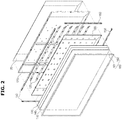
- FIG. 2 is an exploded perspective view showing a display module and a rear case of the display apparatus according to an exemplary embodiment
- FIG. 3 is an exploded perspective view showing a configuration of a part of the display module according to an exemplary embodiment.
- a display apparatus 1 may include, as shown in FIGS. 1 and 2 , a display module 100 configured to display images, a front case 10 and a rear case 20 which are coupled with each other in a front and back direction and which the display module 100 is disposed in between, and a control board disposed between the display module 100 and the rear case 20, and configured to transfer a supply voltage and signals to the display module 100.
- the display module 100 may include, as shown in FIGS. 2 and 3 , a display panel 110 formed as an LCD panel to display a screen, a backlight unit 120 disposed behind the display panel 110 to be spaced from the display panel 110, and configured to supply light to the display panel 110, a diffusion plate 130 disposed behind the display panel 110, and configured to diffuse light radiated from the backlight unit 120 to transfer the diffused light to the display panel 110, and various kinds of optical sheets 140 disposed in front of the diffusion plate 130.
- a display panel 110 formed as an LCD panel to display a screen
- a backlight unit 120 disposed behind the display panel 110 to be spaced from the display panel 110, and configured to supply light to the display panel 110
- a diffusion plate 130 disposed behind the display panel 110, and configured to diffuse light radiated from the backlight unit 120 to transfer the diffused light to the display panel 110
- various kinds of optical sheets 140 disposed in front of the diffusion plate 130.
- the display module 100 may include a middle mold 150 configured to support the display panel 110 and the diffusion plate 130, a top chassis 160 disposed in front of the middle mold 150 such that the display panel 110 is maintained to be installed in the middle mold 150, and a bottom chassis 170 disposed behind the middle mold 150, the bottom chassis 170 in which the backlight unit 120 is disposed.
- the backlight unit 120 may include a plurality of printed circuit boards (PCBs) 121 on each of which a conductive pattern is formed and which are disposed on the bottom chassis 170, a plurality of light sources 122 arranged on the front surfaces of the PCBs 121 to face the diffusion plate 130, and a plurality of circular lenses 123 installed on the light sources 122 to diffuse light generated from the light sources 122 (see FIG. 6 ).
- PCBs printed circuit boards
- the light sources 122 may be light-emitting diodes (LEDs).
- LEDs light-emitting diodes
- the light sources 122 are not limited to LEDs, and may be any other devices capable of irradiating light.
- the PCBs 121 may extend in the width direction of the display panel 110 in correspondence to the display panel 110, and the PCBs 121 may be arranged with intervals in parallel.
- a plurality of light sources 122 and a plurality of lenses 123 installed on the individual light sources 122 may be arranged with intervals in the length direction of the PCB 121, wherein the PCBs 121 may be connected to each other through a connection board.
- Each optical sheet 140 may include a prism film to focus light diffused by the diffusion plate 130 in a direction that is vertical to the display panel 110. Also, a protective film for protecting the optical sheet 140 may be additionally provided to contact the optical sheet 140.
- the middle mold 150 may support components, such as the display panel 110 and the diffusion plate 130, wherein the display panel 110 may be disposed in the front part of the middle mold 150 and the diffusion plate 130 may be disposed in the back part of the middle mold 150 (see FIG. 6 ).
- the middle mold 150 may be assembled at the lateral sides of the display module 100 in such a way to be removably coupled with the display module 100.
- the middle mold 150 may be integrated into the display module 100 in the shape of a frame.
- the top chassis 160 may include a bezel part 161 to cover the edges of the front part of the display panel 110, and a side part 162 bent from the outer borders of the bezel part 161 toward the back part of the display module 100.
- the bottom chassis 170 may include a flat part 171 having a nearly rectangular shape and provided in the shape of a flat plate in the center portion of the bottom chassis 170 such that a part of the backlight unit 120 rests on the flat part 171, and an inclined part 172 extending outward from the borders of the flat part 171 and inclined toward the front part of the display module 100.
- a plurality of resting grooves may be concavely formed through which the PCBs 121 of the backlight unit 120 can be rested on the bottom chassis 170.
- the display module 100 may include a first reflective sheet 180 disposed on the inner surface of the bottom chassis 170, and configured to reflect light radiated toward the inner surface of the bottom chassis 170 toward the display panel 110.
- the first reflective sheet 180 may include a sheet flat part 181 disposed on the inner surface of the flat part 171 of the bottom chassis 170, and a sheet inclined part 182 extending outward from the borders of the sheet flat part 181 and inclined with respect to the sheet flat part 181 in the front direction.
- a plurality of through holes 183 may be respectively formed to correspond to the plurality of light sources 122 and the plurality of lenses 123 so that the plurality of light sources 122 and the plurality of lenses 123 pass through the through holes 183 to protrude toward the inside of the first reflective sheet 180. Accordingly, light generated by the light sources 122 may be transferred to the display panel 110 disposed in the front direction, and light reflected backward by the diffusion plate 130 and a second reflective sheet 190 which will be described later may be again reflected in the front direction by the first reflective sheet 180.
- the sheet inclined part 182 may extend forward from the borders of the sheet flat part 181, that is, from the upper, lower, left, and right edges of the sheet flat part 181, and be inclined to face the rear surface of the display panel 110 so as to reflect light transferred from the light sources 122 in the front direction.
- the sheet inclined part 182 since the diffusion plate 130 is positioned behind the display panel 110, the sheet inclined part 182 may be inclined to face the rear surface of the diffusion plate 130.
- the peripheral portions of the display panel 110 may receive a relatively small amount of light as compared to a central portion, so that a shadow area that is darker than the central portion may appear at the peripheral portions of the display panel 110.
- the light sources 122 are additionally arranged on the inclined part 172. This will be described later.
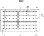
- FIG. 4 is a front view showing a configuration of a part of the display module 100 according to an exemplary embodiment
- FIG. 5 is a front view showing the rear part of the configuration of the part of the display module 100 according to an exemplary embodiment
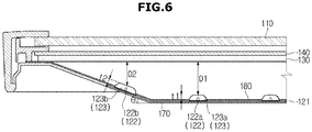
- FIG. 6 is an enlarged cross-sectional view showing the configuration of the part of the display module 100 according to an exemplary embodiment.
- the PCBs 121 may be supported on the inner surface of the bottom chassis 170. More specifically, the PCBs 121 may extend on the flat part 171 and the inclined part 172 in the inner surface of the bottom chassis 170, in such a way to be rested on the resting grooves formed concavely in the bottom chassis 170.
- the inclined part 172 may be inclined at an angle ⁇ of about 10 degrees with respect to the flat part 171.
- the inclined part 172 may be inclined at an angle of 8 to 15 degrees with respect to the flat part 171.
- the angle of the inclined part 172 in consideration of slimming the display apparatus 1.
- the inclined part of the bottom chassis is inclined at an angle of about 25 degrees.
- the angle ⁇ of the inclined part 172 by reducing the angle ⁇ of the inclined part 172 by about 10 degrees or more through an arrangement of the backlight unit 120 which will be described later, the display apparatus 1 can be slimmed.
- the PCBs 121 may include a first section 121a corresponding to the flat part 171, and a second section 121b extending from both side borders of the first section 121a and inclined at the same angle as that of the inclined part 172 to correspond to the inclined part 172.
- the first section 121a and the second section 121b may be coupled with the flat part 171 and the inclined part 172 to contact the flat part 171 and the inclined part 172, respectively. This is aimed at dissipating heat generated from the light sources 122 to the bottom chassis 170 through the PCBs 121.
- the bottom chassis 170 may be made of a metal material, such as aluminum or stainless steel, having a high heat transfer rate, to quickly diffuse heat generated from the light sources 122 along the surface to thereby help heat dissipation.
- At least one light source 122 (also, referred to as a second light source 122b) is arranged. Also, a plurality of light sources 122b may be arranged with intervals along the width direction of the second section 121b.
- some of the light sources 122 may be positioned on the inclined part 172. That is, some of the light sources 122 may be arranged at an inclination of a predetermined angle with respect to the light sources 122 (also, referred to as first light sources 122a) arranged on the flat part 171.
- Light emitted from the light sources 122 may be irradiated to the diffusion plate 130.
- the diffusion plate 130 may diffuse light passing therethrough, and transfer the diffused light to the display panel 110. If an amount of light is non-uniformly irradiated onto the entire area of the diffusion plate 130, non-uniform brightness distribution may appear on the display panel 110 so that some area of the display panel 110 shows different brightness.
- the light sources 122b arranged in the second section 121b are arranged with an inclination toward the diffusion plate 130 with respect to the light sources 122a arranged in the first section 121a, as described above, the light sources 122b may be positioned closer to the diffusion plate 130 than the light sources 122a.
- the light sources 122b arranged in the second section 121b and the light sources 122a arranged in the first section 121a may be located at different distances from the diffusion plate 130. Hence, differences in optical distance from the light sources 122 to the diffusion plate 130 may be made so as not to be able to uniformly irradiate light over the entire area of the diffusion plate 130.
- a range onto which light irradiated in a diagonal direction is transferred may be reduced by the shortened irradiation distance D so that a total area onto which light is transferred is reduced.
- an irradiation distance D of the first light sources 122a is referred to as a first distance D1 and an irradiation distance D of the second light sources 122b is referred to as a second distance D2
- the second distance D2 may be shorter than the first distance D1 since the second light sources 122b are located relatively closer to the diffusion plate 130 than the first light sources 122a.
- an area onto which light generated by the second light sources 122b is irradiated may be smaller than an area onto which light generated by the first light sources 122a is irradiated, so that the border portions of the diffusion plate 130 onto which light generated by the second light sources 122b is irradiated cannot receive an appropriate amount of light from the second light sources 122b.
- each second lens 123b may be greater than the diameter of each first lens 123a. As the diameter of a lens is greater, an amount of refraction of light may increase so that the light can be radiated to a wider area. (see FIG 6 )
- the thickness t2 of the second lens 123b may be thicker than the thickness t1 of the first lens 123a. As the thickness of a lens is thicker, an amount of refraction of light may increase accordingly.
- the distance D2 from the inclined part 172 to the diffusion plate 130 is shorter than the distance D1 from the flat part 161 to the diffusion plate 130, and a smaller number of light sources 122 are arranged in the inclined part 172 than in the flat part 171, light generated by the light sources 122 on the inclined part 171 can be radiated onto a wider area so as to radiate a sufficient amount of light onto the border portions of the diffusion plate 130, resulting in an increase in brightness of the border portions of the display panel 110.
- FIG. 7 is an exploded perspective view showing a configuration of a part of a display module according to another exemplary embodiment
- FIG. 8 is a front view showing the configuration of the part of the display module according to another exemplary embodiment
- FIG. 9 is an enlarged cross-sectional view showing the configuration of the part of the display module according to another exemplary embodiment.
- the backlight unit 200 may be supported inside the bottom chassis 170 by the flat part 171 and the inclined part 172.
- a first backlight unit 210 may be disposed in the flat part 171, and a second backlight unit 220 may be additionally disposed in the inclined part 172.
- the first backlight unit 210 may extend in the width (horizontal) direction of the display panel 110 in correspondence to the display panel 110. Also, a plurality of first backlight units 210 may be arranged at intervals in parallel. Each first backlight unit 210 may include a first PCB 211 extending in its length direction, a plurality of flat part light sources 212 arranged on the first PCB 211, and a plurality of flat part lenses 213 installed on the individual flat part light sources 212. The plurality of flat part light sources 212 and the plurality of flat part lenses 213 may be arranged with intervals in the length direction of the first backlight unit 210, and the plurality of first PCBs 211 may be connected to each other through a connection board.
- the second backlight unit 220 may extend in the height (vertical) direction of the display panel 220. Accordingly, the second backlight unit 220 may be perpendicular to the fist backlight unit 210. However, the second backlight unit 220 may be disposed at an arbitrary angle with respect to the first backlight unit 210, instead of being perpendicular to the first backlight unit 210.
- the second backlight unit 220 may be disposed on each of a pair of inclined parts 172 extending from both side borders of the flat part 171. However, a plurality of second backlight units 220 may be arranged with intervals in parallel in the width direction of the display panel 110.
- the second backlight unit 220 may include a second PCB 221 extending in its length direction, a plurality of inclined part light sources 222 arranged on the second PCB 221, and a plurality of inclined part lenses 223 installed on the individual inclined part light sources 222.
- the plurality of inclined part light sources 222 and the plurality of inclined part lenses 223 may be arranged with intervals in the length direction of the second PCB 221, and the plurality of second PCBs 221 may be, like the first PCBs 211, connected to each other through a connection board.
- the first PCB 211 and the second PCB 212 by applying different current to the first PCB 211 and the second PCB 212 to differentiate generation conditions of light of the light sources 212 and the light sources 222 respectively arranged on the first PCB 211 and the second PCB 212, it is possible to uniformly adjust light that is radiated onto the diffusion plate 130.
- the lenses provided in the flat part 171 and the lenses provided in the inclined part 172 are configured to have the same size, light that is radiated onto the diffusion plate 130 can be adjusted so as to achieve uniform brightness distribution on the display panel 110.
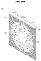
- FIG. 10A is a perspective view showing a front part of a second reflective sheet according to another exemplary embodiment
- FIG. 10B is a perspective view showing a front part of a second reflective sheet according to another exemplary embodiment
- FIG. 11 is an exploded perspective view showing a display module of a display apparatus according to another exemplary embodiment
- FIG. 12 is an exploded perspective view showing a configuration of a part of the display module according to another exemplary embodiment
- FIG. 13 is a cross-sectional view showing the configuration of the part of the display module according to another exemplary embodiment.
- a second reflective sheet 190 shown in FIG. 10A may be disposed in a inclined part 172 located in the left portion of a display module 300, and a second reflective sheet 190 located in the right portion of the display module 300 may be symmetrical to the second reflective sheet 190 of FIG. 10A .
- the inclined part light sources 222 may be provided in the inclined part 172, as described above.
- the plurality of light sources 122 arranged on the flat part 171 are located adjacent to each other, light radiated from the adjacent light sources 122 may overlap so that a nearly uniform amount of light can be radiated onto the center portion of the display panel 110 corresponding to the flat part 171.
- the display module 300 may further include the second reflective sheet 190.
- the second reflective sheet 190 may be provided between the display panel 110 and the first reflective sheet 180. More specifically, the second reflective sheet 190 may be disposed on a light path between the diffusion plate 130 and the inclined part light sources 222.
- the number of the second reflective sheets 190 may correspond to the number of the inclined part light sources 220.
- a reflective surface 191 may be formed with a material capable of effectively reflecting light.
- the second reflective sheet 190 may again reflect light radiated from the inclined part light sources 222 and proceeding toward the diffusion plate 130, and light reflected from the first reflective sheet 180, so as to direct the reflected light toward the first reflective sheet 180.
- a part of light radiated from the flat part light sources 212 may be irradiated onto the second reflective sheet 190.
- the light reflected and then irradiated onto the first reflective sheet 180 may be again reflected by the first reflective sheet 180, transmitted through the second reflective sheet 190 toward the diffusion plate 130, and then irradiated onto the diffusion plate 130.
- Light may be reflected by the first reflective sheet 180 and the second reflective sheet 190 one time and then irradiated onto the diffusion plate 130. Also, light may be repeatedly reflected by the first reflective sheet 180 and the second reflective sheet 190 several times, transmitted through the second reflective sheet 190, and then irradiated onto the diffusion plate 130.
- the second reflective sheet 190 may include a plurality of through holes 192 through which light is transmitted and irradiated onto the diffusion plate 130. A part of light radiated to the second reflective sheet 190 may be reflected from the reflective surface 191 toward the first reflective sheet 180, and the other part of the light may be irradiated onto the diffusion plate 130 through the through holes 192.
- the through holes 192 may be divided into a center part 191a located in the center portion of the reflective surface 191 of the second reflective sheet 190, and an edge part 191b extending outward from the center part 191a.
- the center part 191a may correspond to the location of the inclined part light source 222
- the edge part 191b may correspond to the outside of the circumference of the inclined part light source 222.
- center part 191a and the edge part 191b may be, instead of being definitely divided based on the radius of the circumference of the inclined part light source 222, determined in consideration of the size and thickness of the display module 300.
- a hot spot appearing as a brighter area than the other area may be made on an area on the display panel 110 corresponding to the center of the inclined part light source 222.
- no through holes 192 may be formed in the center portion of the center part 191a corresponding to the center portion of the inclined part light source 222. Therefore, a large amount of light radiated from the inclined part light source 222 may be not directly radiated to the diffusion plate 130.
- the through holes 192 may be gradually arranged toward the borders of the second reflective sheet 190, starting from a location spaced by a predetermined distance from the center of the center part 191a.
- a large amount of light may be radiated from the center of the inclined part light source 222 corresponding to the center part 191a, while a relatively small amount of light may be radiated from the edge portion of the inclined part light source 190 corresponding to the edge part 191b. Accordingly, in the edge part 191b, a larger amount of light may need to be radiated toward the diffusion plate 130 than in the center part 191a, with respect to an amount of light generated by the inclined part light source 222, in order to uniformly radiate light over the entire area of the diffusion plate 130 corresponding to the inclined part light source 222.
- the through holes 192 located closer to the center of the center part 191a may have the smaller diameters, and the through holes 192 located closer to the outermost area of the edge part 191b may have the larger diameters. Also, the number of the through holes 192 arranged in the edge part 191b may be greater than that of the through holes 192 arranged in the center part 191a.
- the through holes 192 having the smaller diameters may be arranged in the center part 191a to reduce an amount of light to be transmitted with respect to a total amount of radiated light by a predetermined amount, and the through holes 192 having the greater diameters may be arranged in the edge part 191b to which a small amount of light is radiated to transmit a relatively large amount of light with respect to the total amount of radiated light.
- the through holes 192 may be arranged in various patterns according to the size and thickness of the display module 300.
- the second reflective sheet 190 may be disposed between the display panel 110 and the inclined part light source 222, as described above. Accordingly, the second reflective sheet 190 may include a contact part 195 extending from its one side edge such that the second reflective sheet 190 is supported on the inclined part 172 at the side edge.
- the contact part 195 may contact one side edge of the inclined part 172 when the display module 300 is assembled.
- a contact groove may be formed to correspond to the contact part 195, at an area at which the inclined part 172 contacts the contact part 195, so that the second reflective sheet 190 can be rested on the inclined part 172.
- the contact part 195 may be coupled with the inclined part 172 by an adhesive such as glue.
- the second reflective sheet 190 may include an additional coupling unit to be coupled with the inclined part 172 by screw coupling.
- a contact bar 196 may extend vertically toward the flat part 171. Since no component for supporting the second reflective sheet 190 laterally exists at the other side edge of the second reflective sheet 190, the contact bar 196 may be used to support the second reflective sheet 190 on the flat part 171 located below the other side edge of the second reflective sheet 190.
- the contact bar 196 may extend vertically from the rear part of the second reflective sheet 190 to contact the surface of the flat part 171. At a location of the flat part 171 corresponding to the contact bar 196, a contact groove may be formed to rest the contact bar 196 therein.
- the contact bar 196 may be attached on the flat part 171 by an adhesive such as glue.
- the second reflective sheet 190 may include an additional coupling unit to be coupled with the flat part 171 by screw coupling.
- FIG. 10B shows a second reflective sheet 190 according to another exemplary embodiment.
- a bent part 197 bent vertically and extending from the other side edge of the second reflective sheet 190, instead of the contact bar 196, may be provided.
- the bent part 197 may extend vertically toward the flat part 171, like the contact bar 196, and the side end 197a of the bent part 197 may contact the surface of the flat part 171.
- a contact groove may be formed to correspond to the side end 197a of the bent part 197, at an area at which the side end 197a of the bent part 197 contacts the flat part 171, so that the second reflective sheet 190 can be rested on the flat part 171.
- a plurality of through holes 192 may be, unlike the current embodiment, formed so that light radiated from the inclined part light source 222 can be transmitted toward the flat part 171 or light radiated from the flat part light source 212 can be transmitted to the inclined part 172.
- the through holes 192 of the bent part 197 may be formed with various sizes and shapes.
- the contact bar 196 or the bent part 197 may extend upward and downward, instead of extending backward, so that the second reflective sheet 190 can be supported by the middle mold 150 or by the upper and lower side edges of the bottom chassis 170.
- FIG. 14A is a view for describing a concept in which light radiated from a light source according to another exemplary embodiment is emitted toward the reflective surface 191 of the second reflective sheet 190
- FIG. 14B is a view for describing a concept in which light is transmitted through the second reflective sheet 190 according to another exemplary embodiment
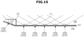
- FIG. 15 is a view for describing a concept in which light is radiated from a plurality of light sources according to another exemplary embodiment.
- a large amount of light L1 generated from the center of the inclined part light source 222 may be irradiated onto the center part 191a of the second reflective sheet 190.
- the light L1 since no through holes 192 are formed in the center portion of the center part 191a, the light L1 may be not radiated toward the diffusion plate 130.
- the number of the through holes 192 may increase, and the diameters of the through holes 192 may also increase. That is, the diameters of the through holes 192 may increase in the order of 192c > 192b > 192a.
- an amount of light L5 transmitted through the through hole 192c formed in the edge part 191b may be more than an amount of light L3 transmitted through the through hole 192a formed around the center part 191a.
- an amount of light radiated toward the center part 191a may be more than an amount of light radiated toward the edge part 191b so that a total amount of light transmitted through the second reflective sheet 190 can be uniformly maintained throughout the center part 191a and the edge part 191b.
- the light L1 and L2 not transmitted through the through holes 192 may be reflected by the reflective surface 191 and radiated toward the inclined part light source 222. Then, the light L1 and L2 may be reflected by the first reflective sheet 180, and again directed toward the second reflective sheet 190.
- a part of light transmitted through the second reflective sheet 190 by single or multiple reflections may be radiated toward an area of the display panel 110 corresponding to the center part 191a according to an angle of reflection of the light, so that a constant amount of light can be radiated toward the display panel 110.
- some light L6 generated from the flat part light source 212 may be emitted toward the second reflective sheet 190 and transmitted through the through hole 192 so as to be radiated toward the area of the display panel 110 corresponding to the center part 191a.
- FIG. 15 schematically shows light radiated from the flat part light source 212 and the inclined part light source 222.
- Light Lc radiated from the flat part light source 212 may overlap with light radiated from the adjacent light sources 212 so that a nearly constant amount of light can be radiated toward the area of the display panel 110 corresponding to the flat part 171.
- the inclined part light source 222 is inclined with respect to the display panel 110, as described above, light generated from the inclined part light source 222 may be intensively radiated onto a specific location. Also, since the number of light sources arranged adjacent to each other is small, a constant amount of light La cannot be radiated toward the area of the display panel 110 corresponding to the inclined surface 172.
- the second reflective sheet 190 may be disposed between the inclined part light source 222 and the display panel 110.
- FIG. 16 is a perspective view of a second reflective sheet according to another exemplary embodiment
- FIG. 17 is an exploded perspective view showing a configuration of a part of a display module according to an exemplary embodiment
- FIG. 18 is an enlarged perspective view showing the configuration of the part of the display module according to another exemplary embodiment.
- a second reflective sheet 290 shown in FIG. 16 may be provided to correspond to the inclined part 172 located in the right portion of the display module 300, and a second reflective sheet 290 provided to correspond to the inclined part 172 located in the left portion of the display module 300 may be symmetrical to the second reflective sheet 290 shown in FIG 16 .
- the second reflective sheet 290 may be formed with a plate of a size corresponding to the vertical length of the inclined part 172. Unlike the second reflective sheet 190 according to the above-described embodiment, the second reflective sheet 290 according to another exemplary embodiment may be provided in each of the pair of inclined parts 172 provided in both side edges of the display module 300.
- the second reflective sheet 290 may include a plurality of center parts 291a respectively positioned at locations corresponding to the plurality of inclined part light sources 222, and a plurality of edge parts 291b extending outward from the circumferences of the center parts 291a.
- Each center part 291a and each edge part 291b may respectively have the same technical features as the center part 191a and the edge part 191b of the above-described embodiment, and accordingly, a detailed description thereof will be omitted.
- a resting part 295 extending outward from the second reflective sheet 290 may be respectively provided to rest the second reflective sheet 290 on the inclined part 172. More specifically, one side border and upper and lower borders of the second reflective sheet 290, adjacent to the inclined part 172, may be formed as a resting part 295 so as to pass through the first reflective sheet 180 and to be rested on the bottom chassis 170 and supported by the bottom chassis 170.
- the first reflective sheet 180 may include a resting hole 185 through which the resting part 295 can pass and which has a size corresponding to the resting part 295.
- a resting groove 175 may be formed with a size corresponding to the size of the resting part 295, at a location corresponding to the resting part 295 passed through the resting hole 185, so that the resting part 295 can be partially inserted into the bottom chassis 170 and rested on the bottom chassis 170.
- the second reflective sheet 290 may be rested on the bottom chassis 170 to be disposed between the inclined part light sources 222 and the display panel 110, so that an uniform amount of light can be radiated to the area of the display panel 110 corresponding to the inclined part light sources 222.
- the display apparatus for example, a slim display apparatus
- the backlight unit in the inclined part formed in the rear part of the display apparatus, it is possible to effectively transmit light to the entire area of the display panel, resulting in an improvement in efficiency of the display apparatus.
Landscapes
- Physics & Mathematics (AREA)
- Nonlinear Science (AREA)
- Mathematical Physics (AREA)
- Chemical & Material Sciences (AREA)
- Crystallography & Structural Chemistry (AREA)
- General Physics & Mathematics (AREA)
- Optics & Photonics (AREA)
- Engineering & Computer Science (AREA)
- General Engineering & Computer Science (AREA)
- Microelectronics & Electronic Packaging (AREA)
- Planar Illumination Modules (AREA)
- Liquid Crystal (AREA)
Description
- Apparatuses consistent with exemplary embodiments relate to a display apparatus, and more particularly, to structure of a backlight unit of irradiating light.
- In general, a display module of a display apparatus, such as a monitor and a television, includes a display panel to display images.
- A liquid crystal display (LCD) panel is widely used as such a display panel. However, since an LCD panel cannot itself emit light, a backlight unit is disposed behind the display panel, and a diffusion plate is disposed between the display panel and the backlight unit to diffuse light radiated from the backlight unit so as to uniformly distribute the light to the entire area of the display panel.
- The display module may also include a reflective sheet disposed inside a bottom chassis forming a rear side of the display module to again reflect light reflected toward the bottom chassis toward the display panel.
- In order to transmit light generated from the backlight unit and the reflective sheet to the entire area of the display panel, a predetermined optical distance is required.
- However, as display apparatuses become slimmer, the optical distance between the backlight unit and the display panel is reduced, which causes a problem that light cannot be uniformly radiated to the entire area of the display panel.
-
EP 2 811 336 A2 shows an illuminating apparatus and LCD having the same and discloses the features of the preamble ofclaim 1. - According to the present invention, there is provided a display apparatus as set forth in the appended claims. The display apparatus including: a display panel; a chassis including a flat part and an inclined part that extends from a side border of the flat part and is inclined with respect to the flat part; at least one printed circuit board (PCB) disposed on the chassis; and a plurality of light sources arranged on the at least one PCB and configured to emit light toward the display panel, wherein at least one light source of the plurality of light sources is arranged on the inclined part of the chassis the display apparatus comprises a plurality of lenses respectively installed on the plurality of light sources wherein a size of at least one lens among the plurality of lenses installed on the at least one light source arranged on the inclined part is greater than the size of other lenses among the plurality of lenses installed on other light sources of the plurality of light sources arranged on a portion of the at least one PCB which is displayed on the flat part other features. Other features of the invention will be apparent from the dependent claims and the description which follows.
- The above and/or other aspects will become apparent and more readily appreciated from the following description of exemplary embodiments, taken in conjunction with the accompanying drawings of which:
-
FIG. 1 is a perspective view of a display apparatus according to an exemplary embodiment; -
FIG. 2 is an exploded perspective view showing a display module and a rear case of a display apparatus according to an exemplary embodiment; -
FIG. 3 is an exploded perspective view showing a configuration of a part of a display module according to an exemplary embodiment; -
FIG. 4 is a front view showing a configuration of a part of a display module according to an exemplary embodiment; -
FIG. 5 is a perspective view showing a rear part of a configuration of a part of a display module according to an exemplary embodiment; -
FIG. 6 is an enlarged cross-sectional view showing a configuration of a part of a display module according to an exemplary embodiment; -
FIG. 7 is an exploded perspective view showing a configuration of a part of a display module according to another exemplary embodiment; -
FIG. 8 is a front view showing a configuration of a part of a display module according to another exemplary embodiment; -
FIG. 9 is an enlarged cross-sectional view showing a configuration of a part of a display module according to another exemplary embodiment; -
FIG. 10A is a perspective view showing a front part of a second reflective sheet according to another exemplary embodiment; -
FIG. 10B is a perspective view showing a front part of a second reflective sheet according to another exemplary embodiment; -
FIG. 11 is an exploded perspective view showing a display module of a display apparatus according to another exemplary embodiment; -
FIG. 12 is an exploded perspective view showing a configuration of a part of a display module according to another exemplary embodiment; -
FIG. 13 is a cross-sectional view showing a configuration of a part of a display module according to another exemplary embodiment; -
FIG. 14A is a view for describing a concept in which light radiated from a light source according to another exemplary embodiment is emitted toward a reflective surface of a second reflective sheet; -
FIG. 14B is a view for describing a concept in which light is transmitted through a second reflective sheet according to another exemplary embodiment; -
FIG. 15 is a view for describing a concept in which light is radiated from a plurality of light sources according to another exemplary embodiment; -
FIG. 16 is a perspective view of a second reflective sheet according to another exemplary embodiment; -
FIG. 17 is an exploded perspective view showing a configuration of a part of a display module according to another exemplary embodiment; and -
FIG. 18 is an enlarged perspective view showing a configuration of a part of a display module according to another exemplary embodiment. - Configurations illustrated in the embodiments and the drawings described in the present specification are merely exemplary, and thus it is to be understood that various modified examples, which may replace the embodiments and the drawings described in the present specification, are possible.
- Also, like reference numerals or symbols denoted in the drawings of the present specification represent members or components that perform the substantially same functions.
- The terms used in the present specification are used to describe the exemplary embodiments. Accordingly, it should be apparent to those skilled in the art that the following description of exemplary embodiments is provided for illustration purpose only and not for the purpose of limiting the inventive concept as defined by the appended claims and their equivalents. It is to be understood that the singular forms "a," "an," and "the" include plural referents unless the context clearly dictates otherwise. It will be understood that when the terms "includes," "comprises," "including," and/or "comprising," when used in this specification, specify the presence of stated features, figures, steps, components, or combination thereof, but do not preclude the presence or addition of one or more other features, figures, steps, components, members, or combinations thereof.
- Hereinafter, exemplary embodiments will be described in detail with reference to the accompanying drawings.
- In the following description, the terms "front part" and "front direction" mean the front part of a display apparatus shown in
FIG. 1 and a direction toward the front part of the display apparatus, respectively, and also, the term "rear direction" means a direction toward the rear part of thedisplay apparatus 1. - The following description will be given under an assumption that the
display apparatus 1 is a flat panel display apparatus, however, thedisplay apparatus 1 may be a curved display apparatus or a bendable or flexible display apparatus that can change its state between a flat state and a curved state. - Also, the present disclosure can be applied to all kinds of display apparatuses regardless of their screen sizes. For example, the present disclosure can be applied to a product, such as a smart television, a monitor, and the like, which can be put on a table, a wall, a ceiling, etc., or to a portable product, such as a tablet Personal Computer (PC), a laptop computer, a smart phone, e-book, and the like.
-
FIG. 1 is a perspective view of a display apparatus according to an exemplary embodiment,FIG. 2 is an exploded perspective view showing a display module and a rear case of the display apparatus according to an exemplary embodiment, andFIG. 3 is an exploded perspective view showing a configuration of a part of the display module according to an exemplary embodiment. - A
display apparatus 1 may include, as shown inFIGS. 1 and2 , adisplay module 100 configured to display images, afront case 10 and arear case 20 which are coupled with each other in a front and back direction and which thedisplay module 100 is disposed in between, and a control board disposed between thedisplay module 100 and therear case 20, and configured to transfer a supply voltage and signals to thedisplay module 100. - The
display module 100 may include, as shown inFIGS. 2 and3 , adisplay panel 110 formed as an LCD panel to display a screen, abacklight unit 120 disposed behind thedisplay panel 110 to be spaced from thedisplay panel 110, and configured to supply light to thedisplay panel 110, adiffusion plate 130 disposed behind thedisplay panel 110, and configured to diffuse light radiated from thebacklight unit 120 to transfer the diffused light to thedisplay panel 110, and various kinds ofoptical sheets 140 disposed in front of thediffusion plate 130. - Further, the
display module 100 may include amiddle mold 150 configured to support thedisplay panel 110 and thediffusion plate 130, atop chassis 160 disposed in front of themiddle mold 150 such that thedisplay panel 110 is maintained to be installed in themiddle mold 150, and abottom chassis 170 disposed behind themiddle mold 150, thebottom chassis 170 in which thebacklight unit 120 is disposed. - The
backlight unit 120 may include a plurality of printed circuit boards (PCBs) 121 on each of which a conductive pattern is formed and which are disposed on thebottom chassis 170, a plurality oflight sources 122 arranged on the front surfaces of thePCBs 121 to face thediffusion plate 130, and a plurality ofcircular lenses 123 installed on thelight sources 122 to diffuse light generated from the light sources 122 (seeFIG. 6 ). - According to an exemplary embodiment, the
light sources 122 may be light-emitting diodes (LEDs). However, thelight sources 122 are not limited to LEDs, and may be any other devices capable of irradiating light. - In the current embodiment, the
PCBs 121 may extend in the width direction of thedisplay panel 110 in correspondence to thedisplay panel 110, and thePCBs 121 may be arranged with intervals in parallel. On eachPCB 121, a plurality oflight sources 122 and a plurality oflenses 123 installed on theindividual light sources 122 may be arranged with intervals in the length direction of thePCB 121, wherein thePCBs 121 may be connected to each other through a connection board. - Each
optical sheet 140 may include a prism film to focus light diffused by thediffusion plate 130 in a direction that is vertical to thedisplay panel 110. Also, a protective film for protecting theoptical sheet 140 may be additionally provided to contact theoptical sheet 140. - The
middle mold 150 may support components, such as thedisplay panel 110 and thediffusion plate 130, wherein thedisplay panel 110 may be disposed in the front part of themiddle mold 150 and thediffusion plate 130 may be disposed in the back part of the middle mold 150 (seeFIG. 6 ). - According to an exemplary embodiment, the
middle mold 150 may be assembled at the lateral sides of thedisplay module 100 in such a way to be removably coupled with thedisplay module 100. However, themiddle mold 150 may be integrated into thedisplay module 100 in the shape of a frame. Thetop chassis 160 may include abezel part 161 to cover the edges of the front part of thedisplay panel 110, and aside part 162 bent from the outer borders of thebezel part 161 toward the back part of thedisplay module 100. - The
bottom chassis 170 may include aflat part 171 having a nearly rectangular shape and provided in the shape of a flat plate in the center portion of thebottom chassis 170 such that a part of thebacklight unit 120 rests on theflat part 171, and aninclined part 172 extending outward from the borders of theflat part 171 and inclined toward the front part of thedisplay module 100. In theflat part 171 and theinclined part 172, a plurality of resting grooves may be concavely formed through which thePCBs 121 of thebacklight unit 120 can be rested on thebottom chassis 170. - Also, the
display module 100 may include a firstreflective sheet 180 disposed on the inner surface of thebottom chassis 170, and configured to reflect light radiated toward the inner surface of thebottom chassis 170 toward thedisplay panel 110. - The first
reflective sheet 180 may include a sheetflat part 181 disposed on the inner surface of theflat part 171 of thebottom chassis 170, and a sheetinclined part 182 extending outward from the borders of the sheetflat part 181 and inclined with respect to the sheetflat part 181 in the front direction. - In the sheet
flat part 181, a plurality of throughholes 183 may be respectively formed to correspond to the plurality oflight sources 122 and the plurality oflenses 123 so that the plurality oflight sources 122 and the plurality oflenses 123 pass through the throughholes 183 to protrude toward the inside of the firstreflective sheet 180. Accordingly, light generated by thelight sources 122 may be transferred to thedisplay panel 110 disposed in the front direction, and light reflected backward by thediffusion plate 130 and a secondreflective sheet 190 which will be described later may be again reflected in the front direction by the firstreflective sheet 180. - The sheet inclined
part 182 may extend forward from the borders of the sheetflat part 181, that is, from the upper, lower, left, and right edges of the sheetflat part 181, and be inclined to face the rear surface of thedisplay panel 110 so as to reflect light transferred from thelight sources 122 in the front direction. In the current embodiment, since thediffusion plate 130 is positioned behind thedisplay panel 110, the sheet inclinedpart 182 may be inclined to face the rear surface of thediffusion plate 130. - In the
display module 100, if thelight sources 122 are arranged only on theflat part 171, the peripheral portions of thedisplay panel 110 may receive a relatively small amount of light as compared to a central portion, so that a shadow area that is darker than the central portion may appear at the peripheral portions of thedisplay panel 110. In order to prevent such a shadow area, thelight sources 122 are additionally arranged on theinclined part 172. This will be described later. -
FIG. 4 is a front view showing a configuration of a part of thedisplay module 100 according to an exemplary embodiment,FIG. 5 is a front view showing the rear part of the configuration of the part of thedisplay module 100 according to an exemplary embodiment, andFIG. 6 is an enlarged cross-sectional view showing the configuration of the part of thedisplay module 100 according to an exemplary embodiment. - As shown in
FIGS. 4 and5 , thePCBs 121 may be supported on the inner surface of thebottom chassis 170. More specifically, thePCBs 121 may extend on theflat part 171 and theinclined part 172 in the inner surface of thebottom chassis 170, in such a way to be rested on the resting grooves formed concavely in thebottom chassis 170. - The
inclined part 172 may be inclined at an angle θ of about 10 degrees with respect to theflat part 171. Theinclined part 172 may be inclined at an angle of 8 to 15 degrees with respect to theflat part 171. - The angle of the
inclined part 172 in consideration of slimming thedisplay apparatus 1. In a general direct type display apparatus, the inclined part of the bottom chassis is inclined at an angle of about 25 degrees. However, by reducing the angle θ of theinclined part 172 by about 10 degrees or more through an arrangement of thebacklight unit 120 which will be described later, thedisplay apparatus 1 can be slimmed. - The
PCBs 121 may include afirst section 121a corresponding to theflat part 171, and asecond section 121b extending from both side borders of thefirst section 121a and inclined at the same angle as that of theinclined part 172 to correspond to theinclined part 172. - The
first section 121a and thesecond section 121b may be coupled with theflat part 171 and theinclined part 172 to contact theflat part 171 and theinclined part 172, respectively. This is aimed at dissipating heat generated from thelight sources 122 to thebottom chassis 170 through thePCBs 121. - Accordingly, the
bottom chassis 170 may be made of a metal material, such as aluminum or stainless steel, having a high heat transfer rate, to quickly diffuse heat generated from thelight sources 122 along the surface to thereby help heat dissipation. - In the
second section 121b, at least one light source 122 (also, referred to as a secondlight source 122b) is arranged. Also, a plurality oflight sources 122b may be arranged with intervals along the width direction of thesecond section 121b. - Due to the
light sources 122b arranged on thesecond section 121b, some of thelight sources 122 may be positioned on theinclined part 172. That is, some of thelight sources 122 may be arranged at an inclination of a predetermined angle with respect to the light sources 122 (also, referred to asfirst light sources 122a) arranged on theflat part 171. - Light emitted from the
light sources 122 may be irradiated to thediffusion plate 130. Thediffusion plate 130 may diffuse light passing therethrough, and transfer the diffused light to thedisplay panel 110. If an amount of light is non-uniformly irradiated onto the entire area of thediffusion plate 130, non-uniform brightness distribution may appear on thedisplay panel 110 so that some area of thedisplay panel 110 shows different brightness. - Since the
light sources 122b arranged in thesecond section 121b are arranged with an inclination toward thediffusion plate 130 with respect to thelight sources 122a arranged in thefirst section 121a, as described above, thelight sources 122b may be positioned closer to thediffusion plate 130 than thelight sources 122a. - Accordingly, the
light sources 122b arranged in thesecond section 121b and thelight sources 122a arranged in thefirst section 121a may be located at different distances from thediffusion plate 130. Hence, differences in optical distance from thelight sources 122 to thediffusion plate 130 may be made so as not to be able to uniformly irradiate light over the entire area of thediffusion plate 130. - Particularly, as an irradiation distance D is shortened, a range onto which light irradiated in a diagonal direction is transferred may be reduced by the shortened irradiation distance D so that a total area onto which light is transferred is reduced.
- If an irradiation distance D of the
first light sources 122a is referred to as a first distance D1 and an irradiation distance D of the secondlight sources 122b is referred to as a second distance D2, the second distance D2 may be shorter than the first distance D1 since the secondlight sources 122b are located relatively closer to thediffusion plate 130 than thefirst light sources 122a. - Accordingly, an area onto which light generated by the second
light sources 122b is irradiated may be smaller than an area onto which light generated by thefirst light sources 122a is irradiated, so that the border portions of thediffusion plate 130 onto which light generated by the secondlight sources 122b is irradiated cannot receive an appropriate amount of light from the secondlight sources 122b. According to the invention and as shown inFIG. 4 by differentiating the sizes of the lenses 123 (also, referred to asfirst lenses 123a) installed on thefirst light sources 122a from the sizes of the lenses 123 (also, referred to assecond lenses 123b) installed on the secondlight sources 122b to irradiate light onto the outermost border portions of thediffusion plate 130, it is possible to achieve uniform brightness distribution on thedisplay panel 110. - That is, by expanding an angle of irradiation of light through the
second lenses 123b, it is possible to sufficiently irradiate light to the border portions of thediffusion plate 130. - More specifically, the diameter of each
second lens 123b may be greater than the diameter of eachfirst lens 123a. As the diameter of a lens is greater, an amount of refraction of light may increase so that the light can be radiated to a wider area. (seeFIG 6 ) - For the same reason, the thickness t2 of the
second lens 123b may be thicker than the thickness t1 of thefirst lens 123a. As the thickness of a lens is thicker, an amount of refraction of light may increase accordingly. - Accordingly, although the distance D2 from the
inclined part 172 to thediffusion plate 130 is shorter than the distance D1 from theflat part 161 to thediffusion plate 130, and a smaller number oflight sources 122 are arranged in theinclined part 172 than in theflat part 171, light generated by thelight sources 122 on theinclined part 171 can be radiated onto a wider area so as to radiate a sufficient amount of light onto the border portions of thediffusion plate 130, resulting in an increase in brightness of the border portions of thedisplay panel 110. - Hereinafter, a display apparatus according to another exemplary embodiment will be described. In the following description, descriptions about the same components as those of the above-described embodiment will be omitted.
-
FIG. 7 is an exploded perspective view showing a configuration of a part of a display module according to another exemplary embodiment,FIG. 8 is a front view showing the configuration of the part of the display module according to another exemplary embodiment, andFIG. 9 is an enlarged cross-sectional view showing the configuration of the part of the display module according to another exemplary embodiment. - As shown in
FIGS. 7 and8 , thebacklight unit 200 may be supported inside thebottom chassis 170 by theflat part 171 and theinclined part 172. - More specifically, a
first backlight unit 210 may be disposed in theflat part 171, and asecond backlight unit 220 may be additionally disposed in theinclined part 172. - The
first backlight unit 210 may extend in the width (horizontal) direction of thedisplay panel 110 in correspondence to thedisplay panel 110. Also, a plurality offirst backlight units 210 may be arranged at intervals in parallel. Eachfirst backlight unit 210 may include afirst PCB 211 extending in its length direction, a plurality of flat partlight sources 212 arranged on thefirst PCB 211, and a plurality offlat part lenses 213 installed on the individual flat partlight sources 212. The plurality of flat partlight sources 212 and the plurality offlat part lenses 213 may be arranged with intervals in the length direction of thefirst backlight unit 210, and the plurality offirst PCBs 211 may be connected to each other through a connection board. - The
second backlight unit 220 may extend in the height (vertical) direction of thedisplay panel 220. Accordingly, thesecond backlight unit 220 may be perpendicular to thefist backlight unit 210. However, thesecond backlight unit 220 may be disposed at an arbitrary angle with respect to thefirst backlight unit 210, instead of being perpendicular to thefirst backlight unit 210. - The
second backlight unit 220 may be disposed on each of a pair ofinclined parts 172 extending from both side borders of theflat part 171. However, a plurality ofsecond backlight units 220 may be arranged with intervals in parallel in the width direction of thedisplay panel 110. - The
second backlight unit 220 may include asecond PCB 221 extending in its length direction, a plurality of inclinedpart light sources 222 arranged on thesecond PCB 221, and a plurality ofinclined part lenses 223 installed on the individual inclinedpart light sources 222. The plurality of inclinedpart light sources 222 and the plurality ofinclined part lenses 223 may be arranged with intervals in the length direction of thesecond PCB 221, and the plurality ofsecond PCBs 221 may be, like thefirst PCBs 211, connected to each other through a connection board. - Also, according to the invention and like the above-described embodiment of differentiating the sizes of the
first lenses 123a from the sizes of thesecond lenses 123b, by differentiating the sizes of theinclined part lenses 223 from the sizes of theflat part lenses 213, it is possible to cancel differences in optical distance made between the inclinedpart light sources 222 and the flat partlight sources 212. - Also, by applying different current to the
first PCB 211 and thesecond PCB 212 to differentiate generation conditions of light of thelight sources 212 and thelight sources 222 respectively arranged on thefirst PCB 211 and thesecond PCB 212, it is possible to uniformly adjust light that is radiated onto thediffusion plate 130. - Although the lenses provided in the
flat part 171 and the lenses provided in theinclined part 172 are configured to have the same size, light that is radiated onto thediffusion plate 130 can be adjusted so as to achieve uniform brightness distribution on thedisplay panel 110. - Hereinafter, a display apparatus according to another exemplary embodiment will be described. In the following description, descriptions about the same components as those of the above-described embodiment will be omitted.
-
FIG. 10A is a perspective view showing a front part of a second reflective sheet according to another exemplary embodiment,FIG. 10B is a perspective view showing a front part of a second reflective sheet according to another exemplary embodiment,FIG. 11 is an exploded perspective view showing a display module of a display apparatus according to another exemplary embodiment,FIG. 12 is an exploded perspective view showing a configuration of a part of the display module according to another exemplary embodiment, andFIG. 13 is a cross-sectional view showing the configuration of the part of the display module according to another exemplary embodiment. - A second
reflective sheet 190 shown inFIG. 10A may be disposed in ainclined part 172 located in the left portion of adisplay module 300, and a secondreflective sheet 190 located in the right portion of thedisplay module 300 may be symmetrical to the secondreflective sheet 190 ofFIG. 10A . - In order to achieve uniform brightness distribution throughout the entire area of the
display panel 110, the inclined part light sources 222 (also, referred to as the second light sources 222b) may be provided in theinclined part 172, as described above. - Since light generated from the inclined
part light sources 222, unlike the flat part light sources 212 (also, referred to as the second light sources 212a) arranged on theflat part 171, is radiated at a predetermined angle with respect to thedisplay panel 110, the light cannot be uniformly radiated onto the border portions of thedisplay panel 110 corresponding to the inclinedpart light sources 222. - Also, since the plurality of
light sources 122 arranged on theflat part 171 are located adjacent to each other, light radiated from the adjacentlight sources 122 may overlap so that a nearly uniform amount of light can be radiated onto the center portion of thedisplay panel 110 corresponding to theflat part 171. - However, since a smaller number of
light sources 122 are arranged in theinclined part 172 than in theflat part 171, the effect of uniformizing light due to overlapping of light radiated from adjacent light sources cannot be obtained. Accordingly, light cannot be uniformly radiated onto the border portions of thedisplay panel 110 rather than the center portion of thedisplay panel 110. - In order to acquire an uniform amount of light in the border portions of the
display panel 110, thedisplay module 300 may further include the secondreflective sheet 190. - The second
reflective sheet 190 may be provided between thedisplay panel 110 and the firstreflective sheet 180. More specifically, the secondreflective sheet 190 may be disposed on a light path between thediffusion plate 130 and the inclinedpart light sources 222. - There may be provided a plurality of second
reflective sheets 190 to respectively correspond to the plurality of inclinedpart light sources 220 arranged on theinclined part 171. Accordingly, the number of the secondreflective sheets 190 may correspond to the number of the inclinedpart light sources 220. - On one surface of the second
reflective sheet 190 facing the firstreflective sheet 180, areflective surface 191 may be formed with a material capable of effectively reflecting light. - The second
reflective sheet 190 may again reflect light radiated from the inclinedpart light sources 222 and proceeding toward thediffusion plate 130, and light reflected from the firstreflective sheet 180, so as to direct the reflected light toward the firstreflective sheet 180. - Also, a part of light radiated from the flat part
light sources 212 may be irradiated onto the secondreflective sheet 190. - The light reflected and then irradiated onto the first
reflective sheet 180 may be again reflected by the firstreflective sheet 180, transmitted through the secondreflective sheet 190 toward thediffusion plate 130, and then irradiated onto thediffusion plate 130. - Light may be reflected by the first
reflective sheet 180 and the secondreflective sheet 190 one time and then irradiated onto thediffusion plate 130. Also, light may be repeatedly reflected by the firstreflective sheet 180 and the secondreflective sheet 190 several times, transmitted through the secondreflective sheet 190, and then irradiated onto thediffusion plate 130. - The second
reflective sheet 190 may include a plurality of throughholes 192 through which light is transmitted and irradiated onto thediffusion plate 130. A part of light radiated to the secondreflective sheet 190 may be reflected from thereflective surface 191 toward the firstreflective sheet 180, and the other part of the light may be irradiated onto thediffusion plate 130 through the throughholes 192. - The through
holes 192 may be divided into acenter part 191a located in the center portion of thereflective surface 191 of the secondreflective sheet 190, and anedge part 191b extending outward from thecenter part 191a. Thecenter part 191a may correspond to the location of the inclinedpart light source 222, and theedge part 191b may correspond to the outside of the circumference of the inclinedpart light source 222. - However, the
center part 191a and theedge part 191b may be, instead of being definitely divided based on the radius of the circumference of the inclinedpart light source 222, determined in consideration of the size and thickness of thedisplay module 300. - Since a majority of light is radiated from the center of the inclined
light source 222, a hot spot appearing as a brighter area than the other area may be made on an area on thedisplay panel 110 corresponding to the center of the inclinedpart light source 222. - The reason is because the amount of light is cancelled by the adjacent inclined
part light sources 222 so that an uniform amount of light cannot be radiated, unlike the flat partlight sources 212, as described above. - In order to overcome the problem, no through
holes 192 may be formed in the center portion of thecenter part 191a corresponding to the center portion of the inclinedpart light source 222. Therefore, a large amount of light radiated from the inclinedpart light source 222 may be not directly radiated to thediffusion plate 130. - Since light radiated from the inclined
part light source 222 is transmitted through the secondreflective sheet 190 and then radiated to thedisplay panel 110, a relatively smaller amount of light can be radiated to theedge portions 172 of thedisplay panel 110 than that radiated to the center portion of thedisplay panel 110 corresponding to theflat part 171. - Accordingly, by applying different amounts of electricity to the inclined
part light sources 222 and the flat partlight sources 212, respectively, it is possible to adjust an irradiation amount of light, as described above. - The through
holes 192 may be gradually arranged toward the borders of the secondreflective sheet 190, starting from a location spaced by a predetermined distance from the center of thecenter part 191a. - As described above, a large amount of light may be radiated from the center of the inclined
part light source 222 corresponding to thecenter part 191a, while a relatively small amount of light may be radiated from the edge portion of the inclinedpart light source 190 corresponding to theedge part 191b. Accordingly, in theedge part 191b, a larger amount of light may need to be radiated toward thediffusion plate 130 than in thecenter part 191a, with respect to an amount of light generated by the inclinedpart light source 222, in order to uniformly radiate light over the entire area of thediffusion plate 130 corresponding to the inclinedpart light source 222. - Accordingly, the through
holes 192 located closer to the center of thecenter part 191a may have the smaller diameters, and the throughholes 192 located closer to the outermost area of theedge part 191b may have the larger diameters. Also, the number of the throughholes 192 arranged in theedge part 191b may be greater than that of the throughholes 192 arranged in thecenter part 191a. - That is, the through
holes 192 having the smaller diameters may be arranged in thecenter part 191a to reduce an amount of light to be transmitted with respect to a total amount of radiated light by a predetermined amount, and the throughholes 192 having the greater diameters may be arranged in theedge part 191b to which a small amount of light is radiated to transmit a relatively large amount of light with respect to the total amount of radiated light. - However, the through
holes 192 may be arranged in various patterns according to the size and thickness of thedisplay module 300. - The second
reflective sheet 190 may be disposed between thedisplay panel 110 and the inclinedpart light source 222, as described above. Accordingly, the secondreflective sheet 190 may include acontact part 195 extending from its one side edge such that the secondreflective sheet 190 is supported on theinclined part 172 at the side edge. - The
contact part 195 may contact one side edge of theinclined part 172 when thedisplay module 300 is assembled. In theinclined part 172, a contact groove may be formed to correspond to thecontact part 195, at an area at which theinclined part 172 contacts thecontact part 195, so that the secondreflective sheet 190 can be rested on theinclined part 172. - However, the
contact part 195 may be coupled with theinclined part 172 by an adhesive such as glue. Also, the secondreflective sheet 190 may include an additional coupling unit to be coupled with theinclined part 172 by screw coupling. - In the other side edge of the second
reflective sheet 190, acontact bar 196 may extend vertically toward theflat part 171. Since no component for supporting the secondreflective sheet 190 laterally exists at the other side edge of the secondreflective sheet 190, thecontact bar 196 may be used to support the secondreflective sheet 190 on theflat part 171 located below the other side edge of the secondreflective sheet 190. - The
contact bar 196 may extend vertically from the rear part of the secondreflective sheet 190 to contact the surface of theflat part 171. At a location of theflat part 171 corresponding to thecontact bar 196, a contact groove may be formed to rest thecontact bar 196 therein. - However, the
contact bar 196 may be attached on theflat part 171 by an adhesive such as glue. Also, the secondreflective sheet 190 may include an additional coupling unit to be coupled with theflat part 171 by screw coupling. -
FIG. 10B shows a secondreflective sheet 190 according to another exemplary embodiment. Referring toFIG. 10B , abent part 197 bent vertically and extending from the other side edge of the secondreflective sheet 190, instead of thecontact bar 196, may be provided. - The
bent part 197 may extend vertically toward theflat part 171, like thecontact bar 196, and theside end 197a of thebent part 197 may contact the surface of theflat part 171. In theflat part 171, a contact groove may be formed to correspond to theside end 197a of thebent part 197, at an area at which theside end 197a of thebent part 197 contacts theflat part 171, so that the secondreflective sheet 190 can be rested on theflat part 171. - In the
bent part 197 positioned vertical to thereflective surface 191, a plurality of throughholes 192 may be, unlike the current embodiment, formed so that light radiated from the inclinedpart light source 222 can be transmitted toward theflat part 171 or light radiated from the flatpart light source 212 can be transmitted to theinclined part 172. - The through
holes 192 of thebent part 197 may be formed with various sizes and shapes. - Also, the
contact bar 196 or thebent part 197 may extend upward and downward, instead of extending backward, so that the secondreflective sheet 190 can be supported by themiddle mold 150 or by the upper and lower side edges of thebottom chassis 170. -
FIG. 14A is a view for describing a concept in which light radiated from a light source according to another exemplary embodiment is emitted toward thereflective surface 191 of the secondreflective sheet 190,FIG. 14B is a view for describing a concept in which light is transmitted through the secondreflective sheet 190 according to another exemplary embodiment, andFIG. 15 is a view for describing a concept in which light is radiated from a plurality of light sources according to another exemplary embodiment. - As shown in
FIG. 14A , a large amount of light L1 generated from the center of the inclinedpart light source 222 may be irradiated onto thecenter part 191a of the secondreflective sheet 190. As described above, since no throughholes 192 are formed in the center portion of thecenter part 191a, the light L1 may be not radiated toward thediffusion plate 130. - In a direction from the center of the
center part 191a to theedge part 191b, the number of the throughholes 192 may increase, and the diameters of the throughholes 192 may also increase. That is, the diameters of the throughholes 192 may increase in the order of 192c > 192b > 192a. - Accordingly, an amount of light L5 transmitted through the through
hole 192c formed in theedge part 191b may be more than an amount of light L3 transmitted through the throughhole 192a formed around thecenter part 191a. - However, since the center of the inclined
part light source 222 corresponds to thecenter part 191a, an amount of light radiated toward thecenter part 191a may be more than an amount of light radiated toward theedge part 191b so that a total amount of light transmitted through the secondreflective sheet 190 can be uniformly maintained throughout thecenter part 191a and theedge part 191b. - In the center of the
center part 191a, light L1 radiated directly from the inclinedpart light source 222 may not be transmitted. Also, light L2 irradiated onto a location not corresponding to any throughhole 192 may be not transmitted through the secondreflective sheet 190. - However, the light L1 and L2 not transmitted through the through
holes 192 may be reflected by thereflective surface 191 and radiated toward the inclinedpart light source 222. Then, the light L1 and L2 may be reflected by the firstreflective sheet 180, and again directed toward the secondreflective sheet 190. - A part of light transmitted through the second
reflective sheet 190 by single or multiple reflections may be radiated toward an area of thedisplay panel 110 corresponding to thecenter part 191a according to an angle of reflection of the light, so that a constant amount of light can be radiated toward thedisplay panel 110. - Also, some light L6 generated from the flat
part light source 212 may be emitted toward the secondreflective sheet 190 and transmitted through the throughhole 192 so as to be radiated toward the area of thedisplay panel 110 corresponding to thecenter part 191a. -
FIG. 15 schematically shows light radiated from the flatpart light source 212 and the inclinedpart light source 222. Light Lc radiated from the flatpart light source 212 may overlap with light radiated from the adjacentlight sources 212 so that a nearly constant amount of light can be radiated toward the area of thedisplay panel 110 corresponding to theflat part 171. - However, since the inclined
part light source 222 is inclined with respect to thedisplay panel 110, as described above, light generated from the inclinedpart light source 222 may be intensively radiated onto a specific location. Also, since the number of light sources arranged adjacent to each other is small, a constant amount of light La cannot be radiated toward the area of thedisplay panel 110 corresponding to theinclined surface 172. - In order to overcome the problem, the second
reflective sheet 190 may be disposed between the inclinedpart light source 222 and thedisplay panel 110. - Accordingly, when light La radiated from the inclined
part light source 222 is transmitted through the secondreflective sheet 190, a transmission amount of light can be adjusted by the throughholes 192, and light Lb transmitted through the secondreflective sheet 190 can be radiated with a nearly constant amount toward thedisplay panel 110, due to light reflected and transmitted between the firstreflective sheet 180 and the secondreflective sheet 190. - Hereinafter, another exemplary embodiment will be described. In the following description, descriptions about the same components as those of the above-described embodiment will be omitted.
-
FIG. 16 is a perspective view of a second reflective sheet according to another exemplary embodiment,FIG. 17 is an exploded perspective view showing a configuration of a part of a display module according to an exemplary embodiment, andFIG. 18 is an enlarged perspective view showing the configuration of the part of the display module according to another exemplary embodiment. - A second
reflective sheet 290 shown inFIG. 16 may be provided to correspond to theinclined part 172 located in the right portion of thedisplay module 300, and a secondreflective sheet 290 provided to correspond to theinclined part 172 located in the left portion of thedisplay module 300 may be symmetrical to the secondreflective sheet 290 shown inFIG 16 . - Referring to
FIGS. 16 ,17 , and18 , the secondreflective sheet 290 may be formed with a plate of a size corresponding to the vertical length of theinclined part 172. Unlike the secondreflective sheet 190 according to the above-described embodiment, the secondreflective sheet 290 according to another exemplary embodiment may be provided in each of the pair ofinclined parts 172 provided in both side edges of thedisplay module 300. - The second
reflective sheet 290 may include a plurality ofcenter parts 291a respectively positioned at locations corresponding to the plurality of inclinedpart light sources 222, and a plurality ofedge parts 291b extending outward from the circumferences of thecenter parts 291a. - Each
center part 291a and eachedge part 291b may respectively have the same technical features as thecenter part 191a and theedge part 191b of the above-described embodiment, and accordingly, a detailed description thereof will be omitted. - In one side edge and upper and lower edges of the second
reflective sheet 290, a restingpart 295 extending outward from the secondreflective sheet 290 may be respectively provided to rest the secondreflective sheet 290 on theinclined part 172. More specifically, one side border and upper and lower borders of the secondreflective sheet 290, adjacent to theinclined part 172, may be formed as a restingpart 295 so as to pass through the firstreflective sheet 180 and to be rested on thebottom chassis 170 and supported by thebottom chassis 170. - In order to rest the second
reflective sheet 290 on thebottom chassis 170, the firstreflective sheet 180 may include aresting hole 185 through which the restingpart 295 can pass and which has a size corresponding to the restingpart 295. - Also, in the
bottom chassis 170, a restinggroove 175 may be formed with a size corresponding to the size of the restingpart 295, at a location corresponding to the restingpart 295 passed through the restinghole 185, so that the restingpart 295 can be partially inserted into thebottom chassis 170 and rested on thebottom chassis 170. - Accordingly, the second
reflective sheet 290 may be rested on thebottom chassis 170 to be disposed between the inclinedpart light sources 222 and thedisplay panel 110, so that an uniform amount of light can be radiated to the area of thedisplay panel 110 corresponding to the inclinedpart light sources 222. - In the display apparatus (for example, a slim display apparatus) according to the exemplary embodiments, by providing the backlight unit in the inclined part formed in the rear part of the display apparatus, it is possible to effectively transmit light to the entire area of the display panel, resulting in an improvement in efficiency of the display apparatus.
- Although a few exemplary embodiments have been shown and described, it would be appreciated by those skilled in the art that changes may be made in these embodiments without departing from the scope of the invention which is defined in the claims.
Claims (14)
- A display apparatus (1) comprising:a display panel (110);a chassis (170) comprising a flat part (171) and an inclined part (172) that extends from a side border of the flat part and is inclined with respect to the flat part;at least one printed circuit board, PCB, (121, 211, 221) disposed on the chassis; anda plurality of light sources (122, 222) arranged on the at least one PCB and configured to emit light toward the display panel,wherein at least one light source of the plurality of light sources is arranged on the inclined part of the chassis; the display apparatus comprises a plurality of lenses (123) respectively installed on the plurality of light sources (122, 222), and is characterized in that a size of at least one lens (123b, 223), among the plurality of lenses, installed on the at least one light source arranged on the inclined part (172) is greater than the size of other lenses among the plurality of lenses (123a, 213), installed on other light sources of the plurality of light sources arranged on a portion of the at least one PCB which is disposed on the flat part (171).
- The display apparatus (1) according to claim 1, wherein the flat part (171) of chassis (170) is rectangular and the at least one PCB (121) extends across the flat part (171) of the chassis in a longitudinal direction of the chassis to a part of the inclined part (172) of the chassis.
- The display apparatus (1) according to claim 2, wherein the at least one PCB (121) includes a first section (121a) coupled with the flat part (171), and a second section (121b) that is inclined and coupled with the inclined part (172) of the chassis (170).
- The display apparatus (1) according to claim 3, wherein the second section (121b) is inclined at an angle (θ) of 8 degrees to 15 degrees with respect to the first section (121a).
- The display apparatus (1) according to claim 3, wherein the plurality of light sources (122) are arranged at intervals along a longitudinal direction of the at least one PCB (121), and the at least one light source of the plurality of light sources is arranged in the second section (121b).
- The display apparatus (1) according to claim 1, wherein the at least one PCB comprises:one or more a first PCB (211) disposed on the flat part (171) of the chassis (170), andat least one a second PCB (221) disposed on the inclined part (172) of the chassis.
- The display apparatus (1) according to claim 6, wherein the flat part (171) of the chassis (170) is rectangular and comprises a longitudinal direction and a height direction that is orthogonal to the longitudinal direction, wherein the second PCB (221) disposed on the inclined part (172) has a longer side in the height direction of the chassis, and is positioned in the height direction of the chassis.
- The display apparatus (1) according to claim 6, wherein the flat part (171) of the chassis (170) is rectangular and comprises a longitudinal direction and a height direction that is orthogonal to the longitudinal direction, wherein the at least one light source comprises a plurality of light sources (222) arranged on the second PCB (221) at intervals in the height direction of the chassis (170).
- The display apparatus (1) according to claim 1, wherein a diameter of the at least one lens (123b, 223), among the plurality of lenses, installed on the at least one light source arranged on the inclined part (172) is greater than the diameters of the other lenses, among the plurality of lenses (123a, 213), installed on other light sources of the plurality of light sources arranged on a portion of the at least one PCB (121) which is disposed on the flat part (171).
- The display apparatus (1) according to claim 9, wherein a thickness (t2) of the at least one lens is thicker than thicknesses (t1) of the other lenses.
- The display apparatus (1) according to claim 1, further comprising:a first reflective sheet (180) disposed on the chassis (170), and configured to reflect light emitted by the plurality of light sources (122) toward the display panel (110); anda second reflective sheet (190) disposed between the first reflective sheet and the display panel.
- The display apparatus (1) according to claim 11, wherein the second reflective sheet (190) is disposed in the inclined part (172), and comprises a plurality of through holes (192) through which light emitted by the plurality of light sources (122) and light reflected by the first reflective sheet (180) are transmitted.
- The display apparatus (1) according to claim 12, wherein the plurality of through holes (192) are arranged in a center part (191a) and an edge part (191b) of the second reflective sheet (190), and
diameters of the plurality of through holes arranged in the center part of the second reflective sheet are smaller than diameters of the plurality of through holes arranged in the edge part of the second reflective sheet. - The display apparatus (1) according to claim 13, wherein in a direction from the center part (191a) of the second reflective sheet (190) to the edge part (191b) of the second reflective sheet, the diameters of the plurality of through holes (192) increase.
Applications Claiming Priority (1)
| Application Number | Priority Date | Filing Date | Title |
|---|---|---|---|
| KR1020150064241A KR102339539B1 (en) | 2015-05-08 | 2015-05-08 | Display apparatus |
Publications (2)
| Publication Number | Publication Date |
|---|---|
| EP3091392A1 EP3091392A1 (en) | 2016-11-09 |
| EP3091392B1 true EP3091392B1 (en) | 2017-09-20 |
Family
ID=55808515
Family Applications (1)
| Application Number | Title | Priority Date | Filing Date |
|---|---|---|---|
| EP16166915.5A Not-in-force EP3091392B1 (en) | 2015-05-08 | 2016-04-25 | Display apparatus |
Country Status (4)
| Country | Link |
|---|---|
| US (1) | US9894766B2 (en) |
| EP (1) | EP3091392B1 (en) |
| KR (1) | KR102339539B1 (en) |
| CN (1) | CN106125396B (en) |
Families Citing this family (16)
| Publication number | Priority date | Publication date | Assignee | Title |
|---|---|---|---|---|
| CN112034652A (en) * | 2016-04-29 | 2020-12-04 | 群创光电股份有限公司 | Display device |
| EP3581998B1 (en) * | 2017-02-09 | 2022-01-19 | Panasonic Intellectual Property Management Co., Ltd. | Image display apparatus |
| DE102018106958A1 (en) * | 2017-03-24 | 2018-09-27 | Panasonic Intellectual Property Management Co., Ltd. | Lighting device and lighting system |
| KR102314920B1 (en) * | 2017-08-08 | 2021-10-20 | 엘지전자 주식회사 | Display device |
| CN110646963A (en) * | 2018-06-26 | 2020-01-03 | 鸿富锦精密工业(深圳)有限公司 | Liquid crystal display module and display device |
| KR102592685B1 (en) * | 2019-03-05 | 2023-10-23 | 삼성디스플레이 주식회사 | Backlight unit and display device comprising the same |
| US11256101B2 (en) * | 2019-08-19 | 2022-02-22 | Lg Electronics Inc. | Electronic device |
| WO2022183332A1 (en) * | 2021-03-01 | 2022-09-09 | 京东方科技集团股份有限公司 | Light-emitting module and display module |
| TWI785631B (en) * | 2021-06-02 | 2022-12-01 | 友達光電股份有限公司 | Backlight module |
| KR102546988B1 (en) | 2021-06-30 | 2023-06-22 | 엘지전자 주식회사 | Display device |
| CN114002880A (en) * | 2021-10-12 | 2022-02-01 | 惠州视维新技术有限公司 | Backlight module and display device |
| KR102919574B1 (en) | 2022-11-22 | 2026-01-28 | 엘지전자 주식회사 | Display device |
| US12493213B2 (en) | 2023-09-27 | 2025-12-09 | Samsung Electronics Co., Ltd. | Display apparatus |
| KR20250046978A (en) * | 2023-09-27 | 2025-04-03 | 삼성전자주식회사 | Display apparatus |
| WO2025135242A1 (en) * | 2023-12-21 | 2025-06-26 | 엘지전자 주식회사 | Display device |
| CN119207234A (en) * | 2024-10-25 | 2024-12-27 | 武汉华星光电半导体显示技术有限公司 | Light source module and display device |
Family Cites Families (25)
| Publication number | Priority date | Publication date | Assignee | Title |
|---|---|---|---|---|
| CA1285048C (en) | 1988-02-22 | 1991-06-18 | Her Majesty The Queen In Right Of Canada As Represented By The Minister Of National Defence Of Her Majesty's Canadian Government | Integrated-optics implementation of an interferometric spectrum analyser |
| TWI308239B (en) * | 2002-10-25 | 2009-04-01 | Toppoly Optoelectronics Corp | Light module and flat panel display including the light module |
| CN100523939C (en) * | 2003-12-09 | 2009-08-05 | 夏普株式会社 | Method for manufacturing display panel with microlens array, display device, and exposure device |
| KR20050121578A (en) * | 2004-06-22 | 2005-12-27 | 삼성전자주식회사 | Backlight unit |
| JP2007010707A (en) * | 2005-06-28 | 2007-01-18 | Seiko Epson Corp | Manufacturing method of optical sheet, optical sheet, backlight unit, display device, electronic device |
| KR20070103160A (en) * | 2006-04-18 | 2007-10-23 | 정현영 | Light guide unit for backlight |
| CN201063086Y (en) * | 2007-01-30 | 2008-05-21 | 瑞仪光电股份有限公司 | Reflection structure of direct type backlight module |
| JP2010086892A (en) * | 2008-10-02 | 2010-04-15 | Sony Corp | Surface light source device and liquid crystal display device assembly |
| CN102803826A (en) * | 2009-06-30 | 2012-11-28 | 夏普株式会社 | Lighting device, display device and television receiving device |
| CN101619812B (en) * | 2009-07-24 | 2011-05-18 | 旭丽电子(广州)有限公司 | Light emitting diode |
| CN201475746U (en) * | 2009-09-03 | 2010-05-19 | 上海复煊光电技术有限公司 | LED light distribution structure of combined application |
| EP2503228A1 (en) * | 2009-11-20 | 2012-09-26 | Sharp Kabushiki Kaisha | Optical member, lighting device, display apparatus, television receiver, and manufacturing method of optical member |
| WO2012096204A1 (en) * | 2011-01-12 | 2012-07-19 | シャープ株式会社 | Illumination device and display device |
| JP5372053B2 (en) * | 2011-03-10 | 2013-12-18 | シャープ株式会社 | Surface light source device and liquid crystal display device |
| WO2012165282A1 (en) * | 2011-05-31 | 2012-12-06 | シャープ株式会社 | Illumination device, display device, and television reception device |
| KR20130011855A (en) * | 2011-07-22 | 2013-01-30 | 삼성디스플레이 주식회사 | Backlight unit and liquid crystal display with the same |
| JP2015038812A (en) * | 2011-12-15 | 2015-02-26 | パナソニック株式会社 | Backlight device and liquid crystal display device |
| KR101948141B1 (en) * | 2012-02-23 | 2019-02-14 | 엘지이노텍 주식회사 | backlight unit and illumination system using the same |
| KR102034890B1 (en) * | 2012-10-24 | 2019-10-22 | 삼성전자주식회사 | Display apparatus |
| KR101991124B1 (en) * | 2012-12-13 | 2019-06-19 | 엘지이노텍 주식회사 | Led array unit, direct type of backlight unit having the same, and display device having the backlight unit |
| KR101474734B1 (en) * | 2013-06-03 | 2014-12-22 | 삼성전자주식회사 | Illuminating apparatus and liquid crystal display having the same |
| US9010951B2 (en) * | 2013-07-05 | 2015-04-21 | Lg Innotek Co., Ltd. | Optical lens, light emitting device, and display |
| CN203395811U (en) * | 2013-08-02 | 2014-01-15 | 昆山康佳电子有限公司 | Light-emitting diode (LED) lens and backlight module for direct type LED television (TV) |
| CN104100886B (en) * | 2014-06-30 | 2016-08-03 | 北京京东方视讯科技有限公司 | A kind of backlight, display device and method for controlling backlight thereof thereof |
| CN104359053A (en) * | 2014-12-08 | 2015-02-18 | 合肥鑫晟光电科技有限公司 | Backlight module, working method thereof, and display device |
-
2015
- 2015-05-08 KR KR1020150064241A patent/KR102339539B1/en not_active Expired - Fee Related
-
2016
- 2016-04-25 EP EP16166915.5A patent/EP3091392B1/en not_active Not-in-force
- 2016-05-09 US US15/149,541 patent/US9894766B2/en not_active Expired - Fee Related
- 2016-05-09 CN CN201610301398.1A patent/CN106125396B/en not_active Expired - Fee Related
Non-Patent Citations (1)
| Title |
|---|
| None * |
Also Published As
| Publication number | Publication date |
|---|---|
| EP3091392A1 (en) | 2016-11-09 |
| US9894766B2 (en) | 2018-02-13 |
| CN106125396A (en) | 2016-11-16 |
| US20160330838A1 (en) | 2016-11-10 |
| CN106125396B (en) | 2021-01-29 |
| KR20160131549A (en) | 2016-11-16 |
| KR102339539B1 (en) | 2021-12-16 |
Similar Documents
| Publication | Publication Date | Title |
|---|---|---|
| US9894766B2 (en) | Display apparatus | |
| US20230205007A1 (en) | Display module and display apparatus having the same | |
| EP2725291B1 (en) | Curved display apparatus | |
| KR101841901B1 (en) | Liquid crystal display device | |
| CN113924524B (en) | Display device | |
| EP2811336B1 (en) | Illuminating apparatus and liquid crystal display having the same | |
| EP3200019B1 (en) | Backlight module and display device | |
| KR20120019139A (en) | Liquid crystal display device | |
| KR20180046768A (en) | Display apparatus | |
| US9885911B2 (en) | Display apparatus | |
| EP2781954A1 (en) | Backlight unit and display device having the same | |
| US20120236588A1 (en) | Backlight assembly and display apparatus having the same | |
| JP7018596B2 (en) | Image display device | |
| JP7108897B2 (en) | image display device | |
| US10120237B2 (en) | Display apparatus | |
| US9746709B2 (en) | Backlight unit and display apparatus including the same | |
| US20150002778A1 (en) | Display device | |
| EP3217214B1 (en) | Display apparatus | |
| KR102840171B1 (en) | Display apparatus | |
| KR20120095625A (en) | Display module and display apparatus having the same | |
| KR20130063967A (en) | Back light unit and display device using the same | |
| KR102135936B1 (en) | Back light unit and display device using the same | |
| US20190187512A1 (en) | Display unit and display apparatus having the same | |
| TWM472208U (en) | Display and anti-scratch backlight module thereof | |
| KR20050058111A (en) | Liquid crystal display device for enhancing heat transfer efficiency toward outside |
Legal Events
| Date | Code | Title | Description |
|---|---|---|---|
| PUAI | Public reference made under article 153(3) epc to a published international application that has entered the european phase |
Free format text: ORIGINAL CODE: 0009012 |
|
| AK | Designated contracting states |
Kind code of ref document: A1 Designated state(s): AL AT BE BG CH CY CZ DE DK EE ES FI FR GB GR HR HU IE IS IT LI LT LU LV MC MK MT NL NO PL PT RO RS SE SI SK SM TR |
|
| AX | Request for extension of the european patent |
Extension state: BA ME |
|
| STAA | Information on the status of an ep patent application or granted ep patent |
Free format text: STATUS: REQUEST FOR EXAMINATION WAS MADE |
|
| 17P | Request for examination filed |
Effective date: 20170118 |
|
| RBV | Designated contracting states (corrected) |
Designated state(s): AL AT BE BG CH CY CZ DE DK EE ES FI FR GB GR HR HU IE IS IT LI LT LU LV MC MK MT NL NO PL PT RO RS SE SI SK SM TR |
|
| REG | Reference to a national code |
Ref country code: DE Ref legal event code: R079 Ref document number: 602016000420 Country of ref document: DE Free format text: PREVIOUS MAIN CLASS: G02F0001133500 Ipc: G02F0001133570 |
|
| GRAP | Despatch of communication of intention to grant a patent |
Free format text: ORIGINAL CODE: EPIDOSNIGR1 |
|
| STAA | Information on the status of an ep patent application or granted ep patent |
Free format text: STATUS: GRANT OF PATENT IS INTENDED |
|
| RIC1 | Information provided on ipc code assigned before grant |
Ipc: G02F 1/13357 20060101AFI20170601BHEP |
|
| INTG | Intention to grant announced |
Effective date: 20170704 |
|
| GRAS | Grant fee paid |
Free format text: ORIGINAL CODE: EPIDOSNIGR3 |
|
| GRAA | (expected) grant |
Free format text: ORIGINAL CODE: 0009210 |
|
| STAA | Information on the status of an ep patent application or granted ep patent |
Free format text: STATUS: THE PATENT HAS BEEN GRANTED |
|
| AK | Designated contracting states |
Kind code of ref document: B1 Designated state(s): AL AT BE BG CH CY CZ DE DK EE ES FI FR GB GR HR HU IE IS IT LI LT LU LV MC MK MT NL NO PL PT RO RS SE SI SK SM TR |
|
| REG | Reference to a national code |
Ref country code: GB Ref legal event code: FG4D |
|
| REG | Reference to a national code |
Ref country code: CH Ref legal event code: EP |
|
| REG | Reference to a national code |
Ref country code: AT Ref legal event code: REF Ref document number: 930613 Country of ref document: AT Kind code of ref document: T Effective date: 20171015 |
|
| REG | Reference to a national code |
Ref country code: IE Ref legal event code: FG4D |
|
| REG | Reference to a national code |
Ref country code: DE Ref legal event code: R096 Ref document number: 602016000420 Country of ref document: DE |
|
| REG | Reference to a national code |
Ref country code: NL Ref legal event code: FP |
|
| PG25 | Lapsed in a contracting state [announced via postgrant information from national office to epo] |
Ref country code: SE Free format text: LAPSE BECAUSE OF FAILURE TO SUBMIT A TRANSLATION OF THE DESCRIPTION OR TO PAY THE FEE WITHIN THE PRESCRIBED TIME-LIMIT Effective date: 20170920 Ref country code: NO Free format text: LAPSE BECAUSE OF FAILURE TO SUBMIT A TRANSLATION OF THE DESCRIPTION OR TO PAY THE FEE WITHIN THE PRESCRIBED TIME-LIMIT Effective date: 20171220 Ref country code: FI Free format text: LAPSE BECAUSE OF FAILURE TO SUBMIT A TRANSLATION OF THE DESCRIPTION OR TO PAY THE FEE WITHIN THE PRESCRIBED TIME-LIMIT Effective date: 20170920 Ref country code: LT Free format text: LAPSE BECAUSE OF FAILURE TO SUBMIT A TRANSLATION OF THE DESCRIPTION OR TO PAY THE FEE WITHIN THE PRESCRIBED TIME-LIMIT Effective date: 20170920 Ref country code: HR Free format text: LAPSE BECAUSE OF FAILURE TO SUBMIT A TRANSLATION OF THE DESCRIPTION OR TO PAY THE FEE WITHIN THE PRESCRIBED TIME-LIMIT Effective date: 20170920 |
|
| REG | Reference to a national code |
Ref country code: LT Ref legal event code: MG4D |
|
| REG | Reference to a national code |
Ref country code: AT Ref legal event code: MK05 Ref document number: 930613 Country of ref document: AT Kind code of ref document: T Effective date: 20170920 |
|
| PG25 | Lapsed in a contracting state [announced via postgrant information from national office to epo] |
Ref country code: LV Free format text: LAPSE BECAUSE OF FAILURE TO SUBMIT A TRANSLATION OF THE DESCRIPTION OR TO PAY THE FEE WITHIN THE PRESCRIBED TIME-LIMIT Effective date: 20170920 Ref country code: GR Free format text: LAPSE BECAUSE OF FAILURE TO SUBMIT A TRANSLATION OF THE DESCRIPTION OR TO PAY THE FEE WITHIN THE PRESCRIBED TIME-LIMIT Effective date: 20171221 Ref country code: BG Free format text: LAPSE BECAUSE OF FAILURE TO SUBMIT A TRANSLATION OF THE DESCRIPTION OR TO PAY THE FEE WITHIN THE PRESCRIBED TIME-LIMIT Effective date: 20171220 Ref country code: RS Free format text: LAPSE BECAUSE OF FAILURE TO SUBMIT A TRANSLATION OF THE DESCRIPTION OR TO PAY THE FEE WITHIN THE PRESCRIBED TIME-LIMIT Effective date: 20170920 |
|
| PG25 | Lapsed in a contracting state [announced via postgrant information from national office to epo] |
Ref country code: CZ Free format text: LAPSE BECAUSE OF FAILURE TO SUBMIT A TRANSLATION OF THE DESCRIPTION OR TO PAY THE FEE WITHIN THE PRESCRIBED TIME-LIMIT Effective date: 20170920 Ref country code: PL Free format text: LAPSE BECAUSE OF FAILURE TO SUBMIT A TRANSLATION OF THE DESCRIPTION OR TO PAY THE FEE WITHIN THE PRESCRIBED TIME-LIMIT Effective date: 20170920 Ref country code: ES Free format text: LAPSE BECAUSE OF FAILURE TO SUBMIT A TRANSLATION OF THE DESCRIPTION OR TO PAY THE FEE WITHIN THE PRESCRIBED TIME-LIMIT Effective date: 20170920 |
|
| PG25 | Lapsed in a contracting state [announced via postgrant information from national office to epo] |
Ref country code: AT Free format text: LAPSE BECAUSE OF FAILURE TO SUBMIT A TRANSLATION OF THE DESCRIPTION OR TO PAY THE FEE WITHIN THE PRESCRIBED TIME-LIMIT Effective date: 20170920 Ref country code: IT Free format text: LAPSE BECAUSE OF FAILURE TO SUBMIT A TRANSLATION OF THE DESCRIPTION OR TO PAY THE FEE WITHIN THE PRESCRIBED TIME-LIMIT Effective date: 20170920 Ref country code: EE Free format text: LAPSE BECAUSE OF FAILURE TO SUBMIT A TRANSLATION OF THE DESCRIPTION OR TO PAY THE FEE WITHIN THE PRESCRIBED TIME-LIMIT Effective date: 20170920 Ref country code: SM Free format text: LAPSE BECAUSE OF FAILURE TO SUBMIT A TRANSLATION OF THE DESCRIPTION OR TO PAY THE FEE WITHIN THE PRESCRIBED TIME-LIMIT Effective date: 20170920 Ref country code: IS Free format text: LAPSE BECAUSE OF FAILURE TO SUBMIT A TRANSLATION OF THE DESCRIPTION OR TO PAY THE FEE WITHIN THE PRESCRIBED TIME-LIMIT Effective date: 20180120 Ref country code: SK Free format text: LAPSE BECAUSE OF FAILURE TO SUBMIT A TRANSLATION OF THE DESCRIPTION OR TO PAY THE FEE WITHIN THE PRESCRIBED TIME-LIMIT Effective date: 20170920 |
|
| REG | Reference to a national code |
Ref country code: DE Ref legal event code: R097 Ref document number: 602016000420 Country of ref document: DE |
|
| PLBE | No opposition filed within time limit |
Free format text: ORIGINAL CODE: 0009261 |
|
| STAA | Information on the status of an ep patent application or granted ep patent |
Free format text: STATUS: NO OPPOSITION FILED WITHIN TIME LIMIT |
|
| PG25 | Lapsed in a contracting state [announced via postgrant information from national office to epo] |
Ref country code: DK Free format text: LAPSE BECAUSE OF FAILURE TO SUBMIT A TRANSLATION OF THE DESCRIPTION OR TO PAY THE FEE WITHIN THE PRESCRIBED TIME-LIMIT Effective date: 20170920 |
|
| 26N | No opposition filed |
Effective date: 20180621 |
|
| PG25 | Lapsed in a contracting state [announced via postgrant information from national office to epo] |
Ref country code: SI Free format text: LAPSE BECAUSE OF FAILURE TO SUBMIT A TRANSLATION OF THE DESCRIPTION OR TO PAY THE FEE WITHIN THE PRESCRIBED TIME-LIMIT Effective date: 20170920 Ref country code: MC Free format text: LAPSE BECAUSE OF FAILURE TO SUBMIT A TRANSLATION OF THE DESCRIPTION OR TO PAY THE FEE WITHIN THE PRESCRIBED TIME-LIMIT Effective date: 20170920 |
|
| REG | Reference to a national code |
Ref country code: BE Ref legal event code: MM Effective date: 20180430 |
|
| REG | Reference to a national code |
Ref country code: IE Ref legal event code: MM4A |
|
| PG25 | Lapsed in a contracting state [announced via postgrant information from national office to epo] |
Ref country code: LU Free format text: LAPSE BECAUSE OF NON-PAYMENT OF DUE FEES Effective date: 20180425 |
|
| PG25 | Lapsed in a contracting state [announced via postgrant information from national office to epo] |
Ref country code: BE Free format text: LAPSE BECAUSE OF NON-PAYMENT OF DUE FEES Effective date: 20180430 |
|
| PG25 | Lapsed in a contracting state [announced via postgrant information from national office to epo] |
Ref country code: IE Free format text: LAPSE BECAUSE OF NON-PAYMENT OF DUE FEES Effective date: 20180425 Ref country code: FR Free format text: LAPSE BECAUSE OF NON-PAYMENT OF DUE FEES Effective date: 20180430 |
|
| REG | Reference to a national code |
Ref country code: CH Ref legal event code: PL |
|
| PG25 | Lapsed in a contracting state [announced via postgrant information from national office to epo] |
Ref country code: MT Free format text: LAPSE BECAUSE OF NON-PAYMENT OF DUE FEES Effective date: 20180425 Ref country code: CH Free format text: LAPSE BECAUSE OF NON-PAYMENT OF DUE FEES Effective date: 20190430 Ref country code: LI Free format text: LAPSE BECAUSE OF NON-PAYMENT OF DUE FEES Effective date: 20190430 |
|
| PG25 | Lapsed in a contracting state [announced via postgrant information from national office to epo] |
Ref country code: TR Free format text: LAPSE BECAUSE OF FAILURE TO SUBMIT A TRANSLATION OF THE DESCRIPTION OR TO PAY THE FEE WITHIN THE PRESCRIBED TIME-LIMIT Effective date: 20170920 |
|
| PG25 | Lapsed in a contracting state [announced via postgrant information from national office to epo] |
Ref country code: PT Free format text: LAPSE BECAUSE OF FAILURE TO SUBMIT A TRANSLATION OF THE DESCRIPTION OR TO PAY THE FEE WITHIN THE PRESCRIBED TIME-LIMIT Effective date: 20170920 |
|
| PG25 | Lapsed in a contracting state [announced via postgrant information from national office to epo] |
Ref country code: CY Free format text: LAPSE BECAUSE OF FAILURE TO SUBMIT A TRANSLATION OF THE DESCRIPTION OR TO PAY THE FEE WITHIN THE PRESCRIBED TIME-LIMIT Effective date: 20170920 Ref country code: HU Free format text: LAPSE BECAUSE OF FAILURE TO SUBMIT A TRANSLATION OF THE DESCRIPTION OR TO PAY THE FEE WITHIN THE PRESCRIBED TIME-LIMIT; INVALID AB INITIO Effective date: 20160425 Ref country code: MK Free format text: LAPSE BECAUSE OF NON-PAYMENT OF DUE FEES Effective date: 20170920 Ref country code: RO Free format text: LAPSE BECAUSE OF FAILURE TO SUBMIT A TRANSLATION OF THE DESCRIPTION OR TO PAY THE FEE WITHIN THE PRESCRIBED TIME-LIMIT Effective date: 20170920 |
|
| PG25 | Lapsed in a contracting state [announced via postgrant information from national office to epo] |
Ref country code: AL Free format text: LAPSE BECAUSE OF FAILURE TO SUBMIT A TRANSLATION OF THE DESCRIPTION OR TO PAY THE FEE WITHIN THE PRESCRIBED TIME-LIMIT Effective date: 20170920 |
|
| GBPC | Gb: european patent ceased through non-payment of renewal fee |
Effective date: 20200425 |
|
| PG25 | Lapsed in a contracting state [announced via postgrant information from national office to epo] |
Ref country code: GB Free format text: LAPSE BECAUSE OF NON-PAYMENT OF DUE FEES Effective date: 20200425 |
|
| PGFP | Annual fee paid to national office [announced via postgrant information from national office to epo] |
Ref country code: NL Payment date: 20220322 Year of fee payment: 7 |
|
| PGFP | Annual fee paid to national office [announced via postgrant information from national office to epo] |
Ref country code: DE Payment date: 20230320 Year of fee payment: 8 |
|
| REG | Reference to a national code |
Ref country code: NL Ref legal event code: MM Effective date: 20230501 |
|
| PG25 | Lapsed in a contracting state [announced via postgrant information from national office to epo] |
Ref country code: NL Free format text: LAPSE BECAUSE OF NON-PAYMENT OF DUE FEES Effective date: 20230501 |
|
| REG | Reference to a national code |
Ref country code: DE Ref legal event code: R119 Ref document number: 602016000420 Country of ref document: DE |
|
| PG25 | Lapsed in a contracting state [announced via postgrant information from national office to epo] |
Ref country code: DE Free format text: LAPSE BECAUSE OF NON-PAYMENT OF DUE FEES Effective date: 20241105 |
|
| PG25 | Lapsed in a contracting state [announced via postgrant information from national office to epo] |
Ref country code: DE Free format text: LAPSE BECAUSE OF NON-PAYMENT OF DUE FEES Effective date: 20241105 |