EP3090536B1 - Systeme d'acquisition d'images par holographie numerique heterodyne - Google Patents
Systeme d'acquisition d'images par holographie numerique heterodyne Download PDFInfo
- Publication number
- EP3090536B1 EP3090536B1 EP14814840.6A EP14814840A EP3090536B1 EP 3090536 B1 EP3090536 B1 EP 3090536B1 EP 14814840 A EP14814840 A EP 14814840A EP 3090536 B1 EP3090536 B1 EP 3090536B1
- Authority
- EP
- European Patent Office
- Prior art keywords
- frequency
- converter
- node
- signal
- analog
- Prior art date
- Legal status (The legal status is an assumption and is not a legal conclusion. Google has not performed a legal analysis and makes no representation as to the accuracy of the status listed.)
- Active
Links
Images




Classifications
-
- G—PHYSICS
- G03—PHOTOGRAPHY; CINEMATOGRAPHY; ANALOGOUS TECHNIQUES USING WAVES OTHER THAN OPTICAL WAVES; ELECTROGRAPHY; HOLOGRAPHY
- G03H—HOLOGRAPHIC PROCESSES OR APPARATUS
- G03H1/00—Holographic processes or apparatus using light, infrared or ultraviolet waves for obtaining holograms or for obtaining an image from them; Details peculiar thereto
- G03H1/04—Processes or apparatus for producing holograms
- G03H1/0443—Digital holography, i.e. recording holograms with digital recording means
-
- G—PHYSICS
- G03—PHOTOGRAPHY; CINEMATOGRAPHY; ANALOGOUS TECHNIQUES USING WAVES OTHER THAN OPTICAL WAVES; ELECTROGRAPHY; HOLOGRAPHY
- G03H—HOLOGRAPHIC PROCESSES OR APPARATUS
- G03H1/00—Holographic processes or apparatus using light, infrared or ultraviolet waves for obtaining holograms or for obtaining an image from them; Details peculiar thereto
- G03H1/04—Processes or apparatus for producing holograms
- G03H1/0465—Particular recording light; Beam shape or geometry
-
- H—ELECTRICITY
- H03—ELECTRONIC CIRCUITRY
- H03M—CODING; DECODING; CODE CONVERSION IN GENERAL
- H03M3/00—Conversion of analogue values to or from differential modulation
- H03M3/30—Delta-sigma modulation
- H03M3/458—Analogue/digital converters using delta-sigma modulation as an intermediate step
- H03M3/466—Multiplexed conversion systems
- H03M3/468—Interleaved, i.e. using multiple converters or converter parts for one channel, e.g. using Hadamard codes, pi-delta-sigma converters
- H03M3/47—Interleaved, i.e. using multiple converters or converter parts for one channel, e.g. using Hadamard codes, pi-delta-sigma converters using time-division multiplexing
-
- G—PHYSICS
- G03—PHOTOGRAPHY; CINEMATOGRAPHY; ANALOGOUS TECHNIQUES USING WAVES OTHER THAN OPTICAL WAVES; ELECTROGRAPHY; HOLOGRAPHY
- G03H—HOLOGRAPHIC PROCESSES OR APPARATUS
- G03H1/00—Holographic processes or apparatus using light, infrared or ultraviolet waves for obtaining holograms or for obtaining an image from them; Details peculiar thereto
- G03H1/04—Processes or apparatus for producing holograms
- G03H1/0443—Digital holography, i.e. recording holograms with digital recording means
- G03H2001/0463—Frequency heterodyne, i.e. one beam is frequency shifted
-
- G—PHYSICS
- G03—PHOTOGRAPHY; CINEMATOGRAPHY; ANALOGOUS TECHNIQUES USING WAVES OTHER THAN OPTICAL WAVES; ELECTROGRAPHY; HOLOGRAPHY
- G03H—HOLOGRAPHIC PROCESSES OR APPARATUS
- G03H2226/00—Electro-optic or electronic components relating to digital holography
- G03H2226/11—Electro-optic recording means, e.g. CCD, pyroelectric sensors
-
- H—ELECTRICITY
- H03—ELECTRONIC CIRCUITRY
- H03M—CODING; DECODING; CODE CONVERSION IN GENERAL
- H03M3/00—Conversion of analogue values to or from differential modulation
- H03M3/30—Delta-sigma modulation
- H03M3/39—Structural details of delta-sigma modulators, e.g. incremental delta-sigma modulators
- H03M3/40—Arrangements for handling quadrature signals, e.g. complex modulators
-
- H—ELECTRICITY
- H03—ELECTRONIC CIRCUITRY
- H03M—CODING; DECODING; CODE CONVERSION IN GENERAL
- H03M3/00—Conversion of analogue values to or from differential modulation
- H03M3/30—Delta-sigma modulation
- H03M3/458—Analogue/digital converters using delta-sigma modulation as an intermediate step
- H03M3/494—Sampling or signal conditioning arrangements specially adapted for delta-sigma type analogue/digital conversion systems
Definitions
- the present application relates to the field of image acquisition, and more particularly relates to an image acquisition system by heterodyne digital holography.
- digital holography techniques making it possible to record, using a digital image sensor, the phase and the amplitude of a coherent light beam after reflection or transmission by an object.
- the usual holography techniques are based on the use of interference produced by the superposition of two coherent light beams, the first, or object beam, being transmitted or reflected by the object to be examined, and the second, or reference beam , not passing through the object to be examined.
- Heterodyne holography is a holography technique in which the object beam and the reference beam are slightly shifted in frequency.
- An example of a digital holography image acquisition system heterodyne is for example described in the article entitled "Numerical heterodyne holography with two-dimensional photodetector arrays" by F. Le Clerc et al.
- an embodiment provides an image acquisition system by heterodyne digital holography, comprising: an image sensor having at least one photodiode coupled to an analog-digital converter; and an optical assembly making it possible to simultaneously project on the sensor first and second coherent light beams of distinct frequencies, in which the converter is adapted to acquire, at a first frequency, analog samples representative of an output signal of the photodiode, producing, at a second frequency equal to the first frequency or a submultiple of the first frequency, first digital samples of a first resolution from said analog samples, and providing, at a third frequency equal to a sub -multiple of the second frequency, of the second digital samples of resolution higher than the first resolution, generated from the first digital samples, and in which the first frequency of the converter is equal to an integer n of times the beat frequency of the system , i.e. the absolute value of the dif reference between the frequencies of the first and second beams.
- the optical assembly comprises a single acousto-optical modulator.
- the optical assembly does not include an acousto-optical modulator, and comprises an ultrasonic source of excitation of an object through which the second light beam passes.
- the ultrasonic source is adapted to emit an ultrasonic wave during a first time interval of duration ⁇ t
- the converter is adapted to acquire representative samples of an output signal from the photodiode only during a second time interval of the same duration ⁇ t, temporally offset from the first time interval.
- the ultrasonic source is adapted to emit an ultrasonic wave having a first random or pseudo-random sequence of phase jumps of 0 or ⁇
- the converter is adapted to receive a binary signal representative of a second sequence phase jumps identical to the first sequence but offset in time with respect to the first sequence, and to modify a sequence for processing the analog samples as a function of this binary signal.
- n is equal to 4.
- the converter comprises an analog sampling block adapted to acquire n analog samples of an output signal from the photodiode at each beat period of the system.
- the analog sampling block is adapted to perform analog, at each beat period, one or more arithmetic operations from said samples.
- the converter is adapted to supply, after an integer N of beat periods of the system, a first digital signal on m bits, representative of the real part of the complex field of the second light beam, and a second signal digital on m bits, representative of the imaginary part of the complex field of the second light beam, where m is an integer greater than or equal to 1.
- m is equal to log 2 .
- the converter comprises an integrator comprising two integration capacities.
- the converter comprises two integrators each comprising an integration capacity.
- the senor further comprises a high-pass filtering circuit between the photodiode and the converter.
- the figure 1 shows schematically an example of a system 100 for acquiring images by heterodyne digital holography.
- the system 100 comprises a light source 101 (L) adapted to generate a coherent light beam of frequency f L , for example a laser source.
- the system 100 further comprises a separator 103, for example a partially transparent and partially reflecting plate 103 placed at 45 degrees relative to the emission direction of the source 101, making it possible to divide the beam produced by the source 101 into two parts
- a first beam part, or reference beam R is modulated by a first acousto-optical modulator MAO1 shifting its frequency by a value f MAO1
- a second beam part, or object beam O is modulated by a second acousto-optic modulator MAO2 shifting its frequency by a value f MAO2 different from the value f MAO1 .
- the system is arranged so that the object beam, of frequency f L + f MAO2 , illuminates an object 105 (OBJ) to be examined, the reference beam, of frequency f L + f MAO1 , not passing through the object 105.
- the reference beam and the object beam reflected or transmitted by the object 105 is then directed towards a recombination element 107, for example a partially reflecting and partially transparent plate which recombines them.
- the resulting beam provided by the element 107, comprising both the object signal and the reference signal, is projected onto an image sensor 109 comprising a matrix of pixels (not visible on the figure 1 ).
- the sensor 109 sees an interference pattern having a beat frequency f B equal to the absolute value of the frequency difference between the object beam and the reference beam, that is to say to the absolute value of the difference f MAO2 -f MAO1 .
- the figure 2 is a diagram illustrating in more detail the operating principle of the system of figure 1 .
- the diagram of the figure 2 includes a curve 201 representing the evolution as a function of time of the light intensity I received by a pixel of the sensor 109 of the system of the figure 1 , when the sensor 109 is illuminated by the beam supplied by the element 107, combining the object beam of frequency f L + f MAO2 and the reference beam of frequency f L + f MAO1 .
- the intensity I received evolves in a sinusoidal fashion around a mean value or continuous component a 0 , with a peak amplitude of value a 1 , at a frequency equal to the beat frequency f B of the system.
- the light intensities received by different pixels from sensor 109 may have separate continuous components at 0 and / or distinct amplitudes at 1 , but all fluctuate sinusoidally at the beat frequency f B , with their own phase shifts.
- the component I1-I3 corresponds to the real part of the field E O
- the component I2-I4 corresponds to the imaginary part of the field E O.
- the figure 3 shows schematically another example of a system 300 for acquiring images by heterodyne digital holography.
- System 300 includes elements common to System 100 of the figure 1 . Only the differences between these two systems will be detailed below.
- System 300 includes, like System 100 of the figure 1 , a light source 101, a separator 103 adapted to divide a beam supplied by the source 101 into an object beam and a reference beam, a first acousto-optical modulator MAO1 adapted to shift the frequency of the reference beam by a value f MAO1 , and a second acousto-optical modulator MAO2 adapted to shift the frequency of the object beam by a value f MAO2 .
- the system 300 is arranged so that the object beam, of frequency f L + f MAO2 , illuminates an object or sample 305 to be analyzed, and that the reference beam, of frequency f L + f MAO1 , does not pass through the object 305.
- part of the object or sample 305 is excited by a focused ultrasonic wave of frequency f US . It follows that the frequency of the rays of the object beam passing through the excited part of the sample is shifted to the value f L + f MAO2 + f US , while the frequency of the rays of the object beam passing through the non-excited parts of the sample remains at the value f L + f MAO2 . This frequency offset makes it possible to "mark" the photons of the object beam passed through the excited part of the sample with respect to the other photons of the object beam.
- the reference beam and the object beam are then directed towards a recombination element 107.
- the resulting beam supplied by the element 107 comprising both the object signal and the reference signal, is projected onto an image sensor 109 .
- the beat frequency f B of the system is defined as being the absolute value of the frequency difference between the reference beam and the portion of the object beam passed through the excited part of the sample 305.
- the beat frequency f B of system 300 is equal to the absolute value of the difference f MAO2 + f US -f MAO1 .
- the acquisition frequency f C of the image sensor 109 is, as in the previous example, equal to n times the beat frequency f B of the system, where n is an integer, for example equal to four.
- a drawback of image acquisition systems by heterodyne digital holography of the type described in relation to Figures 1 to 3 lies in the complexity, cost, and size of the acousto-optical modulators.
- the acousto-optical modulators cause a relatively large attenuation of the light beams, which means that a relatively powerful light source 101 must be provided.
- the usual acousto-optical modulators can typically shift the frequency of a light beam by a value of the order of a few MHz to a few tens of MHz, for example by a value between 5 and 100 MHz.
- the ultrasonic excitation of a part of the object to be analyzed can cause a frequency shift of the light passing through the excited part of the object by a value between a few hundred kHz and a few MHz, for example d '' a value between 1 and 15 MHz.
- the beat frequency of these interferences would then be much too high compared to the acquisition frequency of the image sensor to be able to implement an operation of the type described in relation to the figure 2 .
- the peak amplitude a 1 corresponds to the useful part of the signal received by the sensor, making it possible in particular to reconstruct the phase and the amplitude of the object beam.
- the value a 1 is as high as possible.
- the total light power supplied to the sensor is increased to increase the value of the component a 1 , this causes an increase in the square of the continuous component a 0 .
- the signal-to-noise ratio is therefore not significantly improved and the pixel saturation threshold risks being reached before the end of an integration period T B / n of the pixel.
- An object of the embodiments described below is to provide an image acquisition system by heterodyne digital holography making it possible to overcome all or part of the aforementioned drawbacks.
- an image acquisition system using heterodyne digital holography comprising an oversampling image sensor, that is to say an image sensor having at least a photodiode coupled to an oversampling analog-to-digital converter, for example a sigma-delta type converter.
- the oversampling frequency f Cs can be between 1 MHz and 100 MHz. It is therefore possible to produce a system operating with a beat frequency f B of the order of several MHz to several tens of MHz. This makes it possible to achieve a particularly simple, inexpensive and space-saving system of image acquisition by heterodyne digital holography.
- this allows, as illustrated by the Figures 4 and 5 , to save an acousto-optical modulator compared to a system of the type described in relation to the figure 1 , or two acousto-optical modulators compared to a system described in relation to the figure 3 .
- the figure 4 shows schematically an example of an embodiment of a system 400 for acquiring images by heterodyne digital holography.
- System 400 includes elements common to System 100 of the figure 1 . Only the differences between the 100 systems of the figure 1 and 400 of the figure 4 will be detailed later.
- System 400 includes, like System 100 of the figure 1 , a light source 101 adapted to generate a coherent light beam of frequency f L , and a separator 103 adapted to divide a beam supplied by the source 101 into an object beam O and a reference beam R.
- the object beam O is modulated by an acousto-optical modulator MAO1 shifting its frequency by a value f MAO1 , for example between 5 and 100 MHz, and the reference beam R is not modulated by an acousto-optical modulator and therefore remains at the frequency f L.
- the acousto-optic modulator MAO1 can be arranged to modulate the reference beam R and not the object beam O.
- the system 400 is arranged so that the object beam, of frequency f L + f MAO1 , illuminates a object 105 (OBJ) to be examined or analyzed, the reference beam, of frequency f L , not passing through object 105.
- the reference beam and the object beam reflected or transmitted by object 105 are then directed towards a recombination element 107 which recombines them.
- the resulting beam supplied by element 107, comprising both the object signal and the reference signal, is projected onto an oversampling image sensor 409, comprising one or more pixels (not visible on the figure 4 ), for example a pixel matrix, each pixel comprising a photodiode coupled to an oversampling analog-digital converter.
- the sensor 409 sees an interference figure having a beat frequency f B equal to the absolute value of the frequency difference between the object beam and the reference beam, that is to say equal to the value f MAO1 .
- the figure 5 shows schematically an example of an embodiment of a system 500 for acquiring images by heterodyne digital holography.
- System 500 includes elements common to System 300 of the figure 3 . Only the differences between the 300 systems of the figure 3 and 500 from the figure 5 will be detailed later.
- the system 500 comprises a light source 101 adapted to generate a coherent light beam of frequency f L , and a separator 103 adapted to divide a beam supplied by the source 101 into an object beam O and a reference beam R.
- the system 500 is arranged so that the object beam O illuminates an object or sample 305 to be analyzed, and that the reference beam does not pass through the object 305.
- the reference beam is not modulated by an acousto-optical modulator and therefore remains at the frequency f L
- the object beam is not modulated by an acousto-optical modulator and therefore also remains at the frequency f L before to reach the object 305.
- a part of the object or sample 305 is excited by a focused ultrasonic wave of frequency f US , for example between 1 and 15 MHz. It follows that the frequency of the rays of the beam object passing through the excited part of the sample is shifted to the value f L + f US , while the frequency of the rays of the object beam passing through the non-excited parts of the sample remains at the value f L.
- This frequency offset allows, similarly to what was described in the example of the figure 3 , "to mark" the photons of the object beam passed by the excited part of the sample compared to the other photons of the object beam.
- the reference beam and the object beam are then directed towards a recombination element 107.
- the resulting beam supplied by the element 107 comprising both the object signal and the reference signal, is projected onto an image sensor at oversampling 409 which can be identical or similar to that of the figure 4 .
- the sensor 409 sees an interference pattern having a beat frequency f B equal to the absolute value of the frequency difference between the reference beam and the portion of the object beam passed through the excited part of the sample 305 , i.e. equal to the value f US .
- FIGS. 6A and 6B schematically represent, in the form of blocks, an embodiment of an analog-digital converter with oversampling 600 of the sigma-delta type.
- the figure 6A is an overview of the converter 600, and the figure 6B shows in more detail a modulation block of converter 600.
- the converter 600 comprises an input IN adapted to receive an analog signal to be digitized, and an output OUT adapted to supply, at a sampling frequency f e , output samples digitized on m-bits, where m is a greater integer or equal to 1.
- the converter 600 includes an oversampling modulator 601 ( ⁇ MODULATOR) which receives the signal as an input. analog applied to the IN input of the converter, and outputs a series of low resolution intermediate samples, 1-bit samples in this example, at an oversampling frequency f s higher than the sampling frequency f e , for example equal to a multiple of the sampling frequency f e .
- ⁇ MODULATOR oversampling modulator 601
- the modulator 601 is shown in more detail in figure 6B . It includes an analog subtraction circuit 611 with two inputs, positive (+) and negative (-) respectively, and an output. This circuit can for example be constituted by an assembly with switched capacities.
- the positive input of circuit 611 is connected to the input IN of converter 600, and the output of circuit 611 is connected to an input of an analog integrator 613, which can for example include a feedback capacitor. amplifier.
- the modulator 601 further comprises a comparator 615 clocked at the oversampling frequency f s of the converter.
- the comparator 615 has a first input connected to an output of the integrator 613, and a second input adapted to receive a reference signal V REF .
- the output of the comparator 615 corresponds in this example to the output of the modulator 601.
- the comparator 615 compares, at the frequency f s , the output signal of the integrator 613 with the reference signal V REF , and provides a signal 1-bit digital output corresponding to the result of the comparison.
- the output of comparator 615 is further connected to the input of a 1-bit digital-analog converter 617, the output of converter 617 being connected to the negative input of circuit 611.
- the converter 600 furthermore comprises a digital filter 603 (FILTER) which receives as input the 1-bit intermediate samples supplied by the modulator 601, and provides at its output, at the oversampling frequency f s , a series of digital intermediate samples of p-bits per sample, where p is an integer greater than or equal to m.
- the function of the filter 603 is in particular to generate high resolution samples representative of the analog input signal to starting from the 1-bit samples supplied by the modulator 601, and performing a low-pass filtering making it possible to largely eliminate the noise introduced by the modulator 601.
- the filter 603 comprises a digital integrator of order 1, that is to say a counter which performs a summation of successive samples of the output signal of the modulator 601.
- the number p of bits of the intermediate samples at the output of the filter 603 is equal to the number bits of converter output samples 600.
- the converter 600 further comprises a subsampling circuit 605 (DECIMATOR) which receives as input the intermediate samples of p-bits supplied by the filter 603 at the frequency f s , and provides as output a series of output samples from m-bits per sample, at the sampling frequency f e or output frequency of the converter 600.
- the output of the sub-sampling circuit 605 is connected to the output OUT of the converter 600.
- the figure 7 is a diagram schematically illustrating an example of operation of an image acquisition system by heterodyne digital holography comprising an oversampling image sensor, for example a system of the type described in relation to the figure 4 or 5 .
- the diagram of the figure 7 includes a curve 701 representing the evolution, as a function of time, of the light intensity I received by a pixel of the sensor 409 of the system, when the sensor 409 is illuminated by the beam supplied by the element 107, combining the object beam and the reference beam.
- the light intensities received by different pixels from sensor 409 may have separate continuous components at 0 and / or separate amplitudes at 1 , but fluctuate all sinusoidally at the beat frequency f B , with their own phase shifts.
- the acquisition of the complex field of the object beam at the pixel level can be carried out in a beat period T B of the system
- the complex field of the object beam received at the pixel is acquired in N beat periods T B , where N is an integer greater than 1.
- the photodiode of the pixel can be reset between two successive acquisitions of an analog output value of the pixel. If on the other hand the photodiode of the pixel is polarized at a fixed reference voltage and if the pixel provides a signal representative of a photo-current flowing in the photodiode, the pixel may not be reset between two successive acquisitions of an analog value pixel output.
- An oversampling analog-digital converter coupled to the pixel photodiode can provide, at the end of the acquisition period N ⁇ T B , for each of the continuous signals it , i2, i3 and i4 observed, a digital sample of m bits representative of the signal level, where m is an integer greater than 1, for example in the range from 8 to 24.
- the number m of bits of the output samples can be equal to log 2 (N) for a delta sigma modulator of order 1.
- the operations of subtraction i1-i3 and i2-i4 can be carried out before the supply of the samples digitized on m bits, for example at the time of the acquisition of the analog values i1 i , i2 i , i3 i and i4 i as will be explained in more detail in relation to the examples of sensor of the figures 8 and 9 .
- the oversampling analog-digital converter coupled to the photodiode then makes it possible to provide, at the end of the acquisition period N ⁇ T B , for each of the two continuous signals i1-i3 and i2-i4 observed, a sample digital of m bits representative of the signal level.
- An advantage is that the continuous component has 0 of the signal received by each pixel of the sensor is eliminated before the actual digitization phase by the analog-to-digital converter, which reduces the constraints on the dynamics of the converter.
- the embodiments described are not limited to this particular solution.
- the differences i1-i3 and i2-i4 can be calculated on 1-bit digital samples, within one or more counters of a digital filter of the oversampling converter.
- Pixel 801 may include a photodiode (not shown) and one or more control transistors (not shown).
- the sensor 409 can comprise a plurality of pixels identical or similar to the pixel 801, for example arranged in a matrix.
- the sensor 409 further comprises, coupled to the pixel 801, an oversampling analog-to-digital conversion circuit 803.
- the circuit 803 has an analog input node VIN connected to a node for supplying an output signal from the pixel 801, and two digital outputs RE and IM of m bits each, adapted to supply representative digital signals. respectively the real part and the imaginary part of the complex field of the object beam at the pixel 801.
- the senor 409 can include several analog-digital conversion circuits with oversampling similar or identical to the circuit 803.
- the sensor 409 can include an analog-digital conversion circuit per pixel of the sensor.
- an analog-digital conversion circuit can be shared by several pixels of the sensor by means of multiplexers.
- the circuit 803 comprises an analog sampling block 821, adapted to acquire in one or more capacitors analog samples of the output signal of the pixel 801 at the oversampling frequency f Cs of the sensor, that is to say four samples i1 i , i2 i , i3 i and i4 i per beat period T B of the system in this example.
- the block 821 is further adapted to perform in analog, at each beat period T B of the acquisition period N ⁇ T B , arithmetic operations on the acquired analog samples. More particularly, in this example, the block 821 is adapted to calculate in analog, at each beat period T B , the differences i1 i -i3 i and i2 i -i4 i .
- the block 821 comprises a capacitor C1 connecting the node VIN to a node A1, a capacitor C2 connecting the node VIN to a node A2, a switch S1 connecting the node A1 to a node for applying a first reference potential VR , a switch S2 connecting the node A2 to the node VR, a switch S3 connecting the node A1 to the output node B of the block 821, and a switch S4 connecting the node A2 to the node B.
- the circuit 803 further comprises a first analog-digital conversion circuit or block 823, suitable for converting a digital input signal DS1 of 1-bit per sample into analog and for subtracting the resulting analog signal from the analog signal i1 i -i3. i calculated by block 821, and a second circuit or block 825 of analog-digital conversion, adapted to convert into analog a digital input signal DS2 of 1-bit per sample and to subtract the resulting analog signal from the analog signal i2 i -i4 i calculated by block 821.
- a first analog-digital conversion circuit or block 823 suitable for converting a digital input signal DS1 of 1-bit per sample into analog and for subtracting the resulting analog signal from the analog signal i1 i -i3.
- the block 823 comprises a capacitor C3 connecting the node A1 to a node D1, a switch S5 connecting the node D1 to the node VR, a switch S6 connecting the node D1 to a node E1, a switch S7 connecting the node E1 to a node application of a second reference potential VH, for example greater than the potential VR, and a switch S8 connecting the node E1 to an application node of a third reference potential VL lower than the potential VH, for example lower than the potential VR.
- the switch S7 has a control node receiving the digital signal DS1 to be converted
- the switch S8 has a control node receiving the complement of the signal DS1.
- the block 825 comprises a capacitor C4 connecting the node A2 to a node D2, a switch S9 connecting the node D2 to the node VR, a switch S10 connecting the node D2 to a node E2, a switch S11 connecting the node E2 to the node VH , and a switch S12 connecting the node E2 to the node VL.
- the switch S11 has a control node receiving the digital signal DS2 to be converted
- the switch S12 has a control node receiving the complement of the signal DS2.
- the circuit 803 further comprises an integrator 827 adapted to separately integrate the components i1-i3 and i2-i4 of the output signal of the pixel 801.
- the integrator 827 comprises a differential amplifier 828 of which a positive input (+) is connected to a node for applying a reference potential, for example ground, and of which a negative input (-) is connected to node B
- the differential amplifier 828 further comprises an output F coupled to the node B by three parallel branches: a first branch comprising a reset switch S13 connecting the node F to the node B; a second branch comprising, in series between node F and node B, a switch S14, a first integration capacitor CINT1 and a switch S15; and a third branch comprising, in series between node F and node B, a switch S16, a second integration capacitor CINT2 and a switch S17.
- the circuit 803 further comprises a 1-bit analog-digital converter 829 comprising an analog input connected to the output node F of the integrator 827.
- the converter 829 has two digital outputs G1 and G2 of 1-bit each.
- the 829 converter is adapted to supply on its output G1, at the frequency f Cs / 4, a series of 1-bit samples representative of the difference i1-i3, forming the signal DS1, and, on its output G2, at the frequency f Cs / 4, a series of 1-bit samples representative of the difference i2-i4, forming the signal DS2.
- the output G1 of the converter 829 can be directly connected to the control node of the switch S7, and be connected to the control node of the switch S8 via an inverter.
- the output G2 of the converter 829 can be directly connected to the control node of the switch S11, and be connected to the control node of the switch S12 via an inverter.
- the converter 829 can for example comprise a comparator (not shown), an input of which is connected to the node F, and of which an output, providing a binary signal representative of the result of the comparison of the input signal with a threshold, is connected to the output G1 of the converter via a first flip-flop or delay cell (not shown), and at the output G2 of the converter via a second flip-flop or delay cell (not shown).
- a comparator not shown
- an input of which is connected to the node F
- an output providing a binary signal representative of the result of the comparison of the input signal with a threshold
- the circuit 803 further comprises a first digital filtering circuit 831 (FILTER) which receives as input the 1-bit intermediate samples supplied by the converter 829 on its output G1.
- the circuit 831 is adapted to supply, at the end of an acquisition period N ⁇ T B , on an output of m bits connected to the output RE of the circuit 803, a digital sample of m bits representative of the difference i1 -i3.
- the circuit 803 further comprises a second digital filtering circuit 833 (FILTER) which receives as input the 1-bit intermediate samples supplied by the converter 829 on its output G2.
- the circuit 833 is adapted to supply, at the end of an acquisition period N ⁇ T B , on an output of m bits connected to the output IM of the circuit 803, a digital sample representative of the difference i2-i4.
- each of the circuits 831 and 833 includes a counter which adds the values of N successive samples of the signals DS1 and DS2 respectively, the circuit 831 providing on the output RE the result of the sum of the N successive samples of the signal DS1, and the circuit 833 supplying on the output IM the result of the sum of the N successive samples of the signal DS2.
- the number m of bits of the output samples is equal to log 2 (N).
- the analog result of the difference i1 i -i3 i from which the analog value of the feedback signal driven by the signal DS1 is subtracted, is integrated into the capacitor CINT1, and the result of the integration is applied at the input of the 1-bit analog conversion circuit 829.
- the analog result of the difference i2 i -i4 i from which the analog value of the feedback signal is subtracted driven by the signal DS2, is integrated into the capacitor CINT2, and the integration result is applied to the input of the 1-bit analog conversion circuit 829.
- the circuit 829 controlled to acquire and supply on its output G1, at each period PH3, a sample corresponding to the digitization on 1-bit of the output F of the integrator 827, and to acquire and supply on its output G2, at each period PH4, a sample corresponding to the 1-bit digitization of the output F of the integrator.
- the circuit 803 can be reset by closing the switches S13, S14, S15, S16 and S17.
- the figure 9 shows schematically and partially an alternative embodiment of the image sensor 409 of the figure 8 .
- the sensor of the figure 9 includes many common elements with the sensor of the figure 8 . In the following, only the differences between the sensors of the figures 8 and 9 will be detailed.
- the sensor 409 can comprise a plurality of pixels identical or similar to the pixel 801, for example arranged in a matrix.
- the sensor 409 further comprises, coupled to the pixel 801, an oversampling analog-digital conversion circuit 903.
- the senor 409 can comprise several analog-digital conversion circuits with oversampling similar or identical to the circuit 903.
- the sensor 409 can comprise an analog-digital conversion circuit by sensor pixel.
- an analog-digital conversion circuit can be shared by several pixels of the sensor by means of multiplexers.
- Circuit 903 includes elements common to circuit 803 of the figure 8 . Only the differences between these two circuits will be detailed below.
- Circuit 903 includes an analog sampling circuit or block 921 similar to block 821 of the figure 8 .
- Block 921 of the figure 9 differs from block 821 of the figure 8 only by the fact that it does not include a single output node B connected to the node A1 by the switch S3 on the one hand, and to the node A2 by the switch S4 on the other hand, but two output nodes B1 and separate B2 connected respectively to node A1 by switch S3, and to node A2 by switch S4.
- circuit 903 of the figure 9 does not include, as in circuit 803, an integrator 827 with double integration capacity, but instead comprises two integrators 927A and 927B with single integration capacity.
- the integrator 927A is adapted to integrate the component i1-i3 of the output signal of pixel 801
- the integrator 927B is adapted to integrate the component i2-i4 of the output signal of pixel 801.
- the integrator 927A comprises a differential amplifier 928A whose positive input (+) is connected to a node for applying a reference potential, for example ground, and whose negative input (-) is connected to node B1
- the integrator 927B comprises a differential amplifier 928B whose positive input (+) is connected to a node for applying a reference potential, for example ground, and whose negative input (-) is connected to node B2.
- the differential amplifier 928A has an output HA coupled to the node B1 by two parallel branches: a first branch comprising a reset switch S13A; and a second branch comprising an integration capacitor CINT1.
- the differential amplifier 928B comprises an output HB coupled to the node B2 by two parallel branches: a first branch comprising a reset switch S13B; and a second branch comprising an integration capacitor CINT2.
- the node HA is connected to the input node F of the 1-bit analog-digital converter 829 by a switch S18, and the node HB is connected to the node F by a switch S19.
- circuit 903 of the figure 9 is similar to that of circuit 803 of the figure 8 .
- the switches S1 to S6, S9 and S10 of the circuit 903 can be controlled in the same way as in the circuit 803 of the figure 8 .
- the switch S18 can be opened during the operating phases PH1, PH2 and PH4 and closed during the operating phases PH3
- the switch S19 can be opened during the operating phases PH1, PH2 and PH3 and closed during the PH4 operating phases.
- the circuit 903 can be reset by closing the switches S13A and S13B (the other switches being open).
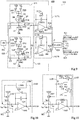
- an oversampling image sensor of an image acquisition system by heterodyne digital holography for example a sensor of the type described in relation to the figures 8 and 9 , especially when the continuous component has 0 ( figure 7 ) of the signal received by a pixel of the sensor is important in front of the alternative component a 1 , it may be advantageous to filter the component a 0 before analog sampling of the signal by the oversampling modulator (formed by blocks 821, 823, 825, 827 and 829 in the example of figure 8 and by blocks 921, 823, 825, 927A, 927B and 829 in the example of the figure 9 ). Examples of circuits adapted to perform this high-pass filtering function will now be described in relation to the figures 10, 11 and 12 .
- the figure 10 shows schematically and partially an embodiment of an image sensor comprising at least one pixel 801 and a circuit 1003 for high-pass filtering of an output signal of this pixel.
- the filtering circuit 1003 can be placed between the output of the pixel 801 and the input VIN of the oversampling modulator of the sensor.
- the pixel 801 comprises a photodiode polarized in reverse by a constant reference voltage VDD, and supplying on its cathode K a current representative of the light intensity received by the pixel.
- the pixel 801 can also include various control elements which are not shown.
- the current supplied by the photodiode comprises a continuous component i dc which corresponds to the continuous component a 0 of the light signal received by the pixel , and an alternative component i ac which corresponds to the alternative component a 1 of the light signal received by the pixel.
- the filter 1003 comprises a differential amplifier 1005 of which a positive input (+) is connected to a node for applying a reference potential, for example to ground, and of which a negative input (-) is connected to the cathode K of the photodiode.
- the differential amplifier 1005 further includes an output node T which can be connected to the node VIN.
- the node T is coupled to the node K by two parallel branches: a first branch comprising a reset switch S20; and a second branch comprising an integration capacitor C5.
- the filter 1003 further comprises a controllable current source 1007 connecting the node K to a node for applying the voltage VDD for biasing the photodiode.
- the filter 1003 further comprises an analog control circuit 1009 (CMD) of the source 1007, one input of which is connected to the node T and one output of which is connected to a control node of the source 1007.
- CMD analog control circuit 1009
- the capacitor C5 charges to a value representative of the average value of the current received on the negative input of the differential amplifier 1005, which is itself equal to the difference between the current delivered by the photodiode and the current delivered by the source 1007.
- the control circuit 1009 controls the current source 1007 so that it delivers a direct current representative of the average of the output signal of the amplifier 1005.
- the output signal supplied on the node T converges towards an alternating voltage centered on a constant average value.
- This AC voltage is representative of the only AC component of the light signal received by the pixel.
- Filter 1003 can be reset by closing switch S20.
- the figure 11 shows schematically and partially another embodiment of an image sensor comprising at least one pixel 801 and a circuit 1103 for high-pass filtering of an output signal of this pixel.
- the filtering circuit 1103 can be placed between the output of the pixel 801 and the input VIN of the oversampling modulator of the sensor.
- pixel 801 is the same or similar to pixel 801 of the figure 10 .
- the filter 1103 comprises, as in the example of the figure 10 , a differential amplifier 1005 whose positive input (+) is connected to a node for applying a reference potential, for example to ground, and whose negative input (-) is connected to the cathode K of the photodiode.
- the node T of output of amplifier 1005 can be connected to the input VIN node of an oversampling modulator.
- the node T is connected to the node K by a resistor R1 or a capacitor (not shown).
- the filter 1103 further comprises a controllable current source 1007 connecting the node K to a node for applying the voltage VDD for biasing the photodiode.
- the filter 1103 further comprises a circuit 1109 for controlling the current source 1007, this circuit comprising an input node L connected to the node T and an output node M connected to a node for controlling the current source 1007.
- the control circuit 1109 comprises a capacitor C6 connecting a node O to a node for applying a reference potential, for example to ground, and a capacitor C7 connecting a node P to a node for applying a potential of reference, for example to mass.
- the circuit 1109 further comprises a switch S21 connecting the node L to the node O, a switch S22 connecting the node O to the node M, a switch S23 connecting the node L to the node P, and a switch S24 connecting the node P to the node M .
- the level of the output signal of the amplifier 1005 can be sampled in the capacitors C6 and C7 at two distinct times phase-shifted by Pi.
- the switches S24 and S22 can be closed, which amounts to applying to the node M a signal representative of the average of the output signal of the amplifier 1005.
- the output signal supplied on the node T converges towards an alternating voltage centered on a constant average value. This AC voltage is representative of the only AC component of the light signal received by the pixel.
- An advantage of the high pass filter circuit of the figure 11 is that it allows an effective amplification of the part alternative i ac of the photodiode output signal.
- the operation of circuit 1103 does not include a reset phase.
- the figure 12 shows schematically and partially another embodiment of an image sensor comprising at least one pixel 801 and a circuit 1203 for high-pass filtering of an output signal of this pixel.
- the filtering circuit 1203 can be placed between the output of the pixel 801 and the input VIN of the oversampling modulator of the sensor.
- pixel 801 is the same or similar to pixel 801 of figures 11 and 12 .
- the filter 1203 comprises, as in the example of the figure 10 , a differential amplifier 1005 whose positive input (+) is connected to a node for applying a reference potential, for example to ground, and whose negative input (-) is connected to the cathode K of the photodiode.
- the output node T of the amplifier 1005 can be connected to the input node VIN of an oversampling modulator.
- the node T is also coupled to the node K by two parallel branches: a first branch comprising a reset switch S20; and a second branch comprising an integration capacitor C5.
- the filter 1203 further comprises a controllable current source 1207 connecting the node K to a node for applying the voltage VDD for biasing the photodiode.
- the current source 1207 is a digitally controlled source.
- the current source 1207 can be controlled by a digital signal corresponding to an output signal from the oversampling analog-to-digital converter. It is for example possible to provide, before the phase of acquisition of the complex field of the object beam at the level of pixel 801, a phase of acquisition of a signal control of the current source 1207.
- An advantage of this exemplary embodiment is that it makes it possible to reuse the hardware of the oversampling sensor and in particular the converter to oversampling to generate a control signal of the current source via a dichotomous search for the mean signal value.
- the current source 1207 comprises m P channel MOS transistors tr 0 , tr 1 , tr 2 , ..., tr m-1 in parallel between the node VDD and the node K, each transistor receiving on its control grid, respectively b 0 , b 1 , b 2 , ..., b m-1 , a bit of the control signal.
- the transistors tr 0 , tr 1 , tr 2 , ..., tr m-1 are of different dimensions, which makes it possible to take into account the weight of the different bits of the control word of the source 1207.
- the transistor tr 0 has a channel width W and a channel length L
- the transistor tr 1 can have a width / length ratio equal to 2 ⁇ W / L
- the transistor tr 2 can have a ratio width / length equal to 4 ⁇ W / L
- the transistor tr m-1 which may have a width / length ratio equal to 2 m-1 ⁇ W / L.
- an advantage of the embodiments described in the present application is that they make it possible to achieve image acquisition systems by heterodyne digital holography in which the constraints linked to the risks of saturation of the pixels of the sensor are very attenuated compared to existing systems.
- the reset frequency of the photodiodes can be significantly higher than in existing systems, which in particular makes it possible to be able to use higher light intensities to illuminate the object to be examined or analyzed.
- Another advantage of the embodiments described is that they make it possible to produce image acquisition systems by heterodyne digital holography having, at the output of the acquisition system, better signal-to-noise ratio than existing systems.
- This improvement in the signal to noise ratio is notably linked to the fact that the use of an analog-digital converter makes it possible to reduce the noise of the quantization system compared to existing systems.
- the improvement in the signal to noise ratio can also be amplified by the use of a high-pass filtering circuit of the type described in relation to the figures 10 to 12 .
- the elimination of the continuous signal before conversion of the residual AC signal makes it possible in particular to focus the quantization resources on the only AC component, which in particular makes it possible to reduce the oversampling factor necessary for obtaining a useful output signal. quantized on a given number of bits.
- the residual error of this filtering phase of the DC component is eliminated by integrating the difference of two samples at the level of the integrator of the Delta Sigma modulator.
- a first method of improving the axial resolution in a system of the type described in relation to the figure 3 we plan to emit the ultrasonic excitation wave by pulses or time slots of duration ⁇ t.
- the acousto-optic modulator MAO1 of the reference channel is then also activated on an impulse basis, during slots of duration ⁇ t, offset by a duration ⁇ relative to the slots of emission of the ultrasonic wave.
- the portion of the sample that can be analyzed by the system is then that excited by the ultrasonic pulse during the time slots where the acousto-optical modulator MAO1 of the reference channel is active.
- the axial resolution of the system is approximately equal to ⁇ t ⁇ V US , where V US is the speed of propagation of the ultrasonic wave in the sample analyzed, and the distance between the ultrasonic emitter and the portion of the sample visible by the system is approximately equal to ⁇ ⁇ V US .
- This first method can be adapted to a system of the type described in relation to the figure 5 , in which the image sensor is an oversampling sensor, and in which the reference channel does not include an acousto-optical modulator.
- the focused ultrasonic wave of excitation of the sample is then, as in the known methods, emitted by pulses or time slots of duration ⁇ t.
- the time slots out of phase with the duration ⁇ fixing the distance between the ultrasonic emitter and the portion of sample actually analyzed cannot be easily applied on the reference channel, the latter not comprising any acousto-optic modulator.
- the modulator of the oversampling converter comprises a node for applying a binary activation signal BURST_ON, defining the time slots for selecting the portion of the sample analyzed.
- BURST_ON a binary activation signal
- the modulator is active, and acquires and processes analog samples of the input signal in an identical or similar manner to what has been described above.
- the modulator is inhibited and stops acquiring samples of the input signal. The effect is then the same as if the slots were applied to the reference channel.
- the BURSTON signal activation slots are preferably synchronous with the operating phases of the sigma-delta modulator. In particular, their duration ⁇ t is preferably equal to a multiple of the converter's oversampling period.
- the figure 13 is a simplified diagram of a control circuit of an analog-digital converter with oversampling of a sensor of the type described in relation to the figures 8 or 9 , suitable for receiving the activation signal BURST_ON, and for controlling the acquisition of samples of the input signal only when the signal BURST_ON is in the active state (high state in this example).
- the circuit of the figure 13 comprises a circuit 1301, clocked by a clock signal CLK, adapted to generate the signals PH1, PH2, PH3 and PH4 for controlling the switches of an oversampling converter of the type described in relation to the figure 8 or 9 (it being understood that in the examples of figures 8 and 9 , the signal PH1 is the control signal of the switches S1 and S5, the signal PH2 is the control signal of the switches S2 and S9, the signal PH3 is the control signal of the switches S3, S6, S14, S15 and S18, and signal PH4 is the control signal of switches S4, S10, S16, S17 and S19).
- the circuit of the figure 13 further comprises an activation circuit 1303 comprising four AND gates 1305 1 , 1305 2 , 1305 3 and 1305 4 each having two binary inputs and a binary output.
- the AND gates 1305 1 , 1305 2 , 1305 3 and 1305 4 receive, on a first input, the signal BURST_ON, and, on a second input, respectively the signals PH1, PH2, PH3 and PH4 generated by the circuit 1301.
- the outputs AND gates 1305 1 , 1305 2 , 1305 3 and 1305 4 provide binary signals PH1 ', PH2', PH3 'and PH4' respectively.
- the signals PH1 ', PH2', PH3 'and PH4' are identical to the signals PH1, PH2, PH3 and PH4 when the signal BURST_ON is in the active state (high state in this example), and are in the low state when the signal BURST_ON is in the inactive state (low state in this example).
- the signals PH1 ', PH2', PH3 'and PH4' are intended to control the switches S1, S5, S2, S9, S3, S6, S14, S15, S18, S4, S10, S16, S17 and S19 to replace the signals PH1, PH2, PH3 and PH4 from the examples of figures 8 and 9 .
- the converter behaves as described above, and acquires samples of the input signal at the oversampling frequency fCs of the sensor.
- switches S1, S5, S2, S9, S3, S6, S14, S15, S18, S4, S10, S16, S17 and S19 are held open, so that the converter stops acquire samples until the next activation of the BURST_ON signal.
- a second method of improving the axial resolution in a system of the type described in relation to the figure 3 provision is made to apply to the excitation ultrasonic wave of the sample a random or pseudo-random sequence of phase jumps of 0 or ⁇ , at a frequency fixing the axial resolution of the system.
- This same phase jump sequence is also applied to the reference channel by means of the MAO1 acousto-optical modulator, with a time offset of duration ⁇ with respect to the sequence applied to the ultrasonic wave.
- the portion of sample seen by the system is then that in which the sequence of phase jumps applied to the ultrasonic wave coincides temporally with the sequence of phase jumps applied to the reference beam.
- the axial resolution of the system is approximately equal to ⁇ t ⁇ V US , where ⁇ t is the period of application of the phase jumps and V US is the speed of propagation of the ultrasonic wave in the sample analyzed, and the distance between the ultrasonic transmitter and the portion of the sample visible to the sensor is approximately equal to ⁇ * V US .
- This second method can be adapted to a system of the type described in relation to the figure 5 , in which the sensor of images is an oversampling sensor, and in which the reference channel does not include an acousto-optical modulator.
- a random or pseudo-random sequence of phase jumps of 0 or ⁇ , at a rate 1 / ⁇ t fixing the axial resolution of the system, is then applied to the ultrasonic wave.
- the same sequence phase shifted by a duration ⁇ fixing the distance between the ultrasonic emitter and the portion of sample analyzed, cannot easily be applied to the reference channel, the latter not comprising acousto-optic modulator.
- the figure 14 is a simplified diagram of a control circuit of an analog-digital converter with oversampling of a sensor of the type described in relation to the figures 8 or 9 , adapted to receive a random binary signal PHASE_JUMP representative of a sequence of phase jumps identical to that applied to the ultrasonic wave, but offset by the duration ⁇ relative to the sequence applied to the ultrasonic wave, and to order phase reversals in the sample acquisition sequence of the input signal each time the PHASE_JUMP signal changes state.
- the high state of the PHASE_JUMP signal corresponds to a phase shift of ⁇
- the low state of the PHASE_JUMP signal corresponds to a zero phase shift.
- the circuit of the figure 14 comprises a circuit 1301, clocked by a clock signal CLK, adapted to generate the signals PH1, PH2, PH3 and PH4 for controlling the switches of an oversampling converter of the type described in relation to the figure 8 or 9 .
- the circuit of the figure 14 further comprises a phase inversion circuit 1403 comprising four multiplexers 1405 1 , 1405 2 , 1405 3 and 1405 4 from two inputs to an output.
- the multiplexer 1405 1 receives respectively on its first and second inputs signals PH1 and PH3
- multiplexer 1405 2 receives respectively on its first and second inputs signals PH2 and PH4
- multiplexer 1405 3 receives respectively on its first and second inputs signals PH3 and PH1
- the multiplexer 1405 4 receives respectively on its first and second inputs the signals PH4 and PH2.
- the multiplexers 1405 1 , 1405 2 , 1405 3 and 1405 4 respectively supply binary signals PH1 ', PH2', PH3 'and PH4' on their outputs.
- Each multiplexer further comprises a selection input receiving the PHASE_JUMP signal.
- the signals PH1 ', PH2', PH3 'and PH4' are identical to the signals PH1, PH2, PH3 and PH4 when the signal PHASE_JUMP is in the low state (zero phase shift), and the signals PH1 ', PH2', PH3 ' and PH4 'are respectively identical to the signals PH3, PH4, PH1 and PH2 when the signal PHASE_JUMP is in the high state (phase shift equal to ⁇ ).
- the operating phases PH1 and PH3, respectively PH2 and PH4 of the oversampling converter are inverted. It will be noted that, in this example, it is necessary to respect a temporal coherence between the frequency 1 / ⁇ t of application of the phase jumps, and the sampling phases PH1, PH2, PH3 and PH4 of the pixels.
- the embodiments described are not limited to the specific examples of oversampling image sensors described in relation to the figures 8 and 9 . More generally, those skilled in the art will be able to obtain the desired operation by using other architectures of oversampling image sensors. Those skilled in the art will also be able to adapt the architectures described in the case where the ratio n between the beat frequency f B of the system and the oversampling frequency f Cs of the sensor is different from 4, and where the formulas for reconstruction of the complex field of the object beam are different from the formulas mentioned above.
Landscapes
- Engineering & Computer Science (AREA)
- Theoretical Computer Science (AREA)
- Physics & Mathematics (AREA)
- General Physics & Mathematics (AREA)
- Computing Systems (AREA)
- Investigating Or Analysing Materials By Optical Means (AREA)
- Analogue/Digital Conversion (AREA)
- Optical Radar Systems And Details Thereof (AREA)
Description
- La présente demande de brevet revendique la priorité de la demande de brevet français
FR13/63761 - La présente demande concerne le domaine de l'acquisition d'images, et vise plus particulièrement un système d'acquisition d'images par holographie numérique hétérodyne.
- On désigne généralement par holographie numérique des techniques permettant d'enregistrer, à l'aide d'un capteur d'images numériques, la phase et l'amplitude d'un faisceau de lumière cohérente après réflexion ou transmission par un objet.
- Les techniques d'holographie usuelles sont basées sur l'utilisation des interférences produites par la superposition de deux faisceaux lumineux cohérents, le premier, ou faisceau objet, étant transmis ou réfléchi par l'objet à examiner, et le deuxième, ou faisceau de référence, ne passant pas par l'objet à examiner.
- L'holographie hétérodyne est une technique d'holographie dans laquelle le faisceau objet et le faisceau de référence sont légèrement décalés en fréquence. Un exemple de système d'acquisition d'image par holographie numérique hétérodyne est par exemple décrit dans l'article intitulé "Numerical heterodyne holography with two-dimensionnal photodetector arrays" de F. Le Clerc et al.
- Il existe un besoin d'améliorer au moins en partie certains aspects des systèmes existants d'acquisition d'images par holographie numérique hétérodyne.
- Pour cela, un mode de réalisation prévoit un système d'acquisition d'images par holographie numérique hétérodyne, comportant : un capteur d'images ayant au moins une photodiode couplée à un convertisseur analogique-numérique ; et un montage optique permettant de projeter simultanément sur le capteur des premier et deuxième faisceaux lumineux cohérents de fréquences distinctes, dans lequel le convertisseur est adapté à acquérir, à une première fréquence, des échantillons analogiques représentatifs d'un signal de sortie de la photodiode, à produire, à une deuxième fréquence égale à la première fréquence ou à un sous-multiple de la première fréquence, des premiers échantillons numériques d'une première résolution à partir desdits échantillons analogiques, et à fournir, à une troisième fréquence égale à un sous-multiple de la deuxième fréquence, des deuxièmes échantillons numériques de résolution supérieure à la première résolution, générés à partir des premiers échantillons numériques, et dans lequel la première fréquence du convertisseur est égale à un nombre entier n de fois la fréquence de battement du système, c'est-à-dire la valeur absolue de la différence entre les fréquences des premier et deuxième faisceaux.
- Selon un mode de réalisation, le montage optique comprend un unique modulateur acousto-optique.
- Selon un mode de réalisation, le montage optique ne comprend pas de modulateur acousto-optique, et comprend une source ultrasonore d'excitation d'un objet par lequel passe le deuxième faisceau lumineux.
- Selon un mode de réalisation, la source ultrasonore est adaptée à émettre une onde ultrasonore pendant un premier intervalle de temps de durée Δt, et le convertisseur est adapté à n'acquérir des échantillons représentatifs d'un signal de sortie de la photodiode que pendant un deuxième intervalle de temps de même durée Δt, décalé temporellement par rapport au premier intervalle de temps.
- Selon un mode de réalisation, la source ultrasonore est adaptée à émettre une onde ultrasonore présentant une première séquence aléatoire ou pseudo-aléatoire de sauts de phase de 0 ou π, et le convertisseur est adapté à recevoir un signal binaire représentatif d'une deuxième séquence de sauts de phase identique à la première séquence mais décalée temporellement par rapport à la première séquence, et à modifier une séquence de traitement des échantillons analogiques en fonction de ce signal binaire.
- Selon un mode de réalisation, n est égal à 4.
- Selon un mode de réalisation, le convertisseur comprend un bloc d'échantillonnage analogique adapté à acquérir n échantillons analogiques d'un signal de sortie de la photodiode à chaque période de battement du système.
- Selon un mode de réalisation, le bloc d'échantillonnage analogique est adapté à effectuer en analogique, à chaque période de battement une ou plusieurs opérations arithmétiques à partir desdits échantillons.
- Selon un mode de réalisation, le convertisseur est adapté à fournir, après un nombre entier N de périodes de battement du système, un premier signal numérique sur m bits, représentatif de la partie réelle du champ complexe du deuxième faisceau lumineux, et un deuxième signal numérique sur m bits, représentatif de la partie imaginaire du champ complexe du deuxième faisceau lumineux, où m est un nombre entier supérieur ou égal à 1.
- Selon un mode de réalisation, m est égal à log2.
- Selon un mode de réalisation, le convertisseur comprend un intégrateur comportant deux capacités d'intégration.
- Selon un mode de réalisation, le convertisseur comprend deux intégrateurs comportant chacun une capacité d'intégration.
- Selon un mode de réalisation, le capteur comporte en outre un circuit de filtrage passe-haut entre la photodiode et le convertisseur.
- L'invention est définie plus précisément par les revendications ci-jointes.
- Ces caractéristiques et leurs avantages, ainsi que d'autres, seront exposés en détail dans la description suivante de modes de réalisation particuliers faite à titre non limitatif en relation avec les figures jointes parmi lesquelles :
- la
figure 1 représente de façon schématique un exemple d'un système d'acquisition d'images par holographie numérique hétérodyne ; - la
figure 2 est un diagramme illustrant un exemple de fonctionnement du système de lafigure 1 ; - la
figure 3 représente de façon schématique un autre exemple d'un système d'acquisition d'images par holographie numérique hétérodyne ; - la
figure 4 représente de façon schématique un exemple d'un mode de réalisation d'un système d'acquisition d'images par holographie hétérodyne ; - la
figure 5 représente de façon schématique un autre exemple d'un mode de réalisation d'un système d'acquisition d'images par holographie hétérodyne ; - les
figures 6A et 6B représentent de façon schématique un exemple de réalisation d'un convertisseur analogique-numérique à sur-échantillonnage de type sigma-delta ; - la
figure 7 est un diagramme illustrant de façon schématique un exemple de fonctionnement d'un mode de réalisation d'un système d'acquisition d'images par holographie numérique hétérodyne ; - la
figure 8 représente de façon schématique et partielle un exemple d'un mode de réalisation d'un capteur d'images d'un système d'acquisition d'images par holographie numérique hétérodyne ; - la
figure 9 représente de façon schématique et partielle une variante de réalisation d'un capteur d'images d'un système d'acquisition d'images par holographie numérique hétérodyne ; et - les
figures 10 à 12 représentent de façon schématique et partielle d'autres variantes de réalisation d'un capteur d'images d'un système d'acquisition d'images par holographie numérique hétérodyne. - Par souci de clarté, de mêmes éléments ont été désignés par de mêmes références aux différentes figures et, de plus, les diverses figures ne sont pas tracées à l'échelle. Par ailleurs, seuls les éléments utiles à la compréhension des modes de réalisation décrits ont été détaillés. En particulier, les diverses utilisations qui peuvent être faites d'un système d'acquisition d'image par holographie numérique hétérodyne n'ont pas été détaillées, les modes de réalisation décrits étant compatibles avec toutes les applications connues de l'holographie numérique hétérodyne.
- La
figure 1 représente de façon schématique un exemple d'un système 100 d'acquisition d'images par holographie numérique hétérodyne. - Le système 100 comprend une source lumineuse 101 (L) adaptée à générer un faisceau lumineux cohérent de fréquence fL, par exemple une source laser. Le système 100 comprend en outre un séparateur 103, par exemple une lame 103 partiellement transparente et partiellement réfléchissante placée à 45 degrés par rapport à la direction d'émission de la source 101, permettant de diviser en deux parties le faisceau produit par la source 101. En sortie du séparateur 103, une première partie de faisceau, ou faisceau de référence R, est modulée par un premier modulateur acousto-optique MAO1 décalant sa fréquence d'une valeur fMAO1, et une deuxième partie de faisceau, ou faisceau objet O, est modulée par un deuxième modulateur acousto-optique MAO2 décalant sa fréquence d'une valeur fMAO2 différente de la valeur fMAO1. Le système est agencé de façon que le faisceau objet, de fréquence fL+fMAO2, illumine un objet 105 (OBJ) à examiner, le faisceau de référence, de fréquence fL+fMAO1, ne passant pas par l'objet 105. Le faisceau de référence et le faisceau objet réfléchi ou transmis par l'objet 105 sont ensuite dirigés vers un élément de recombinaison 107, par exemple une lame partiellement réfléchissante et partiellement transparente qui les recombine. Le faisceau résultant fourni par l'élément 107, comportant à la fois le signal objet et le signal de référence, est projeté sur un capteur d'images 109 comportant une matrice de pixels (non visibles sur la
figure 1 ). - En fonctionnement, le capteur 109 voit une figure d'interférences présentant une fréquence de battement fB égale à la valeur absolue de la différence de fréquence entre le faisceau objet et le faisceau de référence, c'est-à-dire à la valeur absolue de la différence fMAO2-fMAO1.
- La
figure 2 est un diagramme illustrant plus en détail le principe de fonctionnement du système de lafigure 1 . - Le diagramme de la
figure 2 comprend une courbe 201 représentant l'évolution en fonction du temps de l'intensité lumineuse I reçue par un pixel du capteur 109 du système de lafigure 1 , lorsque le capteur 109 est éclairé par le faisceau fourni par l'élément 107, combinant le faisceau objet de fréquence fL+fMAO2 et le faisceau de référence de fréquence fL+fMAO1. Comme cela apparaît sur la figure, l'intensité I reçue évolue de façon sinusoïdale autour d'une valeur moyenne ou composante continue a0, avec une amplitude de crête de valeur a1, à une fréquence égale à la fréquence de battement fB du système. Les intensités lumineuses reçues par différents pixels du capteur 109 peuvent avoir des composantes continues a0 distinctes et/ou des amplitudes a1 distinctes, mais fluctuent toutes de façon sinusoïdale à la fréquence de battement fB, avec des déphasages propres. - Dans cet exemple, la fréquence d'acquisition fC du capteur d'images 109 est égale à quatre fois la fréquence de battement fB du système. Ainsi, pour un pixel donné, le capteur 109 fournit quatre valeurs de sortie I1, I2, I3 et I4 en une période de battement TB = 1/fB du système.
- Lorsque quatre valeurs de sorties successives déphasées de π/2, c'est-à-dire séparées d'un intervalle de temps TB/4, ont été acquises pour chaque pixel du capteur, c'est-à-dire lorsque quatre images successives ont été acquises par le capteur, le champ complexe EO du faisceau objet reçu par le capteur 109 peut être déterminé, pour chaque pixel du capteur, par la formule EO = (I1-I3) + j (I2-I4). La composante I1-I3 correspond à la partie réelle du champ EO, et la composante I2-I4 correspond à la partie imaginaire du champ EO. La phase PO et l'amplitude AO du signal objet reçu par chaque pixel du capteur peuvent être déterminées par les formules suivantes :


- On notera que le ratio n entre la fréquence de battement fB du système et la fréquence d'acquisition fC du capteur d'images peut être un nombre entier différent de 4, par exemple n = 2, n = 3, ou n = 5. Dans ce cas, le principe de fonctionnement est similaire à ce qui a été décrit précédemment, c'est-à-dire que, pour chaque pixel, le capteur acquiert n valeurs de sortie déphasées de 2π/n en une période de battement TB = 1/fB, puis ces valeurs sont utilisées pour déterminer, pixel par pixel, par des formules de calcul adaptées (différentes des formules mentionnées ci-dessus pour le cas n=4), l'amplitude AO et la phase PO du faisceau objet reçu par le capteur.
- La
figure 3 représente de façon schématique un autre exemple d'un système 300 d'acquisition d'images par holographie numérique hétérodyne. Le système 300 comprend des éléments communs avec le système 100 de lafigure 1 . Seules les différences entre ces deux systèmes seront détaillées ci-après. - Le système 300 comprend, comme le système 100 de la
figure 1 , une source lumineuse 101, un séparateur 103 adapté à diviser un faisceau fourni par la source 101 en un faisceau objet et un faisceau de référence, un premier modulateur acousto-optique MAO1 adapté à décaler la fréquence du faisceau de référence d'une valeur fMAO1, et un deuxième modulateur acousto-optique MAO2 adapté à décaler la fréquence du faisceau objet d'une valeur fMAO2. Le système 300 est agencé de façon que le faisceau objet, de fréquence fL+fMAO2, illumine un objet ou échantillon 305 à analyser, et que le faisceau de référence, de fréquence fL+fMAO1, ne passe pas par l'objet 305. - Dans le système 300, une partie de l'objet ou échantillon 305 est excitée par une onde ultrasonore focalisée de fréquence fUS. Il en résulte que la fréquence des rayons du faisceau objet passant par la partie excitée de l'échantillon est décalée à la valeur fL+fMAO2+fUS, alors que la fréquence des rayons du faisceau objet passant par les parties non-excitées de l'échantillon reste à la valeur fL+fMAO2. Ce décalage fréquentiel permet de "marquer" les photons du faisceau objet passés par la partie excitée de l'échantillon par rapport aux autres photons du faisceau objet.
- Le faisceau de référence et le faisceau objet sont ensuite dirigés vers un élément de recombinaison 107. Le faisceau résultant fourni par l'élément 107, comportant à la fois le signal objet et le signal de référence, est projeté sur un capteur d'images 109.
- Dans le système 300, la fréquence de battement fB du système est définie comme étant la valeur absolue de la différence de fréquence entre le faisceau de référence et la portion du faisceau objet passée par la partie excitée de l'échantillon 305. Ainsi, la fréquence de battement fB du système 300 est égale à la valeur absolue de la différence fMAO2+fUS-fMAO1. La fréquence d'acquisition fC du capteur d'images 109 est, comme dans l'exemple précédent, égale à n fois la fréquence de battement fB du système, où n est un nombre entier, par exemple égal à quatre.
- Le principe de fonctionnement du système 300 est similaire à ce qui a été décrit précédemment en relation avec les
figures 1 et 2 , c'est-à-dire que, pour chaque pixel, le capteur acquiert n valeurs de sortie successives déphasées de 2π/n en une période de battement TB = 1/fB du système. Ces valeurs de sortie sont ensuite utilisées pour déterminer, pixel par pixel, au moyen de formules de calcul adaptées, le champ complexe de la partie de faisceau objet modulée par l'échantillon 305, et en déduire des informations sur la portion excitée de l'échantillon 305. - Un exemple plus détaillé de réalisation d'un système utilisant la technique du marquage ultrasonore de la lumière combinée avec la technique de l'holographie numérique hétérodyne est décrit dans l'article intitulé "Acousto-Optical Coherence Tomography with a digital holographic détection scheme" de Emilie Benoit a la Guillaume et al.
- Un inconvénient des systèmes d'acquisition d'images par holographie numérique hétérodyne du type décrit en relation avec les
figures 1 à 3 réside dans la complexité, le coût, et l'encombrement des modulateurs acousto-optiques. De plus, les modulateurs acousto-optiques entrainent une atténuation relativement importante des faisceaux lumineux, ce qui oblige à prévoir une source d'éclairement 101 relativement puissante. - On notera que les modulateurs acousto-optiques usuels peuvent typiquement décaler la fréquence d'un faisceau lumineux d'une valeur de l'ordre de quelques MHz à quelques dizaines de MHz, par exemple d'une valeur comprise entre 5 et 100 MHz. De plus, dans le système de la
figure 3 , l'excitation ultrasonore d'une partie de l'objet à analyser peut provoquer un décalage de fréquence de la lumière passant par la partie excitée de l'objet d'une valeur comprise entre quelques centaines de kHz et quelques MHz, par exemple d'une valeur comprise entre 1 et 15 MHz. Or, la fréquence d'acquisition fC des capteurs d'image usuels est typiquement comprise entre quelques dizaines de Hz et quelques dizaines de kHz, par exemple entre 20 Hz et 20 kHz. C'est pour ces raisons que, dans les systèmes du type décrit en relation avec lesfigures 1 à 3 , pour obtenir une fréquence de battement fB inférieure d'un facteur n à la fréquence d'acquisition fC du capteur (fB = fC/n), on prévoit deux modulateurs acousto-optique. En effet, même s'il serait possible d'obtenir des interférences entre le faisceau objet et le faisceau de référence avec un seul modulateur acousto-optique dans le système de lafigure 1 , ou sans modulateur acousto-optique dans le système de lafigure 3 , la fréquence de battement de ces interférences serait alors bien trop élevée par rapport à la fréquence d'acquisition du capteur d'images pour pouvoir mettre en oeuvre un fonctionnement du type décrit en relation avec lafigure 2 . - A titre d'exemple numérique illustratif et non limitatif : dans le système de la
figure 1 , le capteur 109 peut avoir une fréquence d'acquisition fC de 8 kHz, et les décalages fréquentiels fMAO1 et fMAO2 introduits par les modulateurs MAO1 et MAO2 peuvent être respectivement de 79,999 MHz et de 80,001 MHz pour obtenir une fréquence de battement fB = fMAO2-fMAO1 = 2 kHz = fC/4 ; et, dans le système de lafigure 3 , le capteur 109 peut avoir une fréquence d'acquisition fC de 8 kHz, et les décalages fréquentiels fMAO1, fMAO2 et fUS introduits par les modulateurs MAO1 et MAO2 et par l'onde ultrasonore d'excitation de l'échantillon 305 peuvent être respectivement de 79,999 MHz, 77,001 MHz et 3 MHz, pour obtenir une fréquence de battement fB = fMAO2 + fUS - fMAO1 = 2 kHz = fC/4. - Un autre inconvénient des systèmes d'acquisition d'images par holographie numérique hétérodyne du type décrit en relation avec les
figures 1 à 3 est lié aux seuils de saturation des pixels du capteur, qui limitent la puissance lumineuse qui peut être reçue par le capteur. En effet, la puissance lumineuse reçue par chaque pixel du capteur doit être suffisamment faible pour ne pas risquer de saturer le pixel avant la fin d'une période d'intégration TB/n du pixel, ce qui peut poser problème dans certaines applications. - Un autre inconvénient des systèmes du type décrit en relation avec les
figures 1 à 3 est que le rapport signal sur bruit en sortie du système est relativement faible, notamment en raison du fait qu'une part importante des charges photogénérées dans chaque pixel pendant une période d'intégration TB/n du pixel correspond à la composante continue a0 du signal, qui n'est plus exploitée après la reconstruction du signal objet. A titre d'exemple, dans le système décrit en relation avec lesfigures 1 et 2 , la composante continue a0 de l'intensité I reçue par un pixel du capteur 109 est égale à la somme de l'intensité lumineuse I0 du faisceau objet au niveau de ce pixel et de l'intensité lumineuse IR du faisceau de référence au niveau de ce pixel, et l'amplitude de crête a1 de l'intensité I reçue par le pixel s'exprime par la formule
- Un objet des modes de réalisation décrits ci-après est de prévoir un système d'acquisition d'images par holographie numérique hétérodyne permettant de pallier tout ou partie des inconvénients susmentionnés.
- Selon un aspect des modes de réalisation décrits, on prévoit un système d'acquisition d'images par holographie numérique hétérodyne, comportant un capteur d'images à sur-échantillonnage, c'est-à-dire un capteur d'images ayant au moins une photodiode couplée à un convertisseur analogique-numérique à sur-échantillonnage, par exemple un convertisseur de type sigma-delta.
- Comme cela sera expliqué plus en détail ci-après, l'utilisation d'un capteur d'images à sur-échantillonnage dans un système d'acquisition d'images par holographie numérique hétérodyne permet de réaliser un système fonctionnant avec une fréquence de battement fB = fCs/n, où fCs est la fréquence de sur-échantillonnage du capteur. A titre d'exemple, la fréquence de sur-échantillonnage fCs peut être comprise entre 1 MHz et 100 MHz. On peut donc réaliser un système fonctionnant avec une fréquence de battement fB de l'ordre de plusieurs MHz à plusieurs dizaines de MHz. Ceci permet de réaliser un système d'acquisition d'images par holographie numérique hétérodyne particulièrement simple, peu coûteux et peu encombrant. En particulier, ceci permet, comme illustré par les
figures 4 et 5 , d'économiser un modulateur acousto-optique par rapport à un système du type décrit en relation avec lafigure 1 , ou deux modulateurs acousto-optiques par rapport à un système décrit en relation avec lafigure 3 . - La
figure 4 représente de façon schématique un exemple d'un mode de réalisation d'un système 400 d'acquisition d'images par holographie numérique hétérodyne. Le système 400 comprend des éléments communs avec le système 100 de lafigure 1 . Seules les différences entre les systèmes 100 de lafigure 1 et 400 de lafigure 4 seront détaillées par la suite. - Le système 400 comprend, comme le système 100 de la
figure 1 , une source lumineuse 101 adaptée à générer un faisceau lumineux cohérent de fréquence fL, et un séparateur 103 adapté à diviser un faisceau fourni par la source 101 en un faisceau objet O et un faisceau de référence R. Dans l'exemple de lafigure 4 , le faisceau objet O est modulé par un modulateur acousto-optique MAO1 décalant sa fréquence d'une valeur fMAO1, par exemple comprise entre 5 et 100 MHz, et le faisceau de référence R n'est pas modulé par un modulateur acousto-optique et reste donc à la fréquence fL. A titre de variante, le modulateur acousto-optique MAO1 peut être agencé pour moduler le faisceau de référence R et pas le faisceau objet O. Le système 400 est agencé de façon que le faisceau objet, de fréquence fL+fMAO1, illumine un objet 105 (OBJ) à examiner ou analyser, le faisceau de référence, de fréquence fL, ne passant pas par l'objet 105. Le faisceau de référence et le faisceau objet réfléchi ou transmis par l'objet 105 sont ensuite dirigés vers un élément de recombinaison 107 qui les recombine. Le faisceau résultant fourni par l'élément 107, comportant à la fois le signal objet et le signal de référence, est projeté sur un capteur d'images 409 à sur-échantillonnage, comportant un ou plusieurs pixels (non visibles sur lafigure 4 ), par exemple une matrice de pixels, chaque pixel comportant une photodiode couplée à un convertisseur analogique-numérique à sur-échantillonnage. - En fonctionnement, le capteur 409 voit une figure d'interférences présentant une fréquence de battement fB égale à la valeur absolue de la différence de fréquence entre le faisceau objet et le faisceau de référence, c'est-à-dire égale à la valeur fMAO1. La fréquence de battement fB = fMAO1 du système est choisie telle que la fréquence de sur-échantillonnage fCs du capteur 409 soit égale à un nombre n entier de fois la fréquence de battement fB, par exemple fCs = 4∗fB.
- La
figure 5 représente de façon schématique un exemple d'un mode de réalisation d'un système 500 d'acquisition d'images par holographie numérique hétérodyne. Le système 500 comprend des éléments communs avec le système 300 de lafigure 3 . Seules les différences entre les systèmes 300 de lafigure 3 et 500 de lafigure 5 seront détaillées par la suite. - Comme le système 300 de la
figure 3 , le système 500 comprend une source lumineuse 101 adaptée à générer un faisceau lumineux cohérent de fréquence fL, et un séparateur 103 adapté à diviser un faisceau fourni par la source 101 en un faisceau objet O et un faisceau de référence R. Le système 500 est agencé de façon que le faisceau objet O illumine un objet ou échantillon 305 à analyser, et que le faisceau de référence ne passe pas par l'objet 305. Dans l'exemple de lafigure 5 , le faisceau de référence n'est pas modulé par un modulateur acousto-optique et reste donc à la fréquence fL, et le faisceau objet n'est pas modulé par un modulateur acousto-optique et reste donc aussi à la fréquence fL avant d'atteindre l'objet 305. Dans le système 500, une partie de l'objet ou échantillon 305 est excitée par une onde ultrasonore focalisée de fréquence fUS, par exemple comprise entre 1 et 15 MHz. Il en résulte que la fréquence des rayons du faisceau objet passant par la partie excitée de l'échantillon est décalée à la valeur fL+fUS, alors que la fréquence des rayons du faisceau objet passant par les parties non-excitées de l'échantillon reste à la valeur fL. Ce décalage fréquentiel permet, de façon similaire à ce qui a été décrit dans l'exemple de lafigure 3 , de "marquer" les photons du faisceau objet passés par la partie excitée de l'échantillon par rapport aux autres photons du faisceau objet. Le faisceau de référence et le faisceau objet sont ensuite dirigés vers un élément de recombinaison 107. Le faisceau résultant fourni par l'élément 107, comportant à la fois le signal objet et le signal de référence, est projeté sur un capteur d'images à sur-échantillonnage 409 qui peut être identique ou similaire à celui de lafigure 4 . - En fonctionnement, le capteur 409 voit une figure d'interférences présentant une fréquence de battement fB égale à la valeur absolue de la différence de fréquence entre le faisceau de référence et la portion du faisceau objet passée par la partie excitée de l'échantillon 305, c'est-à-dire égale à la valeur fUS. La fréquence de battement fB = fUS du système 500 est choisie telle que la fréquence de sur-échantillonnage fCs du capteur 409 soit égale à un nombre n entier de fois la fréquence de battement fB, par exemple fCs = 4∗fB.
- Les
figures 6A et 6B représentent schématiquement, sous forme de blocs, un exemple de réalisation d'un convertisseur analogique-numérique à sur-échantillonnage 600 de type sigma-delta. Lafigure 6A est une vue d'ensemble du convertisseur 600, et lafigure 6B représente de façon plus détaillée un bloc de modulation du convertisseur 600. - Le convertisseur 600 comprend une entrée IN adaptée à recevoir un signal analogique à numériser, et une sortie OUT adaptée à fournir, à une fréquence d'échantillonnage fe, des échantillons de sortie numérisés sur m-bits, où m est un nombre entier supérieur ou égal à 1.
- Le convertisseur 600 comprend un modulateur à sur-échantillonnage 601 (ΔΣ MODULATOR) qui reçoit en entrée le signal analogique appliqué sur l'entrée IN du convertisseur, et fournit en sortie une suite d'échantillons intermédiaires basse résolution, des échantillons de 1-bit dans cet exemple, à une fréquence de sur-échantillonnage fs plus élevée que la fréquence d'échantillonnage fe, par exemple égale à un multiple de la fréquence d'échantillonnage fe.
- Le modulateur 601 est représenté de façon plus détaillée en
figure 6B . Il comprend un circuit analogique de soustraction 611 à deux entrées, respectivement positive (+) et négative (-), et une sortie. Ce circuit peut par exemple être constitué par un montage à capacités commutées. L'entrée positive du circuit 611 est reliée à l'entrée IN du convertisseur 600, et la sortie du circuit 611 est reliée à une entrée d'un intégrateur analogique 613, qui peut par exemple comprendre un condensateur en contre-réaction d'un amplificateur. Le modulateur 601 comprend en outre un comparateur 615 cadencé à la fréquence de sur-échantillonnage fs du convertisseur. Le comparateur 615 a une première entrée reliée à une sortie de l'intégrateur 613, et une deuxième entrée adaptée à recevoir un signal de référence VREF. La sortie du comparateur 615 correspond dans cet exemple à la sortie du modulateur 601. En fonctionnement, le comparateur 615 compare, à la fréquence fs, le signal de sortie de l'intégrateur 613 au signal de référence VREF, et fournit un signal de sortie numérique sur 1-bit correspondant au résultat de la comparaison. La sortie du comparateur 615 est de plus reliée à l'entrée d'un convertisseur numérique-analogique 1-bit 617, la sortie du convertisseur 617 étant reliée à l'entrée négative du circuit 611. - Le convertisseur 600 comprend en outre un filtre numérique 603 (FILTER) qui reçoit en entrée les échantillons intermédiaires de 1-bit fournis par le modulateur 601, et fournit à sa sortie, à la fréquence de sur-échantillonnage fs, une suite d'échantillons intermédiaires numériques de p-bits par échantillon, où p est un nombre entier supérieur ou égal à m. Le filtre 603 a notamment pour fonction de générer des échantillons haute résolution représentatifs du signal analogique d'entrée à partir des échantillons de 1-bit fournis par le modulateur 601, et de réaliser un filtrage passe-bas permettant de supprimer en grande partie le bruit introduit par le modulateur 601. A titre d'exemple, le filtre 603 comprend un intégrateur numérique d'ordre 1, c'est-à-dire un compteur qui effectue une sommation d'échantillons successifs du signal de sortie du modulateur 601. Dans ce cas particulier, le nombre p de bits des échantillons intermédiaires en sortie du filtre 603 est égal au nombre m de bits des échantillons de sortie du convertisseur 600.
- Le convertisseur 600 comprend en outre un circuit de sous-échantillonnage 605 (DECIMATOR) qui reçoit en entrée les échantillons intermédiaires de p-bits fournis par le filtre 603 à la fréquence fs, et fournit en sortie une suite d'échantillons de sortie de m-bits par échantillon, à la fréquence d'échantillonnage fe ou fréquence de sortie du convertisseur 600. La sortie du circuit de sous-échantillonnage 605 est reliée à la sortie OUT du convertisseur 600.
- La
figure 7 est un diagramme illustrant de façon schématique un exemple de fonctionnement d'un système d'acquisition d'images par holographie numérique hétérodyne comportant un capteur d'images à sur-échantillonnage, par exemple un système du type décrit en relation avec lafigure 4 ou 5 . - Le diagramme de la
figure 7 comprend une courbe 701 représentant l'évolution, en fonction du temps, de l'intensité lumineuse I reçue par un pixel du capteur 409 du système, lorsque le capteur 409 est éclairé par le faisceau fourni par l'élément 107, combinant le faisceau objet et le faisceau de référence. Comme cela apparaît sur la figure, l'intensité I reçue évolue de façon sinusoïdale autour d'une valeur moyenne ou composante continue a0, avec une amplitude de crête de valeur a1, à une fréquence égale à la fréquence de battement fB du système (fB = fMAO1 dans l'exemple de lafigure 4 et fB = fUS dans l'exemple de lafigure 5 ) . Les intensités lumineuses reçues par différents pixels du capteur 409 peuvent avoir des composantes continues a0 distinctes et/ou des amplitudes a1 distinctes, mais fluctuent toutes de façon sinusoïdale à la fréquence de battement fB, avec des déphasages propres. - Dans cet exemple, la fréquence de sur-échantillonnage fCs du capteur d'images 409 est égale à n=4 fois la fréquence de battement fB du système. A la différence des systèmes des
figures 1 à 3 dans lesquels, pour un pixel donné du capteur 109, l'acquisition du champ complexe du faisceau objet au niveau du pixel peut être effectuée en une période de battement TB du système, dans le mode de réalisation de lafigure 7 , pour un pixel donné du capteur 409, une acquisition du champ complexe du faisceau objet reçu au niveau du pixel s'effectue en N périodes de battement TB, où N est un nombre entier supérieur à 1. - A chaque période de battement TB d'une période N∗TB d'acquisition du champ complexe du faisceau objet au niveau du pixel, quatre valeurs analogiques de sortie du pixel i1i, i2i, i3i et i4i sont acquises à des instants successifs décalés de TB/4 (c'est-à-dire avec un déphasage de π/2), où i est un nombre entier allant de 1 à N. On se ramène ainsi, dans cet exemple à l'observation, pendant la période d'acquisition N∗TB, de quatre signaux continus il, i2, i3 et i4 échantillonnés à la fréquence fB. On notera que si le pixel fournit un signal représentatif d'une accumulation de charges photogénérées dans sa photodiode, la photodiode du pixel peut être réinitialisée entre deux acquisitions successives d'une valeur analogique de sortie du pixel. Si en revanche la photodiode du pixel est polarisée à une tension de référence fixe et si le pixel fournit un signal représentatif d'un photo-courant circulant dans la photodiode, le pixel peut ne pas être réinitialisé entre deux acquisitions successives d'une valeur analogique de sortie du pixel. Un convertisseur analogique-numérique à sur-échantillonnage couplé à la photodiode du pixel, par exemple un convertisseur de type sigma-delta, peut fournir, à l'issue de la période d'acquisition N∗TB, pour chacun des signaux continus il, i2, i3 et i4 observés, un échantillon numérique de m bits représentatif du niveau du signal, où m est un nombre entier supérieur à 1, par exemple compris dans la plage allant de 8 à 24. A titre d'exemple, le nombre m de bits des échantillons de sortie peut être égal à log2(N) pour un modulateur delta sigma d'ordre 1. Pour chaque pixel du capteur, le champ complexe EO du faisceau objet reçu par le capteur peut être déterminé par la formule EO = (i1-i3) + j(i2-i4), la composante i1-i3 correspondant à la partie réelle du champ EO, et la composante i2-i4 correspondant à la partie imaginaire du champ EO. La phase PO et l'amplitude AO du signal objet reçu par chaque pixel du capteur peuvent être déterminées par les formules suivantes :


- On notera que le ratio n entre la fréquence de battement fB du système et la fréquence de sur-échantillonnage fCs du capteur d'images peut être un nombre entier différent de 4, par exemple n = 2, n = 3, ou n = 5. Dans ce cas, le principe de fonctionnement est similaire à ce qui a été décrit précédemment, mais les formules de reconstruction du champ complexe du signal objet sont différentes.
- Dans l'exemple susmentionné où n=4, afin de réduire les contraintes sur la gamme dynamique du convertisseur analogique-numérique à sur-échantillonnage, les opérations de soustraction i1-i3 et i2-i4 peuvent être effectuées avant la fourniture des échantillons numérisés sur m bits, par exemple au moment de l'acquisition des valeurs analogiques i1i, i2i, i3i et i4i comme cela sera expliqué plus en détail en relation avec les exemples de capteur des
figures 8 et9 . Dans ce cas, on se ramène à l'observation, pendant la période d'acquisition de durée N∗TB, de deux signaux continus i1-i3 et i2-i4, chacun des deux signaux étant échantillonnés à la fréquence fB. Le convertisseur analogique-numérique à sur-échantillonnage couplé à la photodiode permet alors de fournir, à l'issue de la période d'acquisition N∗TB, pour chacun des deux signaux continus i1-i3 et i2-i4 observés, un échantillon numérique de m bits représentatif du niveau du signal. Un avantage est que la composante continue a0 du signal reçu par chaque pixel du capteur est éliminée avant la phase de numérisation proprement dite par le convertisseur analogique numérique, ce qui réduit les contraintes sur la dynamique du convertisseur. Les modes de réalisation décrits ne se limitent toutefois pas à cette solution particulière. A titre de variante, les différences i1-i3 et i2-i4 peuvent être calculées sur des échantillons numériques de 1-bit, au sein d'un ou plusieurs compteurs d'un filtre numérique du convertisseur à sur-échantillonnage. - La
figure 8 représente de façon schématique et partielle un exemple non limitatif de réalisation du capteur d'images 409 des systèmes d'acquisition d'images desfigures 4 et 5 , dans le cas n = 4. - Sur la
figure 8 , seul un pixel 801 du capteur 409 a été représenté. Le pixel 801 peut comprendre une photodiode (non représentée) et un ou plusieurs transistors de commande (non représentés). En pratique, le capteur 409 peut comporter une pluralité de pixels identiques ou similaires au pixel 801, par exemple disposés en matrice. Le capteur 409 comprend en outre, couplé au pixel 801, un circuit 803 de conversion analogique-numérique à sur-échantillonnage. Dans cet exemple, le circuit 803 a un noeud d'entrée analogique VIN relié à un noeud de fourniture d'un signal de sortie du pixel 801, et deux sorties numériques RE et IM de m bits chacune, adaptées à fournir des signaux numériques représentatifs respectivement de la partie réelle et de la partie imaginaire du champ complexe du faisceau objet au niveau du pixel 801. En pratique, le capteur 409 peut comporter plusieurs circuits de conversion analogique-numérique à sur-échantillonnage similaires ou identiques au circuit 803. A titre d'exemple, le capteur 409 peut comporter un circuit de conversion analogique-numérique par pixel du capteur. Alternativement, pour réduire la surface totale du capteur, un circuit de conversion analogique-numérique peut être partagé par plusieurs pixels du capteur au moyen de multiplexeurs. - Le circuit 803 comprend un bloc analogique d'échantillonnage 821, adapté à acquérir dans un ou plusieurs condensateurs des échantillons analogiques du signal de sortie du pixel 801 à la fréquence de sur-échantillonnage fCs du capteur, soit quatre échantillons i1i, i2i, i3i et i4i par période de battement TB du système dans cet exemple. Le bloc 821 est en outre adapté à effectuer en analogique, à chaque période de battement TB de la période d'acquisition N∗TB, des opérations arithmétiques sur les échantillons analogiques acquis. Plus particulièrement, dans cet exemple, le bloc 821 est adapté à calculer en analogique, à chaque période de battement TB, les différences i1i-i3i et i2i-i4i.
- Dans l'exemple de la
figure 8 , le bloc 821 comprend un condensateur C1 reliant le noeud VIN à un noeud A1, un condensateur C2 reliant le noeud VIN à un noeud A2, un interrupteur S1 reliant le noeud A1 à un noeud d'application d'un premier potentiel de référence VR, un interrupteur S2 reliant le noeud A2 au noeud VR, un interrupteur S3 reliant le noeud A1 au noeud B de sortie du bloc 821, et un interrupteur S4 reliant le noeud A2 au noeud B. - Le circuit 803 comprend en outre un premier circuit ou bloc 823 de conversion analogique-numérique, adapté à convertir en analogique un signal numérique d'entrée DS1 de 1-bit par échantillon et à soustraire le signal analogique résultant au signal analogique i1i-i3i calculé par le bloc 821, et un deuxième circuit ou bloc 825 de conversion analogique-numérique, adapté à convertir en analogique un signal numérique d'entrée DS2 de 1-bit par échantillon et à soustraire le signal analogique résultant au signal analogique i2i-i4i calculé par le bloc 821.
- Dans l'exemple de la
figure 8 , le bloc 823 comprend un condensateur C3 reliant le noeud A1 à un noeud D1, un interrupteur S5 reliant le noeud D1 au noeud VR, un interrupteur S6 reliant le noeud D1 à un noeud E1, un interrupteur S7 reliant le noeud E1 à un noeud d'application d'un deuxième potentiel de référence VH, par exemple supérieur au potentiel VR, et un interrupteur S8 reliant le noeud E1 à un noeud d'application d'un troisième potentiel de référence VL inférieur au potentiel VH, par exemple inférieur au potentiel VR. L'interrupteur S7 a un noeud de commande recevant le signal numérique DS1 à convertir, et l'interrupteur S8 a un noeud de commande recevant le complémentaire du signal DS1. De plus, dans l'exemple de lafigure 8 , le bloc 825 comprend un condensateur C4 reliant le noeud A2 à un noeud D2, un interrupteur S9 reliant le noeud D2 au noeud VR, un interrupteur S10 reliant le noeud D2 à un noeud E2, un interrupteur S11 reliant le noeud E2 au noeud VH, et un interrupteur S12 reliant le noeud E2 au noeud VL. L'interrupteur S11 a un noeud de commande recevant le signal numérique DS2 à convertir, et l'interrupteur S12 a un noeud de commande recevant le complémentaire du signal DS2. - Le circuit 803 comprend en outre un intégrateur 827 adapté à intégrer séparément les composantes i1-i3 et i2-i4 du signal de sortie du pixel 801.
- Dans l'exemple de la
figure 8 , l'intégrateur 827 comporte un amplificateur différentiel 828 dont une entrée positive (+) est reliée à un noeud d'application d'un potentiel de référence, par exemple la masse, et dont une entrée négative (-) est reliée au noeud B. L'amplificateur différentiel 828 comporte en outre une sortie F couplée au noeud B par trois branches parallèles : une première branche comportant un interrupteur de réinitialisation S13 reliant le noeud F au noeud B ; une deuxième branche comportant, en série entre le noeud F et le noeud B, un interrupteur S14, un premier condensateur d'intégration CINT1 et un interrupteur S15; et une troisième branche comportant, en série entre le noeud F et le noeud B, un interrupteur S16, un deuxième condensateur d'intégration CINT2 et un interrupteur S17. - Le circuit 803 comprend en outre un convertisseur analogique-numérique 1-bit 829 comportant une entrée analogique reliée au noeud F de sortie de l'intégrateur 827. Dans l'exemple de la
figure 8 , le convertisseur 829 comporte deux sorties numériques G1 et G2 de 1-bit chacune. Le convertisseur 829 est adapté à fournir sur sa sortie G1, à la fréquence fCs/4, une suite d'échantillons de 1-bit représentative de la différence i1-i3, formant le signal DS1, et, sur sa sortie G2, à la fréquence fCs/4, une suite d'échantillons de 1-bit représentative de la différence i2-i4, formant le signal DS2. La sortie G1 du convertisseur 829 peut être directement reliée au noeud de commande de l'interrupteur S7, et être reliée au noeud de commande de l'interrupteur S8 par l'intermédiaire d'un inverseur. La sortie G2 du convertisseur 829 peut être directement reliée au noeud de commande de l'interrupteur S11, et être reliée au noeud de commande de l'interrupteur S12 par l'intermédiaire d'un inverseur. - Le convertisseur 829 peut par exemple comprendre un comparateur (non représenté) dont une entrée est reliée au noeud F, et dont une sortie, fournissant un signal binaire représentatif du résultat de la comparaison du signal d'entrée à un seuil, est reliée à la sortie G1 du convertisseur par l'intermédiaire d'une première bascule ou cellule à retard (non représentée), et à la sortie G2 du convertisseur par l'intermédiaire d'une deuxième bascule ou cellule à retard (non représentée).
- Le circuit 803 comprend en outre un premier circuit 831 de filtrage numérique (FILTER) qui reçoit en entrée les échantillons intermédiaires de 1-bit fournis par le convertisseur 829 sur sa sortie G1. Le circuit 831 est adapté à fournir, à l'issue d'une période d'acquisition N∗TB, sur une sortie de m bits reliée à la sortie RE du circuit 803, un échantillon numérique de m bits représentatif de la différence i1-i3. Le circuit 803 comprend en outre un second circuit 833 de filtrage numérique (FILTER) qui reçoit en entrée les échantillons intermédiaires de 1-bit fournis par le convertisseur 829 sur sa sortie G2. Le circuit 833 est adapté à fournir, à l'issue d'une période d'acquisition N∗TB, sur une sortie de m bits reliée à la sortie IM du circuit 803, un échantillon numérique représentatif de la différence i2-i4. A titre d'exemple, chacun des circuits 831 et 833 comprend un compteur qui additionne les valeurs de N échantillons successifs des signaux DS1 et DS2 respectivement, le circuit 831 fournissant sur la sortie RE le résultat de la somme des N échantillons successifs du signal DS1, et le circuit 833 fournissant sur la sortie IM le résultat de la somme des N échantillons successifs du signal DS2. Dans ce cas, le nombre m de bits des échantillons de sortie est égal à log2(N).
- Un exemple de fonctionnement du circuit 803 de la
figure 8 va maintenant être décrit. Pendant une période d'acquisition N∗TB du champ complexe du faisceau objet au niveau du pixel, à chaque période de battement TB du système, les interrupteurs S1 à S6, S9, S10 et S13 à S17 sont commandés comme suit : - initialement, les interrupteurs S13, S14, S15, S16 et S17 sont fermés (passants) et les autres interrupteurs sont ouverts (non passants) ;
- pendant une première période d'acquisition PH1 correspondant sensiblement au premier quart de la période TB, les interrupteurs S1 et S5 sont fermés (passants), et les interrupteurs S2 à S4, S6, S9, S10 et S13 à S17 sont ouverts (non passants) ;
- pendant une deuxième période d'acquisition PH2 correspondant sensiblement au deuxième quart de la période TB, les interrupteurs S2 et S9 sont fermés, et les interrupteurs S1, S3 à S6, S9, S10 et S13 à S17 sont ouverts ;
- pendant une troisième période d'acquisition PH3 correspondant sensiblement au troisième quart de la période TB, les interrupteurs S3, S6, S14 et S15 sont fermés, et les interrupteurs S1, S2, S4, S5, S9, S10, S13, S16 et S17 sont ouverts ; et
- pendant une quatrième période d'acquisition PH4 correspondant sensiblement au quatrième quart de la période TB, les interrupteurs S4, S10, S16 et S17 sont fermés, et les interrupteurs S1 à S3, S5, S6, S9, et S13 à S15 sont ouverts.
- Ainsi, pendant chaque période PH3, le résultat analogique de la différence i1i-i3i, auquel est soustraite la valeur analogique du signal de contre-réaction piloté par le signal DS1, est intégré dans le condensateur CINT1, et le résultat de l'intégration est appliqué en entrée du circuit de conversion analogique 1-bit 829. De plus, pendant chaque période PH4, le résultat analogique de la différence i2i-i4i, auquel est soustraite la valeur analogique du signal de contre-réaction piloté par le signal DS2, est intégré dans le condensateur CINT2, et le résultat de l'intégration est appliqué en entrée du circuit de conversion analogique 1-bit 829.
- Dans cet exemple, le circuit 829 commandé pour acquérir et fournir sur sa sortie G1, à chaque période PH3, un échantillon correspondant à la numérisation sur 1-bit de la sortie F de l'intégrateur 827, et pour acquérir et fournir sur sa sortie G2, à chaque période PH4, un échantillon correspondant à la numérisation sur 1-bit de la sortie F de l'intégrateur.
- Après une période N∗TB d'acquisition du champ complexe du faisceau objet au niveau du pixel 801, le circuit 803 peut être réinitialisé par fermeture des interrupteurs S13, S14, S15, S16 et S17.
- La
figure 9 représente de façon schématique et partielle une variante de réalisation du capteur d'images 409 de lafigure 8 . Le capteur de lafigure 9 comprend de nombreux éléments communs avec le capteur de lafigure 8 . Dans la suite, seules les différences entre les capteurs desfigures 8 et9 seront détaillées. - Sur la
figure 9 , seul un pixel 801 du capteur 409 a été représenté. En pratique, le capteur 409 peut comporter une pluralité de pixels identiques ou similaires au pixel 801, par exemple disposés en matrice. Le capteur 409 comprend en outre, couplé au pixel 801, un circuit 903 de conversion analogique-numérique à sur-échantillonnage. Dans cet exemple, le circuit 903 a un noeud d'entrée analogique VIN relié à un noeud de fourniture d'un signal de sortie du pixel 801, et deux sorties numériques RE et IM de mbits chacune (avec m = log2(N) dans le cas d'un convertisseur d'ordre 1), adaptées à fournir des signaux numériques représentatifs respectivement de la partie réelle et de la partie imaginaire du champ complexe du faisceau objet au niveau du pixel 801. En pratique, le capteur 409 peut comporter plusieurs circuits de conversion analogique-numérique à sur-échantillonnage similaires ou identiques au circuit 903. A titre d'exemple, le capteur 409 peut comporter un circuit de conversion analogique-numérique par pixel du capteur. Alternativement, pour réduire la surface totale du capteur, un circuit de conversion analogique-numérique peut être partagé par plusieurs pixels du capteur au moyen de multiplexeurs. - Le circuit 903 comprend des éléments communs avec le circuit 803 de la
figure 8 . Seules les différences entre ces deux circuits seront détaillées ci-après. - Le circuit 903 comprend un circuit ou bloc analogique d'échantillonnage 921 similaire au bloc 821 de la
figure 8 . Le bloc 921 de lafigure 9 diffère du bloc 821 de lafigure 8 seulement par le fait qu'il comprend non pas un unique noeud de sortie B relié au noeud A1 par l'interrupteur S3 d'une part, et au noeud A2 par l'interrupteur S4 d'autre part, mais deux noeuds de sortie B1 et B2 distincts reliés respectivement au noeud A1 par l'interrupteur S3, et au noeud A2 par l'interrupteur S4. - Une autre différence entre le circuit 903 de la
figure 9 et le circuit 803 de lafigure 8 est que le circuit 903 ne comprend pas, comme dans le circuit 803, un intégrateur 827 à double capacité d'intégration, mais comprend à la place deux intégrateurs 927A et 927B à simple capacité d'intégration. L'intégrateur 927A est adapté à intégrer la composante i1-i3 du signal de sortie du pixel 801, et l'intégrateur 927B est adapté à intégrer la composante i2-i4 du signal de sortie du pixel 801. - Dans l'exemple de la
figure 9 , l'intégrateur 927A comporte un amplificateur différentiel 928A dont une entrée positive (+) est reliée à un noeud d'application d'un potentiel de référence, par exemple la masse, et dont une entrée négative (-) est reliée au noeud B1, et l'intégrateur 927B comporte un amplificateur différentiel 928B dont une entrée positive (+) est reliée à un noeud d'application d'un potentiel de référence, par exemple la masse, et dont une entrée négative (-) est reliée au noeud B2. L'amplificateur différentiel 928A comporte une sortie HA couplée au noeud B1 par deux branches parallèles : une première branche comportant un interrupteur de réinitialisation S13A ; et une deuxième branche comportant un condensateur d'intégration CINT1. De plus, l'amplificateur différentiel 928B comporte une sortie HB couplée au noeud B2 par deux branches parallèles : une première branche comportant un interrupteur de réinitialisation S13B ; et une deuxième branche comportant un condensateur d'intégration CINT2. Dans l'exemple de lafigure 9 , le noeud HA est relié au noeud F d'entrée du convertisseur analogique-numérique 1-bit 829 par un interrupteur S18, et le noeud HB est relié au noeud F par un interrupteur S19. - Le fonctionnement du circuit 903 de la
figure 9 est similaire à celui du circuit 803 de lafigure 8 . En particulier, les interrupteurs S1 à S6, S9 et S10 du circuit 903 peuvent être commandés de la même façon que dans le circuit 803 de lafigure 8 . Dans le circuit 903, l'interrupteur S18 peut être ouvert pendant les phases de fonctionnement PH1, PH2 et PH4 et fermé pendant les phases de fonctionnement PH3, et l'interrupteur S19 peut être ouvert pendant les phases de fonctionnement PH1, PH2 et PH3 et fermé pendant les phases de fonctionnement PH4. Après une période N∗TB d'acquisition du champ complexe du faisceau objet au niveau du pixel 801, le circuit 903 peut être réinitialisé par fermeture des interrupteurs S13A et S13B (les autres interrupteurs étant ouverts). - Un avantage du capteur de la
figure 9 par rapport au capteur de lafigure 8 est qu'il permet de limiter des risques d'erreur liés à d'éventuels phénomènes d'interférence ou diaphonie (en anglais "crosstalk") entre les condensateurs d'intégration CINT1 et CINT2. - On notera que dans un capteur d'images à sur-échantillonnage d'un système d'acquisition d'images par holographie numérique hétérodyne, par exemple un capteur du type décrit en relation avec les
figures 8 et9 , notamment lorsque la composante continue a0 (figure 7 ) du signal reçu par un pixel du capteur est importante devant la composante alternative a1, il peut être avantageux de filtrer la composante a0 avant l'échantillonnage analogique du signal par le modulateur à sur-échantillonnage (formé par les blocs 821, 823, 825, 827 et 829 dans l'exemple de lafigure 8 et par les blocs 921, 823, 825, 927A, 927B et 829 dans l'exemple de lafigure 9 ). Des exemples de circuits adaptés à réaliser cette fonction de filtrage passe-haut vont maintenant être décrits en relation avec lesfigures 10, 11 et12 . - La
figure 10 représente de façon schématique et partielle un exemple de réalisation d'un capteur d'images comportant au moins un pixel 801 et un circuit 1003 de filtrage passe-haut d'un signal de sortie de ce pixel. A titre d'exemple, dans un capteur à sur-échantillonnage, le circuit de filtrage 1003 peut être placé entre la sortie du pixel 801 et l'entrée VIN du modulateur à sur-échantillonnage du capteur. - Dans l'exemple de la
figure 10 , le pixel 801 comporte une photodiode polarisée en inverse par une tension de référence VDD constante, et fournissant sur sa cathode K un courant représentatif de l'intensité lumineuse reçue par le pixel. Le pixel 801 peut en outre comporter divers éléments de commande non représentés. Dans une application à un système d'acquisition d'images par holographie numérique hétérodyne du type décrit ci-avant, le courant fourni par la photodiode comporte une composante continue idc qui correspond à la composante continue a0 du signal lumineux reçu par le pixel, et une composante alternative iac qui correspond à la composante alternative a1 du signal lumineux reçu par le pixel. - Le filtre 1003 comprend un amplificateur différentiel 1005 dont une entrée positive (+) est reliée à un noeud d'application d'un potentiel de référence, par exemple à la masse, et dont une entrée négative (-) est reliée à la cathode K de la photodiode. L'amplificateur différentiel 1005 comporte en outre un noeud de sortie T qui peut être relié au noeud VIN. Le noeud T est couplé au noeud K par deux branches parallèles : une première branche comportant un interrupteur de réinitialisation S20 ; et une deuxième branche comportant un condensateur d'intégration C5. Le filtre 1003 comprend en outre une source de courant commandable 1007 reliant le noeud K à un noeud d'application de la tension VDD de polarisation de la photodiode. Le filtre 1003 comprend de plus un circuit analogique 1009 de commande (CMD) de la source 1007, dont une entrée est reliée au noeud T et dont une sortie est reliée à un noeud de commande de la source 1007.
- En fonctionnement, le condensateur C5 se charge à une valeur représentative de la valeur moyenne du courant reçu sur l'entrée négative de l'amplificateur différentiel 1005, qui est lui-même égal à la différence entre le courant délivré par la photodiode et le courant délivré par la source 1007. Le circuit de commande 1009 contrôle la source de courant 1007 pour qu'elle délivre un courant continu représentatif de la moyenne du signal de sortie de l'amplificateur 1005. Le signal de sortie fourni sur le noeud T converge vers une tension alternative centrée sur une valeur moyenne constante. Cette tension alternative est représentative de la seule composante alternative du signal lumineux reçu par le pixel. Le filtre 1003 peut être réinitialisé par fermeture de l'interrupteur S20.
- La
figure 11 représente de façon schématique et partielle un autre exemple de réalisation d'un capteur d'images comportant au moins un pixel 801 et un circuit 1103 de filtrage passe-haut d'un signal de sortie de ce pixel. A titre d'exemple, dans un capteur à sur-échantillonnage, le circuit de filtrage 1103 peut être placé entre la sortie du pixel 801 et l'entrée VIN du modulateur à sur-échantillonnage du capteur. - Dans l'exemple de la
figure 11 , le pixel 801 est identique ou similaire au pixel 801 de lafigure 10 . - Le filtre 1103 comprend, comme dans l'exemple de la
figure 10 , un amplificateur différentiel 1005 dont l'entrée positive (+) est reliée à un noeud d'application d'un potentiel de référence, par exemple à la masse, et dont l'entrée négative (-) est reliée à la cathode K de la photodiode. Le noeud T de sortie de l'amplificateur 1005 peut être relié au noeud VIN d'entrée d'un modulateur à sur-échantillonnage. Dans cet exemple, le noeud T est relié au noeud K par une résistance R1 ou une capacité (non représentée). Le filtre 1103 comprend en outre une source de courant commandable 1007 reliant le noeud K à un noeud d'application de la tension VDD de polarisation de la photodiode. Le filtre 1103 comprend de plus un circuit 1109 de commande de la source de courant 1007, ce circuit comportant un noeud d'entrée L relié au noeud T et un noeud de sortie M relié à un noeud de commande de la source de courant 1007. Le circuit de commande 1109 comprend un condensateur C6 reliant un noeud O à un noeud d'application d'un potentiel de référence, par exemple à la masse, et un condensateur C7 reliant un noeud P à un noeud d'application d'un potentiel de référence, par exemple à la masse. Le circuit 1109 comprend en outre un interrupteur S21 reliant le noeud L au noeud O, un interrupteur S22 reliant le noeud O au noeud M, un interrupteur S23 reliant le noeud L au noeud P, et un interrupteur S24 reliant le noeud P au noeud M. - En fonctionnement, à chaque période de battement TB du signal lumineux reçu par le pixel 801, le niveau du signal de sortie de l'amplificateur 1005 peut être échantillonné dans les condensateurs C6 et C7 à deux instants distincts déphasés de Pi. Pour cela, l'interrupteur S21 est fermé et les interrupteurs S22, S23 et S24 sont ouverts à un premier instant t0, puis l'interrupteur S23 est fermé et les interrupteurs S21, S22 et S24 sont ouverts à un deuxième instant t1=t0+TB/2. Après l'instant t1, les interrupteurs S24 et S22 peuvent être fermés, ce qui revient à appliquer sur le noeud M un signal représentatif de la moyenne du signal de sortie de l'amplificateur 1005. Le signal de sortie fourni sur le noeud T converge vers une tension alternative centrée sur une valeur moyenne constante. Cette tension alternative est représentative de la seule composante alternative du signal lumineux reçu par le pixel.
- Un avantage du circuit de filtrage passe-haut de la
figure 11 est qu'il permet une amplification efficace de la partie alternative iac du signal de sortie de la photodiode. De plus, le fonctionnement du circuit 1103 ne comprend pas de phase de réinitialisation. - La
figure 12 représente de façon schématique et partielle un autre exemple de réalisation d'un capteur d'images comportant au moins un pixel 801 et un circuit 1203 de filtrage passe-haut d'un signal de sortie de ce pixel. A titre d'exemple, dans un capteur à sur-échantillonnage, le circuit de filtrage 1203 peut être placé entre la sortie du pixel 801 et l'entrée VIN du modulateur à sur-échantillonnage du capteur. - Dans l'exemple de la
figure 12 , le pixel 801 est identique ou similaire au pixel 801 desfigures 11 et12 . Le filtre 1203 comprend, comme dans l'exemple de lafigure 10 , un amplificateur différentiel 1005 dont l'entrée positive (+) est reliée à un noeud d'application d'un potentiel de référence, par exemple à la masse, et dont l'entrée négative (-) est reliée à la cathode K de la photodiode. Le noeud de sortie T de l'amplificateur 1005 peut être relié au noeud VIN d'entrée d'un modulateur à sur-échantillonnage. Le noeud T est en outre couplé au noeud K par deux branches parallèles : une première branche comportant un interrupteur de réinitialisation S20 ; et une deuxième branche comportant un condensateur d'intégration C5. Dans cet exemple, le filtre 1203 comprend en outre une source de courant commandable 1207 reliant le noeud K à un noeud d'application de la tension VDD de polarisation de la photodiode. - Une différence entre le filtre 1203 de la
figure 12 et le filtre 1003 de lafigure 10 est que, dans le filtre 1203, la source de courant 1207 est une source à commande numérique. Dans le cas d'un capteur d'images à sur-échantillonnage, par exemple un capteur du type décrit en relation avec lesfigures 8 et9 , la source de courant 1207 peut être commandée par un signal numérique correspondant à un signal de sortie du convertisseur analogique-numérique à sur-échantillonnage. On peut par exemple prévoir avant la phase d'acquisition du champ complexe du faisceau objet au niveau du pixel 801, une phase d'acquisition d'un signal de commande de la source de courant 1207. Un avantage de cet exemple de réalisation est qu'il permet de réutiliser le matériel du capteur à sur-échantillonnage et notamment le convertisseur à sur-échantillonnage pour générer un signal de commande de la source de courant via une recherche dichotomique de la valeur moyenne du signal. - Dans l'exemple représenté, la source de courant 1207 comprend m transistors MOS à canal P tr0, tr1, tr2, ..., trm-1 en parallèle entre le noeud VDD et le noeud K, chaque transistor recevant sur sa grille de commande, respectivement b0, b1, b2, ..., bm-1, un bit du signal de commande. Dans cet exemple les transistors tr0, tr1, tr2, ..., trm-1 sont de dimensions distinctes, ce qui permet de tenir compte du poids des différents bits du mot de commande de la source 1207. A titre d'exemple non limitatif, si le transistor tr0 a une largeur de canal W et une longueur de canal L, le transistor tr1 peut avoir un rapport largeur/longueur égal à 2∗W/L, le transistor tr2 peut avoir un rapport largeur/longueur égal à 4∗W/L, et ainsi de suite jusqu'au transistor trm-1 qui peut avoir un rapport largeur/longueur égal à 2m-1∗W/L.
- Outre les avantages déjà mentionnés de simplification et de réduction de coût et d'encombrement, un avantage des modes de réalisation décrits dans la présente demande est qu'ils permettent de réaliser des systèmes d'acquisition d'images par holographie numérique hétérodyne dans lesquels les contraintes liées aux risques de saturation des pixels du capteur sont très atténuées par rapport aux systèmes existants. En effet, dans les modes de réalisation décrits, la fréquence de réinitialisation des photodiodes peut être nettement plus élevée que dans les systèmes existants, ce qui permet notamment de pouvoir utiliser des intensités lumineuses plus élevées pour éclairer l'objet à examiner ou analyser.
- Un autre avantage des modes de réalisation décrits est qu'ils permettent de réaliser des systèmes d'acquisition d'images par holographie numérique hétérodyne présentant, en sortie du système d'acquisition, un meilleur rapport signal sur bruit que les systèmes existants. Cette amélioration du rapport signal sur bruit est notamment liée au fait que l'utilisation d'un convertisseur analogique-numérique permet de réduire le bruit du système de quantification par rapport aux systèmes existants. L'amélioration du rapport signal sur bruit peut en outre être amplifiée par l'utilisation d'un circuit de filtrage passe-haut du type décrit en relation avec les
figures 10 à 12 . La suppression du signal continu avant conversion du signal résiduel alternatif permet en particulier de focaliser les ressources de quantification sur la seule composante alternative, ce qui permet notamment de réduire le facteur de sur-échantillonnage nécessaire à l'obtention d'un signal de sortie utile quantifié sur un nombre donné de bits. De plus, l'erreur résiduelle de cette phase de filtrage de la composante continue est supprimée par l'intégration de la différence de deux échantillons au niveau de l'intégrateur du modulateur delta sigma. - On notera que, dans les systèmes d'acquisition d'images par holographie numérique hétérodyne du type décrit en relation avec la
figure 3 , utilisant un émetteur d'une onde ultrasonore focalisée pour exciter une portion de l'échantillon à analyser, des méthodes ont déjà été proposées pour améliorer la résolution axiale du système, c'est-à-dire la résolution dans l'axe de propagation de l'onde ultrasonore. Des exemples de telles méthodes sont notamment décrits dans l'article susmentionné de Emilie Benoit a la Guillaume et al., dans l'article intitulé "Theoretical study of acousto-optical coherence tomography using random phase jumps on US and light" de M. Lesaffre et al., et dans l'article intitulé "Acousto-optical coherence tomography using random phase jumps on ultrasound and light" de M. Lesaffre et al.. - Selon une première méthode d'amélioration de la résolution axiale dans un système du type décrit en relation avec la
figure 3 , on prévoit d'émettre l'onde ultrasonore d'excitation par impulsions ou créneaux temporels de durée Δt. Le modulateur acousto-optique MAO1 de la voie de référence est alors aussi activé de manière impulsionnelle, pendant des créneaux de durée Δt, décalés d'une durée τ par rapport aux créneaux d'émission de l'onde ultrasonore. La portion d'échantillon analysable par le système est alors celle excitée par l'impulsion ultrasonore pendant les créneaux où le modulateur acousto-optique MAO1 de la voie de référence est actif. Ainsi, la résolution axiale du système est approximativement égale à Δt∗VUS, où VUS est la vitesse de propagation de l'onde ultrasonore dans l'échantillon analysé, et la distance entre l'émetteur ultrasonore et la portion de l'échantillon visible par le système est approximativement égale à τ∗VUS. - Cette première méthode peut être adaptée à un système du type décrit en relation avec la
figure 5 , dans lequel le capteur d'images est un capteur à sur-échantillonnage, et dans lequel la voie de référence ne comporte pas de modulateur acousto-optique. L'onde ultrasonore focalisée d'excitation de l'échantillon est alors, comme dans les méthodes connues, émise par impulsions ou créneaux temporels de durée Δt. Toutefois, dans un tel système, les créneaux temporels déphasés de la durée τ fixant la distance entre l'émetteur ultrasonore et la portion d'échantillon effectivement analysée, ne peuvent pas être appliqués aisément sur la voie de référence, cette dernière ne comportant pas de modulateur acousto-optique. Ainsi, on prévoit d'appliquer ces créneaux temporels sur le convertisseur à sur-échantillonnage lui-même, par l'intermédiaire d'une commande numérique. Plus particulièrement, le modulateur du convertisseur à sur-échantillonnage comprend un noeud d'application d'un signal d'activation binaire BURST_ON, définissant les créneaux temporels de sélection de la portion d'échantillon analysée. Pendant un créneau d'activation du signal BURST_ON, de durée Δt, le modulateur est actif, et acquiert et traite des échantillons analogiques du signal d'entrée de façon identique ou similaire à ce qui a été décrit ci-avant. En dehors des créneaux d'activation du signal BURST_ON, le modulateur est inhibé et cesse d'acquérir des échantillons du signal d'entrée. L'effet est alors le même que si les créneaux étaient appliqués sur la voie de référence. Les créneaux d'activation du signal BURSTON sont de préférence synchrones avec les phases de fonctionnement du modulateur sigma-delta. En particulier, leur durée Δt est de préférence égale à un multiple de la période de sur-échantillonnage du convertisseur. - La
figure 13 est un schéma simplifié d'un circuit de commande d'un convertisseur analogique-numérique à sur-échantillonnage d'un capteur du type décrit en relation avec lesfigures 8 ou9 , adapté à recevoir le signal d'activation BURST_ON, et à commander l'acquisition d'échantillons du signal d'entrée uniquement lorsque le signal BURST_ON est à l'état actif (état haut dans cet exemple). - Le circuit de la
figure 13 comprend un circuit 1301, cadencé par un signal d'horloge CLK, adapté à générer les signaux PH1, PH2, PH3 et PH4 de commande des interrupteurs d'un convertisseur à sur-échantillonnage du type décrit en relation avec lafigure 8 ou9 (étant entendu que dans les exemples desfigures 8 et9 , le signal PH1 est le signal de commande des interrupteurs S1 et S5, le signal PH2 est le signal de commande des interrupteurs S2 et S9, le signal PH3 est le signal de commande des interrupteurs S3, S6, S14, S15 et S18, et le signal PH4 est le signal de commande des interrupteurs S4, S10, S16, S17 et S19). - Le circuit de la
figure 13 comprend en outre un circuit d'activation 1303 comportant quatre portes ET 13051, 13052, 13053 et 13054 ayant chacune deux entrées binaires et une sortie binaire. Les portes ET 13051, 13052, 13053 et 13054 reçoivent, sur une première entrée, le signal BURST_ON, et, sur une deuxième entrée, respectivement les signaux PH1, PH2, PH3 et PH4 générés par le circuit 1301. Les sorties des portes ET 13051, 13052, 13053 et 13054 fournissent respectivement des signaux binaires PH1', PH2', PH3' et PH4'. Les signaux PH1', PH2', PH3' et PH4' sont identiques aux signaux PH1, PH2, PH3 et PH4 lorsque le signal BURST_ON est à l'état actif (état haut dans cet exemple), et sont à l'état bas lorsque le signal BURST_ON est à l'état inactif (état bas dans cet exemple). - Dans l'exemple de la
figure 13 , les signaux PH1', PH2', PH3' et PH4' sont destinés à commander les interrupteurs S1, S5, S2, S9, S3, S6, S14, S15, S18, S4, S10, S16, S17 et S19 en remplacement des signaux PH1, PH2, PH3 et PH4 des exemples desfigures 8 et9 . Ainsi, lorsque le signal BURST_ON est à l'état haut, le convertisseur se comporte comme décrit précédemment, et acquiert des échantillons du signal d'entrée à la fréquence de sur-échantillonnage fCs du capteur. Lorsque le signal BURST_ON est à l'état bas, les interrupteurs S1, S5, S2, S9, S3, S6, S14, S15, S18, S4, S10, S16, S17 et S19 sont maintenus ouverts, de sorte que le convertisseur cesse d'acquérir des échantillons jusqu'à la prochaine activation du signal BURST_ON. - Selon une deuxième méthode d'amélioration de la résolution axiale dans un système du type décrit en relation avec la
figure 3 , on prévoit d'appliquer à l'onde ultrasonore d'excitation de l'échantillon une séquence aléatoire ou pseudo-aléatoire de sauts de phase de 0 ou π, à une fréquence fixant la résolution axiale du système. Cette même séquence de sauts de phase est aussi appliquée sur la voie de référence par l'intermédiaire du modulateur acousto-optique MAO1, avec un décalage temporel de durée τ par rapport à la séquence appliquée à l'onde ultrasonore. La portion d'échantillon vue par le système est alors celle dans laquelle la séquence de sauts de phase appliquée à l'onde ultrasonore coïncide temporellement avec la séquence de sauts de phase appliquée au faisceau de référence. Ainsi, la résolution axiale du système est approximativement égale à Δt∗VUS, où Δt est la période d'application des sauts de phase et VUS est la vitesse de propagation de l'onde ultrasonore dans l'échantillon analysé, et la distance entre l'émetteur ultrasonore et la portion de l'échantillon visible par le capteur est approximativement égale à τ*VUS. - Cette deuxième méthode peut être adaptée à un système du type décrit en relation avec la
figure 5 , dans lequel le capteur d'images est un capteur à sur-échantillonnage, et dans lequel la voie de référence ne comporte pas de modulateur acousto-optique. Une séquence aléatoire ou pseudo-aléatoire de sauts de phase de 0 ou π, à une cadence 1/Δt fixant la résolution axiale du système, est alors appliquée à l'onde ultrasonore. Toutefois, dans un tel système, la même séquence, déphasée d'une durée τ fixant la distance entre l'émetteur ultrasonore et la portion d'échantillon analysée, ne peut pas aisément être appliquée sur la voie de référence, cette dernière ne comportant pas de modulateur acousto-optique. Ainsi, on prévoit d'appliquer cette séquence dans le convertisseur à sur-échantillonnage lui-même, par l'intermédiaire d'une commande numérique. L'effet est alors le même que si la séquence de sauts de phase était appliquée sur la voie de référence. - La
figure 14 est un schéma simplifié d'un circuit de commande d'un convertisseur analogique-numérique à sur-échantillonnage d'un capteur du type décrit en relation avec lesfigures 8 ou9 , adapté à recevoir un signal binaire aléatoire PHASE_JUMP représentatif d'une séquence de sauts de phase identique à celle appliquée sur l'onde ultrasonore, mais décalée de la durée τ par rapport à la séquence appliquée sur l'onde ultrasonore, et à commander des inversions de phase dans la séquence d'acquisition des échantillons du signal d'entrée à chaque fois que le signal PHASE_JUMP change d'état. Dans cet exemple, l'état haut du signal PHASE_JUMP correspond à un déphasage de π, et l'état bas du signal PHASE_JUMP correspond à un déphasage nul. - Comme dans l'exemple de la
figure 13 , le circuit de lafigure 14 comprend un circuit 1301, cadencé par un signal d'horloge CLK, adapté à générer les signaux PH1, PH2, PH3 et PH4 de commande des interrupteurs d'un convertisseur à sur-échantillonnage du type décrit en relation avec lafigure 8 ou9 . - Le circuit de la
figure 14 comprend en outre un circuit d'inversion de phase 1403 comportant quatre multiplexeurs 14051, 14052, 14053 et 14054 de deux entrées vers une sortie. Le multiplexeur 14051 reçoit respectivement sur ses première et deuxième entrées les signaux PH1 et PH3, le multiplexeur 14052 reçoit respectivement sur ses première et deuxième entrées les signaux PH2 et PH4, le multiplexeur 14053 reçoit respectivement sur ses première et deuxième entrées les signaux PH3 et PH1, et le multiplexeur 14054 reçoit respectivement sur ses première et deuxième entrées les signaux PH4 et PH2. Les multiplexeurs 14051, 14052, 14053 et 14054 fournissent respectivement sur leurs sorties des signaux binaires PH1', PH2', PH3' et PH4'. Chaque multiplexeur comprend en outre une entrée de sélection recevant le signal PHASE_JUMP. Les signaux PH1', PH2', PH3' et PH4' sont identiques aux signaux PH1, PH2, PH3 et PH4 lorsque le signal PHASE_JUMP est à l'état bas (déphasage nul), et les signaux PH1', PH2', PH3' et PH4' sont respectivement identiques aux signaux PH3, PH4, PH1 et PH2 lorsque le signal PHASE_JUMP est à l'état haut (déphasage égal à π). Ainsi, lorsque le signal PHASE_JUMP est à l'état haut, les phases de fonctionnement PH1 et PH3, respectivement PH2 et PH4 du convertisseur à sur-échantillonnage, sont interverties. On notera que, dans cet exemple, il convient de respecter une cohérence temporelle entre la fréquence 1/Δt d'application des sauts de phase, et les phases d'échantillonnage PH1, PH2, PH3 et PH4 des pixels. - Plus généralement, l'homme du métier saura adapter à d'autres structures de convertisseurs à sur-échantillonnage les méthodes susmentionnées d'amélioration de la résolution axiale du système.
- Des modes de réalisation particuliers ont été décrits. Diverses variantes et modifications apparaîtront à l'homme de l'art.
- En particulier, les modes de réalisation décrits ne se limitent pas aux exemples spécifiques de capteurs d'images à sur-échantillonnage décrits en relation avec les
figures 8 et9 . Plus généralement, l'homme de l'art saura obtenir le fonctionnement recherché en utilisant d'autres architectures de capteurs d'images à sur-échantillonnage. L'homme de l'art saura en outre adapter les architectures décrites au cas où le rapport n entre la fréquence de battement fB du système et la fréquence de sur-échantillonnage fCs du capteur est différent de 4, et où les formules de reconstruction du champ complexe du faisceau objet sont différentes des formules susmentionnées. - En outre, les modes de réalisation décrits ne se limitent pas aux exemples de plages de fréquences de fonctionnement mentionnées dans la présente description, l'étendue de l'invention étant définie par les revendications ci-jointes.
Claims (13)
- Système (400 ; 500) d'acquisition d'images par holographie numérique hétérodyne, comportant :un capteur d'images (409) ayant au moins une photodiode couplée à un convertisseur analogique-numérique à sur-échantillonnage (803 ; 903) ; etun montage optique permettant de projeter simultanément sur le capteur des premier (R) et deuxième (O) faisceaux lumineux cohérents de fréquences distinctes,dans lequel le convertisseur (803 ; 903) est adapté à acquérir, à une première fréquence (fCs), des échantillons analogiques (i1i, i2i, i3i, i4i) représentatifs d'un signal de sortie de la photodiode, à produire, à une deuxième fréquence égale à la première fréquence (fCs) ou à un sous-multiple de la première fréquence (fCs), des premiers échantillons numériques d'une première résolution à partir desdits échantillons analogiques, et à fournir, à une troisième fréquence (fe) égale à un sous-multiple de la deuxième fréquence, des deuxièmes échantillons numériques de résolution supérieure à la première résolution, générés à partir des premiers échantillons numériques,et dans lequel la première fréquence (fCs) du convertisseur est égale à un nombre entier n de fois la fréquence de battement (fB) du système, c'est-à-dire la valeur absolue de la différence entre les fréquences des premier (R) et deuxième (O) faisceaux.
- Système (400) selon la revendication 1, dans lequel le montage optique comprend un unique modulateur acousto-optique (MAO1).
- Système (500) selon la revendication 1, dans lequel le montage optique ne comprend pas de modulateur acousto-optique, et comprend une source ultrasonore d'excitation d'un objet (305) par lequel passe le deuxième faisceau lumineux (O).
- Système (500) selon la revendication 3, dans lequel la source ultrasonore est adaptée à émettre une onde ultrasonore pendant un premier intervalle de temps de durée Δt, et dans lequel le convertisseur (803 ; 903) est adapté à n'acquérir des échantillons (i1i, i2i, i3i, i4i) représentatifs d'un signal de sortie de la photodiode que pendant un deuxième intervalle de temps de même durée Δt, décalé temporellement par rapport au premier intervalle de temps.
- Système (500) selon la revendication 3, dans lequel la source ultrasonore est adaptée à émettre une onde ultrasonore présentant une première séquence aléatoire ou pseudo-aléatoire de sauts de phase de 0 ou π, et dans lequel le convertisseur est adapté à recevoir un signal binaire (PHASE_JUMP) représentatif d'une deuxième séquence de sauts de phase identique à la première séquence mais décalée temporellement par rapport à la première séquence, et à modifier une séquence de traitement des échantillons analogiques (i1i, i2i, i3i, i4i) en fonction de ce signal binaire.
- Système (400 ; 500) selon l'une quelconque des revendications 1 à 5, dans lequel n est égal à 4.
- Système (400 ; 500) selon l'une quelconque desrevendications 1 à 6, dans lequel le convertisseur (803 ; 903) comprend un bloc d'échantillonnage analogique (821 ; 921) adapté à acquérir n échantillons analogiques (i1i, i2i, i3i, i4i) d'un signal de sortie de la photodiode à chaque période de battement (TB) du système.
- Système (400 ; 500) selon la revendication 7, dans lequel le bloc d'échantillonnage analogique (821 ; 921) est adapté à effectuer en analogique, à chaque période de battement (TB) une ou plusieurs opérations arithmétiques à partir desdits échantillons (i1i, i2i, i3i, i4i).
- Système (400 ; 500) selon la revendication 7 ou 8, dans lequel le convertisseur (803 ; 903) est adapté à fournir, après un nombre entier N de périodes de battement (TB) du système, un premier signal numérique sur m bits, représentatif de la partie réelle du champ complexe du deuxième faisceau lumineux (O), et un deuxième signal numérique sur m bits, représentatif de la partie imaginaire du champ complexe du deuxième faisceau lumineux (O), ou m est un nombre entier supérieur ou égal à 1.
- Système (400 ; 500) selon la revendication 9, dans lequel m est égal à log2(N).
- Système (400 ; 500) selon l'une quelconque des revendications 1 à 10, dans lequel le convertisseur (803) comprend un intégrateur (827) comportant deux capacités d'intégration.
- Système (400 ; 500) selon l'une quelconque des revendications 1 à 10, dans lequel le convertisseur (903) comprend deux intégrateurs (927A, 927B) comportant chacun une capacité d'intégration.
- Système (400 ; 500) selon l'une quelconque des revendications 1 à 12, dans lequel le capteur (409) comporte en outre un circuit (1003 ; 1103 ; 1203) de filtrage passe-haut entre la photodiode et le convertisseur (803 ; 903).
Applications Claiming Priority (2)
| Application Number | Priority Date | Filing Date | Title |
|---|---|---|---|
| FR1363761A FR3016056B1 (fr) | 2013-12-31 | 2013-12-31 | Systeme d'acquisition d'images par holographie numerique heterodyne |
| PCT/EP2014/078019 WO2015101482A1 (fr) | 2013-12-31 | 2014-12-16 | Systeme d'acquisition d'images par holographie numerique heterodyne |
Publications (2)
| Publication Number | Publication Date |
|---|---|
| EP3090536A1 EP3090536A1 (fr) | 2016-11-09 |
| EP3090536B1 true EP3090536B1 (fr) | 2020-03-11 |
Family
ID=50424539
Family Applications (1)
| Application Number | Title | Priority Date | Filing Date |
|---|---|---|---|
| EP14814840.6A Active EP3090536B1 (fr) | 2013-12-31 | 2014-12-16 | Systeme d'acquisition d'images par holographie numerique heterodyne |
Country Status (4)
| Country | Link |
|---|---|
| US (1) | US9958828B2 (fr) |
| EP (1) | EP3090536B1 (fr) |
| FR (1) | FR3016056B1 (fr) |
| WO (1) | WO2015101482A1 (fr) |
Families Citing this family (5)
| Publication number | Priority date | Publication date | Assignee | Title |
|---|---|---|---|---|
| KR101933009B1 (ko) * | 2017-01-03 | 2019-03-15 | 아주대학교산학협력단 | 광-디지털 변환기 |
| KR101955295B1 (ko) * | 2018-01-18 | 2019-03-08 | 세종대학교 산학협력단 | 광 스캐닝 홀로그램 검출 장치 및 그 방법 |
| FR3097337B1 (fr) * | 2019-06-13 | 2021-07-23 | Commissariat Energie Atomique | Système d’imagerie acousto-optique |
| FR3138963B1 (fr) * | 2022-08-18 | 2026-04-10 | Commissariat Energie Atomique | Double CTIA pour photodiode non pincée |
| FR3167825A1 (fr) * | 2024-10-21 | 2026-04-24 | Commissariat A L' Energie Atomique Et Aux Energies Alternatives | Pixel et capteur de distance |
Family Cites Families (13)
| Publication number | Priority date | Publication date | Assignee | Title |
|---|---|---|---|---|
| FR1363761A (fr) | 1962-07-21 | 1964-06-12 | Bbc Brown Boveri & Cie | Système d'inductances pour les convertisseurs statiques en pont |
| US5459432A (en) | 1993-07-22 | 1995-10-17 | Rockwell International Corporation | Use of a chopper and a sigma-delta modulator for downconverting and digitizing an analog signal including information modulated by a carrier |
| US5623928A (en) * | 1994-08-05 | 1997-04-29 | Acuson Corporation | Method and apparatus for coherent image formation |
| US5621345A (en) | 1995-04-07 | 1997-04-15 | Analog Devices, Inc. | In-phase and quadrature sampling circuit |
| US5617090A (en) | 1995-05-10 | 1997-04-01 | Harris Corporation | Multi-channel sigma-delta A/D converters with improved throughput |
| US6262818B1 (en) * | 1998-10-07 | 2001-07-17 | Institute Of Applied Optics, Swiss Federal Institute Of Technology | Method for simultaneous amplitude and quantitative phase contrast imaging by numerical reconstruction of digital holograms |
| US6429797B1 (en) | 2001-07-05 | 2002-08-06 | International Business Machines Corporation | Decimation filter for a bandpass delta-sigma ADC |
| US7650084B2 (en) | 2005-09-27 | 2010-01-19 | Alcatel-Lucent Usa Inc. | Optical heterodyne receiver and method of extracting data from a phase-modulated input optical signal |
| US7466255B1 (en) | 2005-11-17 | 2008-12-16 | University Of Rochester | Multiplexed-input-separated Σ-Δ analog-to-digital converter for pixel-level analog-to-digital conversion utilizing a feedback DAC separation |
| US20080025437A1 (en) | 2006-07-31 | 2008-01-31 | Phuong T. Huynh | Quadrature bandpass-sampling delta-sigma communication receiver |
| DE102007033390B4 (de) | 2007-07-18 | 2012-10-31 | Texas Instruments Deutschland Gmbh | Multiplexingfähiger Sigma-Delta-Analog-Digital-Wandler |
| KR20100081402A (ko) | 2009-01-06 | 2010-07-15 | 삼성전자주식회사 | 아날로그 디지털 컨버터 및 이를 포함하는 이미지 센서 |
| US7876249B2 (en) | 2009-02-17 | 2011-01-25 | Advis, Inc. | Image sensing system |
-
2013
- 2013-12-31 FR FR1363761A patent/FR3016056B1/fr not_active Expired - Fee Related
-
2014
- 2014-12-16 EP EP14814840.6A patent/EP3090536B1/fr active Active
- 2014-12-16 US US15/109,108 patent/US9958828B2/en active Active
- 2014-12-16 WO PCT/EP2014/078019 patent/WO2015101482A1/fr not_active Ceased
Non-Patent Citations (1)
| Title |
|---|
| None * |
Also Published As
| Publication number | Publication date |
|---|---|
| WO2015101482A1 (fr) | 2015-07-09 |
| US20160327904A1 (en) | 2016-11-10 |
| EP3090536A1 (fr) | 2016-11-09 |
| FR3016056B1 (fr) | 2017-05-05 |
| US9958828B2 (en) | 2018-05-01 |
| FR3016056A1 (fr) | 2015-07-03 |
Similar Documents
| Publication | Publication Date | Title |
|---|---|---|
| EP3090536A1 (fr) | Systeme d'acquisition d'images par holographie numerique heterodyne | |
| FR3055424A1 (fr) | Methode de traitement d'un signal issu d'un lidar coherent et systeme lidar associe | |
| EP2846535B1 (fr) | Dispositif et procédé d'acquisition compressive d'images | |
| EP3563178A1 (fr) | Méthode de traitement d'un signal issu d'un lidar cohérent pour réduire le bruit et système lidar associé | |
| JP6539990B2 (ja) | 光飛行型測距装置 | |
| FR2803915A1 (fr) | Dispositif et procede pour tester des circuits integres a l'aide d'un faisceau laser pulse differentiel | |
| FR2743960A1 (fr) | Convertisseur numerique analogique a haute resolution destine notamment a l'accord d'un oscillateur a quartz controle par tension | |
| FR2982019A1 (fr) | Dispositif et protection de correction d'un signal de capteur | |
| EP1163494A1 (fr) | Dispositif et procede de mesure ultrasonore de debit de fluide comportant un convertisseur analogique numerique sigma-delta passe bande | |
| EP3719478B1 (fr) | Capteur pour l'acquisition d'un signal lumineux modulé à une fréquence acoustique | |
| EP3276833A1 (fr) | Convertisseur sigma-delta à haute linéarité | |
| FR3122928A1 (fr) | Systeme lidar a compression d’impulsion | |
| FR2965064A1 (fr) | Mesure telemetrique utilisant un dispositif de type lidar a detection heterodyne | |
| EP0635946A1 (fr) | Convertisseur analogique numérique à boucle de contre réaction modulée | |
| FR2778044A1 (fr) | Procede de recuperation d'horloge lors de l'echantillonnage des signaux de type informatique | |
| EP0042641B1 (fr) | Démodulateur de fréquence utilisant un circuit à retard variable avec la fréquence reçue | |
| EP3751278B1 (fr) | Système d'imagerie acousto-optique | |
| CA2073534C (fr) | Dispositif de mesure a fibre optique, gyrometre, centrale de navigation et de stabilisation | |
| FR2723277A1 (fr) | Convertisseur analogique-numerique et systeme de conversion analogique-numerique mettant en oeuvre ledit convertisseur | |
| CA3025654A1 (fr) | Systeme et procede pour fournir l'amplitude et le retard de phase d'un signal sinusoidal | |
| FR3065805B1 (fr) | Procede de caracterisation spatio-spectrale d’une source laser impulsionnelle polychromatique | |
| FR3060912A1 (fr) | Dispositif de generation d'un signal numerique module et systeme de generation d'un signal analogique module | |
| FR2999836A1 (fr) | Procede de conversion numerique analogique a modulation de largeur d'implulsion optimise | |
| FR3052309B1 (fr) | Dispositif de traitement de signal a filtre numerique simplifie | |
| FR3167825A1 (fr) | Pixel et capteur de distance |
Legal Events
| Date | Code | Title | Description |
|---|---|---|---|
| PUAI | Public reference made under article 153(3) epc to a published international application that has entered the european phase |
Free format text: ORIGINAL CODE: 0009012 |
|
| 17P | Request for examination filed |
Effective date: 20160627 |
|
| AK | Designated contracting states |
Kind code of ref document: A1 Designated state(s): AL AT BE BG CH CY CZ DE DK EE ES FI FR GB GR HR HU IE IS IT LI LT LU LV MC MK MT NL NO PL PT RO RS SE SI SK SM TR |
|
| AX | Request for extension of the european patent |
Extension state: BA ME |
|
| DAX | Request for extension of the european patent (deleted) | ||
| GRAP | Despatch of communication of intention to grant a patent |
Free format text: ORIGINAL CODE: EPIDOSNIGR1 |
|
| STAA | Information on the status of an ep patent application or granted ep patent |
Free format text: STATUS: GRANT OF PATENT IS INTENDED |
|
| INTG | Intention to grant announced |
Effective date: 20191126 |
|
| GRAS | Grant fee paid |
Free format text: ORIGINAL CODE: EPIDOSNIGR3 |
|
| GRAA | (expected) grant |
Free format text: ORIGINAL CODE: 0009210 |
|
| STAA | Information on the status of an ep patent application or granted ep patent |
Free format text: STATUS: THE PATENT HAS BEEN GRANTED |
|
| AK | Designated contracting states |
Kind code of ref document: B1 Designated state(s): AL AT BE BG CH CY CZ DE DK EE ES FI FR GB GR HR HU IE IS IT LI LT LU LV MC MK MT NL NO PL PT RO RS SE SI SK SM TR |
|
| REG | Reference to a national code |
Ref country code: GB Ref legal event code: FG4D Free format text: NOT ENGLISH |
|
| REG | Reference to a national code |
Ref country code: CH Ref legal event code: EP |
|
| REG | Reference to a national code |
Ref country code: AT Ref legal event code: REF Ref document number: 1244612 Country of ref document: AT Kind code of ref document: T Effective date: 20200315 |
|
| REG | Reference to a national code |
Ref country code: IE Ref legal event code: FG4D Free format text: LANGUAGE OF EP DOCUMENT: FRENCH |
|
| REG | Reference to a national code |
Ref country code: DE Ref legal event code: R096 Ref document number: 602014062257 Country of ref document: DE |
|
| PG25 | Lapsed in a contracting state [announced via postgrant information from national office to epo] |
Ref country code: NO Free format text: LAPSE BECAUSE OF FAILURE TO SUBMIT A TRANSLATION OF THE DESCRIPTION OR TO PAY THE FEE WITHIN THE PRESCRIBED TIME-LIMIT Effective date: 20200611 Ref country code: FI Free format text: LAPSE BECAUSE OF FAILURE TO SUBMIT A TRANSLATION OF THE DESCRIPTION OR TO PAY THE FEE WITHIN THE PRESCRIBED TIME-LIMIT Effective date: 20200311 Ref country code: RS Free format text: LAPSE BECAUSE OF FAILURE TO SUBMIT A TRANSLATION OF THE DESCRIPTION OR TO PAY THE FEE WITHIN THE PRESCRIBED TIME-LIMIT Effective date: 20200311 |
|
| REG | Reference to a national code |
Ref country code: NL Ref legal event code: MP Effective date: 20200311 |
|
| PG25 | Lapsed in a contracting state [announced via postgrant information from national office to epo] |
Ref country code: SE Free format text: LAPSE BECAUSE OF FAILURE TO SUBMIT A TRANSLATION OF THE DESCRIPTION OR TO PAY THE FEE WITHIN THE PRESCRIBED TIME-LIMIT Effective date: 20200311 Ref country code: LV Free format text: LAPSE BECAUSE OF FAILURE TO SUBMIT A TRANSLATION OF THE DESCRIPTION OR TO PAY THE FEE WITHIN THE PRESCRIBED TIME-LIMIT Effective date: 20200311 Ref country code: GR Free format text: LAPSE BECAUSE OF FAILURE TO SUBMIT A TRANSLATION OF THE DESCRIPTION OR TO PAY THE FEE WITHIN THE PRESCRIBED TIME-LIMIT Effective date: 20200612 Ref country code: HR Free format text: LAPSE BECAUSE OF FAILURE TO SUBMIT A TRANSLATION OF THE DESCRIPTION OR TO PAY THE FEE WITHIN THE PRESCRIBED TIME-LIMIT Effective date: 20200311 Ref country code: BG Free format text: LAPSE BECAUSE OF FAILURE TO SUBMIT A TRANSLATION OF THE DESCRIPTION OR TO PAY THE FEE WITHIN THE PRESCRIBED TIME-LIMIT Effective date: 20200611 |
|
| REG | Reference to a national code |
Ref country code: LT Ref legal event code: MG4D |
|
| PG25 | Lapsed in a contracting state [announced via postgrant information from national office to epo] |
Ref country code: NL Free format text: LAPSE BECAUSE OF FAILURE TO SUBMIT A TRANSLATION OF THE DESCRIPTION OR TO PAY THE FEE WITHIN THE PRESCRIBED TIME-LIMIT Effective date: 20200311 |
|
| PG25 | Lapsed in a contracting state [announced via postgrant information from national office to epo] |
Ref country code: LT Free format text: LAPSE BECAUSE OF FAILURE TO SUBMIT A TRANSLATION OF THE DESCRIPTION OR TO PAY THE FEE WITHIN THE PRESCRIBED TIME-LIMIT Effective date: 20200311 Ref country code: PT Free format text: LAPSE BECAUSE OF FAILURE TO SUBMIT A TRANSLATION OF THE DESCRIPTION OR TO PAY THE FEE WITHIN THE PRESCRIBED TIME-LIMIT Effective date: 20200805 Ref country code: IS Free format text: LAPSE BECAUSE OF FAILURE TO SUBMIT A TRANSLATION OF THE DESCRIPTION OR TO PAY THE FEE WITHIN THE PRESCRIBED TIME-LIMIT Effective date: 20200711 Ref country code: SK Free format text: LAPSE BECAUSE OF FAILURE TO SUBMIT A TRANSLATION OF THE DESCRIPTION OR TO PAY THE FEE WITHIN THE PRESCRIBED TIME-LIMIT Effective date: 20200311 Ref country code: CZ Free format text: LAPSE BECAUSE OF FAILURE TO SUBMIT A TRANSLATION OF THE DESCRIPTION OR TO PAY THE FEE WITHIN THE PRESCRIBED TIME-LIMIT Effective date: 20200311 Ref country code: RO Free format text: LAPSE BECAUSE OF FAILURE TO SUBMIT A TRANSLATION OF THE DESCRIPTION OR TO PAY THE FEE WITHIN THE PRESCRIBED TIME-LIMIT Effective date: 20200311 Ref country code: EE Free format text: LAPSE BECAUSE OF FAILURE TO SUBMIT A TRANSLATION OF THE DESCRIPTION OR TO PAY THE FEE WITHIN THE PRESCRIBED TIME-LIMIT Effective date: 20200311 Ref country code: SM Free format text: LAPSE BECAUSE OF FAILURE TO SUBMIT A TRANSLATION OF THE DESCRIPTION OR TO PAY THE FEE WITHIN THE PRESCRIBED TIME-LIMIT Effective date: 20200311 |
|
| REG | Reference to a national code |
Ref country code: AT Ref legal event code: MK05 Ref document number: 1244612 Country of ref document: AT Kind code of ref document: T Effective date: 20200311 |
|
| REG | Reference to a national code |
Ref country code: DE Ref legal event code: R097 Ref document number: 602014062257 Country of ref document: DE |
|
| PLBE | No opposition filed within time limit |
Free format text: ORIGINAL CODE: 0009261 |
|
| STAA | Information on the status of an ep patent application or granted ep patent |
Free format text: STATUS: NO OPPOSITION FILED WITHIN TIME LIMIT |
|
| PG25 | Lapsed in a contracting state [announced via postgrant information from national office to epo] |
Ref country code: ES Free format text: LAPSE BECAUSE OF FAILURE TO SUBMIT A TRANSLATION OF THE DESCRIPTION OR TO PAY THE FEE WITHIN THE PRESCRIBED TIME-LIMIT Effective date: 20200311 Ref country code: DK Free format text: LAPSE BECAUSE OF FAILURE TO SUBMIT A TRANSLATION OF THE DESCRIPTION OR TO PAY THE FEE WITHIN THE PRESCRIBED TIME-LIMIT Effective date: 20200311 Ref country code: AT Free format text: LAPSE BECAUSE OF FAILURE TO SUBMIT A TRANSLATION OF THE DESCRIPTION OR TO PAY THE FEE WITHIN THE PRESCRIBED TIME-LIMIT Effective date: 20200311 Ref country code: IT Free format text: LAPSE BECAUSE OF FAILURE TO SUBMIT A TRANSLATION OF THE DESCRIPTION OR TO PAY THE FEE WITHIN THE PRESCRIBED TIME-LIMIT Effective date: 20200311 |
|
| 26N | No opposition filed |
Effective date: 20201214 |
|
| PG25 | Lapsed in a contracting state [announced via postgrant information from national office to epo] |
Ref country code: SI Free format text: LAPSE BECAUSE OF FAILURE TO SUBMIT A TRANSLATION OF THE DESCRIPTION OR TO PAY THE FEE WITHIN THE PRESCRIBED TIME-LIMIT Effective date: 20200311 Ref country code: PL Free format text: LAPSE BECAUSE OF FAILURE TO SUBMIT A TRANSLATION OF THE DESCRIPTION OR TO PAY THE FEE WITHIN THE PRESCRIBED TIME-LIMIT Effective date: 20200311 |
|
| REG | Reference to a national code |
Ref country code: CH Ref legal event code: PL |
|
| GBPC | Gb: european patent ceased through non-payment of renewal fee |
Effective date: 20201216 |
|
| PG25 | Lapsed in a contracting state [announced via postgrant information from national office to epo] |
Ref country code: MC Free format text: LAPSE BECAUSE OF FAILURE TO SUBMIT A TRANSLATION OF THE DESCRIPTION OR TO PAY THE FEE WITHIN THE PRESCRIBED TIME-LIMIT Effective date: 20200311 |
|
| REG | Reference to a national code |
Ref country code: BE Ref legal event code: MM Effective date: 20201231 |
|
| PG25 | Lapsed in a contracting state [announced via postgrant information from national office to epo] |
Ref country code: IE Free format text: LAPSE BECAUSE OF NON-PAYMENT OF DUE FEES Effective date: 20201216 Ref country code: LU Free format text: LAPSE BECAUSE OF NON-PAYMENT OF DUE FEES Effective date: 20201216 |
|
| PG25 | Lapsed in a contracting state [announced via postgrant information from national office to epo] |
Ref country code: CH Free format text: LAPSE BECAUSE OF NON-PAYMENT OF DUE FEES Effective date: 20201231 Ref country code: GB Free format text: LAPSE BECAUSE OF NON-PAYMENT OF DUE FEES Effective date: 20201216 Ref country code: LI Free format text: LAPSE BECAUSE OF NON-PAYMENT OF DUE FEES Effective date: 20201231 |
|
| PG25 | Lapsed in a contracting state [announced via postgrant information from national office to epo] |
Ref country code: TR Free format text: LAPSE BECAUSE OF FAILURE TO SUBMIT A TRANSLATION OF THE DESCRIPTION OR TO PAY THE FEE WITHIN THE PRESCRIBED TIME-LIMIT Effective date: 20200311 Ref country code: MT Free format text: LAPSE BECAUSE OF FAILURE TO SUBMIT A TRANSLATION OF THE DESCRIPTION OR TO PAY THE FEE WITHIN THE PRESCRIBED TIME-LIMIT Effective date: 20200311 Ref country code: CY Free format text: LAPSE BECAUSE OF FAILURE TO SUBMIT A TRANSLATION OF THE DESCRIPTION OR TO PAY THE FEE WITHIN THE PRESCRIBED TIME-LIMIT Effective date: 20200311 |
|
| PG25 | Lapsed in a contracting state [announced via postgrant information from national office to epo] |
Ref country code: MK Free format text: LAPSE BECAUSE OF FAILURE TO SUBMIT A TRANSLATION OF THE DESCRIPTION OR TO PAY THE FEE WITHIN THE PRESCRIBED TIME-LIMIT Effective date: 20200311 Ref country code: AL Free format text: LAPSE BECAUSE OF FAILURE TO SUBMIT A TRANSLATION OF THE DESCRIPTION OR TO PAY THE FEE WITHIN THE PRESCRIBED TIME-LIMIT Effective date: 20200311 |
|
| PG25 | Lapsed in a contracting state [announced via postgrant information from national office to epo] |
Ref country code: BE Free format text: LAPSE BECAUSE OF NON-PAYMENT OF DUE FEES Effective date: 20201231 |
|
| PGFP | Annual fee paid to national office [announced via postgrant information from national office to epo] |
Ref country code: FR Payment date: 20251222 Year of fee payment: 12 |
|
| PGFP | Annual fee paid to national office [announced via postgrant information from national office to epo] |
Ref country code: DE Payment date: 20251222 Year of fee payment: 12 |