EP3089371A2 - Et system with adjustment for noise - Google Patents
Et system with adjustment for noise Download PDFInfo
- Publication number
- EP3089371A2 EP3089371A2 EP16175782.8A EP16175782A EP3089371A2 EP 3089371 A2 EP3089371 A2 EP 3089371A2 EP 16175782 A EP16175782 A EP 16175782A EP 3089371 A2 EP3089371 A2 EP 3089371A2
- Authority
- EP
- European Patent Office
- Prior art keywords
- signal
- envelope tracking
- tracking transceiver
- generate
- noise
- Prior art date
- Legal status (The legal status is an assumption and is not a legal conclusion. Google has not performed a legal analysis and makes no representation as to the accuracy of the status listed.)
- Granted
Links
Images
Classifications
-
- H—ELECTRICITY
- H04—ELECTRIC COMMUNICATION TECHNIQUE
- H04W—WIRELESS COMMUNICATION NETWORKS
- H04W52/00—Power management, e.g. TPC [Transmission Power Control], power saving or power classes
- H04W52/02—Power saving arrangements
- H04W52/0209—Power saving arrangements in terminal devices
- H04W52/0225—Power saving arrangements in terminal devices using monitoring of external events, e.g. the presence of a signal
- H04W52/0238—Power saving arrangements in terminal devices using monitoring of external events, e.g. the presence of a signal where the received signal is an unwanted signal, e.g. interference or idle signal
-
- H—ELECTRICITY
- H03—ELECTRONIC CIRCUITRY
- H03F—AMPLIFIERS
- H03F1/00—Details of amplifiers with only discharge tubes, only semiconductor devices or only unspecified devices as amplifying elements
- H03F1/02—Modifications of amplifiers to raise the efficiency, e.g. gliding Class A stages, use of an auxiliary oscillation
- H03F1/0205—Modifications of amplifiers to raise the efficiency, e.g. gliding Class A stages, use of an auxiliary oscillation in transistor amplifiers
- H03F1/0211—Modifications of amplifiers to raise the efficiency, e.g. gliding Class A stages, use of an auxiliary oscillation in transistor amplifiers with control of the supply voltage or current
- H03F1/0216—Continuous control
- H03F1/0222—Continuous control by using a signal derived from the input signal
- H03F1/0227—Continuous control by using a signal derived from the input signal using supply converters
-
- H—ELECTRICITY
- H03—ELECTRONIC CIRCUITRY
- H03F—AMPLIFIERS
- H03F1/00—Details of amplifiers with only discharge tubes, only semiconductor devices or only unspecified devices as amplifying elements
- H03F1/02—Modifications of amplifiers to raise the efficiency, e.g. gliding Class A stages, use of an auxiliary oscillation
- H03F1/0205—Modifications of amplifiers to raise the efficiency, e.g. gliding Class A stages, use of an auxiliary oscillation in transistor amplifiers
- H03F1/0211—Modifications of amplifiers to raise the efficiency, e.g. gliding Class A stages, use of an auxiliary oscillation in transistor amplifiers with control of the supply voltage or current
- H03F1/0216—Continuous control
- H03F1/0233—Continuous control by using a signal derived from the output signal, e.g. bootstrapping the voltage supply
- H03F1/0238—Continuous control by using a signal derived from the output signal, e.g. bootstrapping the voltage supply using supply converters
-
- H—ELECTRICITY
- H03—ELECTRONIC CIRCUITRY
- H03F—AMPLIFIERS
- H03F3/00—Amplifiers with only discharge tubes or only semiconductor devices as amplifying elements
- H03F3/20—Power amplifiers, e.g. Class B amplifiers, Class C amplifiers
- H03F3/24—Power amplifiers, e.g. Class B amplifiers, Class C amplifiers of transmitter output stages
-
- H—ELECTRICITY
- H04—ELECTRIC COMMUNICATION TECHNIQUE
- H04B—TRANSMISSION
- H04B1/00—Details of transmission systems, not covered by a single one of groups H04B3/00 - H04B13/00; Details of transmission systems not characterised by the medium used for transmission
- H04B1/02—Transmitters
- H04B1/04—Circuits
-
- H—ELECTRICITY
- H04—ELECTRIC COMMUNICATION TECHNIQUE
- H04L—TRANSMISSION OF DIGITAL INFORMATION, e.g. TELEGRAPHIC COMMUNICATION
- H04L43/00—Arrangements for monitoring or testing data switching networks
- H04L43/16—Threshold monitoring
-
- H—ELECTRICITY
- H03—ELECTRONIC CIRCUITRY
- H03F—AMPLIFIERS
- H03F2200/00—Indexing scheme relating to amplifiers
- H03F2200/102—A non-specified detector of a signal envelope being used in an amplifying circuit
-
- H—ELECTRICITY
- H04—ELECTRIC COMMUNICATION TECHNIQUE
- H04B—TRANSMISSION
- H04B1/00—Details of transmission systems, not covered by a single one of groups H04B3/00 - H04B13/00; Details of transmission systems not characterised by the medium used for transmission
- H04B1/02—Transmitters
- H04B1/04—Circuits
- H04B2001/0408—Circuits with power amplifiers
- H04B2001/0416—Circuits with power amplifiers having gain or transmission power control
-
- Y—GENERAL TAGGING OF NEW TECHNOLOGICAL DEVELOPMENTS; GENERAL TAGGING OF CROSS-SECTIONAL TECHNOLOGIES SPANNING OVER SEVERAL SECTIONS OF THE IPC; TECHNICAL SUBJECTS COVERED BY FORMER USPC CROSS-REFERENCE ART COLLECTIONS [XRACs] AND DIGESTS
- Y02—TECHNOLOGIES OR APPLICATIONS FOR MITIGATION OR ADAPTATION AGAINST CLIMATE CHANGE
- Y02D—CLIMATE CHANGE MITIGATION TECHNOLOGIES IN INFORMATION AND COMMUNICATION TECHNOLOGIES [ICT], I.E. INFORMATION AND COMMUNICATION TECHNOLOGIES AIMING AT THE REDUCTION OF THEIR OWN ENERGY USE
- Y02D30/00—Reducing energy consumption in communication networks
- Y02D30/70—Reducing energy consumption in communication networks in wireless communication networks
Definitions
- This disclosure relates generally to a radio frequency transceiver, and more specifically to an envelope tracking system in a radio frequency transceiver.
- Envelope Tracking (ET) systems are commonly utilized in the radio frequency (RF) transmitter section of a radio where power efficiency is important such as in cellular radios used in mobile phones.
- a typical ET system includes an RF power amplifier (PA) utilizing a variable power supply, which supplies the PA with a dynamically changing supply voltage that tracks the amplitude of the modulation.
- PA RF power amplifier
- the goal of such an ET system is generally to improve efficiency by operating the PA with low headroom.
- an envelope tracking transceiver that adjusts envelope tracking parameters to achieve desired noise performance and power efficiency.
- an envelope tracking transceiver comprises a power amplifier, a lookup circuit, a power supply, a receiver, and a configuration circuit.
- the power amplifier receives an input signal and generates an amplified output signal.
- the power amplifier also receives a supply voltage providing power to the power amplifier.
- the lookup circuit generates a power supply control signal based on an estimated amplitude of the input signal and a feedback signal indicating a compression level for operating the power amplifier.
- the power supply provides the supply voltage to the power amplifier based on the power supply control signal.
- the receiver receives a receive signal and generates a noise margin signal representative of a noise margin of the receive signal.
- the configuration circuit generates the feedback signal based on the noise margin signal.
- the envelope tracking transceiver comprises a power amplifier, a lookup circuit, a power supply, a receiver, and a configuration circuit.
- the power amplifier receives an input signal and generates an amplified output signal.
- the power amplifier also receives a supply voltage providing power to the power amplifier.
- the lookup circuit generates a power supply control signal based on an estimated amplitude of the input signal.
- the power supply provides the supply voltage to the power amplifier based on the power supply control signal.
- the receiver receives a receive signal and generates a noise margin signal representative of a noise margin of the receive signal.
- the configuration circuit generates one or more control signals to control parameters of at least one of the power amplifier, the lookup circuit, and the power supply based on the noise margin signal.
- the envelope tracking transceiver comprises a power amplifier, a lookup circuit, a power supply, and a feedback receiver.
- the power amplifier receives an input signal and generates an amplified output signal.
- the power amplifier also receives a supply voltage providing power to the power amplifier.
- the lookup circuit generates a power supply control signal based on an estimated amplitude of the input signal and a feedback signal indicating a compression level for operating the power amplifier.
- the power supply provides the supply voltage to the power amplifier based on the power supply control signal.
- the feedback receiver generates a noise measure in the amplified output signal and generates the feedback signal responsive to the noise measure.
- An envelope tracking transceiver dynamically adjusts envelope tracking parameters to achieve the desired tradeoff between noise performance and power efficiency. Particularly, better power efficiency of the transmitter can be obtained by sacrificing noise performance of the transmitted and received signals of the transceiver.
- the envelope tracking transceiver dynamically adjusts transmitter parameters to achieve better power efficiency while sacrificing noise performance.
- the envelope tracking transceiver dynamically adjusts parameters to achieve better noise performance while sacrificing efficiency.
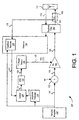
- FIG. 1 illustrates an embodiment of an RF transceiver 100 with an ET system.
- Transmit modulator 110 generates a digital transmit signal 101, which is upconverted by RF upconverter 102 to upconverted input signal 103 provided to the input of PA 104.
- PA 104 amplifies upconverted input signal 103 to generate amplified RF signal 105.
- the amplified RF signal 105 from PA 104 reaches antenna 112 as output signal 107 after passing through duplexer filter 106.
- Antenna 112 also receives a receive signal 113 which reaches receiver 114 after passing through duplexer filter 106.
- Duplexer filter 106 provides filtering between amplified RF signal 105 and a receive signal 113 received by antenna 112.
- Coupler 108 provides a feedback signal 115 to feedback receiver 116 that is representative of output signal 107.
- Digital transmit signal 101 is also provided to amplitude estimator 118 which estimates the amplitude of digital transmit signal 101.
- An estimated amplitude signal 119 is provided as an index to lookup table 120, which outputs signal 121 based on the estimated amplitude signal 119 and a feedback signal 117 from feedback receiver 116.
- Lookup table 120 may be populated with PA supply voltage values which are appropriate for various values of estimated transmit signal amplitude signal 119 and feedback signal 117, typically determined through PA characterization.
- Digital-to-analog converter (DAC) 122 converts the outputted PA supply voltage values from lookup table 120 to an analog signal 123, which controls ET power supply 124 to output specific voltages via supply voltage 125 to PA 104, so that PA 104 may operate with low headroom for good efficiency.
- a delay alignment circuit inserts a time delay at ET power supply 124 or within RF upconverter 102 to ensure proper time alignment between supply voltage 125 provided by ET power supply 124 and the amplified RF signal 105 at the output of PA 104.
- the values in lookup table 120 may be adjusted for a desired level of compression specified by feedback signal 117.
- Compression refers to the voltage operating headroom of PA 104.
- the desired compression levels are typically determined by PA and system characterization. For good efficiency, PA 104 may be operated with a high compression level, but the output signal from PA 104 should not exceed a level of acceptable distortion.
- the compression level should be lowered until the acceptable level of distortion is met.
- Adjacent channel power (ACP) is a common indicator of distortion in PAs.
- the feedback signal 117 may instead adjust a parameter of the amplitude estimator 118 to control compression. For example, the output of the amplitude estimator may be multiplied by the value x to increase compression when x is less than 1 and decrease compression when x is greater than 1.
- Feedback receiver 116 generates feedback signal 117 to control compression based on transmit signal 101 and coupled signal 115 received via coupler 108.
- Feedback receiver 116 either operates continuously during normal transmitter operation, periodically during transmitter operation, or operates during a calibration mode.
- Feedback receiver 116 downconverts coupled signal 115 to recover a downconverted baseband signal.
- Feedback receiver 116 evaluates the downconverted signal, and measures distortion in signal 115, representative of distortion in output signal 107. For example, in one embodiment, feedback receiver 116 calculates ACP by observing the power in the adjacent channel (for example, by performing a fast Fourier transform and taking the ratio of the power of the desired frequency channel of signal 115 to the power of the adjacent channels).
- feedback receiver 116 measures an error in the trajectory of coupled signal 115 as compared with the desired baseband transmit signal 101 as generated by transmit modulator 110, calculating the difference in these signals utilizing, for example, least-mean-squared techniques. Based on such distortion assessments, feedback receiver 116 provides feedback signal 117 to adjust the values in lookup table 120 to adjust the compression level just low enough to ensure distortion levels are acceptable.
- PA 104 may generate some noise outside the desired RF transmit band.
- the noise is generated due to a number of factors, including (a) AM-AM and AM-PM characteristics inherent in PA 104, (b) nonlinearities caused by operating PA 104 with low supply voltage headroom, (c) imperfections in the PA model for generating the variable power supply voltage, and (d) bandwidth limitations in the ET power supply 124.
- noise generated in the RF receive band can desensitize the RF receiver 114 of the transceiver to the receive signal 113.
- the radio system is often full duplex (the RF receiver 114 operates at the same time as the transmitter).
- noise generated by PA 104 can feed into receiver 114 during operation.
- Increased compression of PA 104 may increase noise in the receive band of receive signal 113.
- Duplexer filter 106 functions to limit this noise, but the filtering may be insufficient.
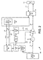
- FIG. 2 illustrates a second embodiment of a ET transceiver 200 in which parameters of the envelope tracking system are adjusted as a function of the tolerable noise in the receive path (receive noise margin), in order to limit the desensitization of the RF receiver 114.
- the system is similar to that of FIG. 1 , but includes a configuration block 254 and noise margin estimator 252, and omits some details previously described.
- the radio link quality is typically monitored in modern radio systems, e.g., by a noise margin estimator 252.
- the link quality may be assessed using parameters of the radio link such as receive signal strength, or bit or frame error rates.
- the noise margin estimator 252 can estimate the receive noise margin at the RF receiver 114 and can provide one or more feedback signals 251, 253 to a configuration block 254 that adjusts the parameters of the envelope tracking system accordingly.
- the receive noise margin will typically change dynamically, as radio conditions change. For example, many systems operate with high receive noise margins when the transmitter is used for high data rate transmission; the highest data rates will rarely be used in poor or marginal receive conditions. It is at these high data rates where the transmitter will operate at the highest power levels; thus substantial overall power savings are realized from an efficient PA. Under these conditions, the configuration block 254 adjusts the parameters of the ET system to maximize efficiency, while allowing higher than nominal receive band noise since the receive noise margin is high. Conversely, when radio conditions are poor, and the receive noise margin is low, the configuration block 254 adjusts the parameters of the ET system to minimize receive band noise, even at the expense of degraded PA efficiency.
- noise margin estimator 252 provides a receive signal strength indicator (RSSI) level 251 to configuration block 254 as an estimate of the receive noise margin.
- RSSI receive signal strength indicator
- configuration block 254 adjusts the parameters of the ET system to increase efficiency, even at the expense of receive band noise, since a high level of RSSI corresponds to a high receive noise margin at the RF receiver's input, and additional noise can be tolerated.
- configuration block 254 may adjust parameters in the lookup table 120 to increase compression, reduce filtering in the ET power supply 124 via control signal 257, and/or adjust biasing of the power amplifier via control signal 259. Effects of these adjustments on receive band noise and efficiency are described in further detail below.
- configuration block 254 adjusts the parameters of the ET system to decrease receive band noise, even at the expense of efficiency, since a low level of RSSI corresponds to a low receive noise margin at the RF receiver's input, and much additional noise cannot be tolerated.
- configuration block 254 may adjust parameters in the lookup table 120 to decrease compression, increase filtering in the ET power supply 124 via control signal 257, and/or adjust biasing of the power amplifier via control signal 259. Effects of these adjustments on receive band noise and efficiency are described in further detail below.
- the noise margin estimator 252 detects if the system is in the presence of a public safety network. This indication may be communicated to the radio through a cellular basestation. In this case, additional emissions and noise requirements may be imposed on the radio.
- the noise margin estimator 252 provides a public safety indicator (PSI) signal 253 to configuration block 254 which indicates to configuration block 254 that emissions and noise from PA 104 should be reduced. Configuration block 254 may adjust ET parameters in order to reduce emissions and noise, while trading off efficiency.
- PSI public safety indicator
- a different signal representative of the noise margin can be provided to the configuration block 254, such as, for example, a signal representing a bit or frame error rate, or a signal representing a combination of the above described factors.
- Configuration block 254 can adjust various parameters of the ET system based on the noise margin. For example, configuration block 254 may increase or reduce the compression of PA 104 via the lookup table 120 via feedback signal 255 to increase or decrease efficiency (with a corresponding increase or decrease in receive noise), as described earlier. Alternatively, the configuration block 254 may control compression by adjusting a parameter of the amplitude estimator 118 as described earlier.
- a less compressed PA sees its gain vary less with the supply voltage applied.
- errors in the path from lookup table 120 to supply voltage 125 which supplies PA 104 which normally cause noise and distortion when they erroneously vary the gain of PA 104, cause less noise and distortion when PA 104 is less compressed.
- PA 104 when PA 104 is less compressed, PA 104 operates with lower efficiency.
- a more compressed PA sees its gain vary more with the voltage applied.
- errors in the supply voltage for PA 104 cause more noise and distortion when PA 104 is more compressed.
- PA 104 operates with higher efficiency.
- Configuration block 254 may also adjust the filtering of the voltage control signal 123 in ET power supply 124 via filtering control signal 257.
- Filtering is used to limit the control bandwidth to envelope tracking power supply 124, which reduces noise because it prevents envelope tracking power supply 124 from attempting to generate rapid voltage changes to PA 104. Without the filtering, these rapid voltage changes are generated with inaccuracy due to inherent bandwidth limitations within the envelope tracking power supply 124, causing PA 104 to generate noise.
- configuration block 254 may command greater or less filtering of voltage control signal 123 when a low or high receive noise margin, respectively, is indicated.
- Configuration block 254 may also adjust the biasing of PA 104 via a bias control signal 259. Controlling the bias of PA 104 changes its AM/AM and AM/PM characteristics. Some AM/AM shapes can be more susceptible to the generation of noise, but also have higher efficiency.
- Configuration block 254 may also disable the dynamic ET system altogether, commanding envelope tracking power supply 124 to provide a static supply voltage to PA 104. This may be accomplished by adjusting lookup table 120 to provide the same PA supply voltage value regardless of transmit power. Alternatively, the PA supply voltage may be held constant during certain transmit periods, and changed between periods if the output power of PA 104 changes. Disabling the dynamic ET system in this way reduces noise associated with the envelope power supply 124, and can be commanded by configuration block 254 if a low receive noise margin is indicated.
Abstract
Description
- This application claims the benefit of
U.S. Provisional Patent Application No. 61/783,665 filed on March 14, 2013 - This disclosure relates generally to a radio frequency transceiver, and more specifically to an envelope tracking system in a radio frequency transceiver.
- Envelope Tracking (ET) systems are commonly utilized in the radio frequency (RF) transmitter section of a radio where power efficiency is important such as in cellular radios used in mobile phones. A typical ET system includes an RF power amplifier (PA) utilizing a variable power supply, which supplies the PA with a dynamically changing supply voltage that tracks the amplitude of the modulation. The goal of such an ET system is generally to improve efficiency by operating the PA with low headroom.
- Embodiments include an envelope tracking transceiver that adjusts envelope tracking parameters to achieve desired noise performance and power efficiency. In a first embodiment, an envelope tracking transceiver comprises a power amplifier, a lookup circuit, a power supply, a receiver, and a configuration circuit. The power amplifier receives an input signal and generates an amplified output signal. The power amplifier also receives a supply voltage providing power to the power amplifier. The lookup circuit generates a power supply control signal based on an estimated amplitude of the input signal and a feedback signal indicating a compression level for operating the power amplifier. The power supply provides the supply voltage to the power amplifier based on the power supply control signal. The receiver receives a receive signal and generates a noise margin signal representative of a noise margin of the receive signal. The configuration circuit generates the feedback signal based on the noise margin signal.
- In a second embodiment, the envelope tracking transceiver comprises a power amplifier, a lookup circuit, a power supply, a receiver, and a configuration circuit. The power amplifier receives an input signal and generates an amplified output signal. The power amplifier also receives a supply voltage providing power to the power amplifier. The lookup circuit generates a power supply control signal based on an estimated amplitude of the input signal. The power supply provides the supply voltage to the power amplifier based on the power supply control signal. The receiver receives a receive signal and generates a noise margin signal representative of a noise margin of the receive signal. The configuration circuit generates one or more control signals to control parameters of at least one of the power amplifier, the lookup circuit, and the power supply based on the noise margin signal.
- In a third embodiment, the envelope tracking transceiver comprises a power amplifier, a lookup circuit, a power supply, and a feedback receiver. The power amplifier receives an input signal and generates an amplified output signal. The power amplifier also receives a supply voltage providing power to the power amplifier. The lookup circuit generates a power supply control signal based on an estimated amplitude of the input signal and a feedback signal indicating a compression level for operating the power amplifier. The power supply provides the supply voltage to the power amplifier based on the power supply control signal. The feedback receiver generates a noise measure in the amplified output signal and generates the feedback signal responsive to the noise measure.
- The features and advantages described in the specification are not all inclusive and, in particular, many additional features and advantages will be apparent to one of ordinary skill in the art in view of the drawings and specification. Moreover, it should be noted that the language used in the specification has been principally selected for readability and instructional purposes, and may not have been selected to delineate or circumscribe the inventive subject matter.
- The teachings of the embodiments disclosed herein can be readily understood by considering the following detailed description in conjunction with the accompanying drawings.
-
FIG. 1 is a circuit diagram illustrating a first embodiment of an ET transceiver. -
FIG. 2 is a circuit diagram illustrating a second embodiment of an ET transceiver. - The Figures (FIG.) and the following description relate to various embodiments by way of illustration only. It should be noted that from the following discussion, alternative embodiments of the structures and methods disclosed herein will be readily recognized as viable alternatives that may be employed without departing from the principles discussed herein.
- Reference will now be made in detail to several embodiments, examples of which are illustrated in the accompanying figures. It is noted that wherever practicable similar or like reference numbers may be used in the figures and may indicate similar or like functionality. The figures depict various embodiments for purposes of illustration only. One skilled in the art will readily recognize from the following description that alternative embodiments of the structures and methods illustrated herein may be employed without departing from the principles described herein.
- An envelope tracking transceiver dynamically adjusts envelope tracking parameters to achieve the desired tradeoff between noise performance and power efficiency. Particularly, better power efficiency of the transmitter can be obtained by sacrificing noise performance of the transmitted and received signals of the transceiver. When higher levels of noise are acceptable, the envelope tracking transceiver dynamically adjusts transmitter parameters to achieve better power efficiency while sacrificing noise performance. When lower levels of noise are desired, the envelope tracking transceiver dynamically adjusts parameters to achieve better noise performance while sacrificing efficiency.
-
FIG. 1 illustrates an embodiment of anRF transceiver 100 with an ET system.Transmit modulator 110 generates adigital transmit signal 101, which is upconverted byRF upconverter 102 toupconverted input signal 103 provided to the input ofPA 104. PA 104 amplifiesupconverted input signal 103 to generate amplifiedRF signal 105. The amplifiedRF signal 105 fromPA 104 reachesantenna 112 asoutput signal 107 after passing throughduplexer filter 106.Antenna 112 also receives areceive signal 113 which reachesreceiver 114 after passing throughduplexer filter 106.Duplexer filter 106 provides filtering between amplifiedRF signal 105 and a receivesignal 113 received byantenna 112.Coupler 108 provides afeedback signal 115 tofeedback receiver 116 that is representative ofoutput signal 107. -
Digital transmit signal 101 is also provided toamplitude estimator 118 which estimates the amplitude ofdigital transmit signal 101. For example, in one embodiment,amplitude estimator 118 estimates the amplitude based on the equation Amplitude= sqrt(I2 + Q2), where I and Q are the inphase and quadrature components respectively of thedigital transmit signal 101. An estimatedamplitude signal 119 is provided as an index to lookup table 120, which outputssignal 121 based on the estimatedamplitude signal 119 and afeedback signal 117 fromfeedback receiver 116. Lookup table 120 may be populated with PA supply voltage values which are appropriate for various values of estimated transmitsignal amplitude signal 119 andfeedback signal 117, typically determined through PA characterization. - Digital-to-analog converter (DAC) 122 converts the outputted PA supply voltage values from lookup table 120 to an
analog signal 123, which controlsET power supply 124 to output specific voltages viasupply voltage 125 toPA 104, so thatPA 104 may operate with low headroom for good efficiency. In one embodiment, a delay alignment circuit (not shown) inserts a time delay atET power supply 124 or withinRF upconverter 102 to ensure proper time alignment betweensupply voltage 125 provided byET power supply 124 and the amplifiedRF signal 105 at the output ofPA 104. - The values in lookup table 120 may be adjusted for a desired level of compression specified by
feedback signal 117. Compression refers to the voltage operating headroom ofPA 104. For example, in one embodiment, values in lookup table 120 are adjusted by multiplying values in lookup table 120 by a value x. Compression increases when x is less than 1 and decreases when x is greater than 1. For example, if x=0.9, thesupply voltage 125 supplied toPA 104 is effectively decreased by 10%. If x=1.1, thesupply voltage 125 supplied toPA 104 is effectively increased by 10%. The desired compression levels are typically determined by PA and system characterization. For good efficiency,PA 104 may be operated with a high compression level, but the output signal fromPA 104 should not exceed a level of acceptable distortion. Otherwise, if the acceptable level of distortion is exceeded, the compression level should be lowered until the acceptable level of distortion is met. Adjacent channel power (ACP) is a common indicator of distortion in PAs. Alternatively, instead offeedback signal 117 adjusting values in the lookup table 120, thefeedback signal 117 may instead adjust a parameter of theamplitude estimator 118 to control compression. For example, the output of the amplitude estimator may be multiplied by the value x to increase compression when x is less than 1 and decrease compression when x is greater than 1. -
Feedback receiver 116 generatesfeedback signal 117 to control compression based on transmitsignal 101 and coupled signal 115 received viacoupler 108.Feedback receiver 116 either operates continuously during normal transmitter operation, periodically during transmitter operation, or operates during a calibration mode.Feedback receiver 116 downconverts coupled signal 115 to recover a downconverted baseband signal.Feedback receiver 116 evaluates the downconverted signal, and measures distortion insignal 115, representative of distortion inoutput signal 107. For example, in one embodiment,feedback receiver 116 calculates ACP by observing the power in the adjacent channel (for example, by performing a fast Fourier transform and taking the ratio of the power of the desired frequency channel ofsignal 115 to the power of the adjacent channels). In one embodiment,feedback receiver 116 measures an error in the trajectory of coupledsignal 115 as compared with the desired baseband transmitsignal 101 as generated by transmitmodulator 110, calculating the difference in these signals utilizing, for example, least-mean-squared techniques. Based on such distortion assessments,feedback receiver 116 providesfeedback signal 117 to adjust the values in lookup table 120 to adjust the compression level just low enough to ensure distortion levels are acceptable. - In ET systems such as the
transceiver 100 ofFIG. 1 ,PA 104 may generate some noise outside the desired RF transmit band. The noise is generated due to a number of factors, including (a) AM-AM and AM-PM characteristics inherent inPA 104, (b) nonlinearities caused by operatingPA 104 with low supply voltage headroom, (c) imperfections in the PA model for generating the variable power supply voltage, and (d) bandwidth limitations in theET power supply 124. - In particular, noise generated in the RF receive band can desensitize the
RF receiver 114 of the transceiver to the receivesignal 113. In cellular radios used in mobile phones, the radio system is often full duplex (theRF receiver 114 operates at the same time as the transmitter). Thus, noise generated byPA 104 can feed intoreceiver 114 during operation. Increased compression ofPA 104 may increase noise in the receive band of receivesignal 113.Duplexer filter 106 functions to limit this noise, but the filtering may be insufficient. -
FIG. 2 illustrates a second embodiment of aET transceiver 200 in which parameters of the envelope tracking system are adjusted as a function of the tolerable noise in the receive path (receive noise margin), in order to limit the desensitization of theRF receiver 114. The system is similar to that ofFIG. 1 , but includes aconfiguration block 254 andnoise margin estimator 252, and omits some details previously described. - The radio link quality is typically monitored in modern radio systems, e.g., by a
noise margin estimator 252. The link quality may be assessed using parameters of the radio link such as receive signal strength, or bit or frame error rates. Thus, thenoise margin estimator 252 can estimate the receive noise margin at theRF receiver 114 and can provide one or more feedback signals 251, 253 to aconfiguration block 254 that adjusts the parameters of the envelope tracking system accordingly. - The receive noise margin will typically change dynamically, as radio conditions change. For example, many systems operate with high receive noise margins when the transmitter is used for high data rate transmission; the highest data rates will rarely be used in poor or marginal receive conditions. It is at these high data rates where the transmitter will operate at the highest power levels; thus substantial overall power savings are realized from an efficient PA. Under these conditions, the
configuration block 254 adjusts the parameters of the ET system to maximize efficiency, while allowing higher than nominal receive band noise since the receive noise margin is high. Conversely, when radio conditions are poor, and the receive noise margin is low, theconfiguration block 254 adjusts the parameters of the ET system to minimize receive band noise, even at the expense of degraded PA efficiency. - In one embodiment,
noise margin estimator 252 provides a receive signal strength indicator (RSSI)level 251 to configuration block 254 as an estimate of the receive noise margin. When a high level of RSSI is detected via signal 251 (e.g., above a threshold noise margin),configuration block 254 adjusts the parameters of the ET system to increase efficiency, even at the expense of receive band noise, since a high level of RSSI corresponds to a high receive noise margin at the RF receiver's input, and additional noise can be tolerated. For example, in one embodiment,configuration block 254 may adjust parameters in the lookup table 120 to increase compression, reduce filtering in theET power supply 124 viacontrol signal 257, and/or adjust biasing of the power amplifier viacontrol signal 259. Effects of these adjustments on receive band noise and efficiency are described in further detail below. - Conversely, if a low level of RSSI is detected via signal 251 (e.g., below the threshold noise margin),
configuration block 254 adjusts the parameters of the ET system to decrease receive band noise, even at the expense of efficiency, since a low level of RSSI corresponds to a low receive noise margin at the RF receiver's input, and much additional noise cannot be tolerated. For example, in one embodiment,configuration block 254 may adjust parameters in the lookup table 120 to decrease compression, increase filtering in theET power supply 124 viacontrol signal 257, and/or adjust biasing of the power amplifier viacontrol signal 259. Effects of these adjustments on receive band noise and efficiency are described in further detail below. - In another embodiment, the
noise margin estimator 252 detects if the system is in the presence of a public safety network. This indication may be communicated to the radio through a cellular basestation. In this case, additional emissions and noise requirements may be imposed on the radio. In one embodiment, thenoise margin estimator 252 provides a public safety indicator (PSI) signal 253 to configuration block 254 which indicates to configuration block 254 that emissions and noise fromPA 104 should be reduced.Configuration block 254 may adjust ET parameters in order to reduce emissions and noise, while trading off efficiency. - In yet other embodiments, a different signal representative of the noise margin can be provided to the
configuration block 254, such as, for example, a signal representing a bit or frame error rate, or a signal representing a combination of the above described factors. -
Configuration block 254 can adjust various parameters of the ET system based on the noise margin. For example,configuration block 254 may increase or reduce the compression ofPA 104 via the lookup table 120 viafeedback signal 255 to increase or decrease efficiency (with a corresponding increase or decrease in receive noise), as described earlier. Alternatively, theconfiguration block 254 may control compression by adjusting a parameter of theamplitude estimator 118 as described earlier. - A less compressed PA sees its gain vary less with the supply voltage applied. Thus, errors in the path from lookup table 120 to supply
voltage 125 which suppliesPA 104, which normally cause noise and distortion when they erroneously vary the gain ofPA 104, cause less noise and distortion whenPA 104 is less compressed. However, whenPA 104 is less compressed,PA 104 operates with lower efficiency. Conversely, a more compressed PA sees its gain vary more with the voltage applied. Thus, errors in the supply voltage forPA 104 cause more noise and distortion whenPA 104 is more compressed. However, whenPA 104 is more compressed,PA 104 operates with higher efficiency. -
Configuration block 254 may also adjust the filtering of thevoltage control signal 123 inET power supply 124 viafiltering control signal 257. Filtering is used to limit the control bandwidth to envelope trackingpower supply 124, which reduces noise because it prevents envelope trackingpower supply 124 from attempting to generate rapid voltage changes toPA 104. Without the filtering, these rapid voltage changes are generated with inaccuracy due to inherent bandwidth limitations within the envelope trackingpower supply 124, causingPA 104 to generate noise. However, reducing filtering allows envelope trackingpower supply 124 to achieve lower supply voltages toPA 104, increasing efficiency. Thus,configuration block 254 may command greater or less filtering ofvoltage control signal 123 when a low or high receive noise margin, respectively, is indicated. -
Configuration block 254 may also adjust the biasing ofPA 104 via abias control signal 259. Controlling the bias ofPA 104 changes its AM/AM and AM/PM characteristics. Some AM/AM shapes can be more susceptible to the generation of noise, but also have higher efficiency. -
Configuration block 254 may also disable the dynamic ET system altogether, commanding envelope trackingpower supply 124 to provide a static supply voltage toPA 104. This may be accomplished by adjusting lookup table 120 to provide the same PA supply voltage value regardless of transmit power. Alternatively, the PA supply voltage may be held constant during certain transmit periods, and changed between periods if the output power ofPA 104 changes. Disabling the dynamic ET system in this way reduces noise associated with theenvelope power supply 124, and can be commanded byconfiguration block 254 if a low receive noise margin is indicated. - Upon reading this disclosure, those of skill in the art will appreciate still additional alternative designs for an envelope tracking system with adjustment for noise. Thus, while particular embodiments and applications have been illustrated and described, it is to be understood that the embodiments discussed herein are not limited to the precise construction and components disclosed herein and that various modifications, changes and variations which will be apparent to those skilled in the art may be made in the arrangement, operation and details of the method and apparatus disclosed herein without departing from the scope of the disclosure.
Claims (15)
- An envelope tracking transceiver (100) comprising:a power amplifier (104) configured to receive an upconverted input signal (103) and generate an amplified output signal (105), the power amplifier (104) receiving a supply voltage (125) providing power to the power amplifier (104);a lookup circuit (120) configured to generate a power supply control signal (121) based on an estimated amplitude (119) of an input signal (101) that is upconverted to the upconverted input signal (103) and a feedback signal (117) indicating an amount of voltage headroom for operating the power amplifier (104);a power supply (124) configured to provide the supply voltage (125) to the power amplifier (104) based on the power supply control signal (121); anda feedback receiver (116) configured to generate a noise measure in the amplified output signal (105) and to generate the feedback signal (117) responsive to the noise measure.
- The envelope tracking transceiver (100) of claim 1 wherein the feedback receiver (116) is further configured to determine the noise measure based on the input signal (101) and a signal (115) representative of the amplified output signal (105).
- The envelope tracking transceiver (100) of claim 2 wherein the feedback receiver (116) is further configured to downsample the signal (115) representative of the amplified output signal (105) and perform a comparison between the downsampled signal and the input signal (101).
- The envelope tracking transceiver (100) of claim 1 wherein the feedback signal (117) decreases the amount of voltage headroom responsive to the noise measure falling below a threshold.
- The envelope tracking transceiver (100) of claim 4 wherein the feedback signal (117) increases the amount of voltage headroom responsive to the noise measure exceeding the threshold.
- The envelope tracking transceiver (100) of claim 1 further comprising a digital-to-analog converter (122) configured to receive the power supply control signal (121) and generate an analog signal (123) based on the power supply control signal (121).
- The envelope tracking transceiver (100) of claim 6 wherein the power supply (124) is further configured to provide the supply voltage (125) to the power amplifier (104) based on the analog signal (123).
- The envelope tracking transceiver (100) of any one of claims 1 to 7 further comprising an amplitude estimator (118) configured to receive the input signal (101) and generate the estimated amplitude (119).
- The envelope tracking transceiver (100) of any one of claims 1 to 8 further comprising an upconverter (102) configured to receive the input signal (101) and generate the upconverted input signal (103).
- The envelope tracking transceiver (100) of any one of claims 1 to 9 further comprising a transmit modulator (110) configured to generate the input signal (101).
- The envelope tracking transceiver (100) of any one of claims 1 to 10 wherein the feedback receiver (116) is further configured to generate the noise measure while the envelope tracking transceiver (100) is operating in at least one of a transmit mode of operation and a calibration mode of operation.
- The envelope tracking transceiver (100) of any one of claims 1 to 11 wherein the noise measure represents an adjacent channel power.
- The envelope tracking transceiver (100) of any one of claims 1 to 12 further comprising a duplex filter (106) coupled between an output of the power amplifier (104) and an antenna (112).
- The envelope tracking transceiver (100) of any one of claims 1 to 12 further comprising a coupler (108) coupled between an output of the power amplifier (104) and an antenna (112), the coupler (108) being configured to generate a coupled signal (115).
- The envelope tracking transceiver (100) of claim 14 wherein the feedback receiver (116) is further configured to generate the noise measure based on the input signal (101) and the coupled signal (115).
Applications Claiming Priority (2)
| Application Number | Priority Date | Filing Date | Title |
|---|---|---|---|
| US201361783665P | 2013-03-14 | 2013-03-14 | |
| EP14776359.3A EP2974005B1 (en) | 2013-03-14 | 2014-03-12 | Et system with adjustment for noise |
Related Parent Applications (2)
| Application Number | Title | Priority Date | Filing Date |
|---|---|---|---|
| EP14776359.3A Division-Into EP2974005B1 (en) | 2013-03-14 | 2014-03-12 | Et system with adjustment for noise |
| EP14776359.3A Division EP2974005B1 (en) | 2013-03-14 | 2014-03-12 | Et system with adjustment for noise |
Publications (3)
| Publication Number | Publication Date |
|---|---|
| EP3089371A2 true EP3089371A2 (en) | 2016-11-02 |
| EP3089371A3 EP3089371A3 (en) | 2017-01-04 |
| EP3089371B1 EP3089371B1 (en) | 2017-10-18 |
Family
ID=51529462
Family Applications (2)
| Application Number | Title | Priority Date | Filing Date |
|---|---|---|---|
| EP14776359.3A Active EP2974005B1 (en) | 2013-03-14 | 2014-03-12 | Et system with adjustment for noise |
| EP16175782.8A Active EP3089371B1 (en) | 2013-03-14 | 2014-03-12 | Et system with adjustment for noise |
Family Applications Before (1)
| Application Number | Title | Priority Date | Filing Date |
|---|---|---|---|
| EP14776359.3A Active EP2974005B1 (en) | 2013-03-14 | 2014-03-12 | Et system with adjustment for noise |
Country Status (7)
| Country | Link |
|---|---|
| US (2) | US9271236B2 (en) |
| EP (2) | EP2974005B1 (en) |
| JP (2) | JP6178489B2 (en) |
| KR (1) | KR102179318B1 (en) |
| CN (1) | CN105027429B (en) |
| HK (1) | HK1211751A1 (en) |
| WO (1) | WO2014159753A1 (en) |
Families Citing this family (41)
| Publication number | Priority date | Publication date | Assignee | Title |
|---|---|---|---|---|
| US8718579B2 (en) | 2012-03-04 | 2014-05-06 | Quantance, Inc. | Envelope tracking power amplifier system with delay calibration |
| EP2974005B1 (en) | 2013-03-14 | 2018-06-20 | Quantance, Inc. | Et system with adjustment for noise |
| KR102174242B1 (en) | 2013-03-15 | 2020-11-04 | 퀀탄스, 인코포레이티드 | Envelope tracking system with internal power amplifier characterization |
| US10333474B2 (en) * | 2014-05-19 | 2019-06-25 | Skyworks Solutions, Inc. | RF transceiver front end module with improved linearity |
| US10554377B2 (en) * | 2014-08-28 | 2020-02-04 | Toyota Infotechnology Center Usa, Inc. | Full-duplex coordination system |
| US9800274B2 (en) * | 2015-07-03 | 2017-10-24 | Mediatek, Inc. | Communication units and methods for power supply control |
| US10250194B2 (en) | 2015-11-13 | 2019-04-02 | Analog Devices Global | Broadband envelope tracking |
| US10128798B2 (en) | 2016-07-29 | 2018-11-13 | Qualcomm Incorporated | Adjusting envelope tracking power supply |
| US10374557B2 (en) * | 2016-10-28 | 2019-08-06 | Samsung Electro-Mechanics Co., Ltd. | Adaptive multiband power amplifier apparatus |
| US10158330B1 (en) | 2017-07-17 | 2018-12-18 | Qorvo Us, Inc. | Multi-mode envelope tracking amplifier circuit |
| US10944365B2 (en) | 2018-06-28 | 2021-03-09 | Qorvo Us, Inc. | Envelope tracking amplifier circuit |
| US11088618B2 (en) | 2018-09-05 | 2021-08-10 | Qorvo Us, Inc. | PWM DC-DC converter with linear voltage regulator for DC assist |
| US10911001B2 (en) | 2018-10-02 | 2021-02-02 | Qorvo Us, Inc. | Envelope tracking amplifier circuit |
| US10985702B2 (en) | 2018-10-31 | 2021-04-20 | Qorvo Us, Inc. | Envelope tracking system |
| US10938351B2 (en) | 2018-10-31 | 2021-03-02 | Qorvo Us, Inc. | Envelope tracking system |
| US11018638B2 (en) | 2018-10-31 | 2021-05-25 | Qorvo Us, Inc. | Multimode envelope tracking circuit and related apparatus |
| CN111200430B (en) * | 2018-11-19 | 2023-01-13 | 马克西姆综合产品公司 | Driver circuit system and related method thereof |
| US11031909B2 (en) | 2018-12-04 | 2021-06-08 | Qorvo Us, Inc. | Group delay optimization circuit and related apparatus |
| US11082007B2 (en) | 2018-12-19 | 2021-08-03 | Qorvo Us, Inc. | Envelope tracking integrated circuit and related apparatus |
| US11146213B2 (en) | 2019-01-15 | 2021-10-12 | Qorvo Us, Inc. | Multi-radio access technology envelope tracking amplifier apparatus |
| US11025458B2 (en) | 2019-02-07 | 2021-06-01 | Qorvo Us, Inc. | Adaptive frequency equalizer for wide modulation bandwidth envelope tracking |
| US10998859B2 (en) * | 2019-02-07 | 2021-05-04 | Qorvo Us, Inc. | Dual-input envelope tracking integrated circuit and related apparatus |
| US11233481B2 (en) | 2019-02-18 | 2022-01-25 | Qorvo Us, Inc. | Modulated power apparatus |
| US11374482B2 (en) | 2019-04-02 | 2022-06-28 | Qorvo Us, Inc. | Dual-modulation power management circuit |
| US11082009B2 (en) | 2019-04-12 | 2021-08-03 | Qorvo Us, Inc. | Envelope tracking power amplifier apparatus |
| US11018627B2 (en) | 2019-04-17 | 2021-05-25 | Qorvo Us, Inc. | Multi-bandwidth envelope tracking integrated circuit and related apparatus |
| US11424719B2 (en) | 2019-04-18 | 2022-08-23 | Qorvo Us, Inc. | Multi-bandwidth envelope tracking integrated circuit |
| US11031911B2 (en) | 2019-05-02 | 2021-06-08 | Qorvo Us, Inc. | Envelope tracking integrated circuit and related apparatus |
| US11349436B2 (en) | 2019-05-30 | 2022-05-31 | Qorvo Us, Inc. | Envelope tracking integrated circuit |
| CN110198173A (en) * | 2019-05-31 | 2019-09-03 | 努比亚技术有限公司 | A kind of adjusting method of mobile terminal, radio circuit, mobile terminal and storage medium |
| US11539289B2 (en) | 2019-08-02 | 2022-12-27 | Qorvo Us, Inc. | Multi-level charge pump circuit |
| US11309922B2 (en) | 2019-12-13 | 2022-04-19 | Qorvo Us, Inc. | Multi-mode power management integrated circuit in a small formfactor wireless apparatus |
| CN111064478B (en) * | 2019-12-16 | 2021-04-27 | 紫光展讯通信(惠州)有限公司 | Time delay calibration method, wireless radio frequency device and computer readable storage medium |
| US11349513B2 (en) | 2019-12-20 | 2022-05-31 | Qorvo Us, Inc. | Envelope tracking system |
| US11539330B2 (en) | 2020-01-17 | 2022-12-27 | Qorvo Us, Inc. | Envelope tracking integrated circuit supporting multiple types of power amplifiers |
| US11716057B2 (en) | 2020-01-28 | 2023-08-01 | Qorvo Us, Inc. | Envelope tracking circuitry |
| US11728774B2 (en) | 2020-02-26 | 2023-08-15 | Qorvo Us, Inc. | Average power tracking power management integrated circuit |
| US11196392B2 (en) | 2020-03-30 | 2021-12-07 | Qorvo Us, Inc. | Device and device protection system |
| US11588449B2 (en) | 2020-09-25 | 2023-02-21 | Qorvo Us, Inc. | Envelope tracking power amplifier apparatus |
| US11728796B2 (en) | 2020-10-14 | 2023-08-15 | Qorvo Us, Inc. | Inverted group delay circuit |
| US11909385B2 (en) | 2020-10-19 | 2024-02-20 | Qorvo Us, Inc. | Fast-switching power management circuit and related apparatus |
Family Cites Families (58)
| Publication number | Priority date | Publication date | Assignee | Title |
|---|---|---|---|---|
| JPH0644716B2 (en) | 1984-08-14 | 1994-06-08 | 日本電気株式会社 | Wireless communication device |
| JPH10209770A (en) * | 1997-01-27 | 1998-08-07 | Toshiba Corp | Power amplifier and radio telephone device using the same power amplifier |
| US6148220A (en) * | 1997-04-25 | 2000-11-14 | Triquint Semiconductor, Inc. | Battery life extending technique for mobile wireless applications |
| US6084468A (en) | 1997-10-06 | 2000-07-04 | Motorola, Inc. | Method and apparatus for high efficiency wideband power amplification |
| US6130910A (en) | 1997-11-03 | 2000-10-10 | Motorola, Inc. | Method and apparatus for high efficiency wideband power amplification |
| US6191653B1 (en) * | 1998-11-18 | 2001-02-20 | Ericsson Inc. | Circuit and method for linearizing amplitude modulation in a power amplifier |
| US6356146B1 (en) | 1999-07-13 | 2002-03-12 | Pmc-Sierra, Inc. | Amplifier measurement and modeling processes for use in generating predistortion parameters |
| GB2370435A (en) | 2000-12-22 | 2002-06-26 | Nokia Mobile Phones Ltd | A polar loop transmitter for a mobile phone |
| AUPR438601A0 (en) * | 2001-04-11 | 2001-05-17 | Cochlear Limited | Variable sensitivity control for a cochlear implant |
| US6683496B2 (en) | 2001-08-20 | 2004-01-27 | Harris Corporation | System and method for minimizing dissipation in RF power amplifiers |
| US6784744B2 (en) | 2001-09-27 | 2004-08-31 | Powerq Technologies, Inc. | Amplifier circuits and methods |
| US7551688B2 (en) | 2002-04-18 | 2009-06-23 | Nokia Corporation | Waveforms for envelope tracking transmitter |
| US6646501B1 (en) | 2002-06-25 | 2003-11-11 | Nortel Networks Limited | Power amplifier configuration |
| US7263135B2 (en) | 2002-10-03 | 2007-08-28 | Matsushita Electric Industrial Co., Ltd. | Transmitting method and transmitter apparatus |
| CN100581052C (en) | 2004-08-13 | 2010-01-13 | 深圳赛意法微电子有限公司 | Automatic gain control system with self-adaptive climb and decay time |
| US7190221B2 (en) | 2004-10-22 | 2007-03-13 | Nokia Corporation | Method and apparatus for maintaining constant linearity for a power amplifier over varying load conditions |
| US7348842B2 (en) * | 2005-01-19 | 2008-03-25 | Micro-Mobio | Multi-substrate RF module for wireless communication devices |
| US20070066224A1 (en) | 2005-02-28 | 2007-03-22 | Sirit, Inc. | High efficiency RF amplifier and envelope modulator |
| US20060199553A1 (en) | 2005-03-07 | 2006-09-07 | Andrew Corporation | Integrated transceiver with envelope tracking |
| US7418032B2 (en) | 2005-03-15 | 2008-08-26 | International Business Machines Corporation | Altering power consumption in communication links based on measured noise |
| WO2006114792A1 (en) | 2005-04-27 | 2006-11-02 | Paragon Communications Ltd. | Transformer-capacitor enhancement circuitry for power amplifiers |
| US7761066B2 (en) | 2006-01-27 | 2010-07-20 | Marvell World Trade Ltd. | Variable power adaptive transmitter |
| US8032097B2 (en) | 2006-02-03 | 2011-10-04 | Quantance, Inc. | Amplitude error de-glitching circuit and method of operating |
| US7522676B2 (en) | 2006-02-06 | 2009-04-21 | Nokia Corporation | Method and system for transmitter envelope delay calibration |
| JP2008283678A (en) | 2007-04-11 | 2008-11-20 | Panasonic Corp | Transmission circuit and communication device |
| US7466195B2 (en) | 2007-05-18 | 2008-12-16 | Quantance, Inc. | Error driven RF power amplifier control with increased efficiency |
| US20090004981A1 (en) | 2007-06-27 | 2009-01-01 | Texas Instruments Incorporated | High efficiency digital transmitter incorporating switching power supply and linear power amplifier |
| US8463189B2 (en) | 2007-07-31 | 2013-06-11 | Texas Instruments Incorporated | Predistortion calibration and built in self testing of a radio frequency power amplifier using subharmonic mixing |
| US7783269B2 (en) | 2007-09-20 | 2010-08-24 | Quantance, Inc. | Power amplifier controller with polar transmitter |
| US8014735B2 (en) * | 2007-11-06 | 2011-09-06 | Quantance, Inc. | RF power amplifier controlled by estimated distortion level of output signal of power amplifier |
| GB0725110D0 (en) | 2007-12-21 | 2008-01-30 | Wolfson Microelectronics Plc | Gain control based on noise level |
| US8620233B2 (en) * | 2008-04-11 | 2013-12-31 | Samsung Electroncs Co., Ltd. | Method of power amplifier predistortion adaptation using compression detection |
| US8072205B1 (en) * | 2008-04-29 | 2011-12-06 | Analog Devices, Inc. | Peak-to-average measurement with envelope pre-detection |
| US8018277B2 (en) * | 2008-09-09 | 2011-09-13 | Quantance, Inc. | RF power amplifier system with impedance modulation |
| US8331883B2 (en) | 2008-10-30 | 2012-12-11 | Apple Inc. | Electronic devices with calibrated radio frequency communications circuitry |
| US8064852B2 (en) | 2008-11-13 | 2011-11-22 | Panasonic Corporation | Methods and apparatus for dynamically compensating for DC offset drift and other PVT-related signal variations in polar transmitters |
| WO2010064091A1 (en) * | 2008-12-03 | 2010-06-10 | Freescale Semiconductor, Inc. | Operating parameter control for a power amplifier |
| JP5212316B2 (en) * | 2009-09-03 | 2013-06-19 | 富士通株式会社 | Wireless communication apparatus and wireless communication method |
| US8744009B2 (en) * | 2009-09-25 | 2014-06-03 | General Dynamics C4 Systems, Inc. | Reducing transmitter-to-receiver non-linear distortion at a transmitter prior to estimating and cancelling known non-linear distortion at a receiver |
| US8731496B2 (en) | 2009-12-18 | 2014-05-20 | Quantance, Inc. | Power amplifier power controller |
| US8183917B2 (en) * | 2010-06-04 | 2012-05-22 | Quantance, Inc. | RF power amplifier circuit with mismatch tolerance |
| CN102340283B (en) * | 2010-07-14 | 2014-05-28 | 大唐移动通信设备有限公司 | Method and device for envelope tracking |
| CN102075149B (en) * | 2010-12-03 | 2013-01-23 | 哈尔滨工业大学深圳研究生院 | Power envelope tracing power supply of multi-phase interleaving radio-frequency power amplifier |
| KR101982956B1 (en) | 2011-02-07 | 2019-05-27 | 스카이워크스 솔루션즈, 인코포레이티드 | Methods of calibrating a power amplifier system to compensate for envelope amplitude misalignment |
| GB2489002A (en) * | 2011-03-14 | 2012-09-19 | Nujira Ltd | Delay adjustment to reduce distortion in an envelope tracking transmitter |
| GB2489497A (en) | 2011-03-31 | 2012-10-03 | Nujira Ltd | Matching the properties of the envelope path to the properties of the main signal path in an envelope tracking amplifier |
| US8718188B2 (en) * | 2011-04-25 | 2014-05-06 | Skyworks Solutions, Inc. | Apparatus and methods for envelope tracking |
| US9066368B2 (en) | 2011-06-08 | 2015-06-23 | Broadcom Corporation | Method of calibrating the delay of an envelope tracking signal |
| US9083453B2 (en) | 2011-06-23 | 2015-07-14 | Qualcomm Incorporated | Power supply generator with noise cancellation |
| US8754706B2 (en) | 2011-08-02 | 2014-06-17 | Qualcomm Incorporated | Power based feedback for improved power amplifier (PA) efficiency |
| US20130076418A1 (en) | 2011-09-27 | 2013-03-28 | Intel Mobile Communications GmbH | System and Method for Calibration of Timing Mismatch for Envelope Tracking Transmit Systems |
| US8880012B2 (en) * | 2012-01-19 | 2014-11-04 | Motorola Mobility Llc | Method and apparatus for resource block based transmitter optimization in wireless communication devices |
| JP5624569B2 (en) | 2012-02-17 | 2014-11-12 | 株式会社東芝 | Power amplifier |
| US8718579B2 (en) | 2012-03-04 | 2014-05-06 | Quantance, Inc. | Envelope tracking power amplifier system with delay calibration |
| US20140241462A1 (en) * | 2013-02-26 | 2014-08-28 | Nvidia Corporation | Circuit and method for envelope tracking and envelope-tracking transmitter for radio-frequency transmission |
| EP2974005B1 (en) | 2013-03-14 | 2018-06-20 | Quantance, Inc. | Et system with adjustment for noise |
| KR102174242B1 (en) | 2013-03-15 | 2020-11-04 | 퀀탄스, 인코포레이티드 | Envelope tracking system with internal power amplifier characterization |
| GB2519361B (en) | 2013-10-21 | 2015-09-16 | Nujira Ltd | Reduced bandwidth of signal in an envelope path for envelope tracking system |
-
2014
- 2014-03-12 EP EP14776359.3A patent/EP2974005B1/en active Active
- 2014-03-12 EP EP16175782.8A patent/EP3089371B1/en active Active
- 2014-03-12 US US14/207,296 patent/US9271236B2/en active Active
- 2014-03-12 KR KR1020157024836A patent/KR102179318B1/en active IP Right Grant
- 2014-03-12 WO PCT/US2014/024999 patent/WO2014159753A1/en active Application Filing
- 2014-03-12 CN CN201480013417.XA patent/CN105027429B/en active Active
- 2014-03-12 JP JP2016501714A patent/JP6178489B2/en active Active
-
2015
- 2015-12-11 HK HK15112232.6A patent/HK1211751A1/en unknown
-
2016
- 2016-02-17 US US15/045,659 patent/US9794884B2/en active Active
-
2017
- 2017-07-13 JP JP2017136976A patent/JP6247787B1/en active Active
Non-Patent Citations (1)
| Title |
|---|
| None |
Also Published As
| Publication number | Publication date |
|---|---|
| JP6247787B1 (en) | 2017-12-13 |
| KR20150129730A (en) | 2015-11-20 |
| EP2974005A1 (en) | 2016-01-20 |
| CN105027429A (en) | 2015-11-04 |
| EP2974005B1 (en) | 2018-06-20 |
| KR102179318B1 (en) | 2020-11-16 |
| JP2017225133A (en) | 2017-12-21 |
| CN105027429B (en) | 2018-03-30 |
| US9794884B2 (en) | 2017-10-17 |
| HK1211751A1 (en) | 2016-05-27 |
| US9271236B2 (en) | 2016-02-23 |
| EP3089371B1 (en) | 2017-10-18 |
| EP3089371A3 (en) | 2017-01-04 |
| EP2974005A4 (en) | 2016-06-08 |
| US20140274227A1 (en) | 2014-09-18 |
| WO2014159753A1 (en) | 2014-10-02 |
| JP6178489B2 (en) | 2017-08-09 |
| JP2016516353A (en) | 2016-06-02 |
| US20160165543A1 (en) | 2016-06-09 |
Similar Documents
| Publication | Publication Date | Title |
|---|---|---|
| US9794884B2 (en) | Envelope tracking system with adjustment for noise | |
| EP2974006B1 (en) | Envelope tracking system with internal power amplifier characterization | |
| US7741903B2 (en) | Distortion-driven power amplifier power supply controller | |
| US8014735B2 (en) | RF power amplifier controlled by estimated distortion level of output signal of power amplifier | |
| US8400217B2 (en) | RF power amplifier circuit with mismatch tolerance | |
| US8022761B2 (en) | Error driven RF power amplifier control with increased efficiency | |
| EP2296269B1 (en) | Power amplifier controller circuit | |
| EP2342779B1 (en) | Rf power amplifier system with impedance modulation | |
| US20130229228A1 (en) | Noise Optimized Envelope Tracking System for Power Amplifiers | |
| EP2779555B1 (en) | Method and apparatus for adjusting predistortion coefficients | |
| EP1861921B1 (en) | A method to track analog gain step magnitudes online during operation of wireless mobile devices | |
| US9853608B2 (en) | Temperature compensation technique for envelope tracking system |
Legal Events
| Date | Code | Title | Description |
|---|---|---|---|
| PUAI | Public reference made under article 153(3) epc to a published international application that has entered the european phase |
Free format text: ORIGINAL CODE: 0009012 |
|
| AC | Divisional application: reference to earlier application |
Ref document number: 2974005 Country of ref document: EP Kind code of ref document: P |
|
| AK | Designated contracting states |
Kind code of ref document: A2 Designated state(s): AL AT BE BG CH CY CZ DE DK EE ES FI FR GB GR HR HU IE IS IT LI LT LU LV MC MK MT NL NO PL PT RO RS SE SI SK SM TR |
|
| PUAL | Search report despatched |
Free format text: ORIGINAL CODE: 0009013 |
|
| AK | Designated contracting states |
Kind code of ref document: A3 Designated state(s): AL AT BE BG CH CY CZ DE DK EE ES FI FR GB GR HR HU IE IS IT LI LT LU LV MC MK MT NL NO PL PT RO RS SE SI SK SM TR |
|
| RIC1 | Information provided on ipc code assigned before grant |
Ipc: H04B 1/04 20060101AFI20161129BHEP Ipc: H04W 52/02 20090101ALI20161129BHEP |
|
| STAA | Information on the status of an ep patent application or granted ep patent |
Free format text: STATUS: REQUEST FOR EXAMINATION WAS MADE |
|
| 17P | Request for examination filed |
Effective date: 20170316 |
|
| RBV | Designated contracting states (corrected) |
Designated state(s): AL AT BE BG CH CY CZ DE DK EE ES FI FR GB GR HR HU IE IS IT LI LT LU LV MC MK MT NL NO PL PT RO RS SE SI SK SM TR |
|
| REG | Reference to a national code |
Ref country code: DE Ref legal event code: R079 Ref document number: 602014016147 Country of ref document: DE Free format text: PREVIOUS MAIN CLASS: H04B0001040000 Ipc: H03F0001020000 |
|
| GRAP | Despatch of communication of intention to grant a patent |
Free format text: ORIGINAL CODE: EPIDOSNIGR1 |
|
| STAA | Information on the status of an ep patent application or granted ep patent |
Free format text: STATUS: GRANT OF PATENT IS INTENDED |
|
| RIC1 | Information provided on ipc code assigned before grant |
Ipc: H03F 1/02 20060101AFI20170602BHEP |
|
| INTG | Intention to grant announced |
Effective date: 20170623 |
|
| GRAS | Grant fee paid |
Free format text: ORIGINAL CODE: EPIDOSNIGR3 |
|
| GRAA | (expected) grant |
Free format text: ORIGINAL CODE: 0009210 |
|
| STAA | Information on the status of an ep patent application or granted ep patent |
Free format text: STATUS: THE PATENT HAS BEEN GRANTED |
|
| AC | Divisional application: reference to earlier application |
Ref document number: 2974005 Country of ref document: EP Kind code of ref document: P |
|
| AK | Designated contracting states |
Kind code of ref document: B1 Designated state(s): AL AT BE BG CH CY CZ DE DK EE ES FI FR GB GR HR HU IE IS IT LI LT LU LV MC MK MT NL NO PL PT RO RS SE SI SK SM TR |
|
| REG | Reference to a national code |
Ref country code: GB Ref legal event code: FG4D |
|
| REG | Reference to a national code |
Ref country code: CH Ref legal event code: EP |
|
| REG | Reference to a national code |
Ref country code: AT Ref legal event code: REF Ref document number: 938760 Country of ref document: AT Kind code of ref document: T Effective date: 20171115 Ref country code: IE Ref legal event code: FG4D |
|
| REG | Reference to a national code |
Ref country code: DE Ref legal event code: R096 Ref document number: 602014016147 Country of ref document: DE |
|
| REG | Reference to a national code |
Ref country code: NL Ref legal event code: MP Effective date: 20171018 |
|
| REG | Reference to a national code |
Ref country code: LT Ref legal event code: MG4D |
|
| REG | Reference to a national code |
Ref country code: AT Ref legal event code: MK05 Ref document number: 938760 Country of ref document: AT Kind code of ref document: T Effective date: 20171018 |
|
| REG | Reference to a national code |
Ref country code: FR Ref legal event code: PLFP Year of fee payment: 5 |
|
| PG25 | Lapsed in a contracting state [announced via postgrant information from national office to epo] |
Ref country code: NL Free format text: LAPSE BECAUSE OF FAILURE TO SUBMIT A TRANSLATION OF THE DESCRIPTION OR TO PAY THE FEE WITHIN THE PRESCRIBED TIME-LIMIT Effective date: 20171018 |
|
| PG25 | Lapsed in a contracting state [announced via postgrant information from national office to epo] |
Ref country code: LT Free format text: LAPSE BECAUSE OF FAILURE TO SUBMIT A TRANSLATION OF THE DESCRIPTION OR TO PAY THE FEE WITHIN THE PRESCRIBED TIME-LIMIT Effective date: 20171018 Ref country code: NO Free format text: LAPSE BECAUSE OF FAILURE TO SUBMIT A TRANSLATION OF THE DESCRIPTION OR TO PAY THE FEE WITHIN THE PRESCRIBED TIME-LIMIT Effective date: 20180118 Ref country code: SE Free format text: LAPSE BECAUSE OF FAILURE TO SUBMIT A TRANSLATION OF THE DESCRIPTION OR TO PAY THE FEE WITHIN THE PRESCRIBED TIME-LIMIT Effective date: 20171018 Ref country code: ES Free format text: LAPSE BECAUSE OF FAILURE TO SUBMIT A TRANSLATION OF THE DESCRIPTION OR TO PAY THE FEE WITHIN THE PRESCRIBED TIME-LIMIT Effective date: 20171018 Ref country code: FI Free format text: LAPSE BECAUSE OF FAILURE TO SUBMIT A TRANSLATION OF THE DESCRIPTION OR TO PAY THE FEE WITHIN THE PRESCRIBED TIME-LIMIT Effective date: 20171018 |
|
| PG25 | Lapsed in a contracting state [announced via postgrant information from national office to epo] |
Ref country code: RS Free format text: LAPSE BECAUSE OF FAILURE TO SUBMIT A TRANSLATION OF THE DESCRIPTION OR TO PAY THE FEE WITHIN THE PRESCRIBED TIME-LIMIT Effective date: 20171018 Ref country code: BG Free format text: LAPSE BECAUSE OF FAILURE TO SUBMIT A TRANSLATION OF THE DESCRIPTION OR TO PAY THE FEE WITHIN THE PRESCRIBED TIME-LIMIT Effective date: 20180118 Ref country code: AT Free format text: LAPSE BECAUSE OF FAILURE TO SUBMIT A TRANSLATION OF THE DESCRIPTION OR TO PAY THE FEE WITHIN THE PRESCRIBED TIME-LIMIT Effective date: 20171018 Ref country code: HR Free format text: LAPSE BECAUSE OF FAILURE TO SUBMIT A TRANSLATION OF THE DESCRIPTION OR TO PAY THE FEE WITHIN THE PRESCRIBED TIME-LIMIT Effective date: 20171018 Ref country code: GR Free format text: LAPSE BECAUSE OF FAILURE TO SUBMIT A TRANSLATION OF THE DESCRIPTION OR TO PAY THE FEE WITHIN THE PRESCRIBED TIME-LIMIT Effective date: 20180119 Ref country code: IS Free format text: LAPSE BECAUSE OF FAILURE TO SUBMIT A TRANSLATION OF THE DESCRIPTION OR TO PAY THE FEE WITHIN THE PRESCRIBED TIME-LIMIT Effective date: 20180218 Ref country code: LV Free format text: LAPSE BECAUSE OF FAILURE TO SUBMIT A TRANSLATION OF THE DESCRIPTION OR TO PAY THE FEE WITHIN THE PRESCRIBED TIME-LIMIT Effective date: 20171018 |
|
| REG | Reference to a national code |
Ref country code: DE Ref legal event code: R097 Ref document number: 602014016147 Country of ref document: DE |
|
| PG25 | Lapsed in a contracting state [announced via postgrant information from national office to epo] |
Ref country code: DK Free format text: LAPSE BECAUSE OF FAILURE TO SUBMIT A TRANSLATION OF THE DESCRIPTION OR TO PAY THE FEE WITHIN THE PRESCRIBED TIME-LIMIT Effective date: 20171018 Ref country code: EE Free format text: LAPSE BECAUSE OF FAILURE TO SUBMIT A TRANSLATION OF THE DESCRIPTION OR TO PAY THE FEE WITHIN THE PRESCRIBED TIME-LIMIT Effective date: 20171018 Ref country code: SK Free format text: LAPSE BECAUSE OF FAILURE TO SUBMIT A TRANSLATION OF THE DESCRIPTION OR TO PAY THE FEE WITHIN THE PRESCRIBED TIME-LIMIT Effective date: 20171018 Ref country code: CZ Free format text: LAPSE BECAUSE OF FAILURE TO SUBMIT A TRANSLATION OF THE DESCRIPTION OR TO PAY THE FEE WITHIN THE PRESCRIBED TIME-LIMIT Effective date: 20171018 |
|
| PLBE | No opposition filed within time limit |
Free format text: ORIGINAL CODE: 0009261 |
|
| STAA | Information on the status of an ep patent application or granted ep patent |
Free format text: STATUS: NO OPPOSITION FILED WITHIN TIME LIMIT |
|
| PG25 | Lapsed in a contracting state [announced via postgrant information from national office to epo] |
Ref country code: IT Free format text: LAPSE BECAUSE OF FAILURE TO SUBMIT A TRANSLATION OF THE DESCRIPTION OR TO PAY THE FEE WITHIN THE PRESCRIBED TIME-LIMIT Effective date: 20171018 Ref country code: SM Free format text: LAPSE BECAUSE OF FAILURE TO SUBMIT A TRANSLATION OF THE DESCRIPTION OR TO PAY THE FEE WITHIN THE PRESCRIBED TIME-LIMIT Effective date: 20171018 Ref country code: PL Free format text: LAPSE BECAUSE OF FAILURE TO SUBMIT A TRANSLATION OF THE DESCRIPTION OR TO PAY THE FEE WITHIN THE PRESCRIBED TIME-LIMIT Effective date: 20171018 |
|
| 26N | No opposition filed |
Effective date: 20180719 |
|
| REG | Reference to a national code |
Ref country code: CH Ref legal event code: PL |
|
| PG25 | Lapsed in a contracting state [announced via postgrant information from national office to epo] |
Ref country code: MC Free format text: LAPSE BECAUSE OF FAILURE TO SUBMIT A TRANSLATION OF THE DESCRIPTION OR TO PAY THE FEE WITHIN THE PRESCRIBED TIME-LIMIT Effective date: 20171018 Ref country code: SI Free format text: LAPSE BECAUSE OF FAILURE TO SUBMIT A TRANSLATION OF THE DESCRIPTION OR TO PAY THE FEE WITHIN THE PRESCRIBED TIME-LIMIT Effective date: 20171018 |
|
| REG | Reference to a national code |
Ref country code: BE Ref legal event code: MM Effective date: 20180331 |
|
| REG | Reference to a national code |
Ref country code: IE Ref legal event code: MM4A |
|
| PG25 | Lapsed in a contracting state [announced via postgrant information from national office to epo] |
Ref country code: LU Free format text: LAPSE BECAUSE OF NON-PAYMENT OF DUE FEES Effective date: 20180312 |
|
| PG25 | Lapsed in a contracting state [announced via postgrant information from national office to epo] |
Ref country code: IE Free format text: LAPSE BECAUSE OF NON-PAYMENT OF DUE FEES Effective date: 20180312 |
|
| PG25 | Lapsed in a contracting state [announced via postgrant information from national office to epo] |
Ref country code: LI Free format text: LAPSE BECAUSE OF NON-PAYMENT OF DUE FEES Effective date: 20180331 Ref country code: CH Free format text: LAPSE BECAUSE OF NON-PAYMENT OF DUE FEES Effective date: 20180331 Ref country code: BE Free format text: LAPSE BECAUSE OF NON-PAYMENT OF DUE FEES Effective date: 20180331 |
|
| PG25 | Lapsed in a contracting state [announced via postgrant information from national office to epo] |
Ref country code: MT Free format text: LAPSE BECAUSE OF NON-PAYMENT OF DUE FEES Effective date: 20180312 |
|
| PG25 | Lapsed in a contracting state [announced via postgrant information from national office to epo] |
Ref country code: TR Free format text: LAPSE BECAUSE OF FAILURE TO SUBMIT A TRANSLATION OF THE DESCRIPTION OR TO PAY THE FEE WITHIN THE PRESCRIBED TIME-LIMIT Effective date: 20171018 |
|
| PG25 | Lapsed in a contracting state [announced via postgrant information from national office to epo] |
Ref country code: PT Free format text: LAPSE BECAUSE OF FAILURE TO SUBMIT A TRANSLATION OF THE DESCRIPTION OR TO PAY THE FEE WITHIN THE PRESCRIBED TIME-LIMIT Effective date: 20171018 |
|
| PG25 | Lapsed in a contracting state [announced via postgrant information from national office to epo] |
Ref country code: HU Free format text: LAPSE BECAUSE OF FAILURE TO SUBMIT A TRANSLATION OF THE DESCRIPTION OR TO PAY THE FEE WITHIN THE PRESCRIBED TIME-LIMIT; INVALID AB INITIO Effective date: 20140312 Ref country code: RO Free format text: LAPSE BECAUSE OF FAILURE TO SUBMIT A TRANSLATION OF THE DESCRIPTION OR TO PAY THE FEE WITHIN THE PRESCRIBED TIME-LIMIT Effective date: 20171018 Ref country code: CY Free format text: LAPSE BECAUSE OF FAILURE TO SUBMIT A TRANSLATION OF THE DESCRIPTION OR TO PAY THE FEE WITHIN THE PRESCRIBED TIME-LIMIT Effective date: 20171018 Ref country code: MK Free format text: LAPSE BECAUSE OF NON-PAYMENT OF DUE FEES Effective date: 20171018 |
|
| PG25 | Lapsed in a contracting state [announced via postgrant information from national office to epo] |
Ref country code: AL Free format text: LAPSE BECAUSE OF FAILURE TO SUBMIT A TRANSLATION OF THE DESCRIPTION OR TO PAY THE FEE WITHIN THE PRESCRIBED TIME-LIMIT Effective date: 20171018 |
|
| PGFP | Annual fee paid to national office [announced via postgrant information from national office to epo] |
Ref country code: FR Payment date: 20230327 Year of fee payment: 10 |
|
| PGFP | Annual fee paid to national office [announced via postgrant information from national office to epo] |
Ref country code: GB Payment date: 20230327 Year of fee payment: 10 Ref country code: DE Payment date: 20230329 Year of fee payment: 10 |