EP3089316A1 - Online interactive uninterruptible power supply and control method therefor - Google Patents
Online interactive uninterruptible power supply and control method therefor Download PDFInfo
- Publication number
- EP3089316A1 EP3089316A1 EP14873436.1A EP14873436A EP3089316A1 EP 3089316 A1 EP3089316 A1 EP 3089316A1 EP 14873436 A EP14873436 A EP 14873436A EP 3089316 A1 EP3089316 A1 EP 3089316A1
- Authority
- EP
- European Patent Office
- Prior art keywords
- output
- input
- full
- voltage
- circuit
- Prior art date
- Legal status (The legal status is an assumption and is not a legal conclusion. Google has not performed a legal analysis and makes no representation as to the accuracy of the status listed.)
- Withdrawn
Links
Images




Classifications
-
- H—ELECTRICITY
- H02—GENERATION; CONVERSION OR DISTRIBUTION OF ELECTRIC POWER
- H02J—ELECTRIC POWER NETWORKS; CIRCUIT ARRANGEMENTS OR SYSTEMS FOR SUPPLYING OR DISTRIBUTING ELECTRIC POWER; SYSTEMS FOR STORING ELECTRIC ENERGY
- H02J9/00—Circuit arrangements for emergency or stand-by power supply, e.g. for emergency lighting
- H02J9/04—Circuit arrangements for emergency or stand-by power supply, e.g. for emergency lighting in which the distribution system is disconnected from the normal source and connected to a standby source
- H02J9/06—Circuit arrangements for emergency or stand-by power supply, e.g. for emergency lighting in which the distribution system is disconnected from the normal source and connected to a standby source with automatic change-over, e.g. UPS systems
-
- H—ELECTRICITY
- H02—GENERATION; CONVERSION OR DISTRIBUTION OF ELECTRIC POWER
- H02J—ELECTRIC POWER NETWORKS; CIRCUIT ARRANGEMENTS OR SYSTEMS FOR SUPPLYING OR DISTRIBUTING ELECTRIC POWER; SYSTEMS FOR STORING ELECTRIC ENERGY
- H02J9/00—Circuit arrangements for emergency or stand-by power supply, e.g. for emergency lighting
- H02J9/04—Circuit arrangements for emergency or stand-by power supply, e.g. for emergency lighting in which the distribution system is disconnected from the normal source and connected to a standby source
-
- H—ELECTRICITY
- H02—GENERATION; CONVERSION OR DISTRIBUTION OF ELECTRIC POWER
- H02J—ELECTRIC POWER NETWORKS; CIRCUIT ARRANGEMENTS OR SYSTEMS FOR SUPPLYING OR DISTRIBUTING ELECTRIC POWER; SYSTEMS FOR STORING ELECTRIC ENERGY
- H02J9/00—Circuit arrangements for emergency or stand-by power supply, e.g. for emergency lighting
- H02J9/04—Circuit arrangements for emergency or stand-by power supply, e.g. for emergency lighting in which the distribution system is disconnected from the normal source and connected to a standby source
- H02J9/06—Circuit arrangements for emergency or stand-by power supply, e.g. for emergency lighting in which the distribution system is disconnected from the normal source and connected to a standby source with automatic change-over, e.g. UPS systems
- H02J9/062—Circuit arrangements for emergency or stand-by power supply, e.g. for emergency lighting in which the distribution system is disconnected from the normal source and connected to a standby source with automatic change-over, e.g. UPS systems for AC powered loads
-
- H—ELECTRICITY
- H02—GENERATION; CONVERSION OR DISTRIBUTION OF ELECTRIC POWER
- H02J—ELECTRIC POWER NETWORKS; CIRCUIT ARRANGEMENTS OR SYSTEMS FOR SUPPLYING OR DISTRIBUTING ELECTRIC POWER; SYSTEMS FOR STORING ELECTRIC ENERGY
- H02J7/00—Circuit arrangements for charging or discharging batteries or for supplying loads from batteries
- H02J7/865—Battery or charger load switching, e.g. concurrent charging and load supply
-
- H—ELECTRICITY
- H02—GENERATION; CONVERSION OR DISTRIBUTION OF ELECTRIC POWER
- H02M—APPARATUS FOR CONVERSION BETWEEN AC AND AC, BETWEEN AC AND DC, OR BETWEEN DC AND DC, AND FOR USE WITH MAINS OR SIMILAR POWER SUPPLY SYSTEMS; CONVERSION OF DC OR AC INPUT POWER INTO SURGE OUTPUT POWER; CONTROL OR REGULATION THEREOF
- H02M7/00—Conversion of AC power input into DC power output; Conversion of DC power input into AC power output
- H02M7/02—Conversion of AC power input into DC power output without possibility of reversal
- H02M7/04—Conversion of AC power input into DC power output without possibility of reversal by static converters
- H02M7/06—Conversion of AC power input into DC power output without possibility of reversal by static converters using discharge tubes without control electrode or semiconductor devices without control electrode
-
- H—ELECTRICITY
- H02—GENERATION; CONVERSION OR DISTRIBUTION OF ELECTRIC POWER
- H02M—APPARATUS FOR CONVERSION BETWEEN AC AND AC, BETWEEN AC AND DC, OR BETWEEN DC AND DC, AND FOR USE WITH MAINS OR SIMILAR POWER SUPPLY SYSTEMS; CONVERSION OF DC OR AC INPUT POWER INTO SURGE OUTPUT POWER; CONTROL OR REGULATION THEREOF
- H02M7/00—Conversion of AC power input into DC power output; Conversion of DC power input into AC power output
- H02M7/42—Conversion of DC power input into AC power output without possibility of reversal
- H02M7/44—Conversion of DC power input into AC power output without possibility of reversal by static converters
- H02M7/46—Conversion of DC power input into AC power output without possibility of reversal by static converters using discharge tubes without control electrode or semiconductor devices without control electrode
-
- H—ELECTRICITY
- H02—GENERATION; CONVERSION OR DISTRIBUTION OF ELECTRIC POWER
- H02M—APPARATUS FOR CONVERSION BETWEEN AC AND AC, BETWEEN AC AND DC, OR BETWEEN DC AND DC, AND FOR USE WITH MAINS OR SIMILAR POWER SUPPLY SYSTEMS; CONVERSION OF DC OR AC INPUT POWER INTO SURGE OUTPUT POWER; CONTROL OR REGULATION THEREOF
- H02M7/00—Conversion of AC power input into DC power output; Conversion of DC power input into AC power output
- H02M7/42—Conversion of DC power input into AC power output without possibility of reversal
- H02M7/44—Conversion of DC power input into AC power output without possibility of reversal by static converters
- H02M7/48—Conversion of DC power input into AC power output without possibility of reversal by static converters using discharge tubes with control electrode or semiconductor devices with control electrode
- H02M7/53—Conversion of DC power input into AC power output without possibility of reversal by static converters using discharge tubes with control electrode or semiconductor devices with control electrode using devices of a triode or transistor type requiring continuous application of a control signal
- H02M7/537—Conversion of DC power input into AC power output without possibility of reversal by static converters using discharge tubes with control electrode or semiconductor devices with control electrode using devices of a triode or transistor type requiring continuous application of a control signal using semiconductor devices only, e.g. single switched pulse inverters
- H02M7/5387—Conversion of DC power input into AC power output without possibility of reversal by static converters using discharge tubes with control electrode or semiconductor devices with control electrode using devices of a triode or transistor type requiring continuous application of a control signal using semiconductor devices only, e.g. single switched pulse inverters in a bridge configuration
-
- H—ELECTRICITY
- H02—GENERATION; CONVERSION OR DISTRIBUTION OF ELECTRIC POWER
- H02M—APPARATUS FOR CONVERSION BETWEEN AC AND AC, BETWEEN AC AND DC, OR BETWEEN DC AND DC, AND FOR USE WITH MAINS OR SIMILAR POWER SUPPLY SYSTEMS; CONVERSION OF DC OR AC INPUT POWER INTO SURGE OUTPUT POWER; CONTROL OR REGULATION THEREOF
- H02M7/00—Conversion of AC power input into DC power output; Conversion of DC power input into AC power output
- H02M7/42—Conversion of DC power input into AC power output without possibility of reversal
- H02M7/44—Conversion of DC power input into AC power output without possibility of reversal by static converters
- H02M7/48—Conversion of DC power input into AC power output without possibility of reversal by static converters using discharge tubes with control electrode or semiconductor devices with control electrode
- H02M7/53—Conversion of DC power input into AC power output without possibility of reversal by static converters using discharge tubes with control electrode or semiconductor devices with control electrode using devices of a triode or transistor type requiring continuous application of a control signal
- H02M7/537—Conversion of DC power input into AC power output without possibility of reversal by static converters using discharge tubes with control electrode or semiconductor devices with control electrode using devices of a triode or transistor type requiring continuous application of a control signal using semiconductor devices only, e.g. single switched pulse inverters
- H02M7/5387—Conversion of DC power input into AC power output without possibility of reversal by static converters using discharge tubes with control electrode or semiconductor devices with control electrode using devices of a triode or transistor type requiring continuous application of a control signal using semiconductor devices only, e.g. single switched pulse inverters in a bridge configuration
- H02M7/53871—Conversion of DC power input into AC power output without possibility of reversal by static converters using discharge tubes with control electrode or semiconductor devices with control electrode using devices of a triode or transistor type requiring continuous application of a control signal using semiconductor devices only, e.g. single switched pulse inverters in a bridge configuration with automatic control of output voltage or current
Definitions
- the present invention relates to an UPS, and particularly, to a line interactive UPS and a controlling method thereof.
- An UPS can continuously provide power supply to electrical equipments, and has been widely researched and utilized.
- the UPS can be classified into three types according to its operating mode: back-up type, line type and line interactive type.
- the line interactive UPS directly provides mains supply to load when the mains supply is normal, and provides power to the load by a battery during the failure of the mains supply. If the voltage of the mains supply is relatively high or low, after being converted by an inverter, the output voltage of the UPS will be higher or lower than a the required voltage for the load.
- an automatic voltage regulator AVR is usually connected to the input for the mains supply, in order to regulate the output voltage of the UPS.
- the automatic voltage regulator has high reliability and wide adjustment range for the input voltage.
- the automatic voltage regulator has a large size, a large weight, high cost and energy consumption, which directly lead to reduction of electrical energy utilization efficiency and increased cost. Therefore, it is desirable to provide an UPS which can provide stable AC voltage without the need of an AVR.
- a line interactive UPS which comprises:
- the rectifying and buck circuit comprises a bi-directional switch, a first full-bridge rectifying circuit and an inductor, wherein the first full-bridge rectifying circuit includes an input and an output, the AC input is connected to the input of the first full-bridge rectifying circuit via the bi-directional switch, a terminal of the inductor is connected to the positive of the output of the first full-bridge rectifying circuit.
- the bi-directional switch comprises a first metal-oxide-semiconductor field-effect transistor having an anti-parallel diode and a second metal-oxide-semiconductor field-effect transistor having an anti-parallel diode, the source of the first metal-oxide-semiconductor field-effect transistor is connected to the source of the second metal-oxide-semiconductor field-effect transistor, the drain of the second metal-oxide-semiconductor field-effect transistor is connected to the anode of a third diode, the drain of the first metal-oxide-semiconductor field-effect transistor is connected to a terminal of the AC input.
- the inductor constitutes a part of the boost circuit, which increases voltage through the inductor.
- the rectifying and buck circuit comprises a first full-bridge rectifying circuit and a buck circuit
- the first full-bridge rectifying circuit includes an input and an output
- the input of the first full-bridge rectifying circuit is connected to the AC input
- the output of the first full-bridge rectifying circuit connecting to an input of the buck circuit
- an output of the buck circuit acts as an output of the rectifying and buck circuit.
- the rectifying circuit comprises a second full-bridge rectifying circuit, the first full-bridge rectifying circuit and the second full-bridge rectifying circuit share two diodes.
- the chargeable and dischargeable device comprises a protection switch, a storage capacitor and a chargeable and dischargeable battery, wherein the protection switch and the chargeable and dischargeable battery are connected in series, and are then connected in parallel to the storage capacitor.
- a embodiment of the present invention provides a controlling method of the line interactive UPS, when the voltage of the AC input is greater than the required voltage for the AC output, the switch is controlled to connect the output of the full-bridge inverter to the AC output, the DC/AC inverter stops working, the rectifying and buck circuit is controlled to rectify an AC of the AC input and decrease the voltage of the AC and provide a pulsating DC to the full-bridge inverter, and the full-bridge inverter is controlled to work in pulse width modulation mode so as to provide the required AC to the AC output.
- Another embodiment of the present invention provides a controlling method of the line interactive UPS, when the voltage of the AC input is less than the required voltage for the AC output, the switch is controlled to connect the output of the full-bridge inverter to the AC output, the DC/AC inverter stops working, the rectifying and buck circuit is controlled to rectify an AC of the AC input and provide a pulsating DC to the boost circuit, and the boost circuit and the full-bridge inverter are controlled to work in pulse width modulation mode so as to provide the required AC to the AC output.
- Another embodiment of the present invention provides a controlling method of the line interactive UPS, when the voltage of the AC input is greater than the required voltage for the AC output and the AC output is connected to a capacitive load requiring a power which is less than the power provided by the AC input, the switch is controlled to connect the output of the full-bridge inverter to the AC output, the full-bridge inverter is controlled to work in pulse width modulation mode, the charger is controlled to charge the chargeable and dischargeable device, and the following two steps are performed alternately:
- Another embodiment of the present invention provides a controlling method of the line interactive UPS, when the voltage of the AC input is less than the required voltage for the AC output and the AC output is connected to a capacitive load requiring a power which is less than the power provided by the AC input, the switch is controlled to connect the output of the full-bridge inverter to the AC output, the full-bridge inverter is controlled to work in pulse width modulation mode, the charger is controlled to charge the chargeable and dischargeable device, and the following two steps are performed alternately:
- the line interactive UPS of the present invention can provide a stable AC at the output, with simple circuit structure, fewer components and reduced cost, and improve the utilization efficiency of electrical energy. According the controlling method of the line interactive UPS, the UPS of the present invention can be applied to any kind of loads, avoids the distortion of output waveform, and avoids a large inrush current which may damage the inverter of the UPS.
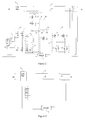
- FIG 1 is a block diagram of a line interactive UPS of the present invention.
- the line interactive UPS of the present invention comprises an AC input 20, an AC output 30, a chargeable and dischargeable device 19, a DC/AC inverter 1, a rectifying circuit 14, a rectifying and buck circuit 15, a boost circuit 16, a capacitor C, a full-bridge inverter 5, a charger 2, a switch S and a switch S1.
- the input of the DC/AC inverter 1 is connected across the chargeable and dischargeable device 19 and is configured to convert a DC of the chargeable and dischargeable device 19 into an AC.
- the output of the DC/AC inverter is connected to the input of the rectifying circuit 14, the output of which is connected to the input of the full-bridge inverter 5.
- the input of the rectifying and buck circuit 15 is connected to the AC input 20.
- the rectifying and buck circuit 15 is configured to rectify the AC of the AC input 20 and decrease the voltage of the AC, and output the resulting AC to the input of the full-bridge inverter 5, or rectify the AC of the AC input 20 and output the resulting AC to the input of the boost circuit 16.
- the output of the boost circuit 16 is connected to the input of the full-bridge inverter 5.
- the switch S is configured to selectively connect the AC input 20 or the output of the full-bridge inverter 5 to the AC output 30.
- the input of the full-bridge inverter 5 is connected across the capacitor C.
- the input of the charger 2 is connected to the AC output 30, and the output of the charger 2 is connected across the chargeable and dischargeable device 19, in order to charge the chargeable and dischargeable device 19 with the AC of the AC output 30.
- the chargeable and dischargeable device 19 can be a chargeable and dischargeable battery or battery pack. It can also be a combination of a chargeable and dischargeable battery or battery pack, a protection switch and a capacitor or capacitor pack, wherein the chargeable and dischargeable battery or battery pack and the protection switch are connected in series, and are then connected in parallel to the capacitor or capacitor pack.
- the paralleled capacitor or capacitor pack can be frequently charged and discharged, thereby reducing the charge and discharge times of the battery or battery pack, and thus protecting the battery or battery pack effectively.
- the charger 2 When the voltage of the AC input 20 is equal to the required voltage of the AC output 30, the AC input 20 is directly connected to the AC output 30. In this case, if the voltage across the chargeable and dischargeable device 19 is less than rated voltage of the chargeable and dischargeable device 19, the charger 2 is controlled to charge the chargeable and dischargeable device 19. When the voltage across the chargeable and dischargeable device 19 becomes equal to the rated voltage, the charger 2 is controlled to stop charging.
- the switch S is controlled such that the output of the full-bridge inverter 5 is connected to the AC output 30
- the DC/AC inverter 1 is controlled such that the chargeable and dischargeable device 19 discharges and outputs an AC
- the full-bridge inverter 5 is controlled to work in pulse width modulation mode so as to provide the required AC to the AC output 30.
- the switch S When the voltage of the AC input 20 is greater than the required voltage of the AC output, the switch S is controlled such that the output of the full-bridge inverter 5 is connected to the AC output 30, the DC/AC inverter 1 stops working, the rectifying and buck circuit 15 is controlled to rectify the AC of the AC input 20 and decrease the voltage of the AC, and output the resulting AC to the input of the full-bridge inverter 5 via the switch S1, and the full-bridge inverter 5 is controlled to work in pulse width modulation mode so as to provide the required AC to the AC output 30.
- the switch S When the voltage of the AC input 20 is less than the required voltage of the AC output 30, the switch S is controlled such that the output of the full-bridge inverter 5 is connected to the AC output 30, the DC/AC inverter 1 stops working, the rectifying and buck circuit 15 is controlled to rectify the AC of the AC input 20 and output it to the input of the boost circuit 16 via the switch S1, and the boost circuit 16 and the full-bridge inverter 5 are controlled to work in pulse width modulation mode so as to provide the required AC to the AC output 30. In this state, the rectifying and buck circuit 15 only provides rectifying effect, without decreasing the voltage.
- the AC output 30 may be connected with a resistive load, capacitive load or no load.
- the switch S is controlled such that the output of the full-bridge inverter 5 is connected to the AC output 30, the full-bridge inverter 5 is controlled to work in pulse width modulation mode, the charger 2 is controlled to charge the chargeable and dischargeable device 19, and the following two steps are performed alternately:
- the switch S is controlled such that the output of the full-bridge inverter 5 is connected to the AC output 30, the full-bridge inverter 5 is controlled to work in pulse width modulation mode, the charger 2 is controlled to charge the chargeable and dischargeable device 19, and the following two steps are performed alternately:
- the DC/AC inverter 1, the charger 2, the rectifying circuit 14, the rectifying and buck circuit 15, the boost circuit 16, the full-bridge inverter 5, the chargeable and dischargeable device 19 illustrated in the figure 1 may take any form of circuit known in the art which can achieve its function, so as to achieve the above operating modes.
- the rectifying and buck circuit 15 can achieve the function of converting an AC to a DC, and is operative to provide a voltage-decreased DC.
- FIG. 2 is a circuit diagram of a line interactive UPS of a preferred embodiment of the present invention.
- the input of the DC/AC inverter 1 is connected across the chargeable and dischargeable device 19, the output of the DC/AC inverter 1 is connected to the input of a full-bridge rectifying circuit 6.
- the full-bridge rectifying circuit 6 comprises diodes D1-D4, wherein the anodes of the diodes D1 and D3 act as an input of the full-bridge rectifying circuit 6, and the cathode of the diode D1 and the anode of the diode D2 act as an output of the full-bridge rectifying circuit 6.
- the cathode of the diode D1 is defined as a positive or positive terminal of the output of the full-bridge rectifying circuit 6, and the anode of the diode D2 is defined as a negative or negative terminal of the output of the full-bridge rectifying circuit 6.
- the boost circuit 4 comprises an inductor L1, a diode D9, a metal-oxide-semiconductor field-effect transistor T3, wherein one terminal of the inductor L1 and the source of the metal-oxide-semiconductor field-effect transistor T3 act as an input of the boost circuit 4, the input of which is connected to the output of the full-bridge rectifying circuit 6.
- the cathode of the diode D9 and the source of the metal-oxide-semiconductor field-effect transistor T3 act as an output of the boost circuit 4.
- the full-bridge inverter 5 comprises metal-oxide-semiconductor field-effect transistors T4-T7, wherein the metal-oxide-semiconductor field-effect transistors T4 and T5 are connected and act as a bridge arm, the metal-oxide-semiconductor field-effect transistors T6 and T7 are connected and act as another bridge arm, the drain of the metal-oxide-semiconductor field-effect transistor T4 and the source of the metal-oxide-semiconductor field-effect transistor T5 act as an input of the full-bridge inverter 5 which connects to the output of the boost circuit 4, the source of the metal-oxide-semiconductor field-effect transistor T4 and the source of the metal-oxide-semiconductor field-effect transistor T6 act as an
- a cable 7 and a cable 8 act as an electrical connection loop between the AC input 20 and the AC output 30, wherein the AC input 20 is connected to the mains supply and the AC output 30 is connected to a load (not shown).
- An electro-magnetic interference (EMI) filter 3 is connected between the AC input 20 and the AC output 30, and is configured to filter harmful high frequency noise in the mains supply.
- a switch S is connected between the EMI filter 3 and the AC output 30, and is controlled to selectively connect the AC input 20 or the output of the full-bridge inverter 5 to the AC output 30.
- a rectifying and buck circuit 21 comprises a bi-directional switch 9, a full-bridge rectifying circuit 11 and an inductor L2.
- the bi-directional switch 9 comprises a metal-oxide-semiconductor field-effect transistor T1 having an anti-parallel diode D7 and a metal-oxide-semiconductor field-effect transistor T2 having an anti-parallel diode D8.
- the source of the metal-oxide-semiconductor field-effect transistor T1 is connected to the source of the metal-oxide-semiconductor field-effect transistor T2, the drain of the metal-oxide-semiconductor field-effect transistor T2 is connected to the anode of the diode D5, the drain of the metal-oxide-semiconductor field-effect transistor T1 is connected to the cable 7 which connects between the EMI filter 3 and the switch S, the anode of a diode D10 is connected to the cable 8 which connects between the EMI filter 3 and the switch S.
- the full-bridge rectifying circuit 11 comprises a diode D5, D6, D10 and D11.
- a terminal with higher voltage of an output of the full-bridge rectifying circuit 11 is defined as its positive terminal or positive.
- the cable 7 and cable 8 are connected to the input of the full-bridge rectifying circuit 11 via the bi-directional switch 9.
- One terminal of the inductor L2 is connected to the
- the input of the charger 2 is connected to the AC output 30, and the output of the charger 2 is connected across the chargeable and dischargeable device 19.
- the charger 2 is configured to charge the chargeable and dischargeable device 19 with electric energy of the AC output 30 when the charger is in operation.
- the bi-directional switch 9 may be replaced with a bi-directional thyristor, and the switch S may be any other switch which can achieve switching, for example, a relay.
- a line interactive UPS may exclude the EMI filter 3.
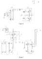
- FIG 3 is an equivalent circuit diagram of the line interactive UPS shown in figure 2 in the bypass mode.
- the switch S is controlled such that the AC input 20 connects to the AC output 30, the bi-directional switch 9 is disconnected, the DC/AC inverter 1, the boost circuit 4 and the full-bridge inverter 5 are controlled to stop working, thus the AC input 20 is directly supplied to the AC output 30.
- the charger 2 is controlled to charge the chargeable and dischargeable device 19.
- the charger 2 stops working.
- FIG 4 is an equivalent circuit diagram of the line interactive UPS shown in figure 2 in the back-up mode.
- the switch S is controlled such that the output of the full-bridge inverter 5 is connected to the AC output 30, the bi-directional switch 9 is disconnected, the metal-oxide-semiconductor field-effect transistor T3 is in the off state such that the boost circuit 4 stops working, the DC/AC inverter 1 is controlled to work in pulse width modulation mode so as to convert DC of the chargeable and dischargeable device 19 into AC, which is then rectified by the full-bridge rectifying circuit 6 to provide a pulsating DC at the input of the full-bridge inverter 5, and the full-bridge inverter 5 is controlled to work in pulse width modulation mode so as to provide the required AC to the AC output 30. Therefore, the AC output 30 can be powered by the chargeable and dischargeable battery B in the backup mode.
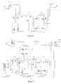
- FIG 5 is an equivalent circuit diagram of the line interactive UPS shown in figure 2 in the line mode to decrease voltage.
- the switch S is controlled such that the output of the full-bridge inverter 5 is connected to the AC output 30.
- the DC/AC inverter 1 stops working
- the metal-oxide-semiconductor field-effect transistor T3 is turned off such that the boost circuit 4 stops working
- the bi-directional 9 is controlled to work in pulse width modulation mode, providing pulse width modulation signals to the metal-oxide-semiconductor field-effect transistors T1 and T2 to make them turn on at the same time or turn off at the same time.
- the full-bridge rectifying circuit 6 and full-bridge rectifying circuit 11 form a continuous current circuit
- the rectifying and buck circuit 15 rectifies the AC of the AC input 20 and decreases the voltage of the AC, thus a pulsating DC is obtained at the input of the full-bridge inverter 5, and the full-bridge inverter 5 is controlled to work in pulse width modulation mode so as to provide the required AC to the AC output 30. As a result, a stable voltage is outputted.
- the controlling method is simple and the power consumption of the bi-directional switch 9 can be reduced.
- the bi-directional switch 9 is controlled to work in pulse width modulation mode, during the positive half cycle of AC of the AC input 20, the metal-oxide-semiconductor field-effect transistor T2 may be turned off and a pulse width modulation signal may be provided to the metal-oxide-semiconductor field-effect transistor T1, and during the negative half cycle of AC of the AC input 20, the metal-oxide-semiconductor field-effect transistor T1 may be turned off and a pulse width modulation signal may be provided to the metal-oxide-semiconductor field-effect transistor T2.
- the charger 2 may be utilized to charge the chargeable and dischargeable device 19. When the voltage across the chargeable and dischargeable device 19 is equal to the rated voltage or a
- FIG 6 is an equivalent circuit diagram of the line interactive UPS shown in figure 2 in the line mode to increase voltage.
- the switch S is controlled such that the output of the full-bridge inverter 5 is connected to the AC output 30, the DC/AC inverter 1 stops working, and the bi-directional switch 9 is always in the conducting state.
- the rectifying and buck circuit 21 only rectifies the AC of the AC input 20, which is converted to DC after being rectified by the full-bridge rectifying circuit 11.
- the boost circuit 4 is controlled to work in pulse width modulation mode so as to obtain a voltage-increased pulsating DC at the output of the boost circuit 4.
- the full-bridge inverter 5 is controlled to work in pulse width modulation mode so as to obtain the required AC at the AC output 30.
- the charger 2 may be utilized to charge the chargeable and dischargeable device 19. When the voltage across the chargeable and dischargeable device 19 is equal to the rated voltage or a percentage of the rated voltage, the charger 2 stops working.
- Figure 7 is a circuit diagram of the line interactive UPS shown in figure 2 connected to a capacitive load, wherein the power required by the capacitive load is less than the power provided by the AC input 20.
- the circuit of figure 7 may further comprise a detecting device for detecting load conditions, for example voltage and power required by the load, and the type of the load, and transmitting a detection signal to a controlling device of the UPS, which controls the operating mode of the circuit according to the detection signal.
- the detecting device may be any form that achieves the above function.
- FIG. 8 is an equivalent circuit diagram of the line interactive UPS shown in figure 7 in the line mode to decrease voltage, wherein the capacitive load is powered by the AC input.
- the switch S is controlled such that the output of the full-bridge inverter 5 is connected to the AC output 30, the metal-oxide-semiconductor field-effect transistor T3 is turned off such that the boost circuit 4 stops working all the time, the charger 2 is controlled to charge the chargeable and dischargeable device 19, the DC/AC inverter 1 stops working, the bi-directional switch 9 is controlled to work in pulse width modulation mode so as to obtain a voltage-decreased pulsating DC at the input of the full-bridge inverter 5, and the full-bridge inverter 5 is controlled to work in pulse width modulation mode so as to obtain the required AC at the AC output 30, wherein the method for controlling the bi-directional switch 9 in figure 8 is the same as that in figure 5 , and thus not discussed here.
- Figure 10 is a timing diagram of a process implemented by the line interactive UPS shown in figure 7 in the line mode to decrease voltage, wherein a high value of the rectifying and buck circuit operating status indicates that the bi-directional switch 9 works in pulse width modulation mode such that the rectifying and buck circuit 21 achieves the functions of rectifying and decreasing voltage at the same time, and a low value of the operating status indicates that the bi-directional switch 9 is in the off state all the time.
- a high value of DC/AC inverter operating status indicates that the DC/AC inverter 1 works in pulse width modulation mode
- a low value of the operating status indicates that the DC/AC inverter 1 stops working.
- the charger 2 is controlled to charge the chargeable and dischargeable device 19 such that the voltage across the chargeable and dischargeable device 19 gradually increases from a first threshold voltage U 1 to a second threshold voltage U 2 .
- the bi-directional switch 9 of the rectifying and buck circuit 21 works in pulse width modulation mode and the DC/AC inverter 1 stops working.
- the bi-directional switch 9 is disconnected, and an equivalent circuit is shown in figure 9 .
- the DC/AC inverter 1 is controlled to work in pulse width modulation mode so as to convert a DC of the chargeable and dischargeable device 19 into an AC and output it.
- a pulsating DC is obtained at the input of the full-bridge inverter 5 after the AC is rectified by the full-bridge rectifying circuit 6.
- the full-bridge inverter 5 is controlled to work in pulse width modulation mode so as to output the required AC to the capacitive load 10. In the process of the chargeable and dischargeable device 19 supplying power to the capacitive load 10, the voltage across the chargeable and dischargeable device 19 gradually decreases from the second threshold voltage U 2 .
- the charger 2 recharges the chargeable and dischargeable device 19 by using a portion of the electrical energy at the AC input 20 when the AC input 20 provides electrical power to the AC output 30.
- the AC input 20 is controlled not to provide electrical power to the AC output 30, and the chargeable and dischargeable device 19 is controlled to provide electrical power to the AC output 30. Therefore, a required sinusoidal voltage across the capacitive load 10 will be obtained, and the impact and influence caused by the inrush current to the full-bridge 5 is reduced.
- FIG 11 is an equivalent circuit diagram of the line interactive UPS shown in figure 7 in the line mode to increase voltage, wherein the capacitive load is powered by the AC output.
- the switch S is controlled such that the output of the full-bridge inverter 5 is connected to the AC output 30, the charger 2 is controlled to charge the chargeable and dischargeable device 19 such that the voltage across the chargeable and dischargeable device 19 gradually increases from the first threshold voltage U 1 to the second threshold voltage U 2 .
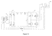
- the bi-directional switch 9 is in the on state (i.e., equivalent to a wire), the boost circuit 4 works in pulse width modulation mode and the DC/AC inverter 1 stops working. An equivalent circuit during this period is shown in figure 11 . After the voltage across the chargeable and dischargeable device 19 increases to the second threshold voltage U 2 , the bi-directional switch 9 is turned off, and the metal-oxide-semiconductor field-effect transistor T3 is turned off such that the boost circuit 4 stops working. An equivalent circuit at this time is shown in figure 12 . The DC/AC inverter 1 is controlled to work in pulse width modulation mode so as to convert DC of the chargeable and dischargeable device 19 into AC.
- a pulsating DC is obtained at the input of the full-bridge inverter 5 after the AC is rectified by the full-bridge rectifying circuit 6.
- the full-bridge inverter 5 is controlled to work in pulse width modulation mode so as to output the required AC to the capacitive load 10.
- the voltage across the chargeable and dischargeable device 19 gradually decreases from the second threshold voltage U 2 .
- the operation mode of the circuit is the same as that of the equivalent circuit shown in figure 11 again.
- the operation mode of the circuit is the same as that of the equivalent circuit shown in figure 12 again. According to the controlling method of the circuit shown in figures 11 and 12 , a required sinusoidal voltage across the capacitive load 10 will be obtained, and the impact and influence caused by the inrush current to the full-bridge 5 is reduced.
- a timing diagram of a controlling method for boosting voltage in line mode based on the equivalent circuits shown in figures 11 and 12 is similar to the timing diagram shown in figure 10 , which is not discussed here.
- the difference is that the operating status of the rectifying and buck circuit in figure 10 is replaced by an operating status of a boost circuit, wherein a high value of the boost circuit operating status indicates that the bi-directional switch 9 is in on state and the boost circuit 4 works in pulse width modulation mode, and a low value of the boost circuit operating status indicates that the bi-directional switch 9 is in off state and the boost circuit 4 stops working.
- the chargeable and dischargeable device 19 provides power to the capacitive load 10 based on the same equivalent circuit diagram (i.e. figure 9 and figure 12 ) when the power provided by the AC input 20 is greater than the required power for the capacitive load 10.
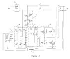
- FIG. 13 is a circuit diagram of a line interactive UPS according to a second embodiment of the present invention, which is similar to that shown in figure 2 .
- the difference is that figure 13 does not have the inductor L2 and the diodes D10 and D11.
- Diodes D3, D4, D5 and D6 constitute a full-bridge rectifying circuit 22.
- the cables 7 and 8 are connected to an input of the full-bridge rectifying circuit 22 via the bi-directional switch 9.
- the controlling method of the UPS shown in figure 13 is the same as that of the UPS shown in figure 2 , which is not discussed here.
- the line interactive UPS of the present embodiment has fewer components, reduced cost and lower energy consumption.
- Figure 14 is a circuit diagram of a line interactive UPS according to a third embodiment of the present invention, which is similar to that shown in figure 13 .
- the difference is that figure 14 does not have the bi-directional switch 9, but comprises a metal-oxide-semiconductor field-effect transistor T8 and a diode D12, and the cable 7 is directly connected to the anode of the diode D5.
- the metal-oxide-semiconductor field-effect transistor T8, diode D12 and inductor L1 constitute a buck circuit 13, wherein the buck circuit 13 and the boost circuit 4 share the inductor L1.
- the full-bridge rectifying circuit 22 and buck circuit 13 constitute a rectifying and buck circuit for rectifying and decreasing the AC of the AC input 20.
- the line interactive UPS of the present embodiment has fewer components and reduced cost.
- the buck circuit 13 and boost circuit 4 may not share the inductor L1.
Landscapes
- Engineering & Computer Science (AREA)
- Power Engineering (AREA)
- Business, Economics & Management (AREA)
- Emergency Management (AREA)
- Inverter Devices (AREA)
- Charge And Discharge Circuits For Batteries Or The Like (AREA)
- Dc-Dc Converters (AREA)
- Rectifiers (AREA)
Abstract
Description
- The present invention relates to an UPS, and particularly, to a line interactive UPS and a controlling method thereof.
- An UPS can continuously provide power supply to electrical equipments, and has been widely researched and utilized. The UPS can be classified into three types according to its operating mode: back-up type, line type and line interactive type.
- The line interactive UPS directly provides mains supply to load when the mains supply is normal, and provides power to the load by a battery during the failure of the mains supply. If the voltage of the mains supply is relatively high or low, after being converted by an inverter, the output voltage of the UPS will be higher or lower than a the required voltage for the load. In order to provide a stable output voltage of the line interactive UPS, an automatic voltage regulator (AVR) is usually connected to the input for the mains supply, in order to regulate the output voltage of the UPS. The automatic voltage regulator has high reliability and wide adjustment range for the input voltage.
- However, the automatic voltage regulator has a large size, a large weight, high cost and energy consumption, which directly lead to reduction of electrical energy utilization efficiency and increased cost. Therefore, it is desirable to provide an UPS which can provide stable AC voltage without the need of an AVR.
- In order to resolve the above-mentioned technical problem, the present invention provides a line interactive UPS, which comprises:
- an AC input and an AC output;
- a chargeable and dischargeable device;
- a DC/AC inverter, an input of which is connected across the chargeable and dischargeable device;
- a rectifying circuit, an input of which is connected to an output of the DC/AC inverter;
- a full-bridge inverter, an input of which is connected to an output of the rectifying circuit;
- a capacitor, the two terminals of which are connected to the input of the full-bridge inverter;
- a switch, which is controlled to connect the AC input or an output of the full-bridge inverter to the AC output;
- a charger, an input of which is connected to the AC output, and an output of which is connected across the chargeable and dischargeable device;
- a boost circuit, an output of which is connected to the input of the full-bridge inverter; and
- a rectifying and buck circuit, which is controlled to provide a rectified output or a rectified and voltage-decreased output, wherein an input of the rectifying and buck circuit is connected to the AC input, and the rectifying and buck circuit is operative to provide a pulsating DC to the boost circuit or the full-bridge inverter.
- Preferably, the rectifying and buck circuit comprises a bi-directional switch, a first full-bridge rectifying circuit and an inductor, wherein the first full-bridge rectifying circuit includes an input and an output, the AC input is connected to the input of the first full-bridge rectifying circuit via the bi-directional switch, a terminal of the inductor is connected to the positive of the output of the first full-bridge rectifying circuit.
- Preferably, the bi-directional switch comprises a first metal-oxide-semiconductor field-effect transistor having an anti-parallel diode and a second metal-oxide-semiconductor field-effect transistor having an anti-parallel diode, the source of the first metal-oxide-semiconductor field-effect transistor is connected to the source of the second metal-oxide-semiconductor field-effect transistor, the drain of the second metal-oxide-semiconductor field-effect transistor is connected to the anode of a third diode, the drain of the first metal-oxide-semiconductor field-effect transistor is connected to a terminal of the AC input.
- Preferably, the inductor constitutes a part of the boost circuit, which increases voltage through the inductor.
- Preferably, the rectifying and buck circuit comprises a first full-bridge rectifying circuit and a buck circuit, the first full-bridge rectifying circuit includes an input and an output, the input of the first full-bridge rectifying circuit is connected to the AC input, the output of the first full-bridge rectifying circuit connecting to an input of the buck circuit, an output of the buck circuit acts as an output of the rectifying and buck circuit.
- Preferably, the rectifying circuit comprises a second full-bridge rectifying circuit, the first full-bridge rectifying circuit and the second full-bridge rectifying circuit share two diodes.
- Preferably, the chargeable and dischargeable device comprises a protection switch, a storage capacitor and a chargeable and dischargeable battery, wherein the protection switch and the chargeable and dischargeable battery are connected in series, and are then connected in parallel to the storage capacitor.
- A embodiment of the present invention provides a controlling method of the line interactive UPS, when the voltage of the AC input is greater than the required voltage for the AC output, the switch is controlled to connect the output of the full-bridge inverter to the AC output, the DC/AC inverter stops working, the rectifying and buck circuit is controlled to rectify an AC of the AC input and decrease the voltage of the AC and provide a pulsating DC to the full-bridge inverter, and the full-bridge inverter is controlled to work in pulse width modulation mode so as to provide the required AC to the AC output.
- Another embodiment of the present invention provides a controlling method of the line interactive UPS, when the voltage of the AC input is less than the required voltage for the AC output, the switch is controlled to connect the output of the full-bridge inverter to the AC output, the DC/AC inverter stops working, the rectifying and buck circuit is controlled to rectify an AC of the AC input and provide a pulsating DC to the boost circuit, and the boost circuit and the full-bridge inverter are controlled to work in pulse width modulation mode so as to provide the required AC to the AC output.
- Another embodiment of the present invention provides a controlling method of the line interactive UPS, when the voltage of the AC input is greater than the required voltage for the AC output and the AC output is connected to a capacitive load requiring a power which is less than the power provided by the AC input, the switch is controlled to connect the output of the full-bridge inverter to the AC output, the full-bridge inverter is controlled to work in pulse width modulation mode, the charger is controlled to charge the chargeable and dischargeable device, and the following two steps are performed alternately:
- controlling the DC/AC inverter to stop working, controlling the rectifying and buck circuit to rectify an AC of the AC input and decrease the voltage of the AC and provide a pulsating DC to the full-bridge inverter, such that the voltage across the chargeable and dischargeable device increases from a first threshold voltage to a second threshold voltage which is greater than the first threshold voltage, and providing the required voltage to the AC output;
- controlling the rectifying and buck circuit to stop working, controlling the DC/AC inverter to work in pulse width modulation mode, such that the voltage across the chargeable and dischargeable device decreases from the second threshold voltage to the first threshold voltage, and providing the required voltage to the AC output.
- Another embodiment of the present invention provides a controlling method of the line interactive UPS, when the voltage of the AC input is less than the required voltage for the AC output and the AC output is connected to a capacitive load requiring a power which is less than the power provided by the AC input, the switch is controlled to connect the output of the full-bridge inverter to the AC output, the full-bridge inverter is controlled to work in pulse width modulation mode, the charger is controlled to charge the chargeable and dischargeable device, and the following two steps are performed alternately:
- controlling the DC/AC inverter to stop working, controlling the rectifying and buck circuit to rectify an AC of the AC input and provide a pulsating DC to the boost circuit, such that the voltage across the chargeable and dischargeable device increases from a first threshold voltage to a second threshold voltage which is greater than the first threshold voltage, controlling the boost circuit to work in pulse width modulation mode and providing the required AC to the AC output;
- controlling the rectifying and buck circuit to stop working, controlling the DC/AC inverter to work in pulse width modulation mode, such that the voltage across the chargeable and dischargeable device decreases from the second threshold voltage to the first threshold voltage, and providing the required AC to the AC output.
- The line interactive UPS of the present invention can provide a stable AC at the output, with simple circuit structure, fewer components and reduced cost, and improve the utilization efficiency of electrical energy. According the controlling method of the line interactive UPS, the UPS of the present invention can be applied to any kind of loads, avoids the distortion of output waveform, and avoids a large inrush current which may damage the inverter of the UPS.
- Below, embodiments of the present invention are described in detail with reference to the drawings, wherein:
-
Figure 1 is a block diagram of a line interactive UPS of the present invention. -
Figure 2 is a circuit diagram of a line interactive UPS of a first embodiment of the present invention. -
Figure 3 is an equivalent circuit diagram of the line interactive UPS shown infigure 2 in the bypass mode. -
Figure 4 is an equivalent circuit diagram of the line interactive UPS shown infigure 2 in the back-up mode. -
Figure 5 is an equivalent circuit diagram of the line interactive UPS shown infigure 2 in the line mode to decrease voltage. -
Figure 6 is an equivalent circuit diagram of the line interactive UPS shown infigure 2 in the line mode to increase voltage. -
Figure 7 is a circuit diagram of the line interactive UPS shown infigure 2 connected to a capacitive load. -
Figure 8 is an equivalent circuit diagram of the line interactive UPS shown infigure 7 in the line mode to decrease voltage, wherein the capacitive load is powered by the AC output. -
Figure 9 is an equivalent circuit diagram of the line interactive UPS shown infigure 7 in the line mode to decrease voltage, wherein the capacitive load is powered by the chargeable and dischargeable device. -
Figure 10 is a timing diagram of a process implemented by the line interactive UPS shown infigure 7 in the line mode to decrease voltage.Figure 11 is an equivalent circuit diagram of the line interactive UPS shown infigure 7 in the line mode to increase voltage, wherein the capacitive load is powered by the AC output. -
Figure 12 is an equivalent circuit diagram of the line interactive UPS shown infigure 7 in the line mode to increase voltage, wherein the capacitive load is powered by the chargeable and dischargeable device. -
Figure 13 is a circuit diagram of a line interactive UPS of a second embodiment of the present invention. -
Figure 14 is a circuit diagram of a line interactive UPS of a third embodiment of the present invention. -
- 1
- DC/AC inverter
- 2
- charger
- 3
- electromagnetic interference (EMI) filter
- 4
- boost circuit
- 5
- full-bridge inverter
- 6
- full-bridge rectifying circuit
- 7,8
- cable
- 9
- bi-directional switch
- 10
- capacitive load
- 11
- full-bridge rectifying circuit
- 13
- buck circuit
- 14
- rectifying circuit
- 15
- rectifying and buck circuit
- 16
- boost circuit
- 19
- chargeable and dischargeable device
- 20
- AC input
- 21
- rectifying and buck circuit
- 22
- full-bridge rectifying circuit
- 30
- AC output
- S, S1
- switch
- C
- capacitor
- T1-T8
- metal-oxide-semiconductor field-effect transistor
- D1-D12
- diode
- L1, L2
- inductor
- In order to make the objects, technical solutions and advantages of the present invention more apparent, the present invention is further described in detail by using the specific embodiments below, with reference to the drawings. It should be understand that the specific embodiments described herein are only used for explaining the present invention, and are not intended to limit the present invention.
-
Figure 1 is a block diagram of a line interactive UPS of the present invention. As shown infigure 1 , the line interactive UPS of the present invention comprises anAC input 20, anAC output 30, a chargeable anddischargeable device 19, a DC/AC inverter 1, a rectifyingcircuit 14, a rectifying andbuck circuit 15, aboost circuit 16, a capacitor C, a full-bridge inverter 5, acharger 2, a switch S and a switch S1. The input of the DC/AC inverter 1 is connected across the chargeable anddischargeable device 19 and is configured to convert a DC of the chargeable anddischargeable device 19 into an AC. The output of the DC/AC inverter is connected to the input of the rectifyingcircuit 14, the output of which is connected to the input of the full-bridge inverter 5. The input of the rectifying andbuck circuit 15 is connected to theAC input 20. The rectifying andbuck circuit 15 is configured to rectify the AC of theAC input 20 and decrease the voltage of the AC, and output the resulting AC to the input of the full-bridge inverter 5, or rectify the AC of theAC input 20 and output the resulting AC to the input of theboost circuit 16. The output of theboost circuit 16 is connected to the input of the full-bridge inverter 5. The switch S is configured to selectively connect theAC input 20 or the output of the full-bridge inverter 5 to theAC output 30. The input of the full-bridge inverter 5 is connected across the capacitor C. The input of thecharger 2 is connected to theAC output 30, and the output of thecharger 2 is connected across the chargeable anddischargeable device 19, in order to charge the chargeable anddischargeable device 19 with the AC of theAC output 30. - The chargeable and
dischargeable device 19 can be a chargeable and dischargeable battery or battery pack. It can also be a combination of a chargeable and dischargeable battery or battery pack, a protection switch and a capacitor or capacitor pack, wherein the chargeable and dischargeable battery or battery pack and the protection switch are connected in series, and are then connected in parallel to the capacitor or capacitor pack. When the charging and discharging process of the chargeable anddischargeable device 19 is frequent, the paralleled capacitor or capacitor pack can be frequently charged and discharged, thereby reducing the charge and discharge times of the battery or battery pack, and thus protecting the battery or battery pack effectively. - When the voltage of the
AC input 20 is equal to the required voltage of theAC output 30, theAC input 20 is directly connected to theAC output 30. In this case, if the voltage across the chargeable anddischargeable device 19 is less than rated voltage of the chargeable anddischargeable device 19, thecharger 2 is controlled to charge the chargeable anddischargeable device 19. When the voltage across the chargeable anddischargeable device 19 becomes equal to the rated voltage, thecharger 2 is controlled to stop charging. - When there does not exist an AC at the
AC input 20, the switch S is controlled such that the output of the full-bridge inverter 5 is connected to theAC output 30, the DC/AC inverter 1 is controlled such that the chargeable anddischargeable device 19 discharges and outputs an AC, and the full-bridge inverter 5 is controlled to work in pulse width modulation mode so as to provide the required AC to theAC output 30. - When the voltage of the
AC input 20 is greater than the required voltage of the AC output, the switch S is controlled such that the output of the full-bridge inverter 5 is connected to theAC output 30, the DC/AC inverter 1 stops working, the rectifying andbuck circuit 15 is controlled to rectify the AC of theAC input 20 and decrease the voltage of the AC, and output the resulting AC to the input of the full-bridge inverter 5 via the switch S1, and the full-bridge inverter 5 is controlled to work in pulse width modulation mode so as to provide the required AC to theAC output 30. - When the voltage of the
AC input 20 is less than the required voltage of theAC output 30, the switch S is controlled such that the output of the full-bridge inverter 5 is connected to theAC output 30, the DC/AC inverter 1 stops working, the rectifying andbuck circuit 15 is controlled to rectify the AC of theAC input 20 and output it to the input of theboost circuit 16 via the switch S1, and theboost circuit 16 and the full-bridge inverter 5 are controlled to work in pulse width modulation mode so as to provide the required AC to theAC output 30. In this state, the rectifying andbuck circuit 15 only provides rectifying effect, without decreasing the voltage. - When the UPS operates in the above two line modes, the
AC output 30 may be connected with a resistive load, capacitive load or no load. - When the voltage of the
AC input 20 is greater than the required voltage for theAC output 30 and theAC output 30 is connected to a capacitive load requiring a power which is less than the power provided by theAC input 20, the switch S is controlled such that the output of the full-bridge inverter 5 is connected to theAC output 30, the full-bridge inverter 5 is controlled to work in pulse width modulation mode, thecharger 2 is controlled to charge the chargeable anddischargeable device 19, and the following two steps are performed alternately: - Controlling the DC/
AC inverter 1 to stop working, controlling the rectifying andbuck circuit 15 to rectify the AC of theAC input 20 and decrease the voltage of the AC, and output the resulting AC to the input of the full-bridge inverter 5, such that the voltage across the chargeable anddischargeable device 19 increases from a first threshold voltage to a second threshold voltage which is greater than the first threshold voltage, and providing the required voltage to theAC output 30; - Controlling the rectifying and
buck circuit 15 to stop working, controlling the DC/AC inverter 1 to work in pulse width modulation mode, such that the voltage across the chargeable anddischargeable device 19 decreases from the second threshold voltage to the first threshold voltage, and providing the required voltage to theAC output 30. - When the voltage of the
AC input 20 is less than the required voltage for theAC output 30 and theAC output 30 is connected to a capacitive load requiring a power which is less than the power provided by theAC input 20, the switch S is controlled such that the output of the full-bridge inverter 5 is connected to theAC output 30, the full-bridge inverter 5 is controlled to work in pulse width modulation mode, thecharger 2 is controlled to charge the chargeable anddischargeable device 19, and the following two steps are performed alternately: - Controlling the DC/
AC inverter 1 to stop working, controlling the rectifying andbuck circuit 15 to rectify the AC of theAC input 20 and output it to the input of theboost circuit 16, such that the voltage across the chargeable anddischargeable device 19 increases from a first threshold voltage to a second threshold voltage which is greater than the first threshold voltage, controlling theboost circuit 16 to work in pulse width modulation mode, and providing the required AC to theAC output 30; - Controlling the rectifying and
buck circuit 15 to stop working, controlling the DC/AC inverter 1 to work in pulse width modulation mode, such that the voltage across the chargeable anddischargeable device 19 decreases from the second threshold voltage to the first threshold voltage, and providing the required AC to theAC output 30. - Those skilled in the art can understand that the DC/
AC inverter 1, thecharger 2, the rectifyingcircuit 14, the rectifying andbuck circuit 15, theboost circuit 16, the full-bridge inverter 5, the chargeable anddischargeable device 19 illustrated in thefigure 1 may take any form of circuit known in the art which can achieve its function, so as to achieve the above operating modes. The rectifying andbuck circuit 15 can achieve the function of converting an AC to a DC, and is operative to provide a voltage-decreased DC. -
Figure 2 is a circuit diagram of a line interactive UPS of a preferred embodiment of the present invention. As shown infigure 2 , the input of the DC/AC inverter 1 is connected across the chargeable anddischargeable device 19, the output of the DC/AC inverter 1 is connected to the input of a full-bridge rectifying circuit 6. The full-bridge rectifying circuit 6 comprises diodes D1-D4, wherein the anodes of the diodes D1 and D3 act as an input of the full-bridge rectifying circuit 6, and the cathode of the diode D1 and the anode of the diode D2 act as an output of the full-bridge rectifying circuit 6. The cathode of the diode D1 is defined as a positive or positive terminal of the output of the full-bridge rectifying circuit 6, and the anode of the diode D2 is defined as a negative or negative terminal of the output of the full-bridge rectifying circuit 6. Theboost circuit 4 comprises an inductor L1, a diode D9, a metal-oxide-semiconductor field-effect transistor T3, wherein one terminal of the inductor L1 and the source of the metal-oxide-semiconductor field-effect transistor T3 act as an input of theboost circuit 4, the input of which is connected to the output of the full-bridge rectifying circuit 6. The cathode of the diode D9 and the source of the metal-oxide-semiconductor field-effect transistor T3 act as an output of theboost circuit 4. The full-bridge inverter 5 comprises metal-oxide-semiconductor field-effect transistors T4-T7, wherein the metal-oxide-semiconductor field-effect transistors T4 and T5 are connected and act as a bridge arm, the metal-oxide-semiconductor field-effect transistors T6 and T7 are connected and act as another bridge arm, the drain of the metal-oxide-semiconductor field-effect transistor T4 and the source of the metal-oxide-semiconductor field-effect transistor T5 act as an input of the full-bridge inverter 5 which connects to the output of theboost circuit 4, the source of the metal-oxide-semiconductor field-effect transistor T4 and the source of the metal-oxide-semiconductor field-effect transistor T6 act as an output of the full-bridge inverter 5. Acable 7 and acable 8 act as an electrical connection loop between theAC input 20 and theAC output 30, wherein theAC input 20 is connected to the mains supply and theAC output 30 is connected to a load (not shown). An electro-magnetic interference (EMI)filter 3 is connected between theAC input 20 and theAC output 30, and is configured to filter harmful high frequency noise in the mains supply. A switch S is connected between theEMI filter 3 and theAC output 30, and is controlled to selectively connect theAC input 20 or the output of the full-bridge inverter 5 to theAC output 30. A rectifying andbuck circuit 21 comprises a bi-directional switch 9, a full-bridge rectifying circuit 11 and an inductor L2. The bi-directional switch 9 comprises a metal-oxide-semiconductor field-effect transistor T1 having an anti-parallel diode D7 and a metal-oxide-semiconductor field-effect transistor T2 having an anti-parallel diode D8. The source of the metal-oxide-semiconductor field-effect transistor T1 is connected to the source of the metal-oxide-semiconductor field-effect transistor T2, the drain of the metal-oxide-semiconductor field-effect transistor T2 is connected to the anode of the diode D5, the drain of the metal-oxide-semiconductor field-effect transistor T1 is connected to thecable 7 which connects between theEMI filter 3 and the switch S, the anode of a diode D10 is connected to thecable 8 which connects between theEMI filter 3 and the switch S. The full-bridge rectifying circuit 11 comprises a diode D5, D6, D10 and D11. A terminal with higher voltage of an output of the full-bridge rectifying circuit 11 is defined as its positive terminal or positive. Thecable 7 andcable 8 are connected to the input of the full-bridge rectifying circuit 11 via the bi-directional switch 9. One terminal of the inductor L2 is connected to the - positive terminal of the full-
bridge rectifying circuit 11, and the other terminal of the inductor L2 and the other terminal of the output of the full-bridge rectifying circuit 11 act as the output of the rectifying andbuck circuit 21. The input of thecharger 2 is connected to theAC output 30, and the output of thecharger 2 is connected across the chargeable anddischargeable device 19. Thecharger 2 is configured to charge the chargeable anddischargeable device 19 with electric energy of theAC output 30 when the charger is in operation. - In other embodiment of the present invention, the bi-directional switch 9 may be replaced with a bi-directional thyristor, and the switch S may be any other switch which can achieve switching, for example, a relay. In a further embodiment, a line interactive UPS may exclude the
EMI filter 3. - The operating principle and controlling method of the line interactive UPS shown in
figure 2 will be described below with reference tofigures 3-8 . -
Figure 3 is an equivalent circuit diagram of the line interactive UPS shown infigure 2 in the bypass mode. When the voltage of theAC input 20 is equal to the required voltage of theAC output 30, which indicates the mains supply is normal, the switch S is controlled such that theAC input 20 connects to theAC output 30, the bi-directional switch 9 is disconnected, the DC/AC inverter 1, theboost circuit 4 and the full-bridge inverter 5 are controlled to stop working, thus theAC input 20 is directly supplied to theAC output 30. If the voltage across the chargeable anddischargeable device 19 is less than its rated voltage or a percentage of the rated voltage, thecharger 2 is controlled to charge the chargeable anddischargeable device 19. When the voltage across the chargeable anddischargeable device 19 is equal to the rated voltage or a percentage of the rated voltage, thecharger 2 stops working. -
Figure 4 is an equivalent circuit diagram of the line interactive UPS shown infigure 2 in the back-up mode. In the back-up mode, the mains supply fails and cannot provide AC. In this case, the switch S is controlled such that the output of the full-bridge inverter 5 is connected to theAC output 30, the bi-directional switch 9 is disconnected, the metal-oxide-semiconductor field-effect transistor T3 is in the off state such that theboost circuit 4 stops working, the DC/AC inverter 1 is controlled to work in pulse width modulation mode so as to convert DC of the chargeable anddischargeable device 19 into AC, which is then rectified by the full-bridge rectifying circuit 6 to provide a pulsating DC at the input of the full-bridge inverter 5, and the full-bridge inverter 5 is controlled to work in pulse width modulation mode so as to provide the required AC to theAC output 30. Therefore, theAC output 30 can be powered by the chargeable and dischargeable battery B in the backup mode. -
Figure 5 is an equivalent circuit diagram of the line interactive UPS shown infigure 2 in the line mode to decrease voltage. When the voltage of theAC input 20 is greater than the required voltage of theAC output 30, the switch S is controlled such that the output of the full-bridge inverter 5 is connected to theAC output 30. In this case, the DC/AC inverter 1 stops working, the metal-oxide-semiconductor field-effect transistor T3 is turned off such that theboost circuit 4 stops working, and the bi-directional 9 is controlled to work in pulse width modulation mode, providing pulse width modulation signals to the metal-oxide-semiconductor field-effect transistors T1 and T2 to make them turn on at the same time or turn off at the same time. When the metal-oxide-semiconductor field-effect transistors T1 and T2 are turned off at the same time, the full-bridge rectifying circuit 6 and full-bridge rectifying circuit 11 form a continuous current circuit, the rectifying andbuck circuit 15 rectifies the AC of theAC input 20 and decreases the voltage of the AC, thus a pulsating DC is obtained at the input of the full-bridge inverter 5, and the full-bridge inverter 5 is controlled to work in pulse width modulation mode so as to provide the required AC to theAC output 30. As a result, a stable voltage is outputted. By making the metal-oxide-semiconductor field-effect transistors T1 and T2 work in pulse width modulation mode and turn on or turn off at the same time, the controlling method is simple and the power consumption of the bi-directional switch 9 can be reduced. When the bi-directional switch 9 is controlled to work in pulse width modulation mode, during the positive half cycle of AC of theAC input 20, the metal-oxide-semiconductor field-effect transistor T2 may be turned off and a pulse width modulation signal may be provided to the metal-oxide-semiconductor field-effect transistor T1, and during the negative half cycle of AC of theAC input 20, the metal-oxide-semiconductor field-effect transistor T1 may be turned off and a pulse width modulation signal may be provided to the metal-oxide-semiconductor field-effect transistor T2. In another embodiment of the present invention, thecharger 2 may be utilized to charge the chargeable anddischargeable device 19. When the voltage across the chargeable anddischargeable device 19 is equal to the rated voltage or a percentage of the rated voltage, thecharger 2 stops working. -
Figure 6 is an equivalent circuit diagram of the line interactive UPS shown infigure 2 in the line mode to increase voltage. When the voltage of theAC input 20 is less than the required voltage for theAC output 30, the switch S is controlled such that the output of the full-bridge inverter 5 is connected to theAC output 30, the DC/AC inverter 1 stops working, and the bi-directional switch 9 is always in the conducting state. The rectifying andbuck circuit 21 only rectifies the AC of theAC input 20, which is converted to DC after being rectified by the full-bridge rectifying circuit 11. Theboost circuit 4 is controlled to work in pulse width modulation mode so as to obtain a voltage-increased pulsating DC at the output of theboost circuit 4. The full-bridge inverter 5 is controlled to work in pulse width modulation mode so as to obtain the required AC at theAC output 30. In another embodiment of the present invention, thecharger 2 may be utilized to charge the chargeable anddischargeable device 19. When the voltage across the chargeable anddischargeable device 19 is equal to the rated voltage or a percentage of the rated voltage, thecharger 2 stops working. -
Figure 7 is a circuit diagram of the line interactive UPS shown infigure 2 connected to a capacitive load, wherein the power required by the capacitive load is less than the power provided by theAC input 20. In another embodiment of the present invention, the circuit offigure 7 may further comprise a detecting device for detecting load conditions, for example voltage and power required by the load, and the type of the load, and transmitting a detection signal to a controlling device of the UPS, which controls the operating mode of the circuit according to the detection signal. Those skilled in the art can understand that the detecting device may be any form that achieves the above function. When the power required by thecapacitive load 10 is less than the power provided by theAC input 20, at the peak point of sine wave of AC of theAC input 20, the stored energy in thecapacitive load 10 will be very large, causing waveform distortion across thecapacitive load 10 and a large amount of inrush current flowing into the full-bridge inverter 5, which are likely to damage the full-bridge inverter 5 and reduce life span of the full-bridge inverter 5. For this case, the present invention also provides an embodiment for solving the above problem. Below, the embodiment is described in detail with reference tofigures 8-12 .Figure 8 is an equivalent circuit diagram of the line interactive UPS shown infigure 7 in the line mode to decrease voltage, wherein the capacitive load is powered by the AC input. When the voltage of theAC input 20 is greater than the required voltage for theAC output 30, since the power provided by theAC input 20 is greater than the power required by the capacitive load, the switch S is controlled such that the output of the full-bridge inverter 5 is connected to theAC output 30, the metal-oxide-semiconductor field-effect transistor T3 is turned off such that theboost circuit 4 stops working all the time, thecharger 2 is controlled to charge the chargeable anddischargeable device 19, the DC/AC inverter 1 stops working, the bi-directional switch 9 is controlled to work in pulse width modulation mode so as to obtain a voltage-decreased pulsating DC at the input of the full-bridge inverter 5, and the full-bridge inverter 5 is controlled to work in pulse width modulation mode so as to obtain the required AC at theAC output 30, wherein the method for controlling the bi-directional switch 9 infigure 8 is the same as that infigure 5 , and thus not discussed here. -
Figure 10 is a timing diagram of a process implemented by the line interactive UPS shown infigure 7 in the line mode to decrease voltage, wherein a high value of the rectifying and buck circuit operating status indicates that the bi-directional switch 9 works in pulse width modulation mode such that the rectifying andbuck circuit 21 achieves the functions of rectifying and decreasing voltage at the same time, and a low value of the operating status indicates that the bi-directional switch 9 is in the off state all the time. In addition, a high value of DC/AC inverter operating status indicates that the DC/AC inverter 1 works in pulse width modulation mode, and a low value of the operating status indicates that the DC/AC inverter 1 stops working. During the operation of the circuit shown infigure 8 , since the power provided by theAC input 20 is greater than the required power for thecapacitive load 10, thecharger 2 is controlled to charge the chargeable anddischargeable device 19 such that the voltage across the chargeable anddischargeable device 19 gradually increases from a first threshold voltage U1 to a second threshold voltage U2. During this period, the bi-directional switch 9 of the rectifying andbuck circuit 21 works in pulse width modulation mode and the DC/AC inverter 1 stops working. When the voltage across the chargeable anddischargeable device 19 increases to the second threshold voltage U2, the bi-directional switch 9 is disconnected, and an equivalent circuit is shown infigure 9 . The DC/AC inverter 1 is controlled to work in pulse width modulation mode so as to convert a DC of the chargeable anddischargeable device 19 into an AC and output it. A pulsating DC is obtained at the input of the full-bridge inverter 5 after the AC is rectified by the full-bridge rectifying circuit 6. The full-bridge inverter 5 is controlled to work in pulse width modulation mode so as to output the required AC to thecapacitive load 10. In the process of the chargeable anddischargeable device 19 supplying power to thecapacitive load 10, the voltage across the chargeable anddischargeable device 19 gradually decreases from the second threshold voltage U2. After the voltage across the chargeable anddischargeable device 19 decreases to the first threshold voltage U1, the operation mode of the circuit is the same as that of the equivalent circuit shown infigure 8 again. After the voltage across the chargeable anddischargeable device 19 increases from the first threshold voltage U1 to the second threshold voltage U2, the operation mode of the circuit is the same as that of the equivalent circuit shown infigure 9 again. According to the controlling method of the circuits shown infigures 8 and 9 , thecharger 2 recharges the chargeable anddischargeable device 19 by using a portion of the electrical energy at theAC input 20 when theAC input 20 provides electrical power to theAC output 30. After the voltage across the chargeable anddischargeable device 19 reaches a predetermined value, theAC input 20 is controlled not to provide electrical power to theAC output 30, and the chargeable anddischargeable device 19 is controlled to provide electrical power to theAC output 30. Therefore, a required sinusoidal voltage across thecapacitive load 10 will be obtained, and the impact and influence caused by the inrush current to the full-bridge 5 is reduced. -
Figure 11 is an equivalent circuit diagram of the line interactive UPS shown infigure 7 in the line mode to increase voltage, wherein the capacitive load is powered by the AC output. When the voltage of theAC input 20 is less than the required voltage for theAC output 30, since the power provided by theAC input 20 is greater than the required power for thecapacitive load 10, the switch S is controlled such that the output of the full-bridge inverter 5 is connected to theAC output 30, thecharger 2 is controlled to charge the chargeable anddischargeable device 19 such that the voltage across the chargeable anddischargeable device 19 gradually increases from the first threshold voltage U1 to the second threshold voltage U2. The bi-directional switch 9 is in the on state (i.e., equivalent to a wire), theboost circuit 4 works in pulse width modulation mode and the DC/AC inverter 1 stops working. An equivalent circuit during this period is shown infigure 11 . After the voltage across the chargeable anddischargeable device 19 increases to the second threshold voltage U2, the bi-directional switch 9 is turned off, and the metal-oxide-semiconductor field-effect transistor T3 is turned off such that theboost circuit 4 stops working. An equivalent circuit at this time is shown infigure 12 . The DC/AC inverter 1 is controlled to work in pulse width modulation mode so as to convert DC of the chargeable anddischargeable device 19 into AC. A pulsating DC is obtained at the input of the full-bridge inverter 5 after the AC is rectified by the full-bridge rectifying circuit 6. The full-bridge inverter 5 is controlled to work in pulse width modulation mode so as to output the required AC to thecapacitive load 10. In the process of the chargeable anddischargeable device 19 supplying power to thecapacitive load 10, the voltage across the chargeable anddischargeable device 19 gradually decreases from the second threshold voltage U2. After the voltage across the chargeable anddischargeable device 19 decreases to the first threshold voltage U1, the operation mode of the circuit is the same as that of the equivalent circuit shown infigure 11 again. After the voltage across the chargeable anddischargeable device 19 increases from the first threshold voltage U1 to the second threshold voltage U2, the operation mode of the circuit is the same as that of the equivalent circuit shown infigure 12 again. According to the controlling method of the circuit shown infigures 11 and12 , a required sinusoidal voltage across thecapacitive load 10 will be obtained, and the impact and influence caused by the inrush current to the full-bridge 5 is reduced. - A timing diagram of a controlling method for boosting voltage in line mode based on the equivalent circuits shown in
figures 11 and12 is similar to the timing diagram shown infigure 10 , which is not discussed here. The difference is that the operating status of the rectifying and buck circuit infigure 10 is replaced by an operating status of a boost circuit, wherein a high value of the boost circuit operating status indicates that the bi-directional switch 9 is in on state and theboost circuit 4 works in pulse width modulation mode, and a low value of the boost circuit operating status indicates that the bi-directional switch 9 is in off state and theboost circuit 4 stops working. - In this embodiment, the chargeable and
dischargeable device 19 provides power to thecapacitive load 10 based on the same equivalent circuit diagram (i.e.figure 9 andfigure 12 ) when the power provided by theAC input 20 is greater than the required power for thecapacitive load 10. - According to the circuit shown in
figure 2 and the above controlling method, since rectifying and decreasing an AC of theAC input 20 and decreasing an AC of theAC input 20 do not happen simultaneously during the operation of the circuit shown infigure 2 , one of the inductors L1 and L2 can be removed. In addition, rectifying the AC outputted by the DC/AC by the full-bridge rectifying circuit 6 and rectifying the AC of theAC input 20 by the full-bridge rectifying circuit 11 do not happen simultaneously. Therefore, the full-bridge rectifying circuit 6 and full-bridge rectifying circuit 11 may share two diodes. -
Figure 13 is a circuit diagram of a line interactive UPS according to a second embodiment of the present invention, which is similar to that shown infigure 2 . The difference is thatfigure 13 does not have the inductor L2 and the diodes D10 and D11. Diodes D3, D4, D5 and D6 constitute a full-bridge rectifying circuit 22. Thecables bridge rectifying circuit 22 via the bi-directional switch 9. The controlling method of the UPS shown infigure 13 is the same as that of the UPS shown infigure 2 , which is not discussed here. By sharing the inductor L1, diode D3 and diode D4, the line interactive UPS of the present embodiment has fewer components, reduced cost and lower energy consumption. -
Figure 14 is a circuit diagram of a line interactive UPS according to a third embodiment of the present invention, which is similar to that shown infigure 13 . The difference is thatfigure 14 does not have the bi-directional switch 9, but comprises a metal-oxide-semiconductor field-effect transistor T8 and a diode D12, and thecable 7 is directly connected to the anode of the diode D5. The metal-oxide-semiconductor field-effect transistor T8, diode D12 and inductor L1 constitute abuck circuit 13, wherein thebuck circuit 13 and theboost circuit 4 share the inductor L1. The full-bridge rectifying circuit 22 andbuck circuit 13 constitute a rectifying and buck circuit for rectifying and decreasing the AC of theAC input 20. By sharing the inductor L1, diode D3 and diode D4, the line interactive UPS of the present embodiment has fewer components and reduced cost. In other embodiments of the present invention, thebuck circuit 13 andboost circuit 4 may not share the inductor L1. - Those skilled in the art will appreciate that the metal-oxide-semiconductor field-effect transistors of the above embodiments can be replaced with IGBT. Although the present invention has been described with reference to preferred embodiments, the present invention is not limited to the embodiments described herein. And the features and operation of the invention as described is susceptible to various modifications and alterations, without departing from the scope of the invention.
Claims (11)
- A line interactive UPS, characterized in that it comprises:an AC input and an AC output;a chargeable and dischargeable device;a DC/AC inverter, an input of which is connected across the chargeable and dischargeable device;a rectifying circuit, an input of which is connected to an output of the DC/AC inverter;a full-bridge inverter, an input of which is connected to an output of the rectifying circuit;a capacitor, the two terminals of which are connected to the input of the full-bridge inverter;a switch, which is controlled to connect the AC input or an output of the full-bridge inverter to the AC output;a charger, an input of which is connected to the AC output, and an output of which is connected across the chargeable and dischargeable device;a boost circuit, an output of which is connected to the input of the full-bridge inverter; anda rectifying and buck circuit, which is controlled to provide a rectified output or a rectified and voltage-decreased output, wherein an input of the rectifying and buck circuit is connected to the AC input, and the rectifying and buck circuit is operative to provide a pulsating DC to the boost circuit or the full-bridge inverter.
- The line interactive UPS according to claim 1, characterized in that the rectifying and buck circuit comprises a bi-directional switch, a first full-bridge rectifying circuit and an inductor, wherein the first full-bridge rectifying circuit includes an input and an output, the AC input is connected to the input of the first full-bridge rectifying circuit via the bi-directional switch, and a terminal of the inductor is connected to the positive of the output of the first full-bridge rectifying circuit.
- The line interactive UPS according to claim 2, characterized in that the bi-directional switch comprises a first metal-oxide-semiconductor field-effect transistor having an anti-parallel diode and a second metal-oxide-semiconductor field-effect transistor having an anti-parallel diode, the source of the first metal-oxide-semiconductor field-effect transistor is connected to the source of the second metal-oxide-semiconductor field-effect transistor, the drain of the second metal-oxide-semiconductor field-effect transistor is connected to the anode of a third diode, and the drain of the first metal-oxide-semiconductor field-effect transistor is connected to a terminal of the AC input.
- The line interactive UPS according to claims 2 or 3, characterized in that the inductor constitutes a part of the boost circuit, which increases voltage through the inductor.
- The line interactive UPS according to claim 1, characterized in that the rectifying and buck circuit comprises a first full-bridge rectifying circuit and a buck circuit, the first full-bridge rectifying circuit includes an input and an output, the input of the first full-bridge rectifying circuit is connected to the AC input, the output of the first full-bridge rectifying circuit is connected to an input of the buck circuit, and an output of the buck circuit acts as an output of the rectifying and buck circuit.
- The line interactive UPS according to claims 2, 3 or 5, characterized in that the rectifying circuit comprises a second full-bridge rectifying circuit, and the first full-bridge rectifying circuit and the second full-bridge rectifying circuit share two diodes.
- The line interactive UPS according to claim 1, characterized in that the chargeable and dischargeable device comprises a protection switch, a storage capacitor and a chargeable and dischargeable battery, wherein the protection switch and the chargeable and dischargeable battery are connected in series, and are then connected in parallel to the storage capacitor.
- A controlling method of the line interactive UPS according to any one of claims 1 to 7, characterized in that when the voltage of the AC input is greater than the required voltage for the AC output, the switch is controlled to connect the output of the full-bridge inverter to the AC output, the DC/AC inverter stops working, the rectifying and buck circuit is controlled to rectify an AC of the AC input and decrease the voltage of the AC, and provide a pulsating DC to the full-bridge inverter, and the full-bridge inverter is controlled to work in pulse width modulation mode so as to provide the required AC to the AC output.
- A controlling method of the line interactive UPS according to any one of claims 1 to 7, characterized in that when the voltage of the AC input is less than the required voltage for the AC output, the switch is controlled to connect the output of the full-bridge inverter to the AC output, the DC/AC inverter stops working, the rectifying and buck circuit is controlled to rectify an AC of the AC input and provide a pulsating DC to the boost circuit, and the boost circuit and the full-bridge inverter are controlled to work in pulse width modulation mode so as to provide the required AC to the AC output.
- A controlling method of the line interactive UPS according to any one of claims 1 to 7, characterized in that when the voltage of the AC input is greater than the required voltage for the AC output and the AC output is connected to a capacitive load requiring a power which is less than the power provided by the AC input, the switch is controlled to connect the output of the full-bridge inverter to the AC output, the full-bridge inverter is controlled to work in pulse width modulation mode, the charger is controlled to charge the chargeable and dischargeable device, and the following two steps are performed alternately:controlling the DC/AC inverter to stop working, controlling the rectifying andbuck circuit to rectify an AC of the AC input and decrease the voltage of the AC and provide a pulsating DC to the full-bridge inverter, such that the voltage across the chargeable and dischargeable device increases from a first threshold voltage to a second threshold voltage which is greater than the first threshold voltage, and providing the required voltage to the AC output;controlling the rectifying and buck circuit to stop working, controlling the DC/AC inverter to work in pulse width modulation mode, such that the voltage across the chargeable and dischargeable device decreases from the second threshold voltage to the first threshold voltage, and providing the required voltage to the AC output.
- A controlling method of the line interactive UPS according to any one of claims 1 to 7, characterized in that when the voltage of the AC input is less than the required voltage for the AC output and the AC output is connected to a capacitive load requiring a power which is less than the power provided by the AC input, the switch is controlled to connect the output of the full-bridge inverter to the AC output, the full-bridge inverter is controlled to work in pulse width modulation mode, the charger is controlled to charge the chargeable and dischargeable device, and the following two steps are performed alternately:controlling the DC/AC inverter to stop working, controlling the rectifying and buck circuit to rectify an AC of the AC input and provide a pulsating DC to the boost circuit, such that the voltage across the chargeable and dischargeable device increases from a first threshold voltage to a second threshold voltage which is greater than the first threshold voltage, controlling the boost circuit to work in pulse width modulation mode, and providing the required AC to the AC output;controlling the rectifying and buck circuit to stop working, controlling the DC/AC inverter to work in pulse width modulation mode, such that the voltage across the chargeable and dischargeable device decreases from the second threshold voltage to the first threshold voltage, and providing the required AC to the AC output.
Applications Claiming Priority (2)
| Application Number | Priority Date | Filing Date | Title |
|---|---|---|---|
| CN201310717600.5A CN104734264B (en) | 2013-12-23 | 2013-12-23 | Line interaction uninterruptible power supply and its control method |
| PCT/CN2014/093295 WO2015096613A1 (en) | 2013-12-23 | 2014-12-08 | Online interactive uninterruptible power supply and control method therefor |
Publications (2)
| Publication Number | Publication Date |
|---|---|
| EP3089316A1 true EP3089316A1 (en) | 2016-11-02 |
| EP3089316A4 EP3089316A4 (en) | 2017-09-06 |
Family
ID=53457857
Family Applications (1)
| Application Number | Title | Priority Date | Filing Date |
|---|---|---|---|
| EP14873436.1A Withdrawn EP3089316A4 (en) | 2013-12-23 | 2014-12-08 | Online interactive uninterruptible power supply and control method therefor |
Country Status (4)
| Country | Link |
|---|---|
| US (1) | US9979227B2 (en) |
| EP (1) | EP3089316A4 (en) |
| CN (1) | CN104734264B (en) |
| WO (1) | WO2015096613A1 (en) |
Cited By (1)
| Publication number | Priority date | Publication date | Assignee | Title |
|---|---|---|---|---|
| EP3206291A1 (en) * | 2016-02-12 | 2017-08-16 | Schneider Electric IT Corporation | Apparatus and method for low frequency power inverter |
Families Citing this family (15)
| Publication number | Priority date | Publication date | Assignee | Title |
|---|---|---|---|---|
| CN106961146B (en) * | 2016-01-08 | 2021-05-14 | 伊顿制造(格拉斯哥)有限合伙莫尔日分支机构 | Uninterruptible power supply and control power supply circuit thereof |
| CN107785987B (en) * | 2016-08-25 | 2023-06-09 | 伊顿制造(格拉斯哥)有限合伙莫尔日分支机构 | Online uninterrupted power supply |
| CN107800185B (en) * | 2016-08-29 | 2023-06-09 | 伊顿制造(格拉斯哥)有限合伙莫尔日分支机构 | Online uninterrupted power supply |
| US10230364B2 (en) | 2017-04-26 | 2019-03-12 | Futurewei Technologies, Inc. | Hybrid power devices |
| CN108092398B (en) * | 2017-12-04 | 2023-12-19 | 西安图为电气技术有限公司 | A controller integrated system |
| CN109888807A (en) * | 2019-03-07 | 2019-06-14 | 深圳供电局有限公司 | Voltage sag compensation devices and systems |
| CN109921500B (en) * | 2019-04-23 | 2025-01-24 | 深圳供电局有限公司 | Output regulation circuit and charger |
| CN110994772A (en) * | 2019-06-11 | 2020-04-10 | 联正电子(深圳)有限公司 | Power distribution system and control method thereof |
| CN111009892A (en) * | 2019-06-11 | 2020-04-14 | 联正电子(深圳)有限公司 | Distribution board |
| CN112751412B (en) * | 2019-10-31 | 2022-08-19 | 华为数字能源技术有限公司 | Communication power supply system |
| CN113098121A (en) * | 2020-01-08 | 2021-07-09 | 伊顿智能动力有限公司 | On-line interactive uninterrupted power supply and control method thereof |
| US12311789B2 (en) * | 2020-12-09 | 2025-05-27 | Lear Corporation | Method and system for controlling on-board battery charger of electric vehicle to accommodate transients in supply voltage |
| JP7672311B2 (en) | 2021-09-01 | 2025-05-07 | 本田技研工業株式会社 | Heating device, method for controlling the heating device, and program |
| CN115498670A (en) * | 2022-09-21 | 2022-12-20 | 珠海瓦特电力设备有限公司 | Implementation method of energy storage control system |
| CN116191901A (en) * | 2023-03-28 | 2023-05-30 | 东莞市灿烨电器有限公司 | Power converter and AC (alternating current) transformation circuit applied by same |
Family Cites Families (11)
| Publication number | Priority date | Publication date | Assignee | Title |
|---|---|---|---|---|
| US5612580A (en) * | 1995-10-10 | 1997-03-18 | Northrop Grumman Corporation | Uninterruptible power system |
| US6774602B2 (en) * | 2002-06-14 | 2004-08-10 | Delphi Technologies, Inc. | Apparatus and method for providing temporary power |
| CN100394667C (en) * | 2003-07-30 | 2008-06-11 | 飞瑞股份有限公司 | Uninterrupted power supply module parallel control method and system thereof |
| CN101123367B (en) * | 2006-08-09 | 2010-09-29 | 台达电子工业股份有限公司 | control method of uninterruptible power supply |
| CN101295934B (en) * | 2007-04-28 | 2012-04-25 | 力博特公司 | Uninterrupted power supply with wide range of input voltage |
| CN101789690B (en) * | 2010-01-26 | 2011-12-14 | 山特电子(深圳)有限公司 | UPS preceding stage electric volt increase station |
| CN102651559A (en) * | 2011-02-23 | 2012-08-29 | 硕天科技股份有限公司 | Uninterruptible power system control method capable of prolonging no-load discharge time |
| WO2012176403A1 (en) | 2011-06-21 | 2012-12-27 | パナソニック株式会社 | Boost-type ac/dc converter |
| US9106103B2 (en) * | 2011-09-23 | 2015-08-11 | Eaton Corporation | Unintteruptible power supply systems and methods employing on-demand energy storage |
| CN103187746B (en) * | 2011-12-31 | 2015-04-29 | 伊顿制造(格拉斯哥)有限合伙莫尔日分支机构 | Uninterruptible power supply topology |
| CN202772647U (en) * | 2012-08-14 | 2013-03-06 | 大连中山海洋消防设备厂 | Special emergency power supply for miniature fire-fighting emergency light fixture |
-
2013
- 2013-12-23 CN CN201310717600.5A patent/CN104734264B/en not_active Expired - Fee Related
-
2014
- 2014-12-08 US US15/107,332 patent/US9979227B2/en active Active
- 2014-12-08 EP EP14873436.1A patent/EP3089316A4/en not_active Withdrawn
- 2014-12-08 WO PCT/CN2014/093295 patent/WO2015096613A1/en not_active Ceased
Cited By (2)
| Publication number | Priority date | Publication date | Assignee | Title |
|---|---|---|---|---|
| EP3206291A1 (en) * | 2016-02-12 | 2017-08-16 | Schneider Electric IT Corporation | Apparatus and method for low frequency power inverter |
| US10211750B2 (en) | 2016-02-12 | 2019-02-19 | Schneider Electric It Corporation | Apparatus and method for low frequency power inverter |
Also Published As
| Publication number | Publication date |
|---|---|
| CN104734264B (en) | 2018-09-28 |
| WO2015096613A1 (en) | 2015-07-02 |
| US20170005511A1 (en) | 2017-01-05 |
| US9979227B2 (en) | 2018-05-22 |
| CN104734264A (en) | 2015-06-24 |
| EP3089316A4 (en) | 2017-09-06 |
Similar Documents
| Publication | Publication Date | Title |
|---|---|---|
| EP3089316A1 (en) | Online interactive uninterruptible power supply and control method therefor | |
| CN104272571B (en) | Power conversion device | |
| RU2501152C2 (en) | Uninsulated charger with bipolar inputs | |
| US12255529B2 (en) | Power factor correction and DC-DC multiplexing converter and uninterruptible power supply including the same | |
| CN103219878A (en) | Capacitor discharging circuit and power converter | |
| EP2873146A1 (en) | Circuit and method for providing hold-up time in a dc-dc converter | |
| CN107800185B (en) | Online uninterrupted power supply | |
| EP2904678B1 (en) | High-efficiency electric conversion and continuity management system for uninterruptible power supplies (ups) and derived apparatuses | |
| RU2012139826A (en) | POWER SUPPLY SYSTEM WITH REDUCED POWER LOSSES, ELECTRONIC DEVICE AND CONTROLLER | |
| US12500424B2 (en) | Power supply system and solar photovoltaic inverter | |
| US20170012465A1 (en) | Ups circuit | |
| US20220399751A1 (en) | Ac switch pfc with integrated charger and dc-dc for online ups systems | |
| US10873219B2 (en) | Contactless power supply device | |
| CN105634108B (en) | Off-line uninterrupted power supply | |
| RU103427U1 (en) | BATTERY-DISCHARGE DEVICE FOR BATTERIES | |
| CA3019619C (en) | Power supply connection device, and charging-discharging control method for same | |
| CN118074305A (en) | An uninterruptible power supply system | |
| CN213782946U (en) | Charging circuit and uninterruptible power supply comprising same | |
| US20260045822A1 (en) | Power Conversion Device And Uninterruptible Power System | |
| US12476481B2 (en) | Uninterruptible power supply | |
| US20230253879A1 (en) | Charger, a multiplexing current conversion circuit and an uninterruptible power supply including the same | |
| US12592628B2 (en) | Solid-state transformer and bus voltage equalization method for solid-state transformer | |
| EP4472022A1 (en) | Uninterruptible power supply, control method and power supply system | |
| US20250119055A1 (en) | Power factor correction and direct current (dc)-dc multiplexing converters | |
| KR200300983Y1 (en) | High Efficient Direct Current Uninterruptible Power Supply Apparatus |
Legal Events
| Date | Code | Title | Description |
|---|---|---|---|
| PUAI | Public reference made under article 153(3) epc to a published international application that has entered the european phase |
Free format text: ORIGINAL CODE: 0009012 |
|
| 17P | Request for examination filed |
Effective date: 20160623 |
|
| AK | Designated contracting states |
Kind code of ref document: A1 Designated state(s): AL AT BE BG CH CY CZ DE DK EE ES FI FR GB GR HR HU IE IS IT LI LT LU LV MC MK MT NL NO PL PT RO RS SE SI SK SM TR |
|
| AX | Request for extension of the european patent |
Extension state: BA ME |
|
| DAX | Request for extension of the european patent (deleted) | ||
| RAP1 | Party data changed (applicant data changed or rights of an application transferred) |
Owner name: EATON MANUFACTURING LP GLASGOW, SUCCURSALE DE MORG |
|
| A4 | Supplementary search report drawn up and despatched |
Effective date: 20170808 |
|
| RIC1 | Information provided on ipc code assigned before grant |
Ipc: H02J 9/06 20060101ALI20170802BHEP Ipc: H02M 7/5387 20070101ALI20170802BHEP Ipc: H02J 9/00 20060101AFI20170802BHEP |
|
| STAA | Information on the status of an ep patent application or granted ep patent |
Free format text: STATUS: THE APPLICATION IS DEEMED TO BE WITHDRAWN |
|
| 18D | Application deemed to be withdrawn |
Effective date: 20190702 |