EP3089004B1 - Vektorfüllsegmentverfahren und -vorrichtung zur reduzierung der anzeigelatenz von berührungsereignissen - Google Patents
Vektorfüllsegmentverfahren und -vorrichtung zur reduzierung der anzeigelatenz von berührungsereignissen Download PDFInfo
- Publication number
- EP3089004B1 EP3089004B1 EP16167584.8A EP16167584A EP3089004B1 EP 3089004 B1 EP3089004 B1 EP 3089004B1 EP 16167584 A EP16167584 A EP 16167584A EP 3089004 B1 EP3089004 B1 EP 3089004B1
- Authority
- EP
- European Patent Office
- Prior art keywords
- touch
- bin
- pixels
- vertex
- values
- Prior art date
- Legal status (The legal status is an assumption and is not a legal conclusion. Google has not performed a legal analysis and makes no representation as to the accuracy of the status listed.)
- Active
Links
Images



Classifications
-
- G—PHYSICS
- G06—COMPUTING OR CALCULATING; COUNTING
- G06F—ELECTRIC DIGITAL DATA PROCESSING
- G06F3/00—Input arrangements for transferring data to be processed into a form capable of being handled by the computer; Output arrangements for transferring data from processing unit to output unit, e.g. interface arrangements
- G06F3/01—Input arrangements or combined input and output arrangements for interaction between user and computer
- G06F3/03—Arrangements for converting the position or the displacement of a member into a coded form
- G06F3/041—Digitisers, e.g. for touch screens or touch pads, characterised by the transducing means
-
- G—PHYSICS
- G06—COMPUTING OR CALCULATING; COUNTING
- G06F—ELECTRIC DIGITAL DATA PROCESSING
- G06F3/00—Input arrangements for transferring data to be processed into a form capable of being handled by the computer; Output arrangements for transferring data from processing unit to output unit, e.g. interface arrangements
- G06F3/01—Input arrangements or combined input and output arrangements for interaction between user and computer
- G06F3/03—Arrangements for converting the position or the displacement of a member into a coded form
- G06F3/041—Digitisers, e.g. for touch screens or touch pads, characterised by the transducing means
- G06F3/0414—Digitisers, e.g. for touch screens or touch pads, characterised by the transducing means using force sensing means to determine a position
- G06F3/04144—Digitisers, e.g. for touch screens or touch pads, characterised by the transducing means using force sensing means to determine a position using an array of force sensing means
-
- G—PHYSICS
- G06—COMPUTING OR CALCULATING; COUNTING
- G06F—ELECTRIC DIGITAL DATA PROCESSING
- G06F3/00—Input arrangements for transferring data to be processed into a form capable of being handled by the computer; Output arrangements for transferring data from processing unit to output unit, e.g. interface arrangements
- G06F3/01—Input arrangements or combined input and output arrangements for interaction between user and computer
- G06F3/03—Arrangements for converting the position or the displacement of a member into a coded form
- G06F3/041—Digitisers, e.g. for touch screens or touch pads, characterised by the transducing means
- G06F3/0416—Control or interface arrangements specially adapted for digitisers
-
- G—PHYSICS
- G06—COMPUTING OR CALCULATING; COUNTING
- G06F—ELECTRIC DIGITAL DATA PROCESSING
- G06F3/00—Input arrangements for transferring data to be processed into a form capable of being handled by the computer; Output arrangements for transferring data from processing unit to output unit, e.g. interface arrangements
- G06F3/01—Input arrangements or combined input and output arrangements for interaction between user and computer
- G06F3/03—Arrangements for converting the position or the displacement of a member into a coded form
- G06F3/041—Digitisers, e.g. for touch screens or touch pads, characterised by the transducing means
- G06F3/0412—Digitisers structurally integrated in a display
-
- G—PHYSICS
- G06—COMPUTING OR CALCULATING; COUNTING
- G06F—ELECTRIC DIGITAL DATA PROCESSING
- G06F3/00—Input arrangements for transferring data to be processed into a form capable of being handled by the computer; Output arrangements for transferring data from processing unit to output unit, e.g. interface arrangements
- G06F3/01—Input arrangements or combined input and output arrangements for interaction between user and computer
- G06F3/03—Arrangements for converting the position or the displacement of a member into a coded form
- G06F3/041—Digitisers, e.g. for touch screens or touch pads, characterised by the transducing means
- G06F3/0416—Control or interface arrangements specially adapted for digitisers
- G06F3/04164—Connections between sensors and controllers, e.g. routing lines between electrodes and connection pads
-
- G—PHYSICS
- G06—COMPUTING OR CALCULATING; COUNTING
- G06F—ELECTRIC DIGITAL DATA PROCESSING
- G06F3/00—Input arrangements for transferring data to be processed into a form capable of being handled by the computer; Output arrangements for transferring data from processing unit to output unit, e.g. interface arrangements
- G06F3/01—Input arrangements or combined input and output arrangements for interaction between user and computer
- G06F3/03—Arrangements for converting the position or the displacement of a member into a coded form
- G06F3/041—Digitisers, e.g. for touch screens or touch pads, characterised by the transducing means
- G06F3/0416—Control or interface arrangements specially adapted for digitisers
- G06F3/0418—Control or interface arrangements specially adapted for digitisers for error correction or compensation, e.g. based on parallax, calibration or alignment
-
- G—PHYSICS
- G06—COMPUTING OR CALCULATING; COUNTING
- G06F—ELECTRIC DIGITAL DATA PROCESSING
- G06F3/00—Input arrangements for transferring data to be processed into a form capable of being handled by the computer; Output arrangements for transferring data from processing unit to output unit, e.g. interface arrangements
- G06F3/01—Input arrangements or combined input and output arrangements for interaction between user and computer
- G06F3/048—Interaction techniques based on graphical user interfaces [GUI]
- G06F3/0487—Interaction techniques based on graphical user interfaces [GUI] using specific features provided by the input device, e.g. functions controlled by the rotation of a mouse with dual sensing arrangements, or of the nature of the input device, e.g. tap gestures based on pressure sensed by a digitiser
- G06F3/0488—Interaction techniques based on graphical user interfaces [GUI] using specific features provided by the input device, e.g. functions controlled by the rotation of a mouse with dual sensing arrangements, or of the nature of the input device, e.g. tap gestures based on pressure sensed by a digitiser using a touch-screen or digitiser, e.g. input of commands through traced gestures
-
- G—PHYSICS
- G06—COMPUTING OR CALCULATING; COUNTING
- G06F—ELECTRIC DIGITAL DATA PROCESSING
- G06F3/00—Input arrangements for transferring data to be processed into a form capable of being handled by the computer; Output arrangements for transferring data from processing unit to output unit, e.g. interface arrangements
- G06F3/01—Input arrangements or combined input and output arrangements for interaction between user and computer
- G06F3/048—Interaction techniques based on graphical user interfaces [GUI]
- G06F3/0487—Interaction techniques based on graphical user interfaces [GUI] using specific features provided by the input device, e.g. functions controlled by the rotation of a mouse with dual sensing arrangements, or of the nature of the input device, e.g. tap gestures based on pressure sensed by a digitiser
- G06F3/0488—Interaction techniques based on graphical user interfaces [GUI] using specific features provided by the input device, e.g. functions controlled by the rotation of a mouse with dual sensing arrangements, or of the nature of the input device, e.g. tap gestures based on pressure sensed by a digitiser using a touch-screen or digitiser, e.g. input of commands through traced gestures
- G06F3/04883—Interaction techniques based on graphical user interfaces [GUI] using specific features provided by the input device, e.g. functions controlled by the rotation of a mouse with dual sensing arrangements, or of the nature of the input device, e.g. tap gestures based on pressure sensed by a digitiser using a touch-screen or digitiser, e.g. input of commands through traced gestures for inputting data by handwriting, e.g. gesture or text
-
- G—PHYSICS
- G06—COMPUTING OR CALCULATING; COUNTING
- G06F—ELECTRIC DIGITAL DATA PROCESSING
- G06F3/00—Input arrangements for transferring data to be processed into a form capable of being handled by the computer; Output arrangements for transferring data from processing unit to output unit, e.g. interface arrangements
- G06F3/14—Digital output to display device ; Cooperation and interconnection of the display device with other functional units
-
- G—PHYSICS
- G06—COMPUTING OR CALCULATING; COUNTING
- G06T—IMAGE DATA PROCESSING OR GENERATION, IN GENERAL
- G06T11/00—Two-dimensional [2D] image generation
- G06T11/20—Drawing from basic elements
- G06T11/23—Drawing from basic elements using straight lines or curves
-
- G—PHYSICS
- G06—COMPUTING OR CALCULATING; COUNTING
- G06T—IMAGE DATA PROCESSING OR GENERATION, IN GENERAL
- G06T11/00—Two-dimensional [2D] image generation
- G06T11/40—Filling planar surfaces by adding surface attributes, e.g. adding colours or textures
Definitions
- Embodiments of the present invention relate to display devices with touch input devices and, more specifically, systems and methods for reducing display lag between a touch input device and a display device.
- a display panel that incorporates an overlaid touch sensor panel may be referred to as a touchscreen display, and may provide an interaction system for touch-enabled computing devices (such as mobile phones, tablet computers, laptop computers, or desktop computers).
- touch-enabled computing devices such as mobile phones, tablet computers, laptop computers, or desktop computers.
- graphics are displayed on the display panel, and a user may interact with these devices by touching the screen (e.g., by using an active stylus, a passive stylus, or a body part such as a finger), thereby providing an intuitive user interface.
- the touch system and display system typically operate independently. Touch events detected by the touch sensor panels are typically processed by high level application software running on an application processor (AP) of the device. That is, the touch system includes a touch controller that processes the signals generated by touch sensors, and that outputs data corresponding to the touch events, such as coordinates, to the AP.
- the AP is generally located externally from the display. The AP processes the touch events, and updates a display composition accordingly to the display driver interface controller (DDIC).
- the DDIC processes video images from AP, and outputs pixel driving signals to the display panel.
- contemporary smart phone devices may exhibit delays of about 100 milliseconds (i.e., about 6 frames at 60 frames per second) when writing on the screen with either a finger or stylus.
- background art includes: EP2799961 , relating to a method and apparatus to reduce display lag using image overlay, and describing a system including a touch path logic configured to receive a plurality of touch events and to generate an output based on the touch events, and a rendering logic configured to receive a video image, receive the output of the touch path logic, combine the video image with overlay data in accordance with the output of the touch path logic to generate a combined display image, and output the combined display image; US2011/0304643 , relating to ink rendering techniques, and describing an input recognized by one or more modules that are executable on one or more processors of a computing device as an ink stroke to be rendered by a display device of the computing device, where an ink stroke is built by the one or more modules using a strip of triangles and the strip of triangles is sent to
- Embodiments of the present invention are directed to reducing the latency between a touch event and a display response to this touch event.
- a method for generating a mask overlay for a display panel corresponding to a touch path on a touch panel, the method including receiving touch path data including touch points corresponding to the touch path, generating vertex points of a vertex array corresponding to the touch points, generating a polygon for a respective set of the vertex points to define edges of the touch path, determining start edges and stop edges of the polygon for a row of pixels, generating a list of bin offset values corresponding to the row of pixels and including bin offsets for indicating the start edges and the stop edges by incrementing a corresponding bin offset by one for each of the start edges, and by decrementing a corresponding subsequent bin offset by one for each of the stop edges, generating an accumulator value corresponding to each of the pixels of each row, determining whether each of the accumulator values is greater than zero or equal to zero, and generating the mask overlay including bits having values determined by
- the method may further include receiving a line width setting, and the vertex points may further correspond to the line width setting.
- the touch path data may further include pressure data corresponding to the touch path, and the vertex points may further correspond to the pressure data.
- the method may further include generating a touch path vector corresponding to a path between adjacent ones of the touch points, and the vertex points may further correspond to the touch path vector.
- Generating the accumulator value may include initializing a count, iterating each bin offset in order, adding to or subtracting from the count based on the bin offsets, and entering the count as the accumulator value corresponding to the iterated bin offset.
- the generating the mask overlay may include generating a "1" of a one bit enable signal in the mask overlay for each of the accumulator values that is greater than zero to indicate that the corresponding ones of the pixels correspond to an edge or an interior of the polygon, and generating a "0" of the one bit enable signal in the mask overlay for each of the accumulator values that is equal to zero.
- the method may further include displaying on a display panel a displayed touch path corresponding to the generated mask overlay.
- a number of the pixels in the row of pixels, a number of the bin offsets in the list of bin offset values, and a number of the bits in the mask overlay, are equal.
- a system for generating a mask overlay for a display panel corresponding to a touch path on a touch panel including, a control logic module configured to receive a vertex array including vertex points, and configured to generate a mask overlay based on the vertex array, wherein the control logic module includes an interpolation calculator configured to determine one or more polygons defining edges of the touch path based on the vertex points, and configured to generate start column offsets and stop column offsets respectively corresponding to start edges and stop edges of the one or more polygons at a row of pixels, a histogram module configured to receive the start and stop column offsets, and configured to generate a list of bin offset values based on the start and stop column offsets, and an accumulator and pixel-fill module configured to receive the list of bin offset values, configured to generate an accumulator value for each pixel of the row of the pixels based on the list of bin offset
- the system may further include a lookup table (LUT) generator configured to receive interpolated touch points corresponding to the touch path, and configured to generate the vertex array based on the interpolated touch points.
- LUT lookup table
- the system may further include a LUT storage module configured to receive and store the vertex array from the LUT generator, and configured to output the vertex array to the control logic module.
- a LUT storage module configured to receive and store the vertex array from the LUT generator, and configured to output the vertex array to the control logic module.
- the LUT generator may include a line width module.
- the LUT generator may be further configured to receive a line width setting, and to generate the vertex array based on the line width setting.
- the LUT generator may be further configured to determine one or more vectors corresponding to the touch path, and to generate the vertex array based on the one or more vectors and based on the line width setting.
- the list of bin offset values may include a plurality of bin offsets, each of which including a value that corresponds to a respective column offset.
- the list of bin offset values may include a same number of bins as a number of the pixels in the row.
- Each of the bins may include an n-bit memory to store a value corresponding to one of the pixels at an edge intersection.
- a method of generating a mask overlay for a display panel corresponding to a touch path on a touch panel including generating polygons corresponding to a vertex array defining edges of the touch path, determining start edges and stop edges of the polygons for a row of pixels, generating bin offsets including values corresponding to the start edges and the stop edges, generating an accumulator value corresponding to each of the pixels based on the bin offsets, and generating the mask overlay including bits having values determined by whether a respective one of the accumulator values is greater than zero.
- the vertex array may include vertex points corresponding to touch points of the touch path.
- the vertex points may further correspond to a pressure on the touch panel.
- spatially relative terms such as “beneath,” “below,” “lower,” “under,” “above,” “upper,” and the like, may be used herein for ease of explanation to describe one element or feature's relationship to another element(s) or feature(s) as illustrated in the figures. It will be understood that the spatially relative terms are intended to encompass different orientations of the device in use or in operation, in addition to the orientation depicted in the figures. For example, if the device in the figures is turned over, elements described as “below” or “beneath” or “under” other elements or features would then be oriented “above” the other elements or features. Thus, the example terms “below” and “under” may encompass both an orientation of above and below. The device may be otherwise oriented (e.g., rotated 90 degrees or at other orientations) and the spatially relative descriptors used herein should be interpreted accordingly.
- the term “substantially,” “about,” and similar terms are used as terms of approximation and not as terms of degree, and are intended to account for the inherent deviations in measured or calculated values that would be recognized by those of ordinary skill in the art. Further, the use of “may” when describing embodiments of the present invention refers to “one or more embodiments of the present invention.” As used herein, the terms “use,” “using,” and “used” may be considered synonymous with the terms “utilize,” “utilizing,” and “utilized,” respectively. Also, the term “exemplary” is intended to refer to an example or illustration.
- the electronic devices or any other relevant devices or components according to embodiments of the present invention described herein may be implemented utilizing any suitable hardware, firmware (e.g. an application-specific integrated circuit), software, or a combination of software, firmware, and hardware.
- the various components of these devices may be formed on one integrated circuit (IC) chip or on separate IC chips.
- the various components of these devices may be implemented on a flexible printed circuit film, a tape carrier package (TCP), a printed circuit board (PCB), or formed on one substrate.
- the various components of these devices may be a process or thread, running on one or more processors, in one or more computing devices, executing computer program instructions and interacting with other system components for performing the various functionalities described herein.
- the computer program instructions are stored in a memory which may be implemented in a computing device using a standard memory device, such as, for example, a random access memory (RAM).
- the computer program instructions may also be stored in other non-transitory computer readable media such as, for example, a CD-ROM, flash drive, or the like.
- a person of skill in the art should recognize that the functionality of various computing devices may be combined or integrated into a single computing device, or the functionality of a particular computing device may be distributed across one or more other computing devices without departing from the scope of the exemplary embodiments of the present invention.
- An algorithm is a self-consistent sequence for achieving a desired result and requiring physical manipulations of physical quantities, which may take the form of electro-magnetic signals capable of being stored, transferred, combined, compared, replicated, reproduced, and otherwise manipulated. Such signals may be referred to as bits, values, elements, symbols, characters, terms, numbers, or the like. These and similar terms are associated with appropriate physical quantities, and are used as representative labels for these quantities.
- processing refers to the action and processes of a computing device or system that manipulates data represented as physical quantities within registers/memories into other data that is also represented by stored/transmitted/displayed physical quantities.
- Embodiments of the present invention provide a new method to fill line segments corresponding to a touch event on a touchscreen display.
- a method of embodiments of the present invention is configured to allow for operation even when touch events are complicated and produce a line that overlaps a previous drawn line.
- the method allows for a lookup table (LUT) to store a set of vertex data, which does not require sorting or classification of a left/right edge of the line segments, and which minimizes the complexity and memory required for the control logic to generate mask data from the LUT.
- embodiments of the present invention allow a user to perceive a faster touch response by displaying an image based on the touch locations in advance of the application processor (AP) rendered image.
- AP application processor
- Software designed for touch interfaces often use direct physical manipulation ofpseudo "real-world” objects and/or the drawing of paths on the screen to provide visual feedback (e.g., for the trace of a finger on a swiping or gesture-based on-screen keyboard, for the trace of a path in a drawing or sketchbook application, and/or for a path drawn in a game).
- a common issue of mobile phones is lag (i.e., lag time, or latency) of the user interface.
- Current mobile phones take up to 200 milliseconds to update the display in response to a touch action.
- the typical display response time to a touch event as measured on a related art smart phone may be about 100 milliseconds, or about 6 frames of video images, based on a refresh rate of 60 frames per second (FPS). This display lag is noticeable by a large portion of users.
- FIG. 1A illustrates the response of a device including a related art touch input processing device
- FIG. 1B illustrates the response of a device including a touch input processing device according to embodiments of the present invention.
- a displayed line (e.g., a generated touch path) 100 has a gap 102 between the position of a finger and a last drawn portion of the displayed line 100.
- the gap 102 corresponds to a noticeable display lag between a time a touch is applied to a touchscreen display, and a time that the displayed line 100 appears on the display. Similar display lag is also typically encountered when using a stylus, whether active or passive.
- the displayed line 100 includes an additional computed portion 104 that is generated by a low latency overlay system of embodiments of the present invention, thereby reducing the display lag/gap 102 perceived by the user, and allowing the user to perceive a faster touch response by overlaying an image (e.g., the computed portion 104) in the touch path in advance of the AP rendered image.
- an image e.g., the computed portion 104
- the perceived display lag may be decreased.
- overlay when used as a verb, refers to combining video images with additional image data, such that the additional image data (e.g., data corresponding to the computed portion 104) replaces, or overlays, some portion of the original video images.
- additional image data e.g., data corresponding to the computed portion 104
- overlay when used as a noun, (e.g., a "mask overlay”) may also refer to the appearance of the computed portion 104 as a result of the additional image data in the combined display image.
- application software may also control a region (e.g., location on the display), color, and rendering operation of the displayed line 100 in response to a touch event.
- FIG. 2 is a schematic illustration of both a related art feedback path, and a low latency feedback path according to an embodiment of the present invention.
- a computing device 250 of the present embodiment is directed to a low latency overlay system that, when compared to related art systems, provides visual feedback more quickly over a low latency path 212 through a touch controller 200 and a display driver interface controller (DDIC) 204, followed by visual images at longer levels of latency over a longer latency path 210 through an application processor 202.
- DDIC display driver interface controller
- a general touch screen system typically operates independently of a corresponding display system.
- a touch sensor panel is configured to detect touch events (e.g., touch inputs, or a user's touches on the touch sensor panel).
- the touch sensor panel is configured to generate touch signals that are supplied to a touch controller 200 (e.g., over a data bus).
- the touch signals output by the touch sensor panel may correspond to signals, or raw data (e.g., measurements of capacitance, voltage, or current corresponding to detected touch locations of the touch sensor panel), or may correspond to computed touch locations based on processed raw data.
- the touch sensor panel of the present embodiment may detect touch events using any object that may be detected by the touch sensor panel, including devices (such as an active stylus or a passive stylus) and body parts (such as a finger or a hand), and may be any type of touch input panel (e.g., resistive touch panels, surface acoustic wave touch panels, capacitive touch panels, infrared touch panels, optical touch panels etc.).
- devices such as an active stylus or a passive stylus
- body parts such as a finger or a hand
- touch input panel e.g., resistive touch panels, surface acoustic wave touch panels, capacitive touch panels, infrared touch panels, optical touch panels etc.
- the touch controller 200 of the present embodiment may process the touch signals from the touch sensor panel, and may output touch points (e.g., coordinates of touch points) to an application processor (AP) 202 via a data bus that is connected to both the AP 202 and a low-latency overlay system (e.g., the low-latency overlay system 310 of FIG. 3 ).
- the touch points may be a stream of data values corresponding to the computed touch locations, and may optionally include pressure data indicating an amount of pressure applied to the touch sensor panel during the touch event.
- the AP 202 is connected to the DDIC 204, and processes the touch points.
- Application software on the AP 202 updates a display composition by rendering video images (e.g., a video image, one or more frames of video images, or video image data) to the DDIC 204 for displaying an image on a display panel.
- the AP 202 may include a central processing unit (CPU), a graphical processing unit (GPU), and memory.
- the AP 202 may also output configuration parameters and mask overlay data to the low-latency overlay system, as will be described later.
- the DDIC 204 is connected to the display panel, and receives and processes the video images received from the AP 202, and outputs pixel driving signals to the display panel.
- the touch sensor panel, the touch controller 200, the DDIC 204, and the display panel may all be components of a single display module, which may be separate from the AP 202. In other embodiments, the touch controller 200 may be a portion of a larger integrated circuit.
- the touch controller, the AP 202, and/or the DDIC 204 may be implemented as a single integrated circuit.
- the touch sensor panel, the touch controller 200, the DDIC 204, and the display panel, or combinations thereof may reside in separate modules, or may be combined with the AP 202.
- the display panel may be, for example, an organic light emitting diode (OLED) display panel or a liquid crystal display (LCD) panel.
- OLED organic light emitting diode
- LCD liquid crystal display
- FIG. 3 is a schematic illustration of the combination of video images, overlay data, and touch path information to generate a combined display image, in accordance with an embodiment of the present invention.
- a low-latency overlay system 310 processes touch points 304 with video images 316 so that a display panel 322 shows the displayed line 100 in response to the touch event with reduced lag/gap 102.
- the low latency overlay system 310 may include a touch path logic module 330, a vector fill module 344 (which may include a lookup table (LUT) generator 331, a lookup table (LUT) storage module 332, and a control logic module 333, as will be described further with reference to FIGS. 4A and 4B ), and a rendering logic module 334.
- the touch path logic module 330 is connected to, and receives touch points 304 from, the touch controller 200, and is also connected to, and receives configuration parameters 312 from, the AP 202.
- the touch path logic module 330 may process the touch points 304 received from the touch controller 200, and may generate interpolated touch points (e.g., interpolated time-stamped touch points, or an estimated touch path) 315.
- the touch path logic module 330 may also process the configuration parameters 312, which may govern characteristics of the displayed line 100.
- the configuration parameters 312 may be default parameters and/or may be adjusted, and may include, for example, a width of the displayed line 100, a style of generated line segments (e.g., simple straight segments or curves), a region of the display panel 322 wherein the displayed line 100 is allowed (e.g., an active drawing area), and a style of the rendering operation (e.g., antialiasing operations, smoothing operations, and transparency).
- the touch path logic module 330 is connected to the vector fill module 344, and may send to the vector fill module 344 both touch path data including the interpolated touch points 315, and the configuration parameters 312, thereby enabling the vector fill module 344 to render the shape of the displayed touch path 100.
- the vector fill module 344 is configured to generate a set of values referred to as vertex points, which collectively form one or more vertex arrays, and is configured to store the vertex arrays.
- vertex points which collectively form one or more vertex arrays
- the vertex points and the vertex arrays will be described in further detail with reference to FIG. 4A .
- the vector fill module 344 is also configured to generate a mask overlay 335.
- the mask overlay 335 of the present embodiment is generated on a line-by-line basis (e.g., a row-by-row basis, or column-by-column basis) for each line of pixels (e.g., each row 339 of pixels 341, as will be described further with respect to FIG. 4B ).
- the vector fill module 344 is connected to the rendering logic module 334, and is configured to supply the mask overlay 335, which may be a bit stream of "1" and/or "0" values, to the rendering logic module 334.
- the rendering logic module 334 may also be connected to the AP 202. In addition to receiving the mask overlay 335 from the vector fill module 344, the rendering logic module 334 may also receive overlay data 314 from the AP 202. However, it should be noted that the overlay data 314 may be created within the overlay system 310 without input from the AP 202, or may include a combination of data created within the overlay system 310 and data received from the AP 202. The rendering logic module 334 may be configured to combine the overlay data 314 with the video images 316 according to the mask overlay 335 received from the vector fill module 344, and may be configured to thereby generate a combined display image 337.
- the rendering logic module 334 may be connected to the display panel 322 to supply the combined display image 337, which includes the overlay data 314 and the video images 316, by sending a series of pixel driving signals 320 to the display panel 322.
- the rendering logic module 334 may generate the combined display image 337 by selecting between, or by blending, the overlay data 314 and the data of the video images 316.
- the vector fill module 344 of the present embodiment is configured to output the mask overlay 335 on a row-by-row basis for each row of pixels, where the mask overlay 335 for a given row is an array of numerical values, such as "1"s and "0"s, and where each position in the array corresponds to a position of a respective pixel in the row on the display panel 322, which will display the combined display image 337 in response to the pixel driving signals 320. That is, the relative positions of the values in the mask overlay 335 correspond to the relative positions of the pixels (e.g., the mask overlay 335 may be thought of as a one dimensional array corresponding to a one dimensional map of the positions of the pixels that display the combined display image 337).
- Each of the values of the mask overlay 335 may be represented as a single binary bit, and positions where the overlay data 314 are to be displayed in the combined display image 337 may have the values set to a first value (e.g., "1"), while positions where no overlay data 314 is to be shown (e.g., where the video images 316 are to be shown) may have values set to a second, different value (e.g., "0").
- a first value e.g., "1”
- positions where no overlay data 314 is to be shown e.g., where the video images 316 are to be shown
- a second, different value e.g., "0"
- the vector fill module 344 may output data of the mask overlay 335 in synchrony with supply of corresponding data of the video images 316 from the AP 202, so that the mask overlay 335 for a given row of pixels may be supplied to the rendering logic module 334 while the rendering logic module 334 processes the corresponding row of pixels in the video images 316.
- the synchronization of the control logic module 333 with the video images 316 may be accomplished by supplying horizontal sync (HSYNC) signals 338 and vertical sync (VSYNC) signals 340 of the video images 316 to the overlay system 310 (e.g., to a row counter 343 of the overlay system 310, as shown in FIG. 4B ).
- the rendering logic module 334 retrieves a corresponding value in the mask overlay 335, the position of which corresponds to the location of the pixel in the video images 316.
- the rendering logic module 334 may substitute the pixel of the video images 316 with the overlay data 314, or may perform a blending of the pixel of the video images 316 and the overlay data 314, in accordance with the mask overlay 335 to achieve desired visual effects (e.g., transparency and/or anti-aliasing). That is, the rendering logic module 334 may output either the overlay data 314, the data of the video images 316, or a blending thereof, to the display panel 322 via the pixel driving signal 320.
- the rendering operation of the rendering logic module 334 may be specified using a single bit as defined by the values in the mask overlay 335, and may select the output of the rendering logic module 334 to be either the video images 316 or the overlay data 314 for each pixel based on the value at the corresponding position in the mask overlay 335.
- the number of values of the mask overlay 335 equals the number of pixels of the video images 316, which in turn equals the number of pixels in the combined display image 337.
- the rendering logic module 334 operates by matching, on a row-by-row basis, each value in the mask overlay 335 to a corresponding pixel of the video images 316, and by outputting either the pixel of the video images 316 or the pixel of the overlay data 314 to the display panel 322.
- the rendering logic module 334 may iterate through each value of the mask overlay 335, and if a value of "0" exists at a particular position in the mask overlay 335, then the rendering logic module 334 outputs the corresponding pixel of the video images 316. On the other hand, if a value of "1" exists at a particular position in the mask overlay 335, then the rendering logic module 334 outputs the overlay data 314. As a result of the iterative process, the rendering logic module 334 outputs a row of the combined display image 337, as represented by the pixel driving signal 320, to the display panel 322. During each frame, the process iteratively operates on each row of the video images 316 to generate the entire combined display image 337 for the frame.
- the rendering logic module 334 receives the video images 316 and the overlay data 314 from the AP 202, and receives the mask overlay 335 from the control logic module 333.
- the overlay data 314 may be created in the overlay system 310, and characteristics of the overlay data 314 may be determined by the desired output of the rendering logic module 334.
- the characteristics of the overlay data 314 may be matched to the characteristics of the video images 316 along the displayed line 100 such that, when rendered according to the mask overlay 335, the combined display image 337 depicts a seamless transition between an image segment 308 and an overlay image segment 306 (e.g., the computed portion 104). These characteristics may include a color.
- the overlay data 314 may contain the same black color (e.g., a bitmapped image where all the pixels are black) as the software-drawn line/image segment 308.
- the rendering logic module 334 may output the combined display image 337 that contains a black line as the displayed line 100, which is formed by adjoining the image segment 308 (e.g., the software-drawn black line) from the AP 202 and the overlay image segment 306 as determined by the mask overlay 335 and by the overlay data 314.
- the overlay data 314 may also be textured or colored, or may include bitmapped image data.
- Content of overlay data 314 may be dynamic over time, and may be updated by the AP 202, or may be updated by a mechanism within the DDIC 204. The content may also be dynamic in size and shape.
- the overlay system 310 may be a component of the DDIC 204, or, alternatively, portions of the overlay system 310 may be in the DDIC 204 and/or in the AP 202, and other portions of the overlay system 310 may be in the touch controller 200.
- the touch path logic module 330, the rendering logic module 334, and the vector fill module 344 may each be implemented using different application specific integrated circuits (ASICs). Alternatively, various combinations of the various components listed above may be implemented by a single ASIC.
- a field programmable gate array (FPGA) may be programmed to perform the functions of each of the touch path logic module 330, the vector fill module 344, and the rendering logic module 334.
- the functionality of one or more of the touch path logic module 330, the vector fill module 344, and the rendering logic module 334 may be implemented as components of the AP 202.
- the touch path logic module 330, the vector fill module 344, and the rendering logic module 334 may be components of the DDIC 204, or one or more of the touch path logic module 330, the vector fill module 334, and the rendering logic module 334 (or components capable of performing these functions) may be located within, for example, the touch controller 200, AP 202, or a separate component.
- these components, or the functions they perform, may be located in different portions of the device.
- the touch path logic module 330 may be a component or a function of the touch controller 200
- the rendering logic module 334 may be implemented as a component or function of the AP 202.
- FIGS. 4A and 4B are schematic illustrations of the generation of a mask overlay according to an embodiment of the present invention.
- a line width module 342 (e.g., a LUT generator 331), which may be a component of the vector fill module 334 of FIG. 3 , is configured to receive the interpolated touch points 315 and pressure data 319 (e.g., from the touch path logic module 330), and is configured to receive a line width setting 317 (e.g., from the AP 202 or from software) to generate touch path vectors 321.
- the line width module 342 is configured to generate a vertex array 325 including zero or more vertex points 324, and is also configured to generate a polygon 327 for each set of adjacent vertex points 324 (e.g., to generate a quadrilateral for each set of four vertex points 324, or to generate a triangle for each set of three vertex points 324).
- the vertex points 324 can be used to determine an edge of the displayed line 100, and vertex points 324 within 180° of a corresponding vector 321 may correspond to a left vertex point 324 in the vertex array 325, while vertex points 324 within -180° of a corresponding vector 321 may correspond to a right vertex point 324 in the vertex array 325.
- the line width module 342 is configured to then send the vertex array 325 to the LUT storage module 332, which may also be a component of the vector fill module 334 of FIG. 3 .
- a row counter 343 may be included to receive HSYNC signals 338 and VSYNC signals 340, and to output a signal to a control logic module 333 to indicate a current row 339 of pixels 341 to be rendered (e.g., an eleventh row in the present example).
- a control logic module 333 which may also be a component of the vector fill module 334 of FIG. 3 , is configured to receive the signal indicating the current row 339 from the row counter 343, and is also configured to retrieve the vertex array 325 from the LUT storage module 332.
- the control logic module 333 includes an interpolation calculator 336, a histogram module 348, and an accumulator and pixel-fill module 354, which are described in further detail below.
- the interpolation calculator 336 is configured to receive the vertex array 325 from the LUT storage module 332, and is configured to generate start and stop column offsets 353a, 353b based on the vertex array 325, and based on intersection points 353a, 353b indicating which pixels 341 in the current row 339 contain a start edge 355a or a stop edge 355b of one of the polygons 327. That is, each intersection point 353a, 353b corresponds to either a start column offset 353a or a stop column offset 353b. In other words, from one set of polygon values 327, the first intersecting edge is the start edge 355a, and the second intersecting edge is the stop edge 355b.
- the intersecting pixel offset is stored as the start column offset 353a or the stop column offset 353b, respectively. If the current row 339 did not intersect polygon values 327, then no start column offset 353a or stop column offset 353b would be stored, or, in other embodiments of the present invention, an alternative placeholder value, such as "-1,” may be stored to indicate that no such intersection exists between the row 339 and any polygon values 327.
- a polygon e.g., a quadrilateral
- three quadrilaterals 327 are shown in the present example.
- intersection points 353a for each start edge 355a, and intersection points 353b for each stop edge 355b are determined to generate start and stop column offsets 353a, 353b.
- the current row 339 crosses a start edge 355a and a stop edge 355b for each of the three polygons 327.
- a start edge 355a of the first quadrilateral occurs at a fourth pixel (e.g., counting from the left) of the row 339
- a stop edge 355b occurs at a ninth pixel.
- a start edge 355a occurs at the ninth pixel (e.g., where the stop edge 355b of the first quadrilateral occurs)
- a stop edge 355b occurs at a fourteenth pixel.
- a start edge 355a occurs at the fourteenth pixel (e.g., where the stop edge 355b of the second quadrilateral occurs), and a stop edge 355b occurs at an eighteenth pixel. Accordingly, the values corresponding to the pixels at locations where the row 339 intersects polygon values 327are entered as the start and stop column offsets 353a, 353b, respectively.
- the histogram module 348 is configured to receive the start and stop column offsets 353a, 353b corresponding to edge information of the polygons 327 from the interpolation calculator 336, and, based on the start and stop column offsets 353a, 353b, is configured to generate a list of bin offset values 352 including a plurality of bin offsets 350 that each respectively correspond to one of the pixels 341 of the current row 339. That is, each entry/bin offset 350 of the list of bin offset values 352 corresponds to a respective one of the pixels 341 of the row 339.
- a value of 1 is added to the corresponding current bin offset 350a (i.e., fourth, ninth, and fourteenth start column offsets 353a correspond to the fourth, ninth, and fourteenth current bin offsets 350a in the current example).
- a value of 1 is subtracted from a subsequent bin offset 350b that immediately follows the corresponding bin offset 350a. That is, a value of 1 is subtracted from a subsequent bin offset 350b immediately following the corresponding current bin offset 350a (i.e., tenth, fifteenth, and nineteenth bin offsets 350b correspond to the stop column offsets 353b of nine, fourteen, and eighteen in the current example).
- a start edge 355a and a stop edge 355b at a same pixel 341 will not cancel the corresponding values placed in the list of bin offset values 352 generated by the histogram module 348, as a value corresponding to the stop edge 355b will follow a value corresponding to the start edge 355a in the list of bin offset values 352.
- the accumulator and pixel-fill module 354 is configured to receive the list of bin offset values 352 from the histogram module 348, and is configured to generate an accumulator value 356 corresponding to each pixel 341 of the current row 339 based on the list of bin offset values 352. Then, the accumulator and pixel-fill module 354 is configured to generate the mask overlay 335 based on the accumulator values 356, and is configured to output the mask overlay 335 to the rendering logic module 334.
- the accumulator and pixel fill module 354 generates accumulator values 356 by initializing a counter to zero for each new row 339 of pixels 341. For each value of the bin offsets 350 of the list of bin offset values 352, the accumulator adds or subtracts the value in the bin offset 350 to or from a corresponding accumulator value 356, and carries the value forward to the subsequent accumulator value 356 (e.g., as a running counter).
- an accumulator value 356 corresponding to a bin offset 350 is 1, and if the subsequent bin offset 350 is 0 (i.e., does not correspond to a start edge 355a or a stop edge 355b of a polygon 327), then the subsequent accumulator value 356 will also be a value of 1 (e.g., will remain at 1).
- the accumulator and pixel-fill module 354 then generates the mask overlay 335 based on the accumulator values 356, with each bit of the mask overlay 335 having a corresponding accumulator value 356.
- the corresponding bit of the mask overlay 335 When an accumulator value 356 is greater than zero, then the corresponding bit of the mask overlay 335 will be a "1," thereby indicating that the corresponding pixel 339 corresponds to an edge or interior of one or more of the polygons 327. When an accumulator value 356 is zero, then the corresponding bit of the mask overlay 335 will be "0,” indicating that the corresponding location of the combined display image 337 is outside of the displayed line 100.
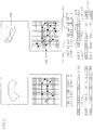
- FIG. 5 is an illustration depicting two examples of touch paths and corresponding mask overlays for a row of pixels.
- the first example of the touch path (on the left of FIG. 5 ) is described above with respect to FIGS. 4A and 4B .
- a second example may be a touch path 359 that is a continuation of the touch path of the first example.
- the touch path 359 crosses itself. Because the touch path 359 crosses itself, start edges 355a of different polygons 327 may occupy a same pixel 341 in the row 339. To cover such a situation, an edge identifier of a related art device would have to calculate additional special processes, thereby requiring additional computing power.
- the above described embodiments are able to cover the present situation with less computing power, even when the touch path 359 is relatively complicated and overlaps itself, because the described embodiments analyze a set of polygons, as opposed to analyzing an entirety of an image representing the touch path. Accordingly, embodiments of the present invention are able to give consistent processing independent from image complexity.
- the eighth pixel of the row 339 corresponds to two start column offsets 353a. Accordingly, the eighth bin offset 350 of the list of bin offset values 352 generated by the histogram module 348 has a value of "2" stored therein (e.g., two polygons 327 both have a start edge 355a at the eighth pixel).
- the accumulator and pixel-fill module 354 will determine that the accumulator values 356 following the eighth accumulator value 356 will be greater than zero until two values corresponding to two stop column offsets 353b are counted (e.g., until two values of "-1" occur in the list of bin offset values 352 without the occurrence of a value of "1"). Accordingly, the mask overlay 335 generated by the accumulator and pixel-fill module 354 will recognize that every pixel from the eighth pixel to a pixel corresponding to the second stop column offset 353b (e.g., the sixteenth pixel) corresponds to the displayed line 100.
- the second stop column offset 353b e.g., the sixteenth pixel
- FIG. 6 is a flow chart illustrating a mask overlay generation process according to an embodiment of the present invention.
- touch path data including a set of interpolated time-stamped touch points corresponding to a touch path is received (e.g., received at the line width module 342 or the LUT generator 331 from the touch path logic module 330).
- a line width setting is received (e.g., received at the line width module 342 or the LUT generator 331 from software or the AP 202).
- one or more touch path vectors corresponding to paths between adjacent ones of the interpolated time-stamped touch points are generated (e.g., touch path vectors 321 generated by the line width module 342 or the LUT generator 331).
- zero or more vertex points of a vertex array corresponding to the interpolated time-stamped touch points, the touch path vectors, and the line width setting are generated (e.g., vertex points 324 generated by the line width module 342 or the LUT generator 331).
- one or more polygons are generated for each set of four vertex points to define edges of a line segment of a given width based on the vertex points and the line width setting (e.g., polygons 327 generated by the line width module 342 or the LUT generator 331).
- intersection points are determined for each row of pixels that intersect zero or more edges of the polygons based on the vertex points (e.g., intersection points 353a, 353b for an eleventh row 339 of pixels 341 determined by the interpolation calculator 336, or zero intersection points for a first row 339 of pixels 341 that is entirely outside of the touch path).
- start edges and stop edges of each of the polygons based on the intersection points are determined (e.g., start edges 355a and stop edges 355b determined by the interpolation calculator 336).
- start column offsets and stop column offsets are generated for each row of pixels based on the start edges and the stop edges (e.g., start column offsets 353a and stop column offsets 353b determined by the interpolation calculator 336).
- a bin offset value for the current row is generated for each row of pixels indicating the start edges and the stop edges by incrementing a corresponding bin offset by one for each start column offset, and by decrementing a corresponding subsequent bin offset by one for each stop column offset (e.g., list of bin offset values 352 generated by the histogram module 348).
- an accumulator value corresponding to each of the pixels of each row is generated by initializing a count to 0, by iterating each bin offset, and by adding to or subtracting from the previous count based on the bin offsets (e.g., accumulator values 356 generated by the accumulator and pixel-fill module 354 by iterating each bin offset 350 of the list of bin offset values 352).
- accumulator values 356 generated by the accumulator and pixel-fill module 354 by iterating each bin offset 350 of the list of bin offset values 352.
- whether each of the accumulator values is greater than zero or equal to zero is determined (e.g., determined by the accumulator and pixel-fill module 354).
- a mask overlay is generated by generating a "1" of a one bit enable signal in the mask overlay for each accumulator value that is greater than zero to indicate that the corresponding pixel corresponds to an edge or an interior of a polygon, and by generating a "0" of the one bit enable signal in the mask overlay for each accumulator value that is equal to zero (e.g., mask overlay 335 generated by the accumulator and pixel-fill module 354).
- the above described embodiments of the present invention are able to provide a simple but effective solution that reduces the latency between a touch event and a display response to this touch event.
Landscapes
- Engineering & Computer Science (AREA)
- Theoretical Computer Science (AREA)
- General Engineering & Computer Science (AREA)
- Physics & Mathematics (AREA)
- General Physics & Mathematics (AREA)
- Human Computer Interaction (AREA)
- Computer Networks & Wireless Communication (AREA)
- Controls And Circuits For Display Device (AREA)
Claims (19)
- Verfahren zur Bereitstellung einer visuellen Rückmeldung für ein Anzeigefeld (322) entsprechend einem Berührungsweg (359) auf einem berührungssensitiven Bildschirm, wobei das Verfahren umfasst:Erzeugen (s605) eines Polygons (327) entsprechend einem Scheitel-Array (325), das Kanten des Berührungsweges (359) bestimmt;Bestimmen (s607) von Startkanten (355a) und Stoppkanten (355b) des Polygons (327) für eine Reihe von Pixeln (341);Erzeugen (s609) von Bin-Offsets, die Werte umfassen, die den Startkanten (355a) und den Stoppkanten (355b) entsprechen;Erzeugen (s610) eines Akkumulatorwertes (356) entsprechend jedem der Pixel (341) auf der Grundlage der Bin-Offsets (350), wobei das Erzeugen (s610) des Akkumulatorwertes (356) umfasst:Initialisieren einer Zählung;Wiederholen jedes Bin-Offsets (350) in der Reihenfolge;Addieren zu dem Zählwert für Bin-Offset-Werte, die Startkanten (355a) entsprechen, und Subtrahieren von dem Zählwert für Bin-Offset-Werte, die Stoppkanten (355b) entsprechen; undEingeben des Zählwertes als den Akkumulatorwert (356) entsprechend dem wiederholten Bin-Offset (350);Erzeugen (s612) eines Masken-Overlays (335), das Bits umfasst, die Werte aufweisen, die dadurch bestimmt werden, ob ein jeweiliger Akkumulatorwert der Akkumulatorwerte (356) größer als Null ist; undÜberlagern eines Bildes mit dem Masken-Overlay (335) vor der Wiedergabe eines Bildes durch einen Anwendungsprozessor auf der Grundlage des Berührungsweges (359).
- Verfahren nach Anspruch 1, wobei das Scheitel-Array (325) Scheitelpunkte (324) umfasst, die Berührungspunkten (315) des Berührungsweges (359) entsprechen.
- Verfahren nach Anspruch 2, ferner umfassend das Empfangen (s602) einer Linienbreiteneinstellung (317),
wobei die Scheitelpunkte (324) ferner der Linienbreiteneinstellung (317) entsprechen. - Verfahren nach Anspruch 2 oder 3, umfassend das Empfangen (s601) von Berührungswegdaten, die Berührungspunkte (315) umfassen, die dem Berührungsweg (359) entsprechen.
- Verfahren nach Anspruch 4, wobei die Daten des Berührungsweges (359) ferner Druckdaten umfassen, die dem Berührungsweg (359) entsprechen, und
wobei die Scheitelpunkte (324) des Scheitel-Arrays (325) ferner den Druckdaten entsprechen. - Verfahren nach Anspruch 4 oder 5, ferner umfassend das Erzeugen (s603) eines Berührungswegvektors (321), der einem Weg zwischen benachbarten Berührungspunkten der Berührungspunkte (315) entspricht,
wobei die Scheitelpunkte (324) ferner dem Berührungswegvektor (321) entsprechen. - Verfahren nach einem der vorangehenden Ansprüche, wobei das Erzeugen (s612) des Masken-Overlays (335) umfasst:Erzeugen (s612) einer "1" eines Einbit-Freigabesignals in dem Masken-Overlay (335) für jeden der Akkumulatorwerte (356), der größer als Null ist, um anzugeben, dass die entsprechenden Pixel der Pixel (341) einer Kante oder einem Inneren des Polygons (327) entsprechen; undErzeugen (s612) einer "0" des Einbit-Freigabesignals in dem Masken-Overlay (335) für jeden der Akkumulatorwerte (356), der gleich Null ist.
- Verfahren nach einem der vorangehenden Ansprüche, ferner umfassend das Anzeigen, auf einem Anzeigefeld (322), eines angezeigten Berührungsweges entsprechend dem erzeugten Masken-Overlay (335).
- Verfahren nach einem der vorangehenden Ansprüche, wobei eine Zahl der Pixel (341) in der Reihe (339) von Pixeln (341), eine Zahl der Bin-Offsets (350) in der Liste von Bin-Offset-Werten (352) und eine Zahl der Bits in dem Masken-Overlay (335) gleich sind.
- Verfahren nach einem der vorangehenden Ansprüche, umfassend das Erhöhen (s609) eines entsprechenden Bin-Offsets (350) um 1 für jede der Startkanten (355a) und das Erniedrigen eines entsprechenden nachfolgenden Bin-Offsets (350) um 1 für jede der Stoppkanten (355b), um die Bin-Offsets (350) zu erzeugen.
- System (310) zur Bereitstellung einer visuellen Rückmeldung für ein Anzeigefeld (322) entsprechend einem Berührungsweg (359) auf einem berührungssensitiven Bildschirm, wobei das System (310) umfasst:ein Steuerlogikmodul (333), das so konfiguriert ist, dass es ein Scheitel-Array (325), das Scheitelpunkte (324) umfasst, empfängt, und so konfiguriert ist, dass es ein Masken-Overlay (335) auf der Grundlage des Scheitel-Arrays (325) erzeugt,wobei das Steuerlogikmodul (333) umfasst:einen Interpolationsrechner (336), der so konfiguriert ist, dass er ein oder mehr Polygon/e (327), das/die Kanten des Berührungsweges bestimmt/bestimmen, auf der Grundlage der Scheitelpunkte (324) bestimmt, und so konfiguriert ist, dass er Startspalten-Offsets (353a) und Stoppspalten-Offsets (353b) erzeugt, die Startkanten (355a) bzw. Stoppkanten (355b) des einen oder der mehreren Polygons/Polygone (327) in einer Reihe (339) von Pixeln (341) entsprechen;ein Histogrammmodul (348), das so konfiguriert ist, dass es die Start- und Stoppspalten-Offsets (353a, 353b) empfängt, und so konfiguriert ist, dass es eine Liste von Bin-Offset-Werten (352) auf der Grundlage der Start- und Stoppspalten-Offsets (353a, 353b) erzeugt; undein Akkumulator- und Pixelfüllmodul (354), das so konfiguriert ist, dass es die Liste von Bin-Offset-Werten (352) empfängt, so konfiguriert ist, dass es einen Akkumulatorwert (356) für jedes Pixel (341) der Reihe (339) der Pixel (341) auf der Grundlage der Liste von Bin-Offset-Werten (352) erzeugt, und so konfiguriert ist, dass es ein Masken-Overlay (335) auf der Grundlage der Akkumulatorwerte (356) erzeugt;wobei der Akkumulatorwert (356) erzeugt wird durch:Initialisieren einer Zählung;Wiederholen jedes Bin-Offsets in der Reihenfolge;Addieren zu oder Subtrahieren von dem Zählwert auf der Grundlage der Bin-Offsets; undEingeben des Zählwertes als den Akkumulatorwert (356) entsprechend dem wiederholten Bin-Offset; undwobei das System (310) ferner eine Anzeigetreiber-Schnittstellen-Steuereinrichtung (204) umfasst, die so angeordnet ist, dass sie ein Bild mit dem Masken-Overlay (335) vor der Wiedergabe eines Bildes durch einen Anwendungsprozessor auf der Grundlage des Berührungsweges (359) überlagert.
- System (310) nach Anspruch 11, ferner umfassend einen LUT-Generator (331) (LUT = Lookup Table (Nachschlagetabelle)), der so konfiguriert ist, dass er interpolierte Berührungspunkte (315) entsprechend dem Berührungsweg (359) empfängt, und so konfiguriert ist, dass er das Scheitel-Array (325) auf der Grundlage der interpolierten Berührungspunkte (315) erzeugt.
- System (310) nach Anspruch 12, ferner umfassend ein LUT-Speichermodul (332), das so konfiguriert ist, dass es das Scheitel-Array (325) aus dem LUT-Generator (331) empfängt und speichert, und so konfiguriert ist, dass es das Scheitel-Array (325) an das Steuerlogikmodul (333) ausgibt.
- System (310) nach Anspruch 12 oder 13, wobei der LUT-Generator (331) ein Linienbreitenmodul (342) umfasst.
- System (310) nach Anspruch 12 oder 13, wobei der LUT-Generator (331) ferner so konfiguriert ist, dass er eine Linienbreiteneinstellung (317) empfängt und das Scheitel-Array (325) auf der Grundlage der Linienbreiteneinstellung (317) erzeugt.
- System (310) nach Anspruch 15, wobei der LUT-Generator (331) ferner so konfiguriert ist, dass er einen oder mehr Vektor/en (321) entsprechend dem Berührungsweg (359) bestimmt und das Scheitel-Array (325) auf der Grundlage des einen oder der mehreren Vektors/Vektoren (321) und auf der Grundlage der Linienbreiteneinstellung (317) erzeugt.
- System (310) nach Anspruch 11, wobei die Liste von Bin-Offset-Werten (352) eine Mehrzahl von Bin-Offsets (350) umfasst, von denen jedes einen Wert umfasst, der einem jeweiligen Spalten-Offset entspricht.
- System (310) nach Anspruch 11, wobei die Liste von Bin-Offset-Werten (352) eine Zahl von Bins umfasst, die gleich einer Zahl der Pixel (341) in der Reihe (339) ist.
- System (310) nach Anspruch 18, wobei jedes der Bins einen n-Bit-Speicher zum Speichern eines Wertes entsprechend einem der Pixel (341) an einem Kantenschnittpunkt umfasst.
Applications Claiming Priority (2)
| Application Number | Priority Date | Filing Date | Title |
|---|---|---|---|
| US201562154015P | 2015-04-28 | 2015-04-28 | |
| US14/994,104 US9804709B2 (en) | 2015-04-28 | 2016-01-12 | Vector fill segment method and apparatus to reduce display latency of touch events |
Publications (2)
| Publication Number | Publication Date |
|---|---|
| EP3089004A1 EP3089004A1 (de) | 2016-11-02 |
| EP3089004B1 true EP3089004B1 (de) | 2018-03-21 |
Family
ID=55952972
Family Applications (1)
| Application Number | Title | Priority Date | Filing Date |
|---|---|---|---|
| EP16167584.8A Active EP3089004B1 (de) | 2015-04-28 | 2016-04-28 | Vektorfüllsegmentverfahren und -vorrichtung zur reduzierung der anzeigelatenz von berührungsereignissen |
Country Status (4)
| Country | Link |
|---|---|
| US (1) | US9804709B2 (de) |
| EP (1) | EP3089004B1 (de) |
| KR (1) | KR102304891B1 (de) |
| CN (1) | CN106095155B (de) |
Families Citing this family (8)
| Publication number | Priority date | Publication date | Assignee | Title |
|---|---|---|---|---|
| US10521937B2 (en) * | 2017-02-28 | 2019-12-31 | Corel Corporation | Vector graphics based live sketching methods and systems |
| TWI635441B (zh) * | 2017-06-29 | 2018-09-11 | 宏碁股份有限公司 | 行動裝置及其觸控畫面更新方法 |
| KR102469722B1 (ko) * | 2018-09-21 | 2022-11-22 | 삼성전자주식회사 | 디스플레이 장치 및 그 제어 방법 |
| CN111583147B (zh) * | 2020-05-06 | 2023-06-06 | 北京字节跳动网络技术有限公司 | 图像处理方法、装置、设备及计算机可读存储介质 |
| KR102805922B1 (ko) | 2020-05-11 | 2025-05-12 | 삼성전자주식회사 | 빠른 터치 반응성을 가지는 터치 및 디스플레이 제어 장치, 이를 포함하는 디스플레이 장치 및 이의 구동 방법 |
| CN114385025B (zh) * | 2020-10-22 | 2024-05-07 | 青岛海信商用显示股份有限公司 | 触摸定位方法、装置、设备和存储介质 |
| CN115953505A (zh) * | 2022-12-28 | 2023-04-11 | 深圳创维-Rgb电子有限公司 | 绘画延时优化方法、装置、显示设备及可读存储介质 |
| CN116069187B (zh) * | 2023-01-28 | 2023-09-01 | 荣耀终端有限公司 | 一种显示方法及电子设备 |
Family Cites Families (25)
| Publication number | Priority date | Publication date | Assignee | Title |
|---|---|---|---|---|
| US5694535A (en) | 1995-03-24 | 1997-12-02 | Novell, Inc. | Direct interactive, constant-time curve apparatus and method |
| JP2000517445A (ja) * | 1996-08-28 | 2000-12-26 | ヴィーア・インコーポレイテッド | タッチ画面装置及び方法 |
| AU2680699A (en) | 1998-02-17 | 1999-08-30 | Sun Microsystems, Inc. | Estimating graphics system performance for polygons |
| WO2003096378A2 (en) * | 2002-05-10 | 2003-11-20 | Nec Electronics Corporation | Display driver ic, display module and electrical device incorporating a graphics engine |
| US7652677B2 (en) * | 2006-08-03 | 2010-01-26 | Qualcomm Incorporated | Graphics system employing pixel mask |
| US9189875B2 (en) | 2007-08-06 | 2015-11-17 | Apple Inc. | Advanced import/export panel notifications using a presentation application |
| JP4400667B2 (ja) | 2007-10-04 | 2010-01-20 | セイコーエプソン株式会社 | 描画装置、画像出力装置及びプログラム |
| JP4937359B2 (ja) | 2008-01-15 | 2012-05-23 | 三菱電機株式会社 | 図形描画装置及び図形描画方法 |
| EP2090971B1 (de) * | 2008-02-13 | 2012-06-27 | Research In Motion Limited | Dreidimensionale berührungsempfindliche Anzeigevorrichtung |
| CN101764941B (zh) * | 2008-11-04 | 2013-02-20 | 新奥特(北京)视频技术有限公司 | 一种像素空间掩码矩阵的像素类型的确定方法 |
| CN102414649B (zh) * | 2009-04-30 | 2015-05-20 | 辛纳普蒂克斯公司 | 按照多个规则集合来操作触摸屏控制系统 |
| KR101126167B1 (ko) * | 2010-06-07 | 2012-03-22 | 삼성전자주식회사 | 터치 스크린 및 디스플레이 방법 |
| US8847961B2 (en) * | 2010-06-14 | 2014-09-30 | Microsoft Corporation | Geometry, speed, pressure, and anti-aliasing for ink rendering |
| US9965094B2 (en) | 2011-01-24 | 2018-05-08 | Microsoft Technology Licensing, Llc | Contact geometry tests |
| KR101516339B1 (ko) * | 2011-01-31 | 2015-05-04 | 베이징 에레네벤 인포메이션 테크놀로지 씨오., 엘티디. | 오리지널 수기 필적의 구현 방법과 구현장치 및 전자장치 |
| TW201329821A (zh) | 2011-09-27 | 2013-07-16 | Flatfrog Lab Ab | 用於觸控決定的影像重建技術 |
| US9250794B2 (en) | 2012-01-23 | 2016-02-02 | Victor Manuel SUAREZ ROVERE | Method and apparatus for time-varying tomographic touch imaging and interactive system using same |
| US20130265239A1 (en) * | 2012-04-05 | 2013-10-10 | Research In Motion Limited | Electronic device and method of controlling display of information on a touch-sensitive display |
| AU2012202651A1 (en) * | 2012-05-04 | 2013-11-21 | Canon Kabushiki Kaisha | A method for stroking paths |
| JP2014203351A (ja) * | 2013-04-08 | 2014-10-27 | 船井電機株式会社 | 描画装置、描画方法、及び描画プログラム |
| US9383840B2 (en) * | 2013-04-22 | 2016-07-05 | Samsung Display Co., Ltd. | Method and apparatus to reduce display lag using image overlay |
| US9483176B2 (en) * | 2013-07-08 | 2016-11-01 | Samsung Display Co., Ltd. | Method and apparatus to reduce display lag of soft keyboard presses |
| US9529525B2 (en) | 2013-08-30 | 2016-12-27 | Nvidia Corporation | Methods and apparatus for reducing perceived pen-to-ink latency on touchpad devices |
| US9298299B2 (en) | 2013-10-02 | 2016-03-29 | Synaptics Incorporated | Multi-sensor touch integrated display driver configuration for capacitive sensing devices |
| US9710098B2 (en) * | 2014-03-31 | 2017-07-18 | Samsung Display Co., Ltd. | Method and apparatus to reduce latency of touch events |
-
2016
- 2016-01-12 US US14/994,104 patent/US9804709B2/en active Active
- 2016-04-28 CN CN201610274208.1A patent/CN106095155B/zh active Active
- 2016-04-28 EP EP16167584.8A patent/EP3089004B1/de active Active
- 2016-04-28 KR KR1020160052470A patent/KR102304891B1/ko active Active
Non-Patent Citations (1)
| Title |
|---|
| None * |
Also Published As
| Publication number | Publication date |
|---|---|
| CN106095155A (zh) | 2016-11-09 |
| CN106095155B (zh) | 2021-02-05 |
| US9804709B2 (en) | 2017-10-31 |
| US20160320912A1 (en) | 2016-11-03 |
| EP3089004A1 (de) | 2016-11-02 |
| KR20160128926A (ko) | 2016-11-08 |
| KR102304891B1 (ko) | 2021-09-24 |
Similar Documents
| Publication | Publication Date | Title |
|---|---|---|
| US9804709B2 (en) | Vector fill segment method and apparatus to reduce display latency of touch events | |
| TWI611354B (zh) | 使用圖像重疊減少顯示延遲的系統及方法,以及用於提供回應顯示裝置上所畫路徑之回饋的加速器 | |
| EP2927794B1 (de) | Verfahren und vorrichtung zur reduzierung der latenz von berührungsereignissen | |
| US10110832B2 (en) | Method and apparatus to reduce display lag using scaling | |
| US10127700B2 (en) | Generation of display overlay parameters utilizing touch inputs | |
| US9697803B2 (en) | Method and apparatus to reduce display latency of touch events using image replications | |
| US9811301B2 (en) | Terminal and apparatus and method for reducing display lag | |
| US9851835B2 (en) | Image display system | |
| US11422653B2 (en) | Touch and display control device with fast touch responsiveness, display device including the same, method of operating the same and electronic system including the same | |
| KR102161745B1 (ko) | 터치 입력에 시각적 피드백을 제공하는 가속기, 터치 입력에 시각적 피드백을 제공하는 터치 입력 프로세싱 디바이스 및 방법 | |
| US20160216839A1 (en) | Display device and electronic device including the same | |
| CN114202603B (zh) | 界面图形调整方法、电子设备、存储介质及显示系统 | |
| KR102166684B1 (ko) | 터치처리장치 및 이를 구비하는 디스플레이 기기 | |
| CN118377561A (zh) | 显示方法、装置、系统、电子设备 | |
| CN119917011A (zh) | 书写笔迹的显示方法、交互平板及存储介质 |
Legal Events
| Date | Code | Title | Description |
|---|---|---|---|
| PUAI | Public reference made under article 153(3) epc to a published international application that has entered the european phase |
Free format text: ORIGINAL CODE: 0009012 |
|
| AK | Designated contracting states |
Kind code of ref document: A1 Designated state(s): AL AT BE BG CH CY CZ DE DK EE ES FI FR GB GR HR HU IE IS IT LI LT LU LV MC MK MT NL NO PL PT RO RS SE SI SK SM TR |
|
| AX | Request for extension of the european patent |
Extension state: BA ME |
|
| 17P | Request for examination filed |
Effective date: 20170420 |
|
| RBV | Designated contracting states (corrected) |
Designated state(s): AL AT BE BG CH CY CZ DE DK EE ES FI FR GB GR HR HU IE IS IT LI LT LU LV MC MK MT NL NO PL PT RO RS SE SI SK SM TR |
|
| GRAP | Despatch of communication of intention to grant a patent |
Free format text: ORIGINAL CODE: EPIDOSNIGR1 |
|
| INTG | Intention to grant announced |
Effective date: 20171005 |
|
| GRAS | Grant fee paid |
Free format text: ORIGINAL CODE: EPIDOSNIGR3 |
|
| GRAA | (expected) grant |
Free format text: ORIGINAL CODE: 0009210 |
|
| AK | Designated contracting states |
Kind code of ref document: B1 Designated state(s): AL AT BE BG CH CY CZ DE DK EE ES FI FR GB GR HR HU IE IS IT LI LT LU LV MC MK MT NL NO PL PT RO RS SE SI SK SM TR |
|
| REG | Reference to a national code |
Ref country code: GB Ref legal event code: FG4D |
|
| REG | Reference to a national code |
Ref country code: CH Ref legal event code: EP |
|
| REG | Reference to a national code |
Ref country code: AT Ref legal event code: REF Ref document number: 981773 Country of ref document: AT Kind code of ref document: T Effective date: 20180415 |
|
| REG | Reference to a national code |
Ref country code: IE Ref legal event code: FG4D |
|
| REG | Reference to a national code |
Ref country code: DE Ref legal event code: R096 Ref document number: 602016002085 Country of ref document: DE |
|
| REG | Reference to a national code |
Ref country code: FR Ref legal event code: PLFP Year of fee payment: 3 |
|
| REG | Reference to a national code |
Ref country code: NL Ref legal event code: MP Effective date: 20180321 |
|
| PG25 | Lapsed in a contracting state [announced via postgrant information from national office to epo] |
Ref country code: FI Free format text: LAPSE BECAUSE OF FAILURE TO SUBMIT A TRANSLATION OF THE DESCRIPTION OR TO PAY THE FEE WITHIN THE PRESCRIBED TIME-LIMIT Effective date: 20180321 Ref country code: CY Free format text: LAPSE BECAUSE OF FAILURE TO SUBMIT A TRANSLATION OF THE DESCRIPTION OR TO PAY THE FEE WITHIN THE PRESCRIBED TIME-LIMIT Effective date: 20180321 Ref country code: NO Free format text: LAPSE BECAUSE OF FAILURE TO SUBMIT A TRANSLATION OF THE DESCRIPTION OR TO PAY THE FEE WITHIN THE PRESCRIBED TIME-LIMIT Effective date: 20180621 Ref country code: HR Free format text: LAPSE BECAUSE OF FAILURE TO SUBMIT A TRANSLATION OF THE DESCRIPTION OR TO PAY THE FEE WITHIN THE PRESCRIBED TIME-LIMIT Effective date: 20180321 Ref country code: LT Free format text: LAPSE BECAUSE OF FAILURE TO SUBMIT A TRANSLATION OF THE DESCRIPTION OR TO PAY THE FEE WITHIN THE PRESCRIBED TIME-LIMIT Effective date: 20180321 |
|
| REG | Reference to a national code |
Ref country code: LT Ref legal event code: MG4D |
|
| REG | Reference to a national code |
Ref country code: AT Ref legal event code: MK05 Ref document number: 981773 Country of ref document: AT Kind code of ref document: T Effective date: 20180321 |
|
| PG25 | Lapsed in a contracting state [announced via postgrant information from national office to epo] |
Ref country code: LV Free format text: LAPSE BECAUSE OF FAILURE TO SUBMIT A TRANSLATION OF THE DESCRIPTION OR TO PAY THE FEE WITHIN THE PRESCRIBED TIME-LIMIT Effective date: 20180321 Ref country code: SE Free format text: LAPSE BECAUSE OF FAILURE TO SUBMIT A TRANSLATION OF THE DESCRIPTION OR TO PAY THE FEE WITHIN THE PRESCRIBED TIME-LIMIT Effective date: 20180321 Ref country code: RS Free format text: LAPSE BECAUSE OF FAILURE TO SUBMIT A TRANSLATION OF THE DESCRIPTION OR TO PAY THE FEE WITHIN THE PRESCRIBED TIME-LIMIT Effective date: 20180321 Ref country code: BG Free format text: LAPSE BECAUSE OF FAILURE TO SUBMIT A TRANSLATION OF THE DESCRIPTION OR TO PAY THE FEE WITHIN THE PRESCRIBED TIME-LIMIT Effective date: 20180621 Ref country code: GR Free format text: LAPSE BECAUSE OF FAILURE TO SUBMIT A TRANSLATION OF THE DESCRIPTION OR TO PAY THE FEE WITHIN THE PRESCRIBED TIME-LIMIT Effective date: 20180622 |
|
| PG25 | Lapsed in a contracting state [announced via postgrant information from national office to epo] |
Ref country code: RO Free format text: LAPSE BECAUSE OF FAILURE TO SUBMIT A TRANSLATION OF THE DESCRIPTION OR TO PAY THE FEE WITHIN THE PRESCRIBED TIME-LIMIT Effective date: 20180321 Ref country code: IT Free format text: LAPSE BECAUSE OF FAILURE TO SUBMIT A TRANSLATION OF THE DESCRIPTION OR TO PAY THE FEE WITHIN THE PRESCRIBED TIME-LIMIT Effective date: 20180321 Ref country code: EE Free format text: LAPSE BECAUSE OF FAILURE TO SUBMIT A TRANSLATION OF THE DESCRIPTION OR TO PAY THE FEE WITHIN THE PRESCRIBED TIME-LIMIT Effective date: 20180321 Ref country code: NL Free format text: LAPSE BECAUSE OF FAILURE TO SUBMIT A TRANSLATION OF THE DESCRIPTION OR TO PAY THE FEE WITHIN THE PRESCRIBED TIME-LIMIT Effective date: 20180321 Ref country code: PL Free format text: LAPSE BECAUSE OF FAILURE TO SUBMIT A TRANSLATION OF THE DESCRIPTION OR TO PAY THE FEE WITHIN THE PRESCRIBED TIME-LIMIT Effective date: 20180321 Ref country code: ES Free format text: LAPSE BECAUSE OF FAILURE TO SUBMIT A TRANSLATION OF THE DESCRIPTION OR TO PAY THE FEE WITHIN THE PRESCRIBED TIME-LIMIT Effective date: 20180321 Ref country code: AL Free format text: LAPSE BECAUSE OF FAILURE TO SUBMIT A TRANSLATION OF THE DESCRIPTION OR TO PAY THE FEE WITHIN THE PRESCRIBED TIME-LIMIT Effective date: 20180321 |
|
| PG25 | Lapsed in a contracting state [announced via postgrant information from national office to epo] |
Ref country code: AT Free format text: LAPSE BECAUSE OF FAILURE TO SUBMIT A TRANSLATION OF THE DESCRIPTION OR TO PAY THE FEE WITHIN THE PRESCRIBED TIME-LIMIT Effective date: 20180321 Ref country code: SM Free format text: LAPSE BECAUSE OF FAILURE TO SUBMIT A TRANSLATION OF THE DESCRIPTION OR TO PAY THE FEE WITHIN THE PRESCRIBED TIME-LIMIT Effective date: 20180321 Ref country code: SK Free format text: LAPSE BECAUSE OF FAILURE TO SUBMIT A TRANSLATION OF THE DESCRIPTION OR TO PAY THE FEE WITHIN THE PRESCRIBED TIME-LIMIT Effective date: 20180321 Ref country code: CZ Free format text: LAPSE BECAUSE OF FAILURE TO SUBMIT A TRANSLATION OF THE DESCRIPTION OR TO PAY THE FEE WITHIN THE PRESCRIBED TIME-LIMIT Effective date: 20180321 |
|
| REG | Reference to a national code |
Ref country code: BE Ref legal event code: MM Effective date: 20180430 |
|
| PG25 | Lapsed in a contracting state [announced via postgrant information from national office to epo] |
Ref country code: PT Free format text: LAPSE BECAUSE OF FAILURE TO SUBMIT A TRANSLATION OF THE DESCRIPTION OR TO PAY THE FEE WITHIN THE PRESCRIBED TIME-LIMIT Effective date: 20180723 |
|
| REG | Reference to a national code |
Ref country code: DE Ref legal event code: R097 Ref document number: 602016002085 Country of ref document: DE |
|
| REG | Reference to a national code |
Ref country code: IE Ref legal event code: MM4A |
|
| PLBE | No opposition filed within time limit |
Free format text: ORIGINAL CODE: 0009261 |
|
| STAA | Information on the status of an ep patent application or granted ep patent |
Free format text: STATUS: NO OPPOSITION FILED WITHIN TIME LIMIT |
|
| PG25 | Lapsed in a contracting state [announced via postgrant information from national office to epo] |
Ref country code: MC Free format text: LAPSE BECAUSE OF FAILURE TO SUBMIT A TRANSLATION OF THE DESCRIPTION OR TO PAY THE FEE WITHIN THE PRESCRIBED TIME-LIMIT Effective date: 20180321 Ref country code: DK Free format text: LAPSE BECAUSE OF FAILURE TO SUBMIT A TRANSLATION OF THE DESCRIPTION OR TO PAY THE FEE WITHIN THE PRESCRIBED TIME-LIMIT Effective date: 20180321 Ref country code: LU Free format text: LAPSE BECAUSE OF NON-PAYMENT OF DUE FEES Effective date: 20180428 |
|
| 26N | No opposition filed |
Effective date: 20190102 |
|
| PG25 | Lapsed in a contracting state [announced via postgrant information from national office to epo] |
Ref country code: BE Free format text: LAPSE BECAUSE OF NON-PAYMENT OF DUE FEES Effective date: 20180430 |
|
| PG25 | Lapsed in a contracting state [announced via postgrant information from national office to epo] |
Ref country code: IE Free format text: LAPSE BECAUSE OF NON-PAYMENT OF DUE FEES Effective date: 20180428 |
|
| PG25 | Lapsed in a contracting state [announced via postgrant information from national office to epo] |
Ref country code: SI Free format text: LAPSE BECAUSE OF FAILURE TO SUBMIT A TRANSLATION OF THE DESCRIPTION OR TO PAY THE FEE WITHIN THE PRESCRIBED TIME-LIMIT Effective date: 20180321 |
|
| REG | Reference to a national code |
Ref country code: CH Ref legal event code: PL |
|
| PG25 | Lapsed in a contracting state [announced via postgrant information from national office to epo] |
Ref country code: CH Free format text: LAPSE BECAUSE OF NON-PAYMENT OF DUE FEES Effective date: 20190430 Ref country code: MT Free format text: LAPSE BECAUSE OF NON-PAYMENT OF DUE FEES Effective date: 20180428 Ref country code: LI Free format text: LAPSE BECAUSE OF NON-PAYMENT OF DUE FEES Effective date: 20190430 |
|
| PG25 | Lapsed in a contracting state [announced via postgrant information from national office to epo] |
Ref country code: TR Free format text: LAPSE BECAUSE OF FAILURE TO SUBMIT A TRANSLATION OF THE DESCRIPTION OR TO PAY THE FEE WITHIN THE PRESCRIBED TIME-LIMIT Effective date: 20180321 |
|
| PG25 | Lapsed in a contracting state [announced via postgrant information from national office to epo] |
Ref country code: MK Free format text: LAPSE BECAUSE OF NON-PAYMENT OF DUE FEES Effective date: 20180321 Ref country code: HU Free format text: LAPSE BECAUSE OF FAILURE TO SUBMIT A TRANSLATION OF THE DESCRIPTION OR TO PAY THE FEE WITHIN THE PRESCRIBED TIME-LIMIT; INVALID AB INITIO Effective date: 20160428 |
|
| PG25 | Lapsed in a contracting state [announced via postgrant information from national office to epo] |
Ref country code: IS Free format text: LAPSE BECAUSE OF FAILURE TO SUBMIT A TRANSLATION OF THE DESCRIPTION OR TO PAY THE FEE WITHIN THE PRESCRIBED TIME-LIMIT Effective date: 20180721 |
|
| P01 | Opt-out of the competence of the unified patent court (upc) registered |
Effective date: 20230516 |
|
| PGFP | Annual fee paid to national office [announced via postgrant information from national office to epo] |
Ref country code: DE Payment date: 20250320 Year of fee payment: 10 |
|
| PGFP | Annual fee paid to national office [announced via postgrant information from national office to epo] |
Ref country code: GB Payment date: 20260324 Year of fee payment: 11 |
|
| PGFP | Annual fee paid to national office [announced via postgrant information from national office to epo] |
Ref country code: FR Payment date: 20260323 Year of fee payment: 11 |