EP3084945B1 - Apparatus and method for zero voltage switching - Google Patents
Apparatus and method for zero voltage switching Download PDFInfo
- Publication number
- EP3084945B1 EP3084945B1 EP14871890.1A EP14871890A EP3084945B1 EP 3084945 B1 EP3084945 B1 EP 3084945B1 EP 14871890 A EP14871890 A EP 14871890A EP 3084945 B1 EP3084945 B1 EP 3084945B1
- Authority
- EP
- European Patent Office
- Prior art keywords
- switch
- time
- switching cycle
- voltage
- freewheeling
- Prior art date
- Legal status (The legal status is an assumption and is not a legal conclusion. Google has not performed a legal analysis and makes no representation as to the accuracy of the status listed.)
- Active
Links
- 238000000034 method Methods 0.000 title claims description 23
- 238000012937 correction Methods 0.000 claims description 9
- 238000006243 chemical reaction Methods 0.000 claims description 7
- 238000001514 detection method Methods 0.000 claims description 7
- 238000010586 diagram Methods 0.000 description 18
- 230000003044 adaptive effect Effects 0.000 description 10
- 230000008569 process Effects 0.000 description 8
- 230000007704 transition Effects 0.000 description 6
- JMASRVWKEDWRBT-UHFFFAOYSA-N Gallium nitride Chemical compound [Ga]#N JMASRVWKEDWRBT-UHFFFAOYSA-N 0.000 description 3
- XUIMIQQOPSSXEZ-UHFFFAOYSA-N Silicon Chemical compound [Si] XUIMIQQOPSSXEZ-UHFFFAOYSA-N 0.000 description 3
- 239000003990 capacitor Substances 0.000 description 3
- 230000001276 controlling effect Effects 0.000 description 3
- 230000001105 regulatory effect Effects 0.000 description 3
- 229910052710 silicon Inorganic materials 0.000 description 3
- 239000010703 silicon Substances 0.000 description 3
- 230000001360 synchronised effect Effects 0.000 description 3
- 239000000654 additive Substances 0.000 description 2
- 230000000996 additive effect Effects 0.000 description 2
- 230000008901 benefit Effects 0.000 description 2
- 230000008859 change Effects 0.000 description 2
- 230000001934 delay Effects 0.000 description 2
- 239000011159 matrix material Substances 0.000 description 2
- 238000005259 measurement Methods 0.000 description 2
- 230000000116 mitigating effect Effects 0.000 description 2
- 230000009467 reduction Effects 0.000 description 2
- 230000000630 rising effect Effects 0.000 description 2
- 238000005070 sampling Methods 0.000 description 2
- 229910002601 GaN Inorganic materials 0.000 description 1
- 238000013459 approach Methods 0.000 description 1
- 230000003247 decreasing effect Effects 0.000 description 1
- 230000000977 initiatory effect Effects 0.000 description 1
- 238000003780 insertion Methods 0.000 description 1
- 230000037431 insertion Effects 0.000 description 1
- 230000007246 mechanism Effects 0.000 description 1
- 238000012986 modification Methods 0.000 description 1
- 230000004048 modification Effects 0.000 description 1
- 238000011084 recovery Methods 0.000 description 1
- 239000004065 semiconductor Substances 0.000 description 1
Images


Classifications
-
- H—ELECTRICITY
- H02—GENERATION; CONVERSION OR DISTRIBUTION OF ELECTRIC POWER
- H02M—APPARATUS FOR CONVERSION BETWEEN AC AND AC, BETWEEN AC AND DC, OR BETWEEN DC AND DC, AND FOR USE WITH MAINS OR SIMILAR POWER SUPPLY SYSTEMS; CONVERSION OF DC OR AC INPUT POWER INTO SURGE OUTPUT POWER; CONTROL OR REGULATION THEREOF
- H02M1/00—Details of apparatus for conversion
- H02M1/42—Circuits or arrangements for compensating for or adjusting power factor in converters or inverters
- H02M1/4208—Arrangements for improving power factor of AC input
- H02M1/4225—Arrangements for improving power factor of AC input using a non-isolated boost converter
-
- H—ELECTRICITY
- H02—GENERATION; CONVERSION OR DISTRIBUTION OF ELECTRIC POWER
- H02M—APPARATUS FOR CONVERSION BETWEEN AC AND AC, BETWEEN AC AND DC, OR BETWEEN DC AND DC, AND FOR USE WITH MAINS OR SIMILAR POWER SUPPLY SYSTEMS; CONVERSION OF DC OR AC INPUT POWER INTO SURGE OUTPUT POWER; CONTROL OR REGULATION THEREOF
- H02M1/00—Details of apparatus for conversion
- H02M1/42—Circuits or arrangements for compensating for or adjusting power factor in converters or inverters
- H02M1/4208—Arrangements for improving power factor of AC input
-
- H—ELECTRICITY
- H02—GENERATION; CONVERSION OR DISTRIBUTION OF ELECTRIC POWER
- H02M—APPARATUS FOR CONVERSION BETWEEN AC AND AC, BETWEEN AC AND DC, OR BETWEEN DC AND DC, AND FOR USE WITH MAINS OR SIMILAR POWER SUPPLY SYSTEMS; CONVERSION OF DC OR AC INPUT POWER INTO SURGE OUTPUT POWER; CONTROL OR REGULATION THEREOF
- H02M7/00—Conversion of ac power input into dc power output; Conversion of dc power input into ac power output
- H02M7/42—Conversion of dc power input into ac power output without possibility of reversal
- H02M7/44—Conversion of dc power input into ac power output without possibility of reversal by static converters
- H02M7/46—Conversion of dc power input into ac power output without possibility of reversal by static converters using discharge tubes without control electrode or semiconductor devices without control electrode
-
- H—ELECTRICITY
- H02—GENERATION; CONVERSION OR DISTRIBUTION OF ELECTRIC POWER
- H02M—APPARATUS FOR CONVERSION BETWEEN AC AND AC, BETWEEN AC AND DC, OR BETWEEN DC AND DC, AND FOR USE WITH MAINS OR SIMILAR POWER SUPPLY SYSTEMS; CONVERSION OF DC OR AC INPUT POWER INTO SURGE OUTPUT POWER; CONTROL OR REGULATION THEREOF
- H02M1/00—Details of apparatus for conversion
- H02M1/0003—Details of control, feedback or regulation circuits
- H02M1/0012—Control circuits using digital or numerical techniques
-
- H—ELECTRICITY
- H02—GENERATION; CONVERSION OR DISTRIBUTION OF ELECTRIC POWER
- H02M—APPARATUS FOR CONVERSION BETWEEN AC AND AC, BETWEEN AC AND DC, OR BETWEEN DC AND DC, AND FOR USE WITH MAINS OR SIMILAR POWER SUPPLY SYSTEMS; CONVERSION OF DC OR AC INPUT POWER INTO SURGE OUTPUT POWER; CONTROL OR REGULATION THEREOF
- H02M1/00—Details of apparatus for conversion
- H02M1/0048—Circuits or arrangements for reducing losses
- H02M1/0054—Transistor switching losses
- H02M1/0058—Transistor switching losses by employing soft switching techniques, i.e. commutation of transistors when applied voltage is zero or when current flow is zero
-
- Y—GENERAL TAGGING OF NEW TECHNOLOGICAL DEVELOPMENTS; GENERAL TAGGING OF CROSS-SECTIONAL TECHNOLOGIES SPANNING OVER SEVERAL SECTIONS OF THE IPC; TECHNICAL SUBJECTS COVERED BY FORMER USPC CROSS-REFERENCE ART COLLECTIONS [XRACs] AND DIGESTS
- Y02—TECHNOLOGIES OR APPLICATIONS FOR MITIGATION OR ADAPTATION AGAINST CLIMATE CHANGE
- Y02B—CLIMATE CHANGE MITIGATION TECHNOLOGIES RELATED TO BUILDINGS, e.g. HOUSING, HOUSE APPLIANCES OR RELATED END-USER APPLICATIONS
- Y02B70/00—Technologies for an efficient end-user side electric power management and consumption
- Y02B70/10—Technologies improving the efficiency by using switched-mode power supplies [SMPS], i.e. efficient power electronics conversion e.g. power factor correction or reduction of losses in power supplies or efficient standby modes
Definitions
- Power factor correction (PFC) converters are often used as a front-end stage followed by a regulated DC-DC converter, with the PFC stage converting AC input power to provide a DC output voltage.
- Bridgeless PCF converters omit an input rectifier bridge and provide a cost effective and highly efficient power supply solution for many consumer products, such as server and telecom power equipment, set-top boxes, televisions, and displays.
- Totem-pole type PFC circuits operating using transition mode switching provide the potential for high efficiencies, in which one switch operates as an active switch forming a primary current path with a diode or a return circuit MOSFET while a second totem pole switch operates as a freewheeling or synchronous switch, and the roles of the active and freewheeling switches change as the input voltage switches between positive and negative polarities.
- the potential of high efficiency is mitigated by non-zero switching of the active device, where active switch operation when the device voltage is greater than zero leads to switching loss, and extra conduction losses are found when the active device is switched while the device voltage is negative.
- Gallium nitride (GaN) totem pole devices offer certain benefits with respect to high-frequency switching speeds, low on-state resistance (RDSON) and low reverse-recovery charge, which can be employed to improve PFC efficiency.
- RDSON low on-state resistance
- silicon-based MOSFET device types are more common, and improved control techniques and totem pole PFC systems are desired for improved efficiency without additional cost and process complexity associated with use of GaN devices.
- CN102843025 discloses a control circuit used in a PFC circuit.
- US 6,580,255 relates to adaptive gate drivers for zero voltage switching power conversion circuits.
- control techniques and circuitry are presented for bridgeless totem pole power factor correction converters to facilitate active switch zero voltage switching, where a nominal freewheeling switch on-time is determined according to a Volt x Second balance relationship in each switching cycle and is selectively adjusted or offset based on the voltage across the active switch for the next switching cycle.
- the freewheeling switch on-time is increased if the active switch voltage is above a threshold and is decreased for the next switching cycle if the active switch voltage is negative.
- the control apparatus and methods of the disclosure facilitate regulation around zero voltage switching operation, and zero current switching can be facilitated by selectively delaying turn on of the active switch until a negative active switch voltage returns to zero.
- AC input voltage polarity is sensed and used for designating the active and freewheeling switches and for operating any included return circuit switches in each AC input half cycle.
- Certain embodiments provide for selective freewheeling switch on-time adjustment for interleaved multi-phase PFC converters based on sensing of a single-phase active switch voltage.
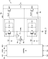
- FIG. 1 shows a bridgeless totem pole power factor correction (PFC) converter or conversion system 2 receiving single-phase AC input power from an AC source 4 and providing a DC output Vo to power a load 6.
- the system 2 includes a controller 8 implementing adaptive zero voltage switching control using selective freewheeling switch on-time adjustment in providing first and second switching control signals 10 and 12 to operate an upper first switch circuit SW1 including transistor Q1 with a body diode D1 and a drain-source capacitance C1, and a second switching circuit SW2 including transistor Q2, body diode D2 and capacitor C2.
- PFC power factor correction
- the transistors Q1 and Q2 are connected in a totem pole circuit with Q1 coupled between a positive DC output terminal or node 5a (VDC+) and a first internal node 3 (VDSHL), and with the second transistor Q2 coupled between the node 3 and a second (negative) DC output node 5b.
- An inductor L is coupled between a first AC input node 4a and the internal node 3, and a return circuit is provided including a first diode D3 with an anode coupled to a second AC input node 4b and a cathode coupled to the first DC output node 5a, along with a second diode D4 having an anode coupled to the lower DC output node 5b (VDC-) and a cathode coupled to the second AC input node 4b.
- FIG. 2 shows another embodiment of the bridgeless totem pole PFC converter system 2 in which the return circuit includes transistors QAC1 and QAC2 replacing the diodes D3 and D4 of FIG. 1 , respectively, where the return circuit transistor components QAC1 and QAC2 are operated according to switching control signals 14 and 16, respectively, from the controller 8 in the embodiment of FIG. 2 .
- the totem pole switches Q1 and Q2 are operated according to higher frequency switching control signals 10 and 12, with the return circuit transistors QAC1 and QAC2 in the embodiment of FIG. 2 being operated by switching control signals 12 and 14 alternating every half cycle of the AC input power.
- Any suitable form of totem pole switches Q1 and Q2 can be used in various embodiments.
- gallium nitride (GaN) N-channel MOSFET transistors are used, although other embodiments are possible using silicon-based MOSFET transistors for the totem pole switches Q1 and Q2.
- the return circuit switches QAC1 and QAC2 can be any suitable form of semiconductor switches, such as silicon-based N-channel MOSFETs as shown in FIG. 2 .
- the controller 8 provides an active high gate control signal 10 (Vg1) to the gate of Q1 and a gate control signal 12 (Vg2) to the gate of Q2, and provides alternating gate control signals 14 and 16 (Vg_ac1 and Vg_ac2) to operate the switches QAC1 and QAC2 of the return circuit in FIG. 2 .
- the controller 8 receives various measurement or feedback signals, including the voltage VDSHL at the intermediate node 3 joining the totem pole switches Q1 and Q2, along with positive and negative voltage signals VDC+ and VDC- representing the voltages at the nodes 5a and 5b, along with one or more feedback signals indicating the AC voltage provided by the source 4 across the nodes or terminals 4a and 4b.
- the controller 8 can regulate the DC output voltage Vo across an output capacitance CO at the output nodes 5a and 5b by the switching operation of Q1 and Q2, and can also ascertain the drain-source voltages across Q1 and Q2 for intelligent switching control to facilitate zero voltage switching as described further below.
- the controller 8 uses the AC input voltage feedback to determine the input polarity for selective switching of any included return circuit transistors QAC 1 and QAC2 (such as FIG. 2 and FIG. 14 below) and for designating a given one of the totem pole switches Q1 and Q2 as an active or main switch and the other as a freewheeling or synchronous switch in each AC input half cycle according to the input voltage polarity.
- the controller 8 designates the lower totem pole switch Q2 as the active switch and the upper totem pole switch Q1 as the freewheeling switch for positive AC input cycles (such as when the voltage across input nodes 4a and 4b is positive), and designates the upper switch Q1 as the active switch and the lower switch Q2 as the freewheeling switch for negative AC input polarities.
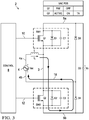
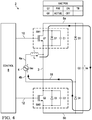
- FIGS. 3-6 show different totem pole switching conditions and corresponding current flow paths for positive and negative AC input cycles for the case shown in FIG. 1 , in which the return circuit includes diodes D3 and D4. Similar switching conditions and flow paths will be found for embodiments using transistors in the return circuit (such as FIGS. 2 and 14 ).
- FIG. 3 shows an example current path 18 (shown by dotted line in the figure) with the totem pole switch Q1 off and Q2 on for a positive polarity half cycle of the AC input source 4, where Q2 is designated as the active switch, and where Q1 is the freewheeling switch.
- the inductor current IL flows through the inductor L from the first AC input node 4a to the first internal node 3 (such as left to right in the figure) and then through the actuated active transistor Q2 to the second DC output node 5b.
- the current continues to flow along the illustrated path 18 through the lower return circuit diode D4 and then to the second AC input node or terminal 4b.
- FIGS. 5 and 6 show the PFC circuit operation for negative AC input half cycles, with Q1 designated as the active switch, and Q2 designated at the freewheeling switch.
- FIG. 5 shows the PFC circuit operation for negative AC input half cycles, with Q1 designated as the active switch, and Q2 designated at the freewheeling switch.
- FIG. 5 shows the PFC circuit operation for negative
- the upper active switch Q1 is turned off, and the freewheeling switch Q2 is turned on, causing the current to flow from the AC input source 4 out of the second AC input node 4b through the diode D3 and the output capacitor CO, returning through the freewheeling transistor Q2 and the inductor L to the first AC input node 4a.
- the controller 8 in one embodiment implements transition mode (TM) operation at the boundary between continuous conduction mode (CCM) and discontinuous conduction mode (DCM), although not a strict requirement of all possible embodiments.
- TM transition mode
- CCM continuous conduction mode
- DCM discontinuous conduction mode
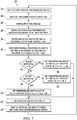
- a method or process 20 is shown in FIG. 7 for controlling a bridgeless totem pole power factor correction converter, such as the converters 2 of FIGS. 1-6 above, where the illustrated controller 8 can be implemented using any suitable logic circuitry, programmable or programmed processor elements, analog circuitry and/or combinations thereof to implement the illustrated process 20 in various embodiments.
- the controller 8 can be a separate power converter control integrated circuit in certain embodiments (such as FIGS. 11 , 12 and 15 below).
- the controller 8 detects positive and negative AC input half cycles based at least partially on the AC input voltage polarity at the nodes 4a and 4b, and designates one of the totem pole switch circuits SW1 or SW2 as an active switch for a given AC input half cycle and designates the other switch circuit as the freewheeling switch for that half cycle.
- the controller 8 designates SW1 (such as Q1) as the active switch and designates SW2 (such as Q2) as the freewheeling switch for negative AC input half cycles, and designates SW2 as the active switch and designates SW1 as the freewheeling switch for positive AC input half cycles.
- the controller 8 operates in a sequence of switching cycles, during which the designated active switch is turned on and then off, followed by the freewheeling switch being turned on and then off.
- the controller 8 provides the first and second switching control signals 10 and 12 to implement these pulses, and may provide dead time control, such that both switches Q1 and Q2 are not turned on at the same time, with certain predefined or adjustable dead times defining non-zero delays between turning one switch off and turning the other switch on, in order to avoid short-circuiting the DC output bus.
- the controller 8 employs constant on-time (COT) switching of the designated active switch for a time Ta determined according to close loop output voltage feedback control, with the designated freewheeling switch being turned on for a freewheeling switch on-time Tb in each switching cycle according to the determination of a Volt x Second relationship.
- COT constant on-time
- Other embodiments are possible in which other pulse width modulation switching techniques are employed by the controller 8 in alternately switching the designated active switch and the designated freewheeling switch, such as duty cycle control.
- the method 20 in FIG. 7 shows one example switching cycle, with the illustrated process flow being repeated in subsequent switching cycles.
- the controller 8 waits for the computed freewheeling switch on-time (Tb) to expire and turns the freewheeling switch off at 22.
- the controller 8 then waits a predetermined (or otherwise computed) second dead time Td2 following turn off of the designated freewheeling switch, and then samples or otherwise senses the voltage Vds across the designated active switch for the given switching cycle at 24, described herein as the current cycle "n".
- Tb computed freewheeling switch on-time
- Td2 second dead time
- the controller 8 receives input signals the DC+, VDSHL and VDC-, and samples the drain-source voltage across Q1 (VDC+ - VDSHL), and the drain-source voltage of Q2 (VDSHL - VDC-).
- the controller 8 also samples the input voltage Vac at 26, and designates the active and freewheeling switches according to the AC input polarity at 28.
- the controller 8 determines the active switch on-time Ta at least partially according to an output voltage control loop.
- any suitable control technique is used by the controller 8 to determine or otherwise compute the active switch on-time Ta, such as current control loops and open loop operation.
- the active switch on-time determined at 30 is then used in the current switching cycle (such as at 46 described below) for operating the designated active switch in the current switching cycle n.
- the controller 8 computes a nominal freewheeling switch on-time Tb_n for the current switching cycle n based at least partially on a Volt x Second balancing relationship using the active switch on-time Ta for the given switching cycle n.
- the controller 8 computes the nominal freewheeling switch on-time Tb_n at 32 for the given switching cycle n as a product of an absolute value of the voltage at the first and second AC input nodes 4a, 4b (
- and the converter output voltage Vo, according to Tb_n (
- the controller 8 selectively offsets or adjusts the nominal freewheeling switch on-time Tb_n for the given switching cycle n, based at least partially on the sampled active switch voltage.
- the controller 8 uses the drain-source voltage Vds across the designated active switch, sampled at 24 to implement selective offsetting or adjustment to provide a computed freewheeling switch on-time Tb_n+1 for the following switching cycle "n+1".
- the controller 8 makes a determination of whether the sampled active switch voltage Vds exceeds a positive threshold TH.
- the controller 8 offsets the nominal freewheeling switch on-time Tb_n for the current switching cycle n by adding a first predetermined offset time ⁇ t1 to the nominal freewheeling switch on-time Tb_n determined at 32, in order to provide a computed freewheeling switch on-time Tb_n+1 for the next switching cycle n+1.
- the controller 8 then turns on the designated active switch for the determined time Ta at 46 and provides the freewheeling switching control signal to actuate the designated freewheeling switch for the computed freewheeling switch on-time Tb_n+1 for the next switching cycle n+1 at 48 and 22 in FIG. 7 .
- the process 20 is then repeated by the controller 8 in a series of consecutive switching cycles.
- the controller 8 can selectively insert dead times between the active in freewheeling switch on-times, such as a first dead time Td1 between the designated active switch being turned off and the designated freewheeling switch being turned on, and a second dead time Td2 between the freewheeling switch being turned off and the active switch being turned on.
- the controller determines at 38 whether the active switch voltage Vds is negative (i.e., Vds ⁇ 0). If not (NO at 38), the ideal zero voltage switching condition has been reached or approximated, because the voltage of the designated active switch is between 0 and the threshold value TH. Accordingly, the controller 8 sets the freewheeling switch on-time Tb_n+1 at 40 to the nominal value computed at 32, and this value is thereafter used at 48 and 22 for operating the freewheeling switch in the next switching cycle "n+1".
- the controller selectively offsets the freewheeling switch on-time in the other direction at 42 by subtracting a second predetermined offset time ⁇ t2 from the nominal freewheeling switch on-time Tb_n to provide the computed freewheeling switch on-time Tb_n+1 for the next switching cycle n+1.
- the first and second offset times ⁇ t1 and ⁇ t2 may be the same, but these may be different in other embodiments.
- the controller 8 in certain embodiments may selectively modify one or both of the offset times ⁇ t1 and ⁇ t2, such as if a condition is reached under which the control operations shown in FIG. 7 result in a certain threshold number of consecutive switching cycles always requiring offsetting in the same direction, in which case the controller 8 may selectively increase the corresponding offset time ⁇ t1 or ⁇ t2.
- the threshold value TH can be modified and adapted based on user input to an integrated circuit controller 8 and/or based on one or more control conditions, such as a certain threshold number of consecutive switching cycles always requiring offsetting in the same direction, in which case the threshold value TH may be selectively reduced.
- the selective offsetting of the computed nominal freewheeling switch on-time advantageously provides a closed loop mechanism for controlling the active switch voltage, thereby mitigating or minimizing both switching loss and conduction loss of the active switch.
- the selective extension of the freewheeling switch on-time at 36 (such as when the sampled active switch voltage Vds is positive) addresses situations where the corresponding drain-source capacitance of the designated active switch is not fully discharged by negative current flow at the time the switch is turned on. Accordingly, this aspect of the process 20 mitigates or avoids switching loss of the active switch.
- the switch Conversely, if the active switch were turned on after the corresponding inductor current IL reverses too much, the switch will suffer from conduction loss due to reverse biasing of the active switch body diode.
- selective subtraction from the computed nominal freewheeling switch on-time at 42 drives the switching operation to more quickly actuate the active switch before the current reversal becomes significant, thereby mitigating such conduction loss.
- the selective freewheeling switch on-time concept regulates the switching by driving operation toward the ideal zero voltage, zero current switching condition for the active switch.
- the designation of the active switch and the freewheeling switch will change depending on the voltage polarity of the AC input, so the control technique of FIG. 7 effectively controls zero voltage switching and mitigates conduction and switching loss for both switches Q1 and Q2 of the totem pole circuitry. In this manner, efficient operation of the bridgeless totem pole PFC converter 2 is facilitated without adding system cost or complexity.
- control concept is applicable with respect to both single phase and interleaved (such as multiphase) PFC architectures, in which freewheeling switch negative current is controlled and mitigated by sensing PFC active switch Vds at or near the turn on point, and the freewheeling switch turn-on time Tb_n+1 is adjusted in the next switching cycle.
- the implementation discussed below in connection with FIGS. 14 and 15 operates with sensing of the active switch voltage for only a single phase, in order to implement the freewheeling switch on-time adjustment for multi-phase totem pole PFC systems.
- the disclosed techniques and control apparatus operate independent of power circuit parameter variations, because the approach involves a regulated configuration adapting to system changes.
- the concepts of the present disclosure may be applied in connection with continuous conduction mode (CCM) and/or discontinuous conduction mode (DCM) or other forms of pulse width modulated switching operation.
- CCM continuous conduction mode
- DCM discontinuous conduction mode
- the concepts of the present disclosure are not limited to use with constant on-time (COT) switching, and can be applied in connection with other forms of pulse width modulated control of a single or multi-phase bridgeless totem pole PFC converter 2.
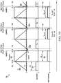
- FIG. 8 shows a waveform diagram 50 of transition mode operation of the PFC converter 2 with constant active switch on-time control for a positive AC input half cycle.
- the absolute AC input voltage waveform 52 (lVac
- FIG. 8 further shows selective actuation of the active switch (such as Q2 in FIG.
- FIG. 9 provides a more detailed waveform diagram 60 of three example switching cycles "n", “n+1” and “n+2", including the active switch drain-source voltage curve 59.
- the adaptive zero voltage switching control in the PFC converter 2 of FIG. 1 adjusts operation from insufficient negative freewheeling current in the illustrated first cycle “n” causing adjustment in the second illustrated cycle "n+1", leading to a regulated zero or near-zero voltage switching situation in the third cycle "n+2".
- the freewheeling pulses 58 are started a first dead time delay time Td1 after the end of the active switch pulses 57, and the active switch pulses 57 are started to begin new switching cycles (such as at 46 in FIG.
- the inductor current IL 56 transitions below zero (i.e., negative) in the first cycle, and without any adjustment in the freewheeling switch on-time Tb_n, the subsequent active switch pulse 57 is started while the active switch has a positive drain-source voltage at 59a above the illustrated non-zero positive threshold level TH.
- the switch voltage at 59b still slightly exceeds the threshold TH as shown in FIG. 9 , and the controller 8 accordingly adds the offset value ⁇ t1 to the subsequent computed nominal freewheeling switch on-time to provide the freewheeling switch on-time for the next cycle "n+2", which further reduces the active switch voltage at 59c in FIG. 9 to be approximately 0, which is the desired operating condition. Accordingly, the operation of selective additive offsetting or adjustment for measured active switch voltages exceeding the threshold advantageously drives the control toward the desired zero voltage switching condition as shown in FIG. 9 .
- FIG. 10 shows adaptive zero voltage switching control in the PFC converter 2 to adjust from excessive negative freewheel current toward zero voltage switching operation. Too much negative current will increase conduction loss if the active switch is turned on while a negative voltage exists across the drain-source connections. To combat this, the process 20 of FIG. 7 samples the active switch drain-source voltage and determines this to be negative in the first illustrated cycle "n" of FIG. 10 . Moreover, at 59d in FIG. 10 , this situation results in the active switch being turned on while the voltage is negative due to negative current preceding the switching, sufficient to provide a reverse charge across the drain-source capacitance of the designated active switch. The controller 8 detects this condition (NO at 34 and YES at 38 in FIG.
- this causes the sampled drain-source voltage of the active switch to be closer to zero in the subsequent cycle "n+1".
- the controller 8 again determines that the active switch drain-source voltage is negative, and accordingly reduces the nominal freewheeling switch on-time by subtracting ⁇ t2 for the next cycle "n+2", thereby driving the active switch drain-source voltage to approximately zero as shown at 59f in FIG. 10 .
- the example embodiment of the controller 8 advantageously delays turning the active switch on until the active switch drain-source voltage is greater than or equal to zero (such as at 44 in FIG. 7 ), as shown by the positive or zero switch Vds voltage starting of the new cycles indicated in FIG. 10 for switching cycles "n+1" and "n+2".
- control method 20 of FIG. 7 and operation of the controller 8 advantageously regulate the switching operation to move operation from either direction toward the optimal zero voltage switching condition. In this manner, both conduction losses and switching losses are mitigated in a dynamic manner independent of system component parameters and other operating conditions, thereby facilitating high efficiency operation, with the Volt x Second nominal freewheeling switch on-time determination (32 in FIG. 7 ) facilitating unity power factor operation of the system 2.
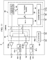
- controller 8 integrated circuit embodiments of the controller 8 are shown for operating the bridgeless PFC converter of FIG. 1 , including driver circuitry 80a and 80b for providing the gate control voltages Vg1 and Vg2 (first and second switching control signals 10 and 12 of FIG. 1 ) to operate the totem pole switches Q1 and Q2, respectively.
- the controller 8 further includes zero voltage switching (ZVS) detection circuitry 81a for sensing or sampling the drain-source voltage across Q1 (such as between VDC+ and VDSHL in FIG. 1 ) and ZVS detection circuitry 81b for sampling the voltage across Q2 (such as between VDSHL and VDC-).
- ZVS zero voltage switching
- An AC detection circuit 82 provides a polarity detection signal 82a to a selection circuit 85 using the AC input voltage (Vac+, Vac-) inputs for AC positive and negative cycle detection and active/main and freewheeling switch determination.
- the Vds of the designated or determined active switch active is detected in each switching cycle by the ZVS circuitry 81, and the result (Vsd greater than, equal to, or less than 0) is used for selectively modifying the predicted freewheeling switch turn-on time Tb for the next cycle, with the active switch turn-on time determined according to a voltage control loop and the nominal freewheeling switch on-time determined using Volt x Second balancing as described above.
- the integrated circuit controller 8 includes dead time control circuitry 88, which may provide inputs for external control of the dead times Td1 and/or Td2, along with a maximum dead time Td_max in certain embodiments.
- the controller 8 further includes a control circuit 89 with a feedback and compensation circuit 83 providing the nominal active switch on-time delay Da to a Volt x Second circuit 84, and additionally provides the on-time Ta as a switchable input to the selection circuit 85 for provision to a driver circuit 80 corresponding to the designated active switch.
- control circuit 89 includes an offsetting or adjustment circuit 86 receiving a nominal freewheeling switch on-time delay Db from the Volt x Second balancing circuit 84, and selectively providing the nominal or adjusted computed freewheeling switch on-time Tb as an input to the selection circuit 85 for provision to the driver circuit 80 corresponding to the designated freewheeling switch.
- FIG. 12 shows further details of one possible embodiment, in which the control circuit 89 includes feedback, compensation and balancing circuitry 83, 84, and the offsetting and dead time circuitry 86, 88 providing the active and freewheeling switch on-times Ta and Tb to a gate signal matrix selection circuit 85.
- the matrix circuit 85 provides inputs to a pulse circuit 87 operative to: provide an active switching pulse signal to the driver circuit 80 to actuate the designated active switch for the active switch on-time Ta for the current cycle; and provide a freewheeling switching pulse signal to the driver circuit 80 to actuate the corresponding designated freewheeling switch for the computed freewheeling switch on-time Tb_n+1 for the next switching cycle, in order to facilitate zero voltage switching of the designated active switch as described above.
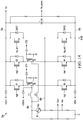
- a waveform diagram 90 shows further operation of the controller 8 in the totem pole PFC converter 2 for three different cases Case 1, Case 2 and Case 3.
- the upper switch Q1 is the designated active switch (such as negative polarity AC half cycle conditions in the illustrated example)
- the corresponding driver circuit 80a and the corresponding zero voltage switching detection circuit 81a provide the turn-on case information including the active switch voltage Vds to the main control circuit 89.
- Case 1 in FIG. 13 shows the active switch turning on at a positive voltage at Vds, in which case the driver circuit 81a sends a single 1us pulse to the control circuit 89 (Encoded Switching information shown in FIG. 13 ).
- the pulse rising edge is synchronized with gate turn-on edge, so the control circuit 89 recognizes that the upper switch Q1 turns on without additional delay insertion, and this edge is used for initiating a new switching cycle in at least one example.
- the driver circuit 80a holds the gate output low until Vds > 0 is detected.
- the gate output pulse is then offset by the dead time delay Td2 and compared with the gate command. In the same way, one single pulse is generated at the gate output turn-on edge, such as 250 ns.
- the control circuit 89 in this embodiment adds a preset time (such as 10 ns) to or reduces the preset time from the freewheeling turn-on time for Case 1 or Case 2, respectively, and no freewheeling switch turn-on time adjustment is needed for Case 3.
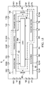
- FIG. 14 shows a 2-phase system 2a having two totem pole circuits including the above-described circuit including Q1 and Q2, along with a second totem pole circuit including totem pole switches Q3 and Q4 also connected between the VDC+ and the VDC- nodes 5a and 5b.
- this embodiment employs MOSFET return circuit transistors QAC1 and QAC2 as described above in connection with FIG. 2 , although diodes may instead be used in other embodiments, such as shown in FIG. 1 above.
- Interleaved multi-phase totem pole PFC circuitry such as the system 2a in FIG.
- the multi-phase system 2a is operated via a controller 8 (such as FIG. 15 ) having corresponding driver output signals to provide gate control signals Vg1-Vg4 to the totem pole circuit switches Q1-Q4, and compensation and output voltage sensing inputs (Comp and Vo_sense inputs and FIG. 15 ) for determining the active switch on-time Ta for voltage regulation or other close loop control of the PFC converter 2a.
- Logic circuit 89a offsets gate signals Q1,2 and Q3,4 by 180 degrees based on detected switching period in previous switching cycle. Multi-phases interleaved control can be implemented by using the same control scheme.
- the example of FIG. 15 includes a frequency control circuit 100 receiving minimum and maximum frequency control inputs (such as f min and f max), and logic circuitry 89a implementing various functions as described above for controlling the driver circuits 80.
- the active switch voltages of only a single phase are needed to implement the selective freewheeling switch on-time adjustment or offsetting concepts as described above, with the controller 8 selectively performing additive offsetting or adjustment of a determined nominal freewheeling switch on-time in a given switching cycle for all phases if the detected or sensed active switch drain-source voltage exceeds a threshold TH or selective subtractive adjustment for all phases if the active switch drain-source voltage is negative.
- the switching cycles of the first and second totem pole circuits may be out of phase with one another (such as phase shifted by 180° in one example), with the controller 8 selectively offsetting the freewheeling switch non-times for the respective totem pole circuits accordingly, based on the measurement of the active switch drain-source voltage for a single one of the totem pole circuits.
- the illustrated PFC converter 2a of FIG. 14 may also include current transformers providing switching circuit current signals or values CT1 and/or CT2 as shown, which may be used by the controller 8 for cycle-by-cycle current limit and/or over current protection, although the current transformers CT may be omitted in certain embodiments.
Description
- Power factor correction (PFC) converters are often used as a front-end stage followed by a regulated DC-DC converter, with the PFC stage converting AC input power to provide a DC output voltage. Bridgeless PCF converters omit an input rectifier bridge and provide a cost effective and highly efficient power supply solution for many consumer products, such as server and telecom power equipment, set-top boxes, televisions, and displays. Totem-pole type PFC circuits operating using transition mode switching provide the potential for high efficiencies, in which one switch operates as an active switch forming a primary current path with a diode or a return circuit MOSFET while a second totem pole switch operates as a freewheeling or synchronous switch, and the roles of the active and freewheeling switches change as the input voltage switches between positive and negative polarities. The potential of high efficiency, however, is mitigated by non-zero switching of the active device, where active switch operation when the device voltage is greater than zero leads to switching loss, and extra conduction losses are found when the active device is switched while the device voltage is negative. Gallium nitride (GaN) totem pole devices offer certain benefits with respect to high-frequency switching speeds, low on-state resistance (RDSON) and low reverse-recovery charge, which can be employed to improve PFC efficiency. However, silicon-based MOSFET device types are more common, and improved control techniques and totem pole PFC systems are desired for improved efficiency without additional cost and process complexity associated with use of GaN devices.
CN102843025 discloses a control circuit used in a PFC circuit.US 6,580,255 relates to adaptive gate drivers for zero voltage switching power conversion circuits. - In described examples, control techniques and circuitry are presented for bridgeless totem pole power factor correction converters to facilitate active switch zero voltage switching, where a nominal freewheeling switch on-time is determined according to a Volt x Second balance relationship in each switching cycle and is selectively adjusted or offset based on the voltage across the active switch for the next switching cycle. The freewheeling switch on-time is increased if the active switch voltage is above a threshold and is decreased for the next switching cycle if the active switch voltage is negative. In this manner, the control apparatus and methods of the disclosure facilitate regulation around zero voltage switching operation, and zero current switching can be facilitated by selectively delaying turn on of the active switch until a negative active switch voltage returns to zero. AC input voltage polarity is sensed and used for designating the active and freewheeling switches and for operating any included return circuit switches in each AC input half cycle. Certain embodiments provide for selective freewheeling switch on-time adjustment for interleaved multi-phase PFC converters based on sensing of a single-phase active switch voltage.
-
-
FIG. 1 is a schematic diagram of a bridgeless totem pole power factor correction (PFC) converter with adaptive zero voltage switching control using adjustable freewheeling switch on-time control. -
FIG. 2 is a schematic diagram of another bridgeless totem pole PFC converter embodiment using MOSFET transistors for half cycle line rectification. -
FIG. 3 is a schematic diagram of current flow in the PFC converter ofFIG. 1 , operating with a positive AC input with the active lower switch on and the upper freewheeling switch off. -
FIG. 4 is a schematic diagram of current flow in the PFC converter ofFIG. 1 , operating with a positive AC input with the active lower switch off and the upper freewheeling switch on. -
FIG. 5 is a schematic diagram of current flow in the PFC converter ofFIG. 1 , operating with a negative AC input with the active upper switch on and the lower freewheeling switch off. -
FIG. 6 is a schematic diagram of current flow in the PFC converter ofFIG. 1 , operating with a negative AC input with the active upper switch off and the lower freewheeling switch on. -
FIG. 7 is a flow diagram of a process implemented in the bridgeless PFC converter controller ofFIG. 1 for adaptive zero voltage switching. -
FIG. 8 is a waveform diagram of transition mode operation with constant active switch on-time control of the PFC converter ofFIG. 1 for a positive AC input half cycle. -
FIG. 9 is a waveform diagram of adaptive zero voltage switching control in the PFC converter ofFIG. 1 to adjust from insufficient negative freewheel current toward zero voltage switching of the active switch. -
FIG. 10 is a waveform diagram of adaptive zero voltage switching control in the PFC converter ofFIG. 1 to adjust from excessive negative freewheel current toward zero voltage switching. -
FIG. 11 is a simplified schematic diagram of a converter control integrated circuit embodiment for operating the bridgeless PFC converter ofFIG. 1 . -
FIG. 12 is a detailed schematic diagram of further details of the converter control integrated circuit embodiment ofFIG. 11 . -
FIG. 13 is a waveform diagram of delay time adjustment for different freewheel switch turn on cases in the adaptive zero voltage switching control of the converter ofFIG. 1 . -
FIG. 14 is a schematic diagram of an interleaved bridgeless totem pole zero voltage switching PFC controller embodiment. -
FIG. 15 is a simplified schematic diagram of another converter control integrated circuit embodiment for operating the interleaved PFC converter ofFIG. 14 . -
FIG. 1 shows a bridgeless totem pole power factor correction (PFC) converter orconversion system 2 receiving single-phase AC input power from anAC source 4 and providing a DC output Vo to power a load 6. Thesystem 2 includes acontroller 8 implementing adaptive zero voltage switching control using selective freewheeling switch on-time adjustment in providing first and secondswitching control signals node 5a (VDC+) and a first internal node 3 (VDSHL), and with the second transistor Q2 coupled between thenode 3 and a second (negative)DC output node 5b. An inductor L is coupled between a firstAC input node 4a and theinternal node 3, and a return circuit is provided including a first diode D3 with an anode coupled to a secondAC input node 4b and a cathode coupled to the firstDC output node 5a, along with a second diode D4 having an anode coupled to the lowerDC output node 5b (VDC-) and a cathode coupled to the secondAC input node 4b. -
FIG. 2 shows another embodiment of the bridgeless totem polePFC converter system 2 in which the return circuit includes transistors QAC1 and QAC2 replacing the diodes D3 and D4 ofFIG. 1 , respectively, where the return circuit transistor components QAC1 and QAC2 are operated according to switchingcontrol signals controller 8 in the embodiment ofFIG. 2 . In at least one example, the totem pole switches Q1 and Q2 are operated according to higher frequencyswitching control signals FIG. 2 being operated by switchingcontrol signals FIG. 2 . Moreover, thecontroller 8 provides an active high gate control signal 10 (Vg1) to the gate of Q1 and a gate control signal 12 (Vg2) to the gate of Q2, and provides alternatinggate control signals 14 and 16 (Vg_ac1 and Vg_ac2) to operate the switches QAC1 and QAC2 of the return circuit inFIG. 2 . - As shown in
FIGS. 1 and2 , thecontroller 8 receives various measurement or feedback signals, including the voltage VDSHL at theintermediate node 3 joining the totem pole switches Q1 and Q2, along with positive and negative voltage signals VDC+ and VDC- representing the voltages at thenodes source 4 across the nodes orterminals controller 8 can regulate the DC output voltage Vo across an output capacitance CO at theoutput nodes controller 8 uses the AC input voltage feedback to determine the input polarity for selective switching of any included returncircuit transistors QAC 1 and QAC2 (such asFIG. 2 andFIG. 14 below) and for designating a given one of the totem pole switches Q1 and Q2 as an active or main switch and the other as a freewheeling or synchronous switch in each AC input half cycle according to the input voltage polarity. - Referring also to
FIGS. 3-6 , thecontroller 8 designates the lower totem pole switch Q2 as the active switch and the upper totem pole switch Q1 as the freewheeling switch for positive AC input cycles (such as when the voltage acrossinput nodes FIGS. 3-6 show different totem pole switching conditions and corresponding current flow paths for positive and negative AC input cycles for the case shown inFIG. 1 , in which the return circuit includes diodes D3 and D4. Similar switching conditions and flow paths will be found for embodiments using transistors in the return circuit (such asFIGS. 2 and14 ). -
FIG. 3 shows an example current path 18 (shown by dotted line in the figure) with the totem pole switch Q1 off and Q2 on for a positive polarity half cycle of theAC input source 4, where Q2 is designated as the active switch, and where Q1 is the freewheeling switch. In this case, the inductor current IL flows through the inductor L from the firstAC input node 4a to the first internal node 3 (such as left to right in the figure) and then through the actuated active transistor Q2 to the secondDC output node 5b. The current continues to flow along the illustratedpath 18 through the lower return circuit diode D4 and then to the second AC input node orterminal 4b. The operation with the active switch Q2 in the on or conductive state ofFIG. 3 increases the current IL through the inductor L. This is followed by the switching state shown inFIG. 4 , also for a positive AC input voltage. InFIG. 4 , the freewheeling totem pole switch Q1 is turned on, and the lower active switch Q2 is turned off, with the current in this case flowing from the inductor L to theinternal node 3 and then through the freewheeling switch Q1 to the upper or firstDC output node 5a. This current flow charges the output capacitor CO and returns from the lower or secondDC output node 5b through the return circuit diode D4 to the negativeAC input terminal 4b as shown inFIG. 4 . -
FIGS. 5 and6 show the PFC circuit operation for negative AC input half cycles, with Q1 designated as the active switch, and Q2 designated at the freewheeling switch. Current flows inFIG. 5 with Q1 on and Q2 off, along thepath 18 from the secondAC input node 4b through the upper return circuit diode D3, returning to the active switch Q1, and building up the reverse current IL through the inductor L from the firstinternal node 3 to the left to return to the firstAC input node 4a. InFIG. 6 , the upper active switch Q1 is turned off, and the freewheeling switch Q2 is turned on, causing the current to flow from theAC input source 4 out of the secondAC input node 4b through the diode D3 and the output capacitor CO, returning through the freewheeling transistor Q2 and the inductor L to the firstAC input node 4a. - Referring also to
FIG. 7 , thecontroller 8 in one embodiment implements transition mode (TM) operation at the boundary between continuous conduction mode (CCM) and discontinuous conduction mode (DCM), although not a strict requirement of all possible embodiments. A method or process 20 is shown inFIG. 7 for controlling a bridgeless totem pole power factor correction converter, such as theconverters 2 ofFIGS. 1-6 above, where the illustratedcontroller 8 can be implemented using any suitable logic circuitry, programmable or programmed processor elements, analog circuitry and/or combinations thereof to implement the illustrated process 20 in various embodiments. Moreover, thecontroller 8 can be a separate power converter control integrated circuit in certain embodiments (such asFIGS. 11 ,12 and15 below). In operation, thecontroller 8 detects positive and negative AC input half cycles based at least partially on the AC input voltage polarity at thenodes controller 8 designates SW1 (such as Q1) as the active switch and designates SW2 (such as Q2) as the freewheeling switch for negative AC input half cycles, and designates SW2 as the active switch and designates SW1 as the freewheeling switch for positive AC input half cycles. - The
controller 8 operates in a sequence of switching cycles, during which the designated active switch is turned on and then off, followed by the freewheeling switch being turned on and then off. In certain embodiments, thecontroller 8 provides the first and secondswitching control signals controller 8 employs constant on-time (COT) switching of the designated active switch for a time Ta determined according to close loop output voltage feedback control, with the designated freewheeling switch being turned on for a freewheeling switch on-time Tb in each switching cycle according to the determination of a Volt x Second relationship. Other embodiments are possible in which other pulse width modulation switching techniques are employed by thecontroller 8 in alternately switching the designated active switch and the designated freewheeling switch, such as duty cycle control. - The method 20 in
FIG. 7 shows one example switching cycle, with the illustrated process flow being repeated in subsequent switching cycles. Beginning with the freewheeling switch on, thecontroller 8 waits for the computed freewheeling switch on-time (Tb) to expire and turns the freewheeling switch off at 22. Thecontroller 8 then waits a predetermined (or otherwise computed) second dead time Td2 following turn off of the designated freewheeling switch, and then samples or otherwise senses the voltage Vds across the designated active switch for the given switching cycle at 24, described herein as the current cycle "n". Moreover, as shown inFIG. 1 , thecontroller 8 receives input signals the DC+, VDSHL and VDC-, and samples the drain-source voltage across Q1 (VDC+ - VDSHL), and the drain-source voltage of Q2 (VDSHL - VDC-). Thecontroller 8 also samples the input voltage Vac at 26, and designates the active and freewheeling switches according to the AC input polarity at 28. - At 30 in
FIG. 7 , thecontroller 8 determines the active switch on-time Ta at least partially according to an output voltage control loop. Other embodiments are possible, in which any suitable control technique is used by thecontroller 8 to determine or otherwise compute the active switch on-time Ta, such as current control loops and open loop operation. The active switch on-time determined at 30 is then used in the current switching cycle (such as at 46 described below) for operating the designated active switch in the current switching cycle n. - At 32 in
FIG. 7 , thecontroller 8 computes a nominal freewheeling switch on-time Tb_n for the current switching cycle n based at least partially on a Volt x Second balancing relationship using the active switch on-time Ta for the given switching cycle n. In one embodiment, thecontroller 8 computes the nominal freewheeling switch on-time Tb_n at 32 for the given switching cycle n as a product of an absolute value of the voltage at the first and secondAC input nodes - At 34-42 in
FIG. 7 , thecontroller 8 selectively offsets or adjusts the nominal freewheeling switch on-time Tb_n for the given switching cycle n, based at least partially on the sampled active switch voltage. In at least one example, thecontroller 8 uses the drain-source voltage Vds across the designated active switch, sampled at 24 to implement selective offsetting or adjustment to provide a computed freewheeling switch on-time Tb_n+1 for the following switching cycle "n+1". At 34 inFIG. 7 , thecontroller 8 makes a determination of whether the sampled active switch voltage Vds exceeds a positive threshold TH. If so (YES at 34), thecontroller 8 offsets the nominal freewheeling switch on-time Tb_n for the current switching cycle n by adding a first predetermined offset time Δt1 to the nominal freewheeling switch on-time Tb_n determined at 32, in order to provide a computed freewheeling switch on-time Tb_n+1 for the next switchingcycle n+ 1. - The
controller 8 then turns on the designated active switch for the determined time Ta at 46 and provides the freewheeling switching control signal to actuate the designated freewheeling switch for the computed freewheeling switch on-time Tb_n+1 for the next switching cycle n+1 at 48 and 22 inFIG. 7 . The process 20 is then repeated by thecontroller 8 in a series of consecutive switching cycles. Moreover, as discussed above, thecontroller 8 can selectively insert dead times between the active in freewheeling switch on-times, such as a first dead time Td1 between the designated active switch being turned off and the designated freewheeling switch being turned on, and a second dead time Td2 between the freewheeling switch being turned off and the active switch being turned on. - If the drain-source voltage of the active switch does not exceed the positive threshold TH (NO at 34 in
FIG. 7 ), the controller determines at 38 whether the active switch voltage Vds is negative (i.e., Vds < 0). If not (NO at 38), the ideal zero voltage switching condition has been reached or approximated, because the voltage of the designated active switch is between 0 and the threshold value TH. Accordingly, thecontroller 8 sets the freewheeling switch on-time Tb_n+ 1 at 40 to the nominal value computed at 32, and this value is thereafter used at 48 and 22 for operating the freewheeling switch in the next switching cycle "n+1". If instead the active switch Vds is negative (YES at 38), then the controller selectively offsets the freewheeling switch on-time in the other direction at 42 by subtracting a second predetermined offset time Δt2 from the nominal freewheeling switch on-time Tb_n to provide the computed freewheeling switch on-time Tb_n+1 for the next switchingcycle n+ 1. - In certain implementations, the first and second offset times Δt1 and Δt2 may be the same, but these may be different in other embodiments. Furthermore, the
controller 8 in certain embodiments may selectively modify one or both of the offset times Δt1 and Δt2, such as if a condition is reached under which the control operations shown inFIG. 7 result in a certain threshold number of consecutive switching cycles always requiring offsetting in the same direction, in which case thecontroller 8 may selectively increase the corresponding offset time Δt1 or Δt2. Moreover, in other possible embodiments, the threshold value TH can be modified and adapted based on user input to anintegrated circuit controller 8 and/or based on one or more control conditions, such as a certain threshold number of consecutive switching cycles always requiring offsetting in the same direction, in which case the threshold value TH may be selectively reduced. - The selective offsetting of the computed nominal freewheeling switch on-time, as shown for example at 34-42 in
FIG. 7 , advantageously provides a closed loop mechanism for controlling the active switch voltage, thereby mitigating or minimizing both switching loss and conduction loss of the active switch. In at least one example, the selective extension of the freewheeling switch on-time at 36 (such as when the sampled active switch voltage Vds is positive) addresses situations where the corresponding drain-source capacitance of the designated active switch is not fully discharged by negative current flow at the time the switch is turned on. Accordingly, this aspect of the process 20 mitigates or avoids switching loss of the active switch. Conversely, if the active switch were turned on after the corresponding inductor current IL reverses too much, the switch will suffer from conduction loss due to reverse biasing of the active switch body diode. For example, selective subtraction from the computed nominal freewheeling switch on-time at 42 drives the switching operation to more quickly actuate the active switch before the current reversal becomes significant, thereby mitigating such conduction loss. Accordingly, in operation, the selective freewheeling switch on-time concept regulates the switching by driving operation toward the ideal zero voltage, zero current switching condition for the active switch. Moreover, the designation of the active switch and the freewheeling switch will change depending on the voltage polarity of the AC input, so the control technique ofFIG. 7 effectively controls zero voltage switching and mitigates conduction and switching loss for both switches Q1 and Q2 of the totem pole circuitry. In this manner, efficient operation of the bridgeless totempole PFC converter 2 is facilitated without adding system cost or complexity. - Accordingly, these techniques provide a reliable control scheme to achieve zero voltage or near-zero voltage switching. Volt x Second balancing is employed in order to set the freewheeling switch nominal on-time value, which is adaptively changed based on the sensed Vds to regulate the system operation toward zero voltage switching. As a result, high power factor operation of the
PFC system 2 can be facilitated by the application of the intelligent adaptive switching control aspects of the present disclosure. Also, the disclosed techniques do not require complicated high-speed current sensing circuitry to achieve zero or near-zero current switching of the active switch. Moreover, as discussed below in connection withFIG. 14 , the control concept is applicable with respect to both single phase and interleaved (such as multiphase) PFC architectures, in which freewheeling switch negative current is controlled and mitigated by sensing PFC active switch Vds at or near the turn on point, and the freewheeling switch turn-ontime Tb_n+ 1 is adjusted in the next switching cycle. Also, the implementation discussed below in connection withFIGS. 14 and15 operates with sensing of the active switch voltage for only a single phase, in order to implement the freewheeling switch on-time adjustment for multi-phase totem pole PFC systems. Furthermore, the disclosed techniques and control apparatus operate independent of power circuit parameter variations, because the approach involves a regulated configuration adapting to system changes. Moreover, while shown and described above in connection with transition mode operation, the concepts of the present disclosure may be applied in connection with continuous conduction mode (CCM) and/or discontinuous conduction mode (DCM) or other forms of pulse width modulated switching operation. Also, the concepts of the present disclosure are not limited to use with constant on-time (COT) switching, and can be applied in connection with other forms of pulse width modulated control of a single or multi-phase bridgeless totempole PFC converter 2. - Referring also to
FIGS. 8-10 ,FIG. 8 shows a waveform diagram 50 of transition mode operation of thePFC converter 2 with constant active switch on-time control for a positive AC input half cycle. In at least one example, the absolute AC input voltage waveform 52 (lVac|∗K) is generally sinusoidal through the illustrated positive half cycle, as is the corresponding AC input current 54, with the inductor current IL shown ascurve 56.FIG. 8 further shows selective actuation of the active switch (such as Q2 inFIG. 1 being active for positive AC input half cycles), with the gate-sourceswitching signal curve 57 representing the gate-source voltage Vgs of the active switch Q2 for a constant on-time of Ta, and selective actuation of the freewheeling switch (Q1 in this example) via gate-source voltage waveform 58. Moreover, as shown inFIG. 8 , the freewheeling switch on-time Tb changes over the course of the AC input positive half cycle, generally in proportion to the absolute value of theAC input voltage 52 based on the Volt x Second relationship in the equation Tb_n = (|Vac| x Ta)/(Vo - |Vac|), where the active switch on-time Ta is generally constant in this example. -
FIG. 9 provides a more detailed waveform diagram 60 of three example switching cycles "n", "n+1" and "n+2", including the active switch drain-source voltage curve 59. As shown inFIG. 9 , the adaptive zero voltage switching control in thePFC converter 2 ofFIG. 1 adjusts operation from insufficient negative freewheeling current in the illustrated first cycle "n" causing adjustment in the second illustrated cycle "n+1", leading to a regulated zero or near-zero voltage switching situation in the third cycle "n+2". Moreover, as shown inFIG. 9 , the freewheelingpulses 58 are started a first dead time delay time Td1 after the end of theactive switch pulses 57, and theactive switch pulses 57 are started to begin new switching cycles (such as at 46 inFIG. 7 above) a second dead time delay Td2 after the freewheeling switch is turned off under control of theconverter controller 8. In at least one example, the inductorcurrent IL 56 transitions below zero (i.e., negative) in the first cycle, and without any adjustment in the freewheeling switch on-time Tb_n, the subsequentactive switch pulse 57 is started while the active switch has a positive drain-source voltage at 59a above the illustrated non-zero positive threshold level TH. - In this case, the negative current is insufficient to fully discharge the main drain-source capacitance of the active switch for the desired zero voltage switching operation. Accordingly, the
controller 8 samples the active switch voltage (such as at 24 inFIG. 7 ) following the freewheeling switch being turned off, and determines that the active switch drain-source voltage (at 59a inFIG. 9 ) exceeds the threshold TH (YES at 34 inFIG. 7 ). Accordingly, thecontroller 8 adds the offset value Δt1 to the nominal freewheeling switch on-time to provide the freewheeling switch on-time for the next cycle "n+1" (Tb_n+1 = Tb_n + Δt1 at 36 inFIG. 7 ). As shown inFIG. 9 , this results in an extension of the freewheeling switch in-time in the next cycle, resulting in a reduction in the sampled active switch drain-source voltage in the next sample at 59b. In at least one example, the switch voltage at 59b still slightly exceeds the threshold TH as shown inFIG. 9 , and thecontroller 8 accordingly adds the offset value Δt1 to the subsequent computed nominal freewheeling switch on-time to provide the freewheeling switch on-time for the next cycle "n+2", which further reduces the active switch voltage at 59c inFIG. 9 to be approximately 0, which is the desired operating condition. Accordingly, the operation of selective additive offsetting or adjustment for measured active switch voltages exceeding the threshold advantageously drives the control toward the desired zero voltage switching condition as shown inFIG. 9 . -
FIG. 10 shows adaptive zero voltage switching control in thePFC converter 2 to adjust from excessive negative freewheel current toward zero voltage switching operation. Too much negative current will increase conduction loss if the active switch is turned on while a negative voltage exists across the drain-source connections. To combat this, the process 20 ofFIG. 7 samples the active switch drain-source voltage and determines this to be negative in the first illustrated cycle "n" ofFIG. 10 . Moreover, at 59d inFIG. 10 , this situation results in the active switch being turned on while the voltage is negative due to negative current preceding the switching, sufficient to provide a reverse charge across the drain-source capacitance of the designated active switch. Thecontroller 8 detects this condition (NO at 34 and YES at 38 inFIG. 7 ), and accordingly reduces the nominal freewheeling switch on-time determined at 32 by Δt2 in order to provide the computed freewheeling switch on-time for the subsequent cycle "n+1" as Tb_n+1 = Tb_n - Δt2 at 42 inFIG. 7 . - As shown at 59e in
FIG. 10 , this causes the sampled drain-source voltage of the active switch to be closer to zero in the subsequent cycle "n+1". For this cycle, thecontroller 8 again determines that the active switch drain-source voltage is negative, and accordingly reduces the nominal freewheeling switch on-time by subtracting Δt2 for the next cycle "n+2", thereby driving the active switch drain-source voltage to approximately zero as shown at 59f inFIG. 10 . Moreover, the example embodiment of thecontroller 8 advantageously delays turning the active switch on until the active switch drain-source voltage is greater than or equal to zero (such as at 44 inFIG. 7 ), as shown by the positive or zero switch Vds voltage starting of the new cycles indicated inFIG. 10 for switching cycles "n+1" and "n+2". This operation provides the additional benefit of facilitating zero current switching in addition to zero voltage switching, which in turn facilitates reduction of electromagnetic interference (EMI) and minimizes active FET's conduction loss. Accordingly, the control method 20 ofFIG. 7 and operation of thecontroller 8 advantageously regulate the switching operation to move operation from either direction toward the optimal zero voltage switching condition. In this manner, both conduction losses and switching losses are mitigated in a dynamic manner independent of system component parameters and other operating conditions, thereby facilitating high efficiency operation, with the Volt x Second nominal freewheeling switch on-time determination (32 inFIG. 7 ) facilitating unity power factor operation of thesystem 2. - Referring now to
FIGS. 11 and12 , integrated circuit embodiments of thecontroller 8 are shown for operating the bridgeless PFC converter ofFIG. 1 , includingdriver circuitry 80a and 80b for providing the gate control voltages Vg1 and Vg2 (first and secondswitching control signals FIG. 1 ) to operate the totem pole switches Q1 and Q2, respectively. Thecontroller 8 further includes zero voltage switching (ZVS)detection circuitry 81a for sensing or sampling the drain-source voltage across Q1 (such as between VDC+ and VDSHL inFIG. 1 ) andZVS detection circuitry 81b for sampling the voltage across Q2 (such as between VDSHL and VDC-). AnAC detection circuit 82 provides apolarity detection signal 82a to aselection circuit 85 using the AC input voltage (Vac+, Vac-) inputs for AC positive and negative cycle detection and active/main and freewheeling switch determination. The Vds of the designated or determined active switch active is detected in each switching cycle by theZVS circuitry 81, and the result (Vsd greater than, equal to, or less than 0) is used for selectively modifying the predicted freewheeling switch turn-on time Tb for the next cycle, with the active switch turn-on time determined according to a voltage control loop and the nominal freewheeling switch on-time determined using Volt x Second balancing as described above. Also, theintegrated circuit controller 8 includes deadtime control circuitry 88, which may provide inputs for external control of the dead times Td1 and/or Td2, along with a maximum dead time Td_max in certain embodiments. Thecontroller 8 further includes acontrol circuit 89 with a feedback andcompensation circuit 83 providing the nominal active switch on-time delay Da to a Voltx Second circuit 84, and additionally provides the on-time Ta as a switchable input to theselection circuit 85 for provision to adriver circuit 80 corresponding to the designated active switch. Also, thecontrol circuit 89 includes an offsetting oradjustment circuit 86 receiving a nominal freewheeling switch on-time delay Db from the Volt xSecond balancing circuit 84, and selectively providing the nominal or adjusted computed freewheeling switch on-time Tb as an input to theselection circuit 85 for provision to thedriver circuit 80 corresponding to the designated freewheeling switch. -
FIG. 12 shows further details of one possible embodiment, in which thecontrol circuit 89 includes feedback, compensation and balancingcircuitry dead time circuitry matrix selection circuit 85. Thematrix circuit 85 provides inputs to apulse circuit 87 operative to: provide an active switching pulse signal to thedriver circuit 80 to actuate the designated active switch for the active switch on-time Ta for the current cycle; and provide a freewheeling switching pulse signal to thedriver circuit 80 to actuate the corresponding designated freewheeling switch for the computed freewheeling switch on-time Tb_n+1 for the next switching cycle, in order to facilitate zero voltage switching of the designated active switch as described above. - Referring also to
FIG. 13 , a waveform diagram 90 shows further operation of thecontroller 8 in the totempole PFC converter 2 for threedifferent cases Case 1,Case 2 andCase 3. For the case in which the upper switch Q1 is the designated active switch (such as negative polarity AC half cycle conditions in the illustrated example), the correspondingdriver circuit 80a and the corresponding zero voltage switchingdetection circuit 81a provide the turn-on case information including the active switch voltage Vds to themain control circuit 89.Case 1 inFIG. 13 shows the active switch turning on at a positive voltage at Vds, in which case thedriver circuit 81a sends a single 1us pulse to the control circuit 89 (Encoded Switching information shown inFIG. 13 ). The pulse rising edge is synchronized with gate turn-on edge, so thecontrol circuit 89 recognizes that the upper switch Q1 turns on without additional delay insertion, and this edge is used for initiating a new switching cycle in at least one example. When a negative voltage is detected inCase 2 at the rising edge of a Q1 turn-on command, thedriver circuit 80a holds the gate output low until Vds > 0 is detected. The gate output pulse is then offset by the dead time delay Td2 and compared with the gate command. In the same way, one single pulse is generated at the gate output turn-on edge, such as 250 ns. When the desired or optimal turning on condition is reached as shown inCase 3, the switching is turned on with Vds = 0, with theupper driver circuit 80a providing thecontrol circuit 89 with three 250 ns pulses in a 1 us period as shown inFIG. 13 . Based on the top driver switching case information, thecontrol circuit 89 in this embodiment adds a preset time (such as 10 ns) to or reduces the preset time from the freewheeling turn-on time forCase 1 orCase 2, respectively, and no freewheeling switch turn-on time adjustment is needed forCase 3. - Referring also to
FIGS. 14 and15 , the concepts of the present disclosure may be employed in control of interleaved bridgeless totem pole zero voltage switching PFC controller embodiments.FIG. 14 shows a 2-phase system 2a having two totem pole circuits including the above-described circuit including Q1 and Q2, along with a second totem pole circuit including totem pole switches Q3 and Q4 also connected between the VDC+ and the VDC-nodes FIG. 2 , although diodes may instead be used in other embodiments, such as shown inFIG. 1 above. Interleaved multi-phase totem pole PFC circuitry, such as thesystem 2a inFIG. 14 , is particularly advantageous for high-power applications (such as 300 Watts or more). As with the above-described single-phase embodiments, themulti-phase system 2a is operated via a controller 8 (such asFIG. 15 ) having corresponding driver output signals to provide gate control signals Vg1-Vg4 to the totem pole circuit switches Q1-Q4, and compensation and output voltage sensing inputs (Comp and Vo_sense inputs andFIG. 15 ) for determining the active switch on-time Ta for voltage regulation or other close loop control of thePFC converter 2a.Logic circuit 89a offsets gate signals Q1,2 and Q3,4 by 180 degrees based on detected switching period in previous switching cycle. Multi-phases interleaved control can be implemented by using the same control scheme. Also, the example ofFIG. 15 includes afrequency control circuit 100 receiving minimum and maximum frequency control inputs (such as f min and f max), andlogic circuitry 89a implementing various functions as described above for controlling thedriver circuits 80. - Moreover, in this example, the active switch voltages of only a single phase (such as Vds of Q1 and Q2) are needed to implement the selective freewheeling switch on-time adjustment or offsetting concepts as described above, with the
controller 8 selectively performing additive offsetting or adjustment of a determined nominal freewheeling switch on-time in a given switching cycle for all phases if the detected or sensed active switch drain-source voltage exceeds a threshold TH or selective subtractive adjustment for all phases if the active switch drain-source voltage is negative. For example, the switching cycles of the first and second totem pole circuits may be out of phase with one another (such as phase shifted by 180° in one example), with thecontroller 8 selectively offsetting the freewheeling switch non-times for the respective totem pole circuits accordingly, based on the measurement of the active switch drain-source voltage for a single one of the totem pole circuits. Moreover, the illustratedPFC converter 2a ofFIG. 14 may also include current transformers providing switching circuit current signals or values CT1 and/or CT2 as shown, which may be used by thecontroller 8 for cycle-by-cycle current limit and/or over current protection, although the current transformers CT may be omitted in certain embodiments. - Modifications are possible in the described embodiments, and other embodiments are possible, within the scope of the claims.
Claims (15)
- A controller for controlling a bridgeless totem pole power factor correction (PFC) converter, wherein the bridgeless totem pole power factor correction converter comprises a first and a second switch and a first and second AC input nodes, the controller comprising:a driver circuit operative to provide switching control signals to selectively operate the first and second switches of the PFC converter in each of a plurality of switching cycles;a detection circuit coupleable with first and second AC input nodes of the PFC converter and operative to detect positive and negative AC input half cycles based at least partially on a voltage polarity at the first and second AC input nodes;a selection circuit operative to designate the first switch as an active switch and designate the second switch as a freewheeling switch for negative AC input half cycles, and designate the second switch as the active switch and designate the first switch as the freewheeling switch for positive AC input half cycles;a sensing circuit operative to sense a voltage across the designated active switch following turn off of the designated freewheeling switch for a given switching cycle;a control circuit operative to: compute a nominal freewheeling switch on-time for the given switching cycle at least partially according to a Volt x Second balancing relationship using an active switch on-time for the given switching cycle; and selectively offset the nominal freewheeling switch on-time for the given switching cycle based at least partially on the voltage across the designated active switch for the given switching cycle to provide a computed freewheeling switch on-time for a next switching cycle; anda pulse circuit operative to provide an active switching pulse signal to the driver circuit to actuate the designated active switch for the active switch on-time in the given switching cycle, and to provide a freewheeling switching pulse signal to the driver circuit to actuate the designated freewheeling switch for the computed freewheeling switch on-time for the next switching cycle to achieve zero voltage switching of the designated active switch.
- The controller of claim 1, wherein the control circuit is operative to selectively offset the nominal freewheeling switch on-time for the given switching cycle by adding a first predetermined offset time to the nominal freewheeling switch on-time to provide the computed freewheeling switch on-time for the next switching cycle when the voltage across the designated active switch for the given switching cycle is greater than a positive threshold, optionally
wherein the control circuit is operative to selectively offset the nominal freewheeling switch on-time for the given switching cycle by subtracting a second predetermined offset time from the nominal freewheeling switch on-time to provide the computed freewheeling switch on-time for the next switching cycle when the voltage across the designated active switch for the given switching cycle is negative. - The controller of claim 2, wherein the first and second predetermined offset times are equal.
- The controller of claim 2, wherein the control circuit is operative to provide the computed freewheeling switch on-time for the next switching cycle as the nominal freewheeling switch on-time for the given switching cycle when the voltage across the designated active switch for the given switching cycle is greater than or equal to 0 and less than or equal to the positive threshold.
- The controller of claim 1 or 4, wherein the sensing circuit is operative to sense the voltage across the designated active switch a predetermined time following turn off of the designated freewheeling switch for the given switching cycle.
- The controller of claim 3 or 4, wherein the control circuit is operative to selectively wait to turn on the designated active switch until the voltage across the designated active switch is greater than or equal to 0.
- The controller of claim 1 or 4, wherein the control circuit is operative to compute the nominal freewheeling switch on-time for the given switching cycle as a product of an absolute value of the voltage at the first and second AC input nodes and the active switch on-time in the given switching cycle divided by a difference between the absolute value of the voltage at the first and second AC input nodes and an output voltage.
- The controller of claim 1, wherein the driver circuit is operative to provide switching control signals to selectively operate third and fourth switches of a second output phase of an interleaved PFC converter in each switching cycle.
- The controller of claim 1, comprising:a first return circuit control output operative to provide a first return control output signal to activate a first return circuit switch of the PFC converter for negative AC input half cycles; anda second return circuit control output operative to provide a second return control output signal to activate a second return circuit switch of the PFC converter for positive AC input half cycles.
- A bridgeless totem pole power factor correction (PFC) conversion system, comprising:a totem pole switching circuit, including a first switch coupled between a first DC output node and a first internal node, and a second switch coupled between the first internal node and a second DC output node;an inductor coupled between a first AC input node and the first internal node;a return circuit, including a first return circuit component coupled between the first DC output node and a second AC input node, and a second return circuit component coupled between the second AC input node and the second DC output node; and
a controller according to claim 1. - The PFC conversion system of claim 10, wherein the controller is operative to:selectively offset the nominal freewheeling switch on-time for the given switching cycle by adding a first predetermined offset time to the nominal freewheeling switch on-time to provide the computed freewheeling switch on-time for the next switching cycle when the voltage across the designated active switch for the given switching cycle is greater than a positive threshold;selectively offset the nominal freewheeling switch on-time for the given switching cycle by subtracting a second predetermined offset time from the nominal freewheeling switch on-time to provide the computed freewheeling switch on-time for the next switching cycle when the voltage across the designated active switch for the given switching cycle is negative; andprovide the computed freewheeling switch on-time for the next switching cycle as the nominal freewheeling switch on-time for the given switching cycle when the voltage across the designated active switch for the given switching cycle is greater than or equal to 0 and less than or equal to the positive threshold.
- The PFC conversion system of claim 11, wherein the controller is operative to sense the voltage across the designated active switch a predetermined time following turn off of the designated freewheeling switch for the given switching cycle.
- The PFC conversion system of claim 11, wherein the controller is operative to selectively wait to turn on the designated active switch until the voltage across the designated active switch is greater than or equal to 0.
- The PFC conversion system of claim 10, wherein the controller is operative to compute the nominal freewheeling switch on-time for the given switching cycle as a product of an absolute value of the voltage at the first and second AC input nodes and the active switch on-time in the given switching cycle divided by a difference between the absolute value of the voltage at the first and second AC input nodes and an output voltage.
- A method of controlling a bridgeless totem pole power factor correction, PFC, converter the method comprising:turning on an active switch of the PFC converter for an active switch on-time in each of a plurality of switching cycles;determining a nominal freewheeling switch on-time for a given switching cycle at least partially according to a Volt x Second balancing relationship using the active switch on-time for the given switching cycle;sensing a voltage across the active switch following turn off of the freewheeling switch;selectively adding a first predetermined offset time to the nominal freewheeling switch on-time for the given switching cycle to provide a computed freewheeling switch on-time for the next switching cycle when a voltage across the active switch for the given switching cycle is greater than a positive threshold;selectively subtracting a second predetermined offset time from the nominal freewheeling switch on-time for the given switching cycle to provide the computed freewheeling switch on-time for the next switching cycle when the voltage across the active switch for the given switching cycle is negative;providing the computed freewheeling switch on-time for the next switching cycle as the nominal freewheeling switch on-time for the given switching cycle when the voltage across the active switch for the given switching cycle is greater than or equal to 0 and less than or equal to the positive threshold; andturning on a freewheeling switch of the PFC converter for the computed freewheeling switch on-time for the next switching cycle, optionally comprising selectively waiting to turn on the designated active switch until the voltage across the designated active switch is greater than or equal to 0.
Applications Claiming Priority (3)
| Application Number | Priority Date | Filing Date | Title |
|---|---|---|---|
| US201361918453P | 2013-12-19 | 2013-12-19 | |
| US14/565,541 US9431896B2 (en) | 2013-12-19 | 2014-12-10 | Apparatus and method for zero voltage switching in bridgeless totem pole power factor correction converter |
| PCT/US2014/071482 WO2015095699A1 (en) | 2013-12-19 | 2014-12-19 | Apparatus and method for zero voltage switching |
Publications (3)
| Publication Number | Publication Date |
|---|---|
| EP3084945A1 EP3084945A1 (en) | 2016-10-26 |
| EP3084945A4 EP3084945A4 (en) | 2017-08-23 |
| EP3084945B1 true EP3084945B1 (en) | 2021-06-02 |
Family
ID=53401194
Family Applications (1)
| Application Number | Title | Priority Date | Filing Date |
|---|---|---|---|
| EP14871890.1A Active EP3084945B1 (en) | 2013-12-19 | 2014-12-19 | Apparatus and method for zero voltage switching |
Country Status (5)
| Country | Link |
|---|---|
| US (1) | US9431896B2 (en) |
| EP (1) | EP3084945B1 (en) |
| JP (2) | JP6529045B2 (en) |
| CN (2) | CN105874694B (en) |
| WO (1) | WO2015095699A1 (en) |
Families Citing this family (44)
| Publication number | Priority date | Publication date | Assignee | Title |
|---|---|---|---|---|
| US9577546B2 (en) * | 2013-03-15 | 2017-02-21 | Pai Capital Llc | Power converter with self-driven synchronous rectifier control circuitry |
| CN104518656B (en) * | 2013-10-08 | 2018-10-12 | 南京中兴软件有限责任公司 | Totem Bridgeless power factor correction Sofe Switch control device and method |
| US9431896B2 (en) * | 2013-12-19 | 2016-08-30 | Texas Instruments Incorporated | Apparatus and method for zero voltage switching in bridgeless totem pole power factor correction converter |
| US9627971B2 (en) * | 2014-12-17 | 2017-04-18 | Infineon Technologies Austria Ag | Gate driver initiated zero voltage switch turn on |
| CN106487207B (en) * | 2015-08-31 | 2019-02-22 | 沃尔缇夫能源系统公司 | A kind of control method and device of power conversion circuit |
| US9941784B1 (en) * | 2015-11-02 | 2018-04-10 | Bel Power Solutions Inc. | Power factor correction current sense with shunt switching circuit |
| CN106712517A (en) * | 2015-11-12 | 2017-05-24 | 华为技术有限公司 | Resonant bidirectional conversion circuit and converter |
| CN107196499B (en) * | 2016-03-14 | 2021-02-19 | 中兴通讯股份有限公司 | Totem-pole bridgeless power factor correction circuit control method and device |
| WO2017174138A1 (en) * | 2016-04-07 | 2017-10-12 | Huawei Technologies Co., Ltd. | A power converter, a controller and a system |
| US10217559B2 (en) * | 2016-04-12 | 2019-02-26 | Virginia Tech Intellectual Properties, Inc. | Multiphase coupled and integrated inductors with printed circuit board (PBC) windings for power factor correction (PFC) converters |
| CN105846667B (en) * | 2016-05-04 | 2018-10-09 | 深圳市鹏源电子有限公司 | PFC pfc circuit and its current sampling device |
| KR20170132922A (en) * | 2016-05-24 | 2017-12-05 | 현대자동차주식회사 | Control system and method of power module |
| JP7238186B2 (en) * | 2016-06-28 | 2023-03-13 | 日立ジョンソンコントロールズ空調株式会社 | Power conversion device and air conditioner provided with the same |
| CN106685206A (en) * | 2016-08-31 | 2017-05-17 | 株式会社村田制作所 | Power-factor correction device and control method thereof and electronic device |
| US10084402B2 (en) * | 2016-10-17 | 2018-09-25 | Texas Instruments Incorporated | Microstepper motor control circuit PWM output coupled to H-bridge gates |
| CN106533151B (en) * | 2016-12-05 | 2018-09-04 | 广东美的制冷设备有限公司 | The control method and device of partial PFC circuit, household electrical appliance |
| WO2018110787A1 (en) * | 2016-12-15 | 2018-06-21 | 서울과학기술대학교 산학협력단 | Single-stage interleaved soft switching converter |
| TWI624132B (en) * | 2016-12-27 | 2018-05-11 | 飛宏科技股份有限公司 | Intelligent power distributing system for charging station |
| WO2018128102A1 (en) | 2017-01-06 | 2018-07-12 | パナソニックIpマネジメント株式会社 | Power-factor-improving converter |
| CN107070195A (en) * | 2017-03-22 | 2017-08-18 | 哈尔滨工业大学深圳研究生院 | The totem circuit of power factor correction of half power frequency period resonant type soft-switch structure |
| EP3630524A4 (en) * | 2017-06-02 | 2021-03-10 | Magna International Inc. | System and method for integrated battery charging and propulsion in plug-in electric vehicles |
| CN109004850B (en) * | 2017-06-07 | 2021-06-25 | 杭州先途电子有限公司 | Half-bridge active power factor correction circuit, variable frequency controller and power supply circuit |
| SE541090C2 (en) * | 2017-06-14 | 2019-04-02 | Husqvarna Ab | A power tool for connection to ac mains via at least one residual current protective device |
| CN107482885B (en) * | 2017-09-01 | 2019-12-06 | 华为数字技术(苏州)有限公司 | Follow current tube control method and device and switching power supply device |
| US10193437B1 (en) | 2017-10-26 | 2019-01-29 | Semiconductor Components Industries, Llc | Bridgeless AC-DC converter with power factor correction and method therefor |
| US10944337B2 (en) | 2017-12-15 | 2021-03-09 | Texas Instruments Incorporated | Adaptive zero voltage switching (ZVS) loss detection for power converters |
| EP3503363A1 (en) | 2017-12-19 | 2019-06-26 | Koninklijke Philips N.V. | Powering microcontrollers |
| KR102060177B1 (en) * | 2018-01-17 | 2020-02-11 | 엘지전자 주식회사 | Protection circuit of switchs of totem-pole pfc circuit and operating method thereof |
| US10461632B1 (en) * | 2018-04-10 | 2019-10-29 | Semiconductor Components Industries, Llc | Current sensing for bridgeless PFC converters |
| JP6962259B2 (en) | 2018-04-11 | 2021-11-05 | Tdk株式会社 | Switching power supply |
| DE102019002137B4 (en) * | 2018-12-13 | 2020-10-01 | Diehl Ako Stiftung & Co. Kg | Drive circuit and method for operating a drive circuit |
| ES2780474B2 (en) | 2019-02-22 | 2021-03-11 | Broad Telecom S A | AC INVERTER CURRENT IN CONVERTER WITH POWER FACTOR CORRECTION, TRAINED TO OPERATE WITH SINGLE-PHASE AND THREE-PHASE LINES |
| JP7258614B2 (en) | 2019-03-20 | 2023-04-17 | 東芝テック株式会社 | power converter |
| TWI678607B (en) | 2019-04-10 | 2019-12-01 | 群光電能科技股份有限公司 | Totem-pole bridgeless pfc conversion device and method of operating the same |
| CN110198119B (en) * | 2019-05-22 | 2021-01-26 | 广东美的白色家电技术创新中心有限公司 | Power factor correction circuit, control method, storage medium, electric appliance and household appliance |
| CN112003454A (en) | 2019-05-27 | 2020-11-27 | 恩智浦美国有限公司 | Bridgeless power factor correction converter with zero current detection circuit |
| JP6873207B2 (en) * | 2019-10-16 | 2021-05-19 | 日立ジョンソンコントロールズ空調株式会社 | DC power supply and air conditioner equipped with it |
| JP7379131B2 (en) * | 2019-12-16 | 2023-11-14 | 東芝テック株式会社 | power converter |
| US11557961B2 (en) * | 2020-01-20 | 2023-01-17 | Astec International Limited | Multi-phase interleaved power converters with improved current balancing |
| CN113452271B (en) * | 2020-03-25 | 2022-09-06 | 台达电子企业管理(上海)有限公司 | Power supply control method |
| CN111856116A (en) * | 2020-07-21 | 2020-10-30 | 广州金升阳科技有限公司 | Bridgeless PFC current sampling circuit and application thereof |
| JP7471948B2 (en) * | 2020-08-03 | 2024-04-22 | 東芝テック株式会社 | Power Conversion Equipment |
| JP7175364B2 (en) | 2020-11-19 | 2022-11-18 | 日立ジョンソンコントロールズ空調株式会社 | DC power supply and air conditioner |
| CN112803746B (en) * | 2020-12-31 | 2022-04-12 | 台达电子企业管理(上海)有限公司 | Totem-pole PFC circuit |
Family Cites Families (45)
| Publication number | Priority date | Publication date | Assignee | Title |
|---|---|---|---|---|
| US5793624A (en) * | 1996-06-05 | 1998-08-11 | Hydro-Quebec | Apparatus and method for charging a DC battery |
| JP2002315343A (en) * | 2001-04-18 | 2002-10-25 | Hitachi Ltd | Pwm converter equipment |
| WO2003001315A1 (en) * | 2001-06-21 | 2003-01-03 | Champion Microelectronic Corp. | Volt-second balanced pfc-pwm power converter |
| US6580255B1 (en) * | 2002-02-12 | 2003-06-17 | Technical Witts, Inc. | Adaptive gate drivers for zero voltage switching power conversion circuits |
| JP2006115647A (en) * | 2004-10-15 | 2006-04-27 | Matsushita Electric Ind Co Ltd | Dead time correction device and inverter device |
| JP4984751B2 (en) * | 2006-08-31 | 2012-07-25 | ダイキン工業株式会社 | Air conditioner converter |
| US9118259B2 (en) | 2007-12-03 | 2015-08-25 | Texas Instruments Incorporated | Phase-shifted dual-bridge DC/DC converter with wide-range ZVS and zero circulating current |
| CN101640421A (en) * | 2008-07-28 | 2010-02-03 | 艾默生网络能源系统北美公司 | Alternating current input voltage sampling circuit, sampling method and bridgeless PFC circuit |
| US8040114B2 (en) * | 2008-11-07 | 2011-10-18 | Power Integrations, Inc. | Method and apparatus to increase efficiency in a power factor correction circuit |
| JP2010142074A (en) * | 2008-12-15 | 2010-06-24 | Toyota Motor Corp | Power converter control unit |
| JP5418893B2 (en) * | 2009-07-13 | 2014-02-19 | 富士電機株式会社 | Power converter |
| CN101958657A (en) * | 2009-07-17 | 2011-01-26 | 华为技术有限公司 | Power supply switching circuit, equipment and alternate control method of power factor correction circuit |
| CN101707441B (en) * | 2009-11-26 | 2012-06-06 | 华为技术有限公司 | Totem-pole bridgeless circuit system and current sampling device |
| US8363434B2 (en) * | 2009-12-22 | 2013-01-29 | Logah Technology Corp. | Interleaved bridgeless power factor corrector and controlling method thereof |
| US8018740B2 (en) | 2010-01-07 | 2011-09-13 | Texas Instruments Incorporated | LLC soft start by operation mode switching |
| JP5058272B2 (en) * | 2010-01-22 | 2012-10-24 | 三菱電機株式会社 | DC power supply device, refrigeration cycle device provided with the same, air conditioner and refrigerator equipped with the same |
| CN101841236A (en) * | 2010-04-22 | 2010-09-22 | 华为技术有限公司 | Power factor correction converter and control method thereof |
| JP5501857B2 (en) * | 2010-05-18 | 2014-05-28 | コーセル株式会社 | Switching power supply |
| US8780585B2 (en) | 2010-07-31 | 2014-07-15 | Texas Instruments Incorporated | Double phase-shifting full-bridge DC-to-DC converter |
| US8482942B2 (en) * | 2010-08-26 | 2013-07-09 | Fairchild Semiconductor Corporation | Method and apparatus for bridgeless power factor correction |
| JP2012070490A (en) * | 2010-09-21 | 2012-04-05 | Tdk Corp | Bridgeless power factor improvement converter |
| US8379420B2 (en) * | 2010-10-13 | 2013-02-19 | Power Integrations, Inc. | Controller with punctuated switching control circuit |
| CN102035364B (en) * | 2010-12-02 | 2013-08-21 | 成都芯源系统有限公司 | Bridgeless power factor correction converter and control method thereof |
| US8971075B2 (en) | 2011-02-07 | 2015-03-03 | Texas Instruments Incorporated | Method and apparatus for generating an adaptive switching frequency for operating power factor correction circuit |
| TWI439021B (en) | 2011-03-22 | 2014-05-21 | Fsp Technology Inc | Switch control circuit and control method for bridgeless switching circuit, power converter and power control method |
| CN102723851B (en) * | 2011-03-29 | 2015-08-26 | 艾默生网络能源系统北美公司 | A kind of bridge arm circuit |
| US8779746B2 (en) | 2011-04-29 | 2014-07-15 | Texas Instruments Incorporated | Methods and apparatus for constant power/current control for switch-mode power converters |
| US20130033240A1 (en) | 2011-06-29 | 2013-02-07 | Texas Instruments Incorporated | Pfc thd reduction by zvs or valley switching |
| US8749217B2 (en) | 2011-06-29 | 2014-06-10 | Texas Instruments Incorporated | Primary voltage sensing and control for converter |
| US9496828B2 (en) | 2011-07-22 | 2016-11-15 | Texas Instruments Incorporated | System and method for envelope tracking power supply |
| US20130033904A1 (en) | 2011-08-04 | 2013-02-07 | Zhong Ye | Phase-shifted full bridge converter with reduced circulating current |
| CN102957308A (en) * | 2011-08-31 | 2013-03-06 | 艾默生网络能源有限公司 | Bridgeless PFC (power factor correction) circuit |
| JP6080345B2 (en) * | 2011-09-27 | 2017-02-15 | ミネベアミツミ株式会社 | Switching power supply and AC waveform generation method in switching power supply |
| US8891269B2 (en) | 2011-10-10 | 2014-11-18 | Texas Instruments Incorporated | Full bridge converter |
| US8675375B2 (en) | 2011-12-16 | 2014-03-18 | Texas Instruments Incorporated | System and method for input voltage transient response control |
| KR101337349B1 (en) * | 2012-03-21 | 2013-12-06 | 주식회사 동운아나텍 | Light Driving Apparatus and Method thereof |
| US20130249504A1 (en) * | 2012-03-25 | 2013-09-26 | Niko Semiconductor Co., Ltd. | Power factor correction (pfc) controller and bridgeless pfc circuit with the same |
| US9118239B2 (en) | 2012-03-29 | 2015-08-25 | Texas Instruments Incorporated | Power supply control method for constant current constant power control |
| RU2525837C2 (en) | 2012-04-28 | 2014-08-20 | Закрытое акционерное общество "Связь инжиниринг" | Method and system to control bridgeless corrector of power ratio by means of digital signal processor |
| CN102843025B (en) * | 2012-08-06 | 2015-01-07 | 台达电子工业股份有限公司 | Control circuit, control method, and power supply system for power factor correction (PFC) circuit |
| US9166498B2 (en) * | 2013-02-13 | 2015-10-20 | Pai Capital Llc | Power converter with non-symmetrical totem pole rectifier and current-shaping branch circuits |
| CN203219195U (en) * | 2013-04-09 | 2013-09-25 | 华南理工大学 | Bridgeless PFC converter capable of Buck and Buck-Boost switching work |
| US9431896B2 (en) * | 2013-12-19 | 2016-08-30 | Texas Instruments Incorporated | Apparatus and method for zero voltage switching in bridgeless totem pole power factor correction converter |
| JP6287473B2 (en) * | 2014-03-28 | 2018-03-07 | Tdk株式会社 | Bridgeless power factor correction converter |
| JP6962259B2 (en) * | 2018-04-11 | 2021-11-05 | Tdk株式会社 | Switching power supply |
-
2014
- 2014-12-10 US US14/565,541 patent/US9431896B2/en active Active
- 2014-12-19 JP JP2016541600A patent/JP6529045B2/en active Active
- 2014-12-19 CN CN201480070081.0A patent/CN105874694B/en active Active
- 2014-12-19 WO PCT/US2014/071482 patent/WO2015095699A1/en active Application Filing
- 2014-12-19 EP EP14871890.1A patent/EP3084945B1/en active Active
- 2014-12-19 CN CN201910246148.6A patent/CN110138202B/en active Active
-
2019
- 2019-04-03 JP JP2019071076A patent/JP6916451B2/en active Active
Non-Patent Citations (1)
| Title |
|---|
| QIAN ZHANG ET AL: "A Controlled-Type ZVS Technique Without Auxiliary Components for the Low Power DC/AC Inverter", IEEE TRANSACTIONS ON POWER ELECTRONICS, INSTITUTE OF ELECTRICAL AND ELECTRONICS ENGINEERS, USA, vol. 28, no. 7, 1 July 2013 (2013-07-01), pages 3287 - 3296, XP011484378, ISSN: 0885-8993, DOI: 10.1109/TPEL.2012.2225075 * |
Also Published As
| Publication number | Publication date |
|---|---|
| CN110138202B (en) | 2021-04-02 |
| US20150180330A1 (en) | 2015-06-25 |
| JP6529045B2 (en) | 2019-06-12 |
| CN105874694B (en) | 2019-04-23 |
| JP2019134674A (en) | 2019-08-08 |
| JP2017505097A (en) | 2017-02-09 |
| EP3084945A1 (en) | 2016-10-26 |
| CN110138202A (en) | 2019-08-16 |
| WO2015095699A1 (en) | 2015-06-25 |
| JP6916451B2 (en) | 2021-08-11 |
| CN105874694A (en) | 2016-08-17 |
| EP3084945A4 (en) | 2017-08-23 |
| US9431896B2 (en) | 2016-08-30 |
Similar Documents
| Publication | Publication Date | Title |
|---|---|---|
| EP3084945B1 (en) | Apparatus and method for zero voltage switching | |
| US10439501B2 (en) | Resonant power converter and frequency tracking method for resonant power converter | |
| EP3443648B1 (en) | Half bridge resonant converters, circuits using them, and corresponding control methods | |
| US10819222B2 (en) | Circuitry for power factor correction and methods of operation | |
| US9263960B2 (en) | Power converters for wide input or output voltage range and control methods thereof | |
| US9906147B2 (en) | Adaptive dead time control apparatus and method for switching power converters | |
| EP3437178B1 (en) | An ac/dc pfc converter using a half bridge resonant converter, and corresponding conversion method | |
| US9537401B2 (en) | Push-pull converter and modulation method for controlling a push-pull converter | |
| CN214256151U (en) | Control circuit and switching converter | |
| Narimani et al. | An investigation on the novel use of high-power three-level converter topologies to improve light-load efficiency in low power DC/DC full-bridge converters | |
| EP2144357A1 (en) | A switched dc-dc conversion system for isolating high frequency and a method thereof | |
| US9935547B2 (en) | System and method for a switched-mode power supply | |
| EP3799289B1 (en) | Totem pole-type single phase pfc converter | |
| US20220329166A1 (en) | Power conversion device | |
| US6856521B1 (en) | Pulse width modulation soft-switching control | |
| US10014788B2 (en) | Method of control for synchronous rectifiers | |
| JP2002238257A (en) | Control method for resonance dc-dc converter | |
| CN109327151B (en) | Three-phase broadband alternating current input self-adaptive synchronous rectification circuit and control method | |
| Lin et al. | A high efficiency gate-driving scheme of synchronous rectifiers in wide-input-voltage-range CCM flyback converter | |
| CN211670785U (en) | Control device of LLC resonant circuit and DC-DC converter | |
| Madiwale | Adaptive dead time in full bridge phase shifted topology using ADP1055 | |
| Scherbaum et al. | A bridgeless, quasi-resonant ZVS-switching, buck-boost power factor correction stage (PFC) | |
| Dusmez et al. | A single-stage three-level isolated PFC converter | |
| Ulrich | Modulation Scheme for a ZVS Clamp-Switch Operated Three-Level Flying Capacitor Buck Converter | |
| John et al. | Power quality improvement and ripple cancellation in Zeta converter |
Legal Events
| Date | Code | Title | Description |
|---|---|---|---|
| PUAI | Public reference made under article 153(3) epc to a published international application that has entered the european phase |
Free format text: ORIGINAL CODE: 0009012 |
|
| 17P | Request for examination filed |
Effective date: 20160719 |
|
| AK | Designated contracting states |
Kind code of ref document: A1 Designated state(s): AL AT BE BG CH CY CZ DE DK EE ES FI FR GB GR HR HU IE IS IT LI LT LU LV MC MK MT NL NO PL PT RO RS SE SI SK SM TR |
|
| AX | Request for extension of the european patent |
Extension state: BA ME |
|
| DAX | Request for extension of the european patent (deleted) | ||
| A4 | Supplementary search report drawn up and despatched |
Effective date: 20170720 |
|
| RIC1 | Information provided on ipc code assigned before grant |
Ipc: H02M 1/00 20070101ALN20170714BHEP Ipc: H02M 1/42 20070101AFI20170714BHEP |
|
| STAA | Information on the status of an ep patent application or granted ep patent |
Free format text: STATUS: EXAMINATION IS IN PROGRESS |
|
| 17Q | First examination report despatched |
Effective date: 20190313 |
|
| RIC1 | Information provided on ipc code assigned before grant |
Ipc: H02M 1/42 20070101AFI20201210BHEP Ipc: H02M 1/00 20060101ALN20201210BHEP |
|
| GRAP | Despatch of communication of intention to grant a patent |
Free format text: ORIGINAL CODE: EPIDOSNIGR1 |
|
| STAA | Information on the status of an ep patent application or granted ep patent |
Free format text: STATUS: GRANT OF PATENT IS INTENDED |
|
| RIC1 | Information provided on ipc code assigned before grant |
Ipc: H02M 1/00 20060101ALN20201223BHEP Ipc: H02M 1/42 20070101AFI20201223BHEP |
|
| INTG | Intention to grant announced |
Effective date: 20210127 |
|
| GRAS | Grant fee paid |
Free format text: ORIGINAL CODE: EPIDOSNIGR3 |
|
| GRAA | (expected) grant |
Free format text: ORIGINAL CODE: 0009210 |
|
| STAA | Information on the status of an ep patent application or granted ep patent |
Free format text: STATUS: THE PATENT HAS BEEN GRANTED |
|
| REG | Reference to a national code |
Ref country code: CH Ref legal event code: EP |
|
| AK | Designated contracting states |
Kind code of ref document: B1 Designated state(s): AL AT BE BG CH CY CZ DE DK EE ES FI FR GB GR HR HU IE IS IT LI LT LU LV MC MK MT NL NO PL PT RO RS SE SI SK SM TR |
|
| REG | Reference to a national code |
Ref country code: GB Ref legal event code: FG4D |
|
| REG | Reference to a national code |
Ref country code: AT Ref legal event code: REF Ref document number: 1399369 Country of ref document: AT Kind code of ref document: T Effective date: 20210615 |
|
| REG | Reference to a national code |
Ref country code: IE Ref legal event code: FG4D |
|
| REG | Reference to a national code |
Ref country code: DE Ref legal event code: R096 Ref document number: 602014077965 Country of ref document: DE |
|
| REG | Reference to a national code |
Ref country code: LT Ref legal event code: MG9D |
|
| PG25 | Lapsed in a contracting state [announced via postgrant information from national office to epo] |
Ref country code: HR Free format text: LAPSE BECAUSE OF FAILURE TO SUBMIT A TRANSLATION OF THE DESCRIPTION OR TO PAY THE FEE WITHIN THE PRESCRIBED TIME-LIMIT Effective date: 20210602 Ref country code: BG Free format text: LAPSE BECAUSE OF FAILURE TO SUBMIT A TRANSLATION OF THE DESCRIPTION OR TO PAY THE FEE WITHIN THE PRESCRIBED TIME-LIMIT Effective date: 20210902 Ref country code: FI Free format text: LAPSE BECAUSE OF FAILURE TO SUBMIT A TRANSLATION OF THE DESCRIPTION OR TO PAY THE FEE WITHIN THE PRESCRIBED TIME-LIMIT Effective date: 20210602 Ref country code: LT Free format text: LAPSE BECAUSE OF FAILURE TO SUBMIT A TRANSLATION OF THE DESCRIPTION OR TO PAY THE FEE WITHIN THE PRESCRIBED TIME-LIMIT Effective date: 20210602 |
|
| REG | Reference to a national code |
Ref country code: NL Ref legal event code: MP Effective date: 20210602 |
|
| REG | Reference to a national code |
Ref country code: AT Ref legal event code: MK05 Ref document number: 1399369 Country of ref document: AT Kind code of ref document: T Effective date: 20210602 |
|
| PG25 | Lapsed in a contracting state [announced via postgrant information from national office to epo] |
Ref country code: GR Free format text: LAPSE BECAUSE OF FAILURE TO SUBMIT A TRANSLATION OF THE DESCRIPTION OR TO PAY THE FEE WITHIN THE PRESCRIBED TIME-LIMIT Effective date: 20210903 Ref country code: LV Free format text: LAPSE BECAUSE OF FAILURE TO SUBMIT A TRANSLATION OF THE DESCRIPTION OR TO PAY THE FEE WITHIN THE PRESCRIBED TIME-LIMIT Effective date: 20210602 Ref country code: SE Free format text: LAPSE BECAUSE OF FAILURE TO SUBMIT A TRANSLATION OF THE DESCRIPTION OR TO PAY THE FEE WITHIN THE PRESCRIBED TIME-LIMIT Effective date: 20210602 Ref country code: RS Free format text: LAPSE BECAUSE OF FAILURE TO SUBMIT A TRANSLATION OF THE DESCRIPTION OR TO PAY THE FEE WITHIN THE PRESCRIBED TIME-LIMIT Effective date: 20210602 Ref country code: NO Free format text: LAPSE BECAUSE OF FAILURE TO SUBMIT A TRANSLATION OF THE DESCRIPTION OR TO PAY THE FEE WITHIN THE PRESCRIBED TIME-LIMIT Effective date: 20210902 Ref country code: PL Free format text: LAPSE BECAUSE OF FAILURE TO SUBMIT A TRANSLATION OF THE DESCRIPTION OR TO PAY THE FEE WITHIN THE PRESCRIBED TIME-LIMIT Effective date: 20210602 |
|
| PG25 | Lapsed in a contracting state [announced via postgrant information from national office to epo] |
Ref country code: SM Free format text: LAPSE BECAUSE OF FAILURE TO SUBMIT A TRANSLATION OF THE DESCRIPTION OR TO PAY THE FEE WITHIN THE PRESCRIBED TIME-LIMIT Effective date: 20210602 Ref country code: SK Free format text: LAPSE BECAUSE OF FAILURE TO SUBMIT A TRANSLATION OF THE DESCRIPTION OR TO PAY THE FEE WITHIN THE PRESCRIBED TIME-LIMIT Effective date: 20210602 Ref country code: EE Free format text: LAPSE BECAUSE OF FAILURE TO SUBMIT A TRANSLATION OF THE DESCRIPTION OR TO PAY THE FEE WITHIN THE PRESCRIBED TIME-LIMIT Effective date: 20210602 Ref country code: CZ Free format text: LAPSE BECAUSE OF FAILURE TO SUBMIT A TRANSLATION OF THE DESCRIPTION OR TO PAY THE FEE WITHIN THE PRESCRIBED TIME-LIMIT Effective date: 20210602 Ref country code: AT Free format text: LAPSE BECAUSE OF FAILURE TO SUBMIT A TRANSLATION OF THE DESCRIPTION OR TO PAY THE FEE WITHIN THE PRESCRIBED TIME-LIMIT Effective date: 20210602 Ref country code: NL Free format text: LAPSE BECAUSE OF FAILURE TO SUBMIT A TRANSLATION OF THE DESCRIPTION OR TO PAY THE FEE WITHIN THE PRESCRIBED TIME-LIMIT Effective date: 20210602 Ref country code: RO Free format text: LAPSE BECAUSE OF FAILURE TO SUBMIT A TRANSLATION OF THE DESCRIPTION OR TO PAY THE FEE WITHIN THE PRESCRIBED TIME-LIMIT Effective date: 20210602 Ref country code: PT Free format text: LAPSE BECAUSE OF FAILURE TO SUBMIT A TRANSLATION OF THE DESCRIPTION OR TO PAY THE FEE WITHIN THE PRESCRIBED TIME-LIMIT Effective date: 20211004 Ref country code: ES Free format text: LAPSE BECAUSE OF FAILURE TO SUBMIT A TRANSLATION OF THE DESCRIPTION OR TO PAY THE FEE WITHIN THE PRESCRIBED TIME-LIMIT Effective date: 20210602 |
|
| REG | Reference to a national code |
Ref country code: DE Ref legal event code: R097 Ref document number: 602014077965 Country of ref document: DE |
|
| PLBE | No opposition filed within time limit |
Free format text: ORIGINAL CODE: 0009261 |
|
| STAA | Information on the status of an ep patent application or granted ep patent |
Free format text: STATUS: NO OPPOSITION FILED WITHIN TIME LIMIT |
|
| PG25 | Lapsed in a contracting state [announced via postgrant information from national office to epo] |
Ref country code: DK Free format text: LAPSE BECAUSE OF FAILURE TO SUBMIT A TRANSLATION OF THE DESCRIPTION OR TO PAY THE FEE WITHIN THE PRESCRIBED TIME-LIMIT Effective date: 20210602 |
|
| 26N | No opposition filed |
Effective date: 20220303 |
|
| PG25 | Lapsed in a contracting state [announced via postgrant information from national office to epo] |
Ref country code: AL Free format text: LAPSE BECAUSE OF FAILURE TO SUBMIT A TRANSLATION OF THE DESCRIPTION OR TO PAY THE FEE WITHIN THE PRESCRIBED TIME-LIMIT Effective date: 20210602 |
|
| PG25 | Lapsed in a contracting state [announced via postgrant information from national office to epo] |
Ref country code: MC Free format text: LAPSE BECAUSE OF FAILURE TO SUBMIT A TRANSLATION OF THE DESCRIPTION OR TO PAY THE FEE WITHIN THE PRESCRIBED TIME-LIMIT Effective date: 20210602 Ref country code: IT Free format text: LAPSE BECAUSE OF FAILURE TO SUBMIT A TRANSLATION OF THE DESCRIPTION OR TO PAY THE FEE WITHIN THE PRESCRIBED TIME-LIMIT Effective date: 20210602 |
|
| REG | Reference to a national code |
Ref country code: CH Ref legal event code: PL |
|
| REG | Reference to a national code |
Ref country code: BE Ref legal event code: MM Effective date: 20211231 |
|
| PG25 | Lapsed in a contracting state [announced via postgrant information from national office to epo] |
Ref country code: LU Free format text: LAPSE BECAUSE OF NON-PAYMENT OF DUE FEES Effective date: 20211219 Ref country code: IE Free format text: LAPSE BECAUSE OF NON-PAYMENT OF DUE FEES Effective date: 20211219 |
|
| PG25 | Lapsed in a contracting state [announced via postgrant information from national office to epo] |
Ref country code: BE Free format text: LAPSE BECAUSE OF NON-PAYMENT OF DUE FEES Effective date: 20211231 |
|
| PG25 | Lapsed in a contracting state [announced via postgrant information from national office to epo] |
Ref country code: LI Free format text: LAPSE BECAUSE OF NON-PAYMENT OF DUE FEES Effective date: 20211231 Ref country code: CH Free format text: LAPSE BECAUSE OF NON-PAYMENT OF DUE FEES Effective date: 20211231 |
|
| PG25 | Lapsed in a contracting state [announced via postgrant information from national office to epo] |
Ref country code: HU Free format text: LAPSE BECAUSE OF FAILURE TO SUBMIT A TRANSLATION OF THE DESCRIPTION OR TO PAY THE FEE WITHIN THE PRESCRIBED TIME-LIMIT; INVALID AB INITIO Effective date: 20141219 |
|
| P01 | Opt-out of the competence of the unified patent court (upc) registered |
Effective date: 20230523 |
|
| PG25 | Lapsed in a contracting state [announced via postgrant information from national office to epo] |
Ref country code: CY Free format text: LAPSE BECAUSE OF FAILURE TO SUBMIT A TRANSLATION OF THE DESCRIPTION OR TO PAY THE FEE WITHIN THE PRESCRIBED TIME-LIMIT Effective date: 20210602 |
|
| PGFP | Annual fee paid to national office [announced via postgrant information from national office to epo] |
Ref country code: GB Payment date: 20231121 Year of fee payment: 10 |
|
| PGFP | Annual fee paid to national office [announced via postgrant information from national office to epo] |
Ref country code: FR Payment date: 20231122 Year of fee payment: 10 Ref country code: DE Payment date: 20231121 Year of fee payment: 10 |