EP3084609B1 - Method, system and architecture for bus transaction logger - Google Patents
Method, system and architecture for bus transaction logger Download PDFInfo
- Publication number
- EP3084609B1 EP3084609B1 EP14809823.9A EP14809823A EP3084609B1 EP 3084609 B1 EP3084609 B1 EP 3084609B1 EP 14809823 A EP14809823 A EP 14809823A EP 3084609 B1 EP3084609 B1 EP 3084609B1
- Authority
- EP
- European Patent Office
- Prior art keywords
- transaction
- unit
- record
- computing device
- reset
- Prior art date
- Legal status (The legal status is an assumption and is not a legal conclusion. Google has not performed a legal analysis and makes no representation as to the accuracy of the status listed.)
- Active
Links
Images




Classifications
-
- G—PHYSICS
- G06—COMPUTING OR CALCULATING; COUNTING
- G06F—ELECTRIC DIGITAL DATA PROCESSING
- G06F13/00—Interconnection of, or transfer of information or other signals between, memories, input/output devices or central processing units
- G06F13/14—Handling requests for interconnection or transfer
- G06F13/36—Handling requests for interconnection or transfer for access to common bus or bus system
- G06F13/362—Handling requests for interconnection or transfer for access to common bus or bus system with centralised access control
-
- G—PHYSICS
- G06—COMPUTING OR CALCULATING; COUNTING
- G06F—ELECTRIC DIGITAL DATA PROCESSING
- G06F11/00—Error detection; Error correction; Monitoring
- G06F11/30—Monitoring
- G06F11/34—Recording or statistical evaluation of computer activity, e.g. of down time, of input/output operation ; Recording or statistical evaluation of user activity, e.g. usability assessment
- G06F11/3466—Performance evaluation by tracing or monitoring
- G06F11/3476—Data logging
-
- G—PHYSICS
- G06—COMPUTING OR CALCULATING; COUNTING
- G06F—ELECTRIC DIGITAL DATA PROCESSING
- G06F11/00—Error detection; Error correction; Monitoring
- G06F11/07—Responding to the occurrence of a fault, e.g. fault tolerance
- G06F11/14—Error detection or correction of the data by redundancy in operations
- G06F11/1402—Saving, restoring, recovering or retrying
- G06F11/1405—Saving, restoring, recovering or retrying at machine instruction level
- G06F11/141—Saving, restoring, recovering or retrying at machine instruction level for bus or memory accesses
-
- G—PHYSICS
- G06—COMPUTING OR CALCULATING; COUNTING
- G06F—ELECTRIC DIGITAL DATA PROCESSING
- G06F11/00—Error detection; Error correction; Monitoring
- G06F11/30—Monitoring
- G06F11/34—Recording or statistical evaluation of computer activity, e.g. of down time, of input/output operation ; Recording or statistical evaluation of user activity, e.g. usability assessment
- G06F11/3466—Performance evaluation by tracing or monitoring
- G06F11/348—Circuit details, i.e. tracer hardware
-
- G—PHYSICS
- G06—COMPUTING OR CALCULATING; COUNTING
- G06F—ELECTRIC DIGITAL DATA PROCESSING
- G06F2201/00—Indexing scheme relating to error detection, to error correction, and to monitoring
- G06F2201/87—Monitoring of transactions
Definitions
- the present invention generally relates to systems, software and methods and, more particularly, to mechanisms and techniques for recording information related to outstanding transactions in a computing device and saving the information to survive a reset of the computing device.
- a hang can have several causes. Two such examples are now discussed.
- a data processing apparatus 10 is a System-on-Chip (SoC) device having plural master devices 30 and 40 connected through a bus 20 to a slave device 60. Master devices 30 and 40 connect through a cache 50 to bus 20. Other system devices and peripherals 65 may be connected to bus 20, some of which are master devices and others are slave devices.
- SoC System-on-Chip
- Cache 50 is configured to store information related to activities of the master modules. Based on this information, an engineer may determine an error in data processing device 10. Thus, the '946 patent solution relies on utilizing an existing cache connected to plural master devices. Information is saved in this cache together with data the cache would normally store. However, other master devices 65 do not have a cache, for example, modem hardware accelerators, graphics accelerators, direct memory access (DMA) controllers, video accelerators, microcontrollers such, as for example, ARM's M0-M4 series, etc.
- DMA direct memory access
- the '946 patent focuses on reusing a part of an existing cache, it will typically mean that the data processing device will only trace transactions when it knows in advance it will debug a problem or investigate performance. While this can be useful, it is very limiting and requires advance preparation, which might be a luxury when debugging a device. This is especially true for a modem in which network signaling and current radio conditions can result in very different system behavior that can take a long time to reproduce during problem troubleshooting.
- US 6584586 discloses an external monitoring of accesses for capturing and transferring internal system activity of a computer under test.
- US 2011/202801 discloses a trace wherein transactions are prioritized differently and wherein transactions can be filtered based on the priority assigned to transactions for processing purposes when the trace flow is too high.
- D2 also discloses an alternative wherein the system is slowed down such that trace data of high priority can be processed by the system.
- EP 0664511 discloses a software log for a non-volatile memory with triggers in hardware such as address decoding logic and WDOG.
- US 2012/265910 discloses failover input/output devices to manage failover events of input/output controller devices that operate in accordance with e.g. a computer expansion card standard.
- US 2013/304955 discloses a system and method for trace multicast across a bus structure.
- a computing device that includes at least one master unit, at least one slave unit, an interconnect structure configured to route transactions from the at least one master unit to the at least one slave unit, and a transaction logger device configured to intercept and save a record of outstanding transactions sent by the at least one master unit to the interconnect structure.
- the transaction logger device is further configured to preserve the record of outstanding transactions when at least part of the computing device is restarted.
- a method for preserving information after a computing device is reset includes a step of collecting at a transaction logger device a record associated with an outstanding transaction initiated by a master unit of the computing device, a step of receiving a reset signal at the transaction logger device indicating that the computing device is going to be reset, and a step of saving the record to survive the reset.
- the outstanding transaction is sent to a slave unit over an interconnect structure.
- a computing device that includes at least one master unit, at least one slave unit and an interconnect structure connecting the at least one master unit to the at least one slave unit.
- the interconnect structure is configured to route transactions from the at least one master unit to the at least one slave unit.
- a transaction logger device is configured to receive and save a record of outstanding transactions initiated by the at least one master unit.
- the transaction logger device is also configured to preserve the record of outstanding transactions when the at least one master unit or the entire computing device are restarted.
- the computing device may include a SoC device and the master and slave units, and the interconnect structure may be part of the SoC device.
- a SoC device is an integrated circuit that integrates all components of a computing device, e.g., smartphone, laptop, computer, tablet, phablet, MP3 player, DVD player, TV set or other electronic system into a single chip.
- the SoC device may contain digital, analog, mixed-signal, and often radiofrequency functions, all on the single chip substrate.
- Dedicated terminology for SoC is master unit, slave unit, interconnect.
- the following embodiments use, for simplicity, a SoC device having master units, slave units and an interconnect. However, these terms should not be construed to limit the applicability of the novel concepts discussed herein. In other words, these terms are also applicable to a non-SoC device.
- a traditional computer includes, among other things, a processor, a memory, a graphic processor, a modem, graphics accelerators, a DMA controller, video accelerators, microcontrollers, etc. Some of these elements are considered to be master units while others are considered slave units.
- a master unit is any unit that initiates a transaction.
- a slave unit is any unit that acts upon the transaction.
- the interconnect is any bus structure over which these transactions are routed.
- Many embedded products presently use one of the AMBA (Advanced Microcontroller Bus Architecture) buses such as the AXI (Advanced eXtensible Interface) bus. This and many other bus architectures use the concept of a master and a slave. Simply put, a master can initiate a transaction on the bus, while a slave cannot.
- AMBA Advanced Microcontroller Bus Architecture
- a transaction encompasses one or more operations that carry some form of data (or payload), but also operations that have no payload.
- the term "transaction” is considered in the following to encompass any information that may be indicative of an action started by the master unit.
- An example of an action started by the master unit is a "write” command or a "read” command.
- action includes other activities performed by the master unit.
- SoC device is used in the following to explain the novel features not only because it is currently used in mobile phone and other computing systems, but also because this type of device has specific features that create a specific class of errors as now discussed.
- power consumption is a matter of concern due to limited available battery power.
- SoC devices have different kinds of power management strategies, for example, one in which the clock for different hardware blocks is disabled (often referred to as clock gating) when the hardware block is not used.
- the different hardware blocks can also be powered off (often referred to as power gating) to save power.
- clock gating and/or power gating are applied to certain parts of the computing device that are not expected to be used.
- a reset of the computing device can be triggered, either manually by pressing a button, or automatically by a watchdog timer, which times out. However, after the reset, the information that could be used to troubleshoot the problem is normally erased.
- a computing device 200 includes at least one master unit 202a, at least one slave unit 204-1, and an interconnect 206 connected to the at least one master unit 202a and to the at least one slave unit 204-1.
- Interconnect 206 is configured to route transactions from master unit 202a to slave unit 204-1 or to another slave unit 204-2.
- a transaction logger device 210a is configured to intercept and save a record of the outstanding transactions initiated by master unit 202a, and transaction logger device 210a is also configured to preserve the record of outstanding transactions when master unit 202a or other units are restarted.
- Computing device 200 is illustrated with only two master units 202a and 202b and two slave units 204-1 and 204-2 for simplicity. Note that more or fewer master and slave units may be present, depending on the specifics of the computing device. Also note that interconnect 206 may be configured to connect any master unit to any slave unit.
- the embodiment illustrated in Figure 2 has a transaction logger device for each master unit, irrespective of the nature of the master unit.
- a computing device 300 has a group of master units 302a and 302b that share a single transaction logger device 310a-b, while another master unit 302c has its own transaction logger device 310c.
- Another embodiment illustrated in Figure 4 has a computing device 400 in which all master units 402a to 402c share a same transaction logger device 410a-c.
- the transaction logger device's presence is not known by the master units. In other words, the master unit does not control its associated transaction logger device. In one application, the master unit is not even aware of the transaction logger device's existence.
- the transaction logger device acts similar to a spy, i.e., intercepts all communication between master unit and interconnect and extracts predetermined information without making these parties aware of its actions. This feature ensures that in a master unit freeze, the transaction logger device is free and/or independent of manipulating the stored data to preserve it during and after the master unit restart.
- transaction table unit 510 is a memory storage device. More specifically, outstanding transaction 500 enters transaction logger device 210a at a port 520 and then travels to a splitter 522, where a data set 502 is generated and original transaction 500 is allowed to further travel to port 524, which communicates with the interconnect. In one application, data set 502 is identical to outstanding transaction 500.
- original transaction 500 is processed at splitter 522 to extract data set 502, i.e., generate a record related to outstanding transaction 500. If data set 502 is identical to outstanding transaction 500, logic 512 may act on it for extracting information related to the outstanding transaction, and the extracted information is stored in transaction table unit 510.
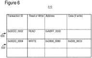
- Data set 502 is then stored in transaction table unit 510, which may be structured as illustrated in Figure 6 .
- the information illustrated in Figure 6 is related to two outstanding transactions, a read transaction 600 and a write transaction 602.
- Transaction table unit 510 is illustrated in Figure 6 as a table having a number of columns and rows. The number of rows corresponds to the number of outstanding transactions. In one embodiment, depending on the storage size of transaction table unit 510, completed transactions may be stored in addition to outstanding ones. In one embodiment, completed transactions are deleted one by one if more outstanding transactions are generated.
- the Figure 6 example shows a first column for a transaction identification number, a second column for the type of transaction, a third column for an address identifying the destination for the transaction, and a fourth column storing transaction-related information, for example, if the transaction is a write, its related data can be saved. More columns may be added as necessary. For example, depending on the computing device's protocol, it may be necessary to have a column indicating whether the transaction is outstanding or not.
- the transaction table unit stores transactions where a slave unit response is expected.
- the transaction table unit would typically store all transactions from its associated master unit. If more master units are associated with the transaction table unit, then an extra column may identify which transaction corresponds to which master unit.
- the transaction logger device can optionally filter out transactions that do not require a response and only store transactions requiring a response.
- the transaction logger unit may also store transactions that do not require a response as long as the memory in the transaction logger unit is not needed by transactions requiring a response.
- this transaction When the response for a transaction is received, this transaction is marked as completed in the transaction table unit, and the transaction may be removed from the transaction table unit. As soon as the master unit initiates a new transaction, a new entry is added to the transaction table unit.
- the Transaction ID in Figure 6 is unique and can be used to handle the completion order of the transactions.
- an additional sequence number or a timestamp can be saved in the transaction table to provide additional information and to handle the completion order of the transactions
- the completed transaction could be marked as such, but kept until it must be deleted to log new transactions. Then, in addition to the record of the outstanding transactions, a certain number M of completed transactions can be kept in the transaction table unit, for example, in a first-in, first-out (FIFO) system.
- FIFO first-in, first-out
- transaction logger device 210a may also include a shadow transaction table unit 514 configured to save information from transaction table unit 510.
- logic 512 coordinates with transaction table unit 510 and shadow transaction table unit 514 to copy information from one to the other.
- logic 512 receives a shutdown signal 506 from a shutdown port 526.
- the shutdown signal 506 may be generated, for example, by the computing device user pushing a restart button.
- This action triggers a reset control 540 to generate shutdown signal 506.
- a path 542 followed by this signal from reset control 540 to port 526 is independent of the master unit served by the transaction logger device 210a or other master units or slave units so that failure of these units does not affect this path.
- transaction logger device 210a becomes aware that the system is going to be restarted and saves information from transaction table unit 510 to shadow transaction table unit 514.
- shadow transaction table unit 514 may be a storage device.
- shutdown signal 506 is triggered by a watchdog timer 544 that monitors, for example, a master unit corresponding to transaction logger device 210a.
- Shutdown signal 506 may be generated, for example, when the watchdog timer times out, as will be explained later.
- a path 546 followed by this signal from watchdog timer 544 to reset control 540 is independent of the master unit served by transaction logger device 210a or other master or slave units so that failure of these units does not affect this path. In this way, just prior to restarting the computing system, transaction logger device 210a becomes aware that the system is going to be restarted and thus, it saves information from transaction table unit 510 to shadow transaction table unit 514.
- Transaction logger device 210a may also have a debug port 550 that communicates with a device external to the computing device for transferring the information stored in transaction table unit 510 or in shadow transaction table unit 514. This configuration is helpful if there is no shadow transaction table unit 514 and transaction table unit 510 does not preserve the information over the shutdown of the computing device. With this port in place, when the system hangs, it is possible to extract the information from the transaction table unit and store it in an outside storage device 560 prior to shutting down the computing device.
- Port 550 may be, for example, a debug port such as JTAG (Joint Test Action Group, which is the common name for the IEEE 1149.1 Standard Test Access Port and Boundary-Scan Architecture).
- Computing device 700 may include one or more of the features discussed above with regard to Figures 2-6 .
- computing device 700 is considered to have a transaction logger device for each master unit.
- Computing device 700 includes, in this embodiment, first master unit 702a (a processor), second master unit 702b (graphic processing unit), third master unit 702c (video accelerator), and fourth master unit 702d (modem hardware accelerator; note that the modem hardware accelerator is just an example and it should not be construed to limit the invention to those devices that include such accelerator. In other words, the novel concepts discussed herein apply to SoC or other computing devices that do not include a modem hardware accelerator).
- First master unit 702a may include some registers 702a-1, a floating point unit (FPU) 702a-2, an arithmetic logic unit 702a-3, an L1 data cache 702a-4, and an L1 instruction cache 702a-4.
- First master unit 702a has its own transaction logger device 710a. Note that comparing this embodiment to the structure illustrated in Figure 1 , transaction logger device 710a is in addition to cache unit 702a-4, which corresponds to cache 50 of the '946 patent. Transaction logger device 710a is shown in this embodiment to have splitter 710a-1, transaction table unit 710a-2 and shadow transaction table unit 710a-3, similar to the embodiment discussed in Figure 5 . Note that some transaction logger devices may have only transaction table unit 710a-2.
- Second master unit 702b may include a vertex processor 702b-1, a fragment processor 702b-2, a texture memory 702b-3, and other elements known by those skilled in the art. Second master unit 702b has its own transaction logger device 710b. Figure 7 also shows a slave unit 704-1, which happens to be a dynamic random access memory. Note that fourth master unit 702d may also act as a slave unit, as illustrated by path 712 from interconnect 706. Interconnect 706 may be connected to a boot read-only memory (ROM) 720 and to an on-chip static random access memory (SRAM) 722. A serial bus 726 is shown connecting the transaction logger devices to an external port 728. External port 728 is configured to be connected to an external storage device 730, for reasons to be discussed next.
- ROM boot read-only memory
- SRAM static random access memory
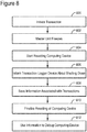
- step 800 A process of saving a record associated with uncompleted transactions is now discussed with regard to Figure 7 and the flowchart in Figure 8 .
- master unit 702a has initiated in step 800 some transactions with one or more slave units, and at least one transaction is outstanding.
- master unit 702a freezes. This error is overcome by initiating a reset action, in step 804, by computing device 700.
- the resetting may be triggered by a reset actor 746 (e.g., a tester pressing a reset button or an application processor) that has observed the computing device being unresponsive or by watchdog unit 740 as discussed above with regard to Figure 5 .
- a reset actor 746 e.g., a tester pressing a reset button or an application processor
- the reset control 744 If the reset actor 746 initiates the reset, the reset control 744 generates the shutdown signal and sends it to transaction logger device 710a, along a path 742 independent of master unit 702a, so that the freeze condition of master unit 702a does not affect the ability of the reset control to communicate with the transaction logger device 710a. Similarly, if watchdog unit 740 detects that master unit 702a has stopped working, and an internal clock is timing out, watchdog unit 740 informs reset control 744, which sends the shut-down signal along path 742 directly to transaction logger device 710a. Reset control 744 is configured to communicate with one or more master units and to shut down them or the entire computing device if necessary.
- transaction logger device 710a is informed in step 806 about this imminent act.
- information (record) related to outstanding transactions is saved in step 808 in a more permanent manner so it survives restarting of the computing device.
- the computing device shut-down is finalized in step 810.
- a tester or engineer uses the saved record to debug the computing device once it is restarted.
- Step 808 may be implemented in different ways. A few examples are now discussed. According to a first implementation, consider that transaction logger device 710a has both the transaction table unit 710a-2 and shadow transaction table unit 710a-3. Further, consider that transaction table unit 710a-2 is a temporary memory and only shadow transaction table unit 710a-3 is a more permanent memory. Furthermore, assume that each master unit has its own transaction logger device with the above-noted structure.
- master unit is a processor as in Figure 7 , it can print the retrieved information to a console, save it to a file, display it on a screen, or even it via a short message (SMS) if the freeze happens in the field.
- SMS short message
- transaction table unit 710a-2 can be used as soon as the reset is released, it can be preferable to extract the information from the shadow transaction table unit and copy it to another memory location, like the on-chip SRAM 722 as soon as possible after reset to make sure the shadow transaction table unit is not overwritten with new information from transaction table unit 710a-2 in the event of a new reset.
- the record from the transaction table unit can be extracted, before the reset, for example, by using debug port 728 and associated serial bus 726.
- transaction logger device 710a has no shadow transaction table unit 710a-3.
- transaction logger device 710a has only transaction table unit 710a-2 for storing a record associated with outstanding transactions initiated by master unit 702a.
- the transaction table unit is designed such that the stored information persists over a reset.
- the shutdown signal triggers the transaction logger device 710a to mark transaction table unit 710a-2 as read-only.
- Transaction table unit 710a-2 remains read-only until its information has been copied to another device, e.g., memory 722 (on-chip SRAM in this embodiment) after reset. After the information is copied to another memory, the transaction table unit is re-enabled for writing, so new transactions are logged in.
- An advantage of this embodiment is that it requires less memory in the transaction logger device because it only needs to contain one transaction table unit.
- transaction table information for this embodiment.
- information from the transaction table unit can be extracted before the reset is completed. This can be implemented, as previously discussed, using debug port 728.
- each transaction table unit there is a single transaction table unit for each transaction logger device, and each master unit has its own transaction logger device.
- information in the transaction table unit is lost after a reset. This means that the record in the transaction table unit needs to be extracted before or during the reset.
- debug port 728 is used to extract the record of outstanding transactions from the transaction logger device.
- the method includes a step 900 of collecting, at a transaction logger device, a record associated with an outstanding transaction initiated by a computing device master unit, a step 902 of receiving a reset signal at the transaction logger device indicating that the computing device is going to be reset, and a step 904 of saving the record to survive the reset.
- the outstanding transaction is sent to a slave unit over an interconnect structure.
- One or more of the above-discussed embodiments advantageously saves a record of outstanding bus transactions when the system hangs, which is beneficial when trying to debug difficult system lockups. If a certain number M of completed transactions are kept in the transaction table unit in addition to uncompleted transactions, it is also possible to enhance the tester's ability to perform the debugging operation and more quickly identify the error causing the computing device to hang. Faster troubleshooting gives the manufacturer an edge bringing reliable products to market faster.
- the disclosed embodiments provide a computing device and method for collecting and saving information associated with outstanding transactions initiated by a master unit so that the information may be used after the computing device is reset. It should be understood that this description is not intended to limit the invention. On the contrary, the exemplary embodiments are intended to cover alternatives, modifications and equivalents, which are included in the spirit and scope of the invention as defined by the appended claims. Further, in the detailed description of the exemplary embodiments, numerous specific details are set forth in order to provide a comprehensive understanding of the claimed invention. However, one skilled in the art would understand that various embodiments may be practiced without such specific details.
- the exemplary embodiments may be embodied in a wireless communication device, a telecommunication network, as a method or in a computer program product. Accordingly, the exemplary embodiments may take the form of an entirely hardware embodiment or an embodiment combining hardware and software aspects. Further, the exemplary embodiments may take the form of a computer program product stored on a computer-readable storage medium having computer-readable instructions embodied in the medium. Any suitable computer-readable medium may be utilized, including hard disks, CD-ROMs, digital versatile disc (DVD), optical storage devices, or magnetic storage devices such a floppy disk or magnetic tape. Other non-limiting examples of computer readable media include flash-type memories or other known memories.
Landscapes
- Engineering & Computer Science (AREA)
- Theoretical Computer Science (AREA)
- General Engineering & Computer Science (AREA)
- Physics & Mathematics (AREA)
- General Physics & Mathematics (AREA)
- Computer Hardware Design (AREA)
- Quality & Reliability (AREA)
- Debugging And Monitoring (AREA)
Description
- The present invention generally relates to systems, software and methods and, more particularly, to mechanisms and techniques for recording information related to outstanding transactions in a computing device and saving the information to survive a reset of the computing device.
- An explosion of computing devices, stationary and portable, is currently underway. These computing devices include, but are not limited to, smartphones, laptops, tablets, phablets, etc. Demand for these devices is made more acute by social media's rapid evolution, which encourages a need to communicate and be in contact with others. This creates continual competition among various manufacturers to generate better and faster computing devices.
- However, an issue common to all these computing devices during development (and later) is reliability, i.e., the robustness, stability and interaction of their hardware and software. Most computer users have experienced the "blue screen of death," i.e., the screen computers typically show after a system failure, for whatever reason. Launching a computing device with this type of issue on the market can be very damaging to its manufacturer.
- To prevent or minimize this issue, manufacturers expend great effort (in both time and money) to debug and resolve potential errors of new devices. The faster these errors can be found and corrected, the faster the devices can be launched, generating income and positive press.
- Fear is high of launching a new computing device that is error-prone, so some manufacturers limit the volumes of initial new device being launched. If a problem is found early by customers or by the manufacturer's engineers, negative public feedback is minimized. However, this approach limits a manufacturer's income potential. If an error is found, it becomes the manufacturer's priority to identify which hardware component or line(s) of code caused the problem so adjustments can be made and production corrected and ramped up. If the error detection process is lengthy, which might be the case with complex computing devices, that product's future may be compromised.
- Thus, there is interest in mechanisms that quickly identify which hardware and/or code produces errors. A common and difficult error to solve in new computing devices is a system hang (or freeze). A hang can have several causes. Two such examples are now discussed. One involves a programming error, i.e., the computing device's software includes, for example, an infinite loop. More specifically, the infinite loop may be stuck on a spinlock in a kernel driver. Another example involves the processor's access to a hardware block that is not clocked or is powered off. In this situation, the processor enters into a real lockup during which the processor freezes and does not answer any interrupts. In the first example, it is possible to take control of the processor, for example, via a high-priority interrupt that a watchdog can trigger before it performs an actual system reset. With this interrupt handler, the operator may be able to dump as much information on the state of the device as possible (e.g., the content of the processor registers and of different memories). An engineer can then use this information to determine the cause of the system hang. In the second situation, it is much more difficult to find a freeze's root cause. Depending on the platform and hardware used in devices, different causes may be responsible for freezes or system failures.
- One approach for identifying errors in a new computing device is now discussed with regard to
U.S. Patent No. 7,447,946 , (the '946 patent herein) As illustrated inFigure 1 , which corresponds toFigure 1 of the '946 patent, adata processing apparatus 10 is a System-on-Chip (SoC) device havingplural master devices 30 and 40 connected through abus 20 to aslave device 60.Master devices 30 and 40 connect through acache 50 tobus 20. Other system devices andperipherals 65 may be connected tobus 20, some of which are master devices and others are slave devices. -
Cache 50 is configured to store information related to activities of the master modules. Based on this information, an engineer may determine an error indata processing device 10. Thus, the '946 patent solution relies on utilizing an existing cache connected to plural master devices. Information is saved in this cache together with data the cache would normally store. However,other master devices 65 do not have a cache, for example, modem hardware accelerators, graphics accelerators, direct memory access (DMA) controllers, video accelerators, microcontrollers such, as for example, ARM's M0-M4 series, etc. This means that if one of thesemaster devices 65 initiates a transaction on a bus that hangs the system, the engineer will not be able to find in thecache 50 information regarding that master device's activity prior to freezing, making it impossible to determine why there was a system hang. - In addition, because the '946 patent focuses on reusing a part of an existing cache, it will typically mean that the data processing device will only trace transactions when it knows in advance it will debug a problem or investigate performance. While this can be useful, it is very limiting and requires advance preparation, which might be a luxury when debugging a device. This is especially true for a modem in which network signaling and current radio conditions can result in very different system behavior that can take a long time to reproduce during problem troubleshooting.
- Further, selecting an existing cache to trace transactions only during debug sessions is intrusive because part of the cache cannot be used to cache the "usual data" at the same time. Furthermore, the '946 patent does not address at all the problem of losing information stored in the cache when the data processing device is reset.
-
US 6584586 discloses an external monitoring of accesses for capturing and transferring internal system activity of a computer under test. -
US 2011/202801 discloses a trace wherein transactions are prioritized differently and wherein transactions can be filtered based on the priority assigned to transactions for processing purposes when the trace flow is too high. D2 also discloses an alternative wherein the system is slowed down such that trace data of high priority can be processed by the system. -
EP 0664511 discloses a software log for a non-volatile memory with triggers in hardware such as address decoding logic and WDOG. -
US 2012/265910 discloses failover input/output devices to manage failover events of input/output controller devices that operate in accordance with e.g. a computer expansion card standard. -
US 2013/304955 discloses a system and method for trace multicast across a bus structure. - Thus, there is a need to develop a mechanism and a method capable of recording and preserving information related to an error affecting a computing device if the computing device shuts down. Accordingly, it would be desirable to provide devices, systems and methods that avoid the afore-described problems and drawbacks.
- Innovative computing devices may include hardware, software and complex interactions between these two components. Inevitably, due to the sheer complexity of these computing devices, internal errors remain undetected until the devices are sold on the market. Severe undetected errors undermine product credibility and, ultimately, manufacturer credibility. All errors slow down new product deployment. Thus, there a need for architecture and methods to facilitate early error detection.
- The invention is defined by the features laid down in the
independent claims 1 and 12. Further enhancements are provided by the dependent claims. - According to one embodiment, there is a computing device that includes at least one master unit, at least one slave unit, an interconnect structure configured to route transactions from the at least one master unit to the at least one slave unit, and a transaction logger device configured to intercept and save a record of outstanding transactions sent by the at least one master unit to the interconnect structure. The transaction logger device is further configured to preserve the record of outstanding transactions when at least part of the computing device is restarted.
- According to another embodiment, there is a method for preserving information after a computing device is reset. The method includes a step of collecting at a transaction logger device a record associated with an outstanding transaction initiated by a master unit of the computing device, a step of receiving a reset signal at the transaction logger device indicating that the computing device is going to be reset, and a step of saving the record to survive the reset. The outstanding transaction is sent to a slave unit over an interconnect structure.
- Thus, it is an object to overcome some of the deficiencies discussed in the previous section and to provide an architecture and/or method and/or computing device that includes a mechanism for storing error-related information and preserving it in case the computing device shuts down or freezes. One or more of the independent claims advantageously provides such a mechanism.
- The accompanying drawings, which are incorporated in and constitute a part of the specification, illustrate one or more embodiments and, together with the description, explain these embodiments. In the drawings:
-
Figure 1 is a schematic diagram of a conventional computing device; -
Figure 2 is a schematic diagram of a computing device in which each master unit has a transaction logger device; -
Figure 3 is a schematic diagram of a computing device in which plural master units share a transaction logger device; -
Figure 4 is a schematic diagram of a computing device in which all master units share a single transaction logger device; -
Figure 5 is a schematic diagram of a transaction logger device; -
Figure 6 schematically illustrates information stored in the transaction logger device; -
Figure 7 is a schematic illustration of a computing device with plural transaction logger devices; and -
Figures 8 and9 are flowcharts of methods for collecting and storing information associated with outstanding transactions initiated by a master unit in a computing device. - The following description of the exemplary embodiments refers to the accompanying drawings. The same reference numbers in different drawings identify the same or similar elements. The following detailed description does not limit the invention. Instead, the scope of the invention is defined by the appended claims. The following embodiments are discussed, for simplicity, with regard to the terminology and structure of a system-on-chip (SoC). However, the novel embodiments are not limited to SoC devices, but may be applied to other types of computing devices.
- Reference throughout the specification to "one embodiment" or "an embodiment" means that a particular feature, structure or characteristic described in connection with an embodiment is included in at least one embodiment of the present invention. Thus, the appearance of the phrases "in one embodiment" or "in an embodiment" in various places throughout the specification is not necessarily all referring to the same embodiment. Further, the particular features, structures or characteristics may be combined in any suitable manner in one or more embodiments.
- According to an embodiment, there is a computing device that includes at least one master unit, at least one slave unit and an interconnect structure connecting the at least one master unit to the at least one slave unit. The interconnect structure is configured to route transactions from the at least one master unit to the at least one slave unit. A transaction logger device is configured to receive and save a record of outstanding transactions initiated by the at least one master unit. The transaction logger device is also configured to preserve the record of outstanding transactions when the at least one master unit or the entire computing device are restarted. A more detailed discussion of this computing device is now presented. The computing device may include a SoC device and the master and slave units, and the interconnect structure may be part of the SoC device.
- It is believed that clarification for some terms used herein is in order. A SoC device, as the name suggests, is an integrated circuit that integrates all components of a computing device, e.g., smartphone, laptop, computer, tablet, phablet, MP3 player, DVD player, TV set or other electronic system into a single chip. The SoC device may contain digital, analog, mixed-signal, and often radiofrequency functions, all on the single chip substrate. Dedicated terminology for SoC is master unit, slave unit, interconnect. The following embodiments use, for simplicity, a SoC device having master units, slave units and an interconnect. However, these terms should not be construed to limit the applicability of the novel concepts discussed herein. In other words, these terms are also applicable to a non-SoC device.
- For example, a traditional computer includes, among other things, a processor, a memory, a graphic processor, a modem, graphics accelerators, a DMA controller, video accelerators, microcontrollers, etc. Some of these elements are considered to be master units while others are considered slave units. In one application, a master unit is any unit that initiates a transaction. A slave unit is any unit that acts upon the transaction. The interconnect is any bus structure over which these transactions are routed. Many embedded products presently use one of the AMBA (Advanced Microcontroller Bus Architecture) buses such as the AXI (Advanced eXtensible Interface) bus. This and many other bus architectures use the concept of a master and a slave. Simply put, a master can initiate a transaction on the bus, while a slave cannot.
- A transaction encompasses one or more operations that carry some form of data (or payload), but also operations that have no payload. The term "transaction" is considered in the following to encompass any information that may be indicative of an action started by the master unit. An example of an action started by the master unit is a "write" command or a "read" command. Those skilled in the art would recognize that the term "action" includes other activities performed by the master unit.
- The SoC device is used in the following to explain the novel features not only because it is currently used in mobile phone and other computing systems, but also because this type of device has specific features that create a specific class of errors as now discussed. For those SoC devices and others that are used on portable systems, power consumption is a matter of concern due to limited available battery power. Thus, SoC devices have different kinds of power management strategies, for example, one in which the clock for different hardware blocks is disabled (often referred to as clock gating) when the hardware block is not used. The different hardware blocks can also be powered off (often referred to as power gating) to save power. Thus, to save power, clock gating and/or power gating are applied to certain parts of the computing device that are not expected to be used.
- However, if a master unit initiates a read or write transaction on the AXI bus for a slave unit that is not clocked or powered, the slave unit cannot complete the transaction. Thus, the master unit trying to access that slave unit or trying to access through the same path of the interconnect will freeze. When this happens, it is currently not possible to determine which transaction was not completed. A reset of the computing device can be triggered, either manually by pressing a button, or automatically by a watchdog timer, which times out. However, after the reset, the information that could be used to troubleshoot the problem is normally erased.
- Thus, according to an embodiment illustrated in
Figure 2 , acomputing device 200 includes at least onemaster unit 202a, at least one slave unit 204-1, and aninterconnect 206 connected to the at least onemaster unit 202a and to the at least one slave unit 204-1.Interconnect 206 is configured to route transactions frommaster unit 202a to slave unit 204-1 or to another slave unit 204-2. Atransaction logger device 210a is configured to intercept and save a record of the outstanding transactions initiated bymaster unit 202a, andtransaction logger device 210a is also configured to preserve the record of outstanding transactions whenmaster unit 202a or other units are restarted. -
Computing device 200 is illustrated with only twomaster units interconnect 206 may be configured to connect any master unit to any slave unit. The embodiment illustrated inFigure 2 has a transaction logger device for each master unit, irrespective of the nature of the master unit. - However, in another embodiment illustrated in
Figure 3 , acomputing device 300 has a group ofmaster units transaction logger device 310a-b, while anothermaster unit 302c has its owntransaction logger device 310c. Another embodiment illustrated inFigure 4 has acomputing device 400 in which allmaster units 402a to 402c share a sametransaction logger device 410a-c. In one application, for any of the embodiments illustrated inFigures 2-4 , the transaction logger device's presence is not known by the master units. In other words, the master unit does not control its associated transaction logger device. In one application, the master unit is not even aware of the transaction logger device's existence. Thus, the transaction logger device acts similar to a spy, i.e., intercepts all communication between master unit and interconnect and extracts predetermined information without making these parties aware of its actions. This feature ensures that in a master unit freeze, the transaction logger device is free and/or independent of manipulating the stored data to preserve it during and after the master unit restart. - By adding a dedicated transaction logger device, it is possible to save most, if not all, uncompleted (or outstanding) transactions that a master unit initiates on the interconnect. In one embodiment illustrated in
Figure 5 , a more detailed inside structure oftransaction logger device 210a is illustrated. Information associated with the master unit'soutstanding transaction 500 may be saved in atransaction table unit 510. In one application,transaction table unit 510 is a memory storage device. More specifically,outstanding transaction 500 enterstransaction logger device 210a at aport 520 and then travels to asplitter 522, where adata set 502 is generated andoriginal transaction 500 is allowed to further travel toport 524, which communicates with the interconnect. In one application,data set 502 is identical tooutstanding transaction 500. However, in another application,original transaction 500 is processed atsplitter 522 to extractdata set 502, i.e., generate a record related tooutstanding transaction 500. Ifdata set 502 is identical tooutstanding transaction 500,logic 512 may act on it for extracting information related to the outstanding transaction, and the extracted information is stored intransaction table unit 510. -
Data set 502 is then stored intransaction table unit 510, which may be structured as illustrated inFigure 6 . The information illustrated inFigure 6 is related to two outstanding transactions, aread transaction 600 and awrite transaction 602. -
Transaction table unit 510 is illustrated inFigure 6 as a table having a number of columns and rows. The number of rows corresponds to the number of outstanding transactions. In one embodiment, depending on the storage size oftransaction table unit 510, completed transactions may be stored in addition to outstanding ones. In one embodiment, completed transactions are deleted one by one if more outstanding transactions are generated. TheFigure 6 example shows a first column for a transaction identification number, a second column for the type of transaction, a third column for an address identifying the destination for the transaction, and a fourth column storing transaction-related information, for example, if the transaction is a write, its related data can be saved. More columns may be added as necessary. For example, depending on the computing device's protocol, it may be necessary to have a column indicating whether the transaction is outstanding or not. - In one embodiment, the transaction table unit stores transactions where a slave unit response is expected. In a bus protocol where all transactions require a response, the transaction table unit would typically store all transactions from its associated master unit. If more master units are associated with the transaction table unit, then an extra column may identify which transaction corresponds to which master unit.
- For a bus protocol handling transactions where a response is unnecessary, the transaction logger device can optionally filter out transactions that do not require a response and only store transactions requiring a response. For this latter type of bus protocol, the transaction logger unit may also store transactions that do not require a response as long as the memory in the transaction logger unit is not needed by transactions requiring a response.
- When the response for a transaction is received, this transaction is marked as completed in the transaction table unit, and the transaction may be removed from the transaction table unit. As soon as the master unit initiates a new transaction, a new entry is added to the transaction table unit. In this example it is assumed that the Transaction ID in
Figure 6 is unique and can be used to handle the completion order of the transactions. Depending on the exact characteristics of the bus protocol, an additional sequence number or a timestamp can be saved in the transaction table to provide additional information and to handle the completion order of the transactions - Instead of deleting a completed transaction, the completed transaction could be marked as such, but kept until it must be deleted to log new transactions. Then, in addition to the record of the outstanding transactions, a certain number M of completed transactions can be kept in the transaction table unit, for example, in a first-in, first-out (FIFO) system. Thus, when a transaction is completed, it is not directly removed from the transaction table, but only marked COMPLETED. Then, when M completed transactions are in the table and new entries need to be added, the oldest completed transaction is removed and replaced with a new transaction. In this way it is possible to see more transaction history for a certain master unit. If a system hangs due to an uncompleted transaction, it is now possible to see which M transactions completed successfully before the uncompleted transaction. The information in the transaction table unit survives in some form a reset of the system as explained later.
- Returning to
Figure 5 ,transaction logger device 210a may also include a shadowtransaction table unit 514 configured to save information fromtransaction table unit 510. In one embodiment,logic 512 coordinates withtransaction table unit 510 and shadowtransaction table unit 514 to copy information from one to the other. - There are various mechanisms that trigger
logic 512 to act in this way. In one application,logic 512 receives ashutdown signal 506 from ashutdown port 526. Theshutdown signal 506 may be generated, for example, by the computing device user pushing a restart button. This action triggers areset control 540 to generateshutdown signal 506. Apath 542 followed by this signal fromreset control 540 toport 526 is independent of the master unit served by thetransaction logger device 210a or other master units or slave units so that failure of these units does not affect this path. In this way, just prior to restarting the computing system,transaction logger device 210a becomes aware that the system is going to be restarted and saves information fromtransaction table unit 510 to shadowtransaction table unit 514. In one application, shadowtransaction table unit 514 may be a storage device. - In another application,
shutdown signal 506 is triggered by awatchdog timer 544 that monitors, for example, a master unit corresponding totransaction logger device 210a.Shutdown signal 506 may be generated, for example, when the watchdog timer times out, as will be explained later. Apath 546 followed by this signal fromwatchdog timer 544 to resetcontrol 540 is independent of the master unit served bytransaction logger device 210a or other master or slave units so that failure of these units does not affect this path. In this way, just prior to restarting the computing system,transaction logger device 210a becomes aware that the system is going to be restarted and thus, it saves information fromtransaction table unit 510 to shadowtransaction table unit 514. -
Transaction logger device 210a may also have adebug port 550 that communicates with a device external to the computing device for transferring the information stored intransaction table unit 510 or in shadowtransaction table unit 514. This configuration is helpful if there is no shadowtransaction table unit 514 andtransaction table unit 510 does not preserve the information over the shutdown of the computing device. With this port in place, when the system hangs, it is possible to extract the information from the transaction table unit and store it in anoutside storage device 560 prior to shutting down the computing device.Port 550 may be, for example, a debug port such as JTAG (Joint Test Action Group, which is the common name for the IEEE 1149.1 Standard Test Access Port and Boundary-Scan Architecture). - A process of collecting and saving information associated with master unit transactions is now discussed in the context of
computing device 700, illustrated inFigure 7 .Computing device 700 may include one or more of the features discussed above with regard toFigures 2-6 . For simplicity of explanation,computing device 700 is considered to have a transaction logger device for each master unit.Computing device 700 includes, in this embodiment,first master unit 702a (a processor),second master unit 702b (graphic processing unit),third master unit 702c (video accelerator), andfourth master unit 702d (modem hardware accelerator; note that the modem hardware accelerator is just an example and it should not be construed to limit the invention to those devices that include such accelerator. In other words, the novel concepts discussed herein apply to SoC or other computing devices that do not include a modem hardware accelerator).First master unit 702a may include someregisters 702a-1, a floating point unit (FPU) 702a-2, anarithmetic logic unit 702a-3, anL1 data cache 702a-4, and anL1 instruction cache 702a-4.First master unit 702a has its owntransaction logger device 710a. Note that comparing this embodiment to the structure illustrated inFigure 1 ,transaction logger device 710a is in addition tocache unit 702a-4, which corresponds tocache 50 of the '946 patent.Transaction logger device 710a is shown in this embodiment to havesplitter 710a-1,transaction table unit 710a-2 and shadowtransaction table unit 710a-3, similar to the embodiment discussed inFigure 5 . Note that some transaction logger devices may have onlytransaction table unit 710a-2. -
Second master unit 702b may include avertex processor 702b-1, afragment processor 702b-2, atexture memory 702b-3, and other elements known by those skilled in the art.Second master unit 702b has its owntransaction logger device 710b.Figure 7 also shows a slave unit 704-1, which happens to be a dynamic random access memory. Note thatfourth master unit 702d may also act as a slave unit, as illustrated bypath 712 frominterconnect 706.Interconnect 706 may be connected to a boot read-only memory (ROM) 720 and to an on-chip static random access memory (SRAM) 722. Aserial bus 726 is shown connecting the transaction logger devices to anexternal port 728.External port 728 is configured to be connected to anexternal storage device 730, for reasons to be discussed next. - A process of saving a record associated with uncompleted transactions is now discussed with regard to
Figure 7 and the flowchart inFigure 8 . Suppose thatmaster unit 702a has initiated instep 800 some transactions with one or more slave units, and at least one transaction is outstanding. Instep 802, for any reason,master unit 702a freezes. This error is overcome by initiating a reset action, instep 804, by computingdevice 700. The resetting may be triggered by a reset actor 746 (e.g., a tester pressing a reset button or an application processor) that has observed the computing device being unresponsive or bywatchdog unit 740 as discussed above with regard toFigure 5 . If thereset actor 746 initiates the reset, thereset control 744 generates the shutdown signal and sends it totransaction logger device 710a, along apath 742 independent ofmaster unit 702a, so that the freeze condition ofmaster unit 702a does not affect the ability of the reset control to communicate with thetransaction logger device 710a. Similarly, ifwatchdog unit 740 detects thatmaster unit 702a has stopped working, and an internal clock is timing out,watchdog unit 740 informsreset control 744, which sends the shut-down signal alongpath 742 directly totransaction logger device 710a.Reset control 744 is configured to communicate with one or more master units and to shut down them or the entire computing device if necessary. - Thus, irrespective of how the computing device is being shut down (by parts or in its entirety), prior to this action,
transaction logger device 710a is informed instep 806 about this imminent act. As a consequence ofstep 806, information (record) related to outstanding transactions is saved instep 808 in a more permanent manner so it survives restarting of the computing device. Once the record is saved, the computing device shut-down is finalized instep 810. Then, instep 812, a tester or engineer uses the saved record to debug the computing device once it is restarted. - Step 808 may be implemented in different ways. A few examples are now discussed. According to a first implementation, consider that
transaction logger device 710a has both thetransaction table unit 710a-2 and shadowtransaction table unit 710a-3. Further, consider thattransaction table unit 710a-2 is a temporary memory and only shadowtransaction table unit 710a-3 is a more permanent memory. Furthermore, assume that each master unit has its own transaction logger device with the above-noted structure. - When a reset is triggered, a corresponding signal is sent from
reset control 744 totransaction logger device 710a, which reacts by copying the record fromtransaction table unit 710a-2 to shadowtransaction table unit 710a-3, which retains the information after the reset is released. Entries in shadowtransaction table unit 710a-3 can be extracted after the reset, whiletransaction table unit 710a-2 is used to log new transactions directly after the reset. Entries in shadowtransaction table unit 710a-3 can be retrieved in various ways after the computing device has restarted. For example,master unit 702a can read information from the shadow transaction table unit because the computing device has now been reset. Then, if master unit is a processor as inFigure 7 , it can print the retrieved information to a console, save it to a file, display it on a screen, or even it via a short message (SMS) if the freeze happens in the field. Even iftransaction table unit 710a-2 can be used as soon as the reset is released, it can be preferable to extract the information from the shadow transaction table unit and copy it to another memory location, like the on-chip SRAM 722 as soon as possible after reset to make sure the shadow transaction table unit is not overwritten with new information fromtransaction table unit 710a-2 in the event of a new reset. - In a variation of this embodiment, the record from the transaction table unit can be extracted, before the reset, for example, by using
debug port 728 and associatedserial bus 726. - In a different embodiment, assume that
transaction logger device 710a has no shadowtransaction table unit 710a-3. According to this embodiment,transaction logger device 710a has onlytransaction table unit 710a-2 for storing a record associated with outstanding transactions initiated bymaster unit 702a. The transaction table unit is designed such that the stored information persists over a reset. When a reset is triggered, the shutdown signal triggers thetransaction logger device 710a to marktransaction table unit 710a-2 as read-only.Transaction table unit 710a-2 remains read-only until its information has been copied to another device, e.g., memory 722 (on-chip SRAM in this embodiment) after reset. After the information is copied to another memory, the transaction table unit is re-enabled for writing, so new transactions are logged in. This means there is a certain time interval after the reset when no transactions can be logged in. This configuration is acceptable if the period during which the transaction table unit is read-only is kept short. An advantage of this embodiment is that it requires less memory in the transaction logger device because it only needs to contain one transaction table unit. - Different methods can be used to extract transaction table information for this embodiment. According to one approach, information from the transaction table unit can be extracted before the reset is completed. This can be implemented, as previously discussed, using
debug port 728. - In still another embodiment, there is a single transaction table unit for each transaction logger device, and each master unit has its own transaction logger device. However, in this embodiment, different from the others, information in the transaction table unit is lost after a reset. This means that the record in the transaction table unit needs to be extracted before or during the reset. Thus, according to this embodiment,
debug port 728 is used to extract the record of outstanding transactions from the transaction logger device. - A method for saving information associated with a computing device reset is now discussed with regard to
Figure 9 . The method includes astep 900 of collecting, at a transaction logger device, a record associated with an outstanding transaction initiated by a computing device master unit, astep 902 of receiving a reset signal at the transaction logger device indicating that the computing device is going to be reset, and astep 904 of saving the record to survive the reset. The outstanding transaction is sent to a slave unit over an interconnect structure. - One or more of the above-discussed embodiments advantageously saves a record of outstanding bus transactions when the system hangs, which is beneficial when trying to debug difficult system lockups. If a certain number M of completed transactions are kept in the transaction table unit in addition to uncompleted transactions, it is also possible to enhance the tester's ability to perform the debugging operation and more quickly identify the error causing the computing device to hang. Faster troubleshooting gives the manufacturer an edge bringing reliable products to market faster.
- The disclosed embodiments provide a computing device and method for collecting and saving information associated with outstanding transactions initiated by a master unit so that the information may be used after the computing device is reset. It should be understood that this description is not intended to limit the invention. On the contrary, the exemplary embodiments are intended to cover alternatives, modifications and equivalents, which are included in the spirit and scope of the invention as defined by the appended claims. Further, in the detailed description of the exemplary embodiments, numerous specific details are set forth in order to provide a comprehensive understanding of the claimed invention. However, one skilled in the art would understand that various embodiments may be practiced without such specific details.
- As also will be appreciated by one skilled in the art, the exemplary embodiments may be embodied in a wireless communication device, a telecommunication network, as a method or in a computer program product. Accordingly, the exemplary embodiments may take the form of an entirely hardware embodiment or an embodiment combining hardware and software aspects. Further, the exemplary embodiments may take the form of a computer program product stored on a computer-readable storage medium having computer-readable instructions embodied in the medium. Any suitable computer-readable medium may be utilized, including hard disks, CD-ROMs, digital versatile disc (DVD), optical storage devices, or magnetic storage devices such a floppy disk or magnetic tape. Other non-limiting examples of computer readable media include flash-type memories or other known memories.
- Although the features and elements of the present exemplary embodiments are described in the embodiments in particular combinations, each feature or element can be used alone without the other features and elements of the embodiments or in various combinations with or without other features and elements disclosed herein. The methods or flow charts provided in the present application may be implemented in a computer program, software or firmware tangibly embodied in a computer-readable storage medium for execution by a specifically programmed computer or processor.
Claims (15)
- A computing device (200) comprising:at least one master unit (202a);at least one slave unit (204-1);an interconnect structure (206) configured to route transactions from the at least one master unit (202a) to the at least one slave unit (204-1); anda transaction logger device (210a) configured to intercept all communication between a master unit and the interconnect structure and receive transactions sent by the at least one master unit (202a) to the at least one slave unit (204-1) via the interconnect structure (206), extract a data set from each of the received transactions, save the extracted data set as a record of outstanding transactions,wherein the transaction logger device (210a) is further configured to receive a reset signal independent of the at least one master unit, when a reset is triggered and preserve the record of outstanding transactions when at least a part of the computing device (200) is restarted.
- The computing device of claim 1, wherein the at least one master unit (202a) is restarted because it freezes and the transaction logger device (210a) stores the record of outstanding transactions prior to freezing.
- The computing device of claim 2, wherein the transaction logger device (210a) also stores a record of completed transactions.
- The computing device of claim 1, wherein the transaction logger device (210a) is independent of the at least one master unit (202a) and the transaction logger device's (210a) presence is unknown to the at least one master unit (202a).
- The computing device of claim 1, further comprising:additional master units (202b); andadditional transaction logger devices (210b).
- The computing device of claim 5, wherein each additional transaction logger device (210b) is associated with a corresponding additional master unit (210b).
- The computing device of claim 5, wherein plural master units (302a,302b) are associated with a single transaction logger device (310a-b).
- The computing device of claim 1, wherein the transaction logger device (210a) comprises:
a transaction table unit (510) configured to store the record of outstanding transactions. - The computing device of claim 8, wherein the transaction logger device further comprises:a shadow transaction table unit (514) configured to mirror the record of outstanding transactions from the transaction table unit (510),wherein the shadow transaction table unit (514) is configured to preserve its record after the at least one master unit (202a) is restarted while the transaction table unit (510) is configured to lose its record after the at least one master unit (202a) is restarted.
- The computing device of claim 9, further comprising:a port (526) configured to receive a reset instruction (506) based on which the transaction logger device (210a) copies the record of outstanding transactions from the transaction table unit (510) to the shadow transaction table unit (514) just prior to the reset,wherein the port (526) receives the reset instruction (506) independent of the at least one master unit (202a).
- The computing device of claim 10, wherein the reset instruction (506) is generated by a reset control (540) as a consequence of a reset button being pressed or of a watchdog device (544) monitoring the at least one master unit timing out.
- A method for preserving information after a reset of a computing device (200), the method comprising:intercepting, by a transaction logger device (210a), all communication between master unit (202a) and an interconnect structure (206), and thereby receiving, a transaction from a master unit (202a) to a slave unit (204-1) sent via the interconnect structure (206) of the computing device (200);extracting, by the transaction logger device (210a), a data set from the received transaction and saving the extracted data set as a record associated with the received transaction;receiving a reset signal at the transaction logger device (210a), independent of the master unit (202a), indicating that the computing device is going to be reset; andsaving the record of outstanding transactions to survive the reset.
- The method of claim 12, wherein the saving of the extracted data as the record involves saving the record to a transaction table unit (510) inside the transaction logger device (210a) when the outstanding transaction is initiated, the method further comprising;
copying the record to a shadow transaction table unit (514) inside the transaction logger device (210a) when the reset signal (506) is received,
wherein the shadow transaction table unit (514) maintains the record over the reset while the transaction table unit (510) loses the record over the reset. - The method of claim 12, wherein the saving of extracted data as the record involves saving the record to a transaction table unit (510) inside the transaction logger device (210a) when the outstanding transaction is initiated, the method further comprising:
changing a status of the transaction table unit (510) to a read-only status when the reset signal (506) is received. - The method of claim 12, wherein the step of saving comprises:
copying the record from the transaction table unit (510) to an external memory (560) when receiving the reset signal (506) and prior to resetting the computing device (200).
Applications Claiming Priority (2)
| Application Number | Priority Date | Filing Date | Title |
|---|---|---|---|
| US14/136,700 US9971716B2 (en) | 2013-12-20 | 2013-12-20 | Method, system and architecture for bus transaction logger |
| PCT/EP2014/076774 WO2015091032A1 (en) | 2013-12-20 | 2014-12-05 | Method, system and architecture for bus transaction logger |
Publications (2)
| Publication Number | Publication Date |
|---|---|
| EP3084609A1 EP3084609A1 (en) | 2016-10-26 |
| EP3084609B1 true EP3084609B1 (en) | 2020-06-10 |
Family
ID=52021193
Family Applications (1)
| Application Number | Title | Priority Date | Filing Date |
|---|---|---|---|
| EP14809823.9A Active EP3084609B1 (en) | 2013-12-20 | 2014-12-05 | Method, system and architecture for bus transaction logger |
Country Status (3)
| Country | Link |
|---|---|
| US (1) | US9971716B2 (en) |
| EP (1) | EP3084609B1 (en) |
| WO (1) | WO2015091032A1 (en) |
Families Citing this family (2)
| Publication number | Priority date | Publication date | Assignee | Title |
|---|---|---|---|---|
| US10218641B2 (en) * | 2015-10-09 | 2019-02-26 | Arris Enterprises Llc | Handling dynamic cascade port/LAG changes in a non-blocking manner |
| US11281837B2 (en) * | 2017-12-18 | 2022-03-22 | Intel Corporation | Router-based transaction routing for toggle reduction |
Family Cites Families (11)
| Publication number | Priority date | Publication date | Assignee | Title |
|---|---|---|---|---|
| AUPM348794A0 (en) | 1994-01-20 | 1994-02-17 | Alcatel Australia Limited | Microprocessor fault log |
| FR2715754B1 (en) * | 1994-02-01 | 1996-03-29 | Gemplus Card Int | Method for protecting the contact pads of a memory card. |
| US5938775A (en) * | 1997-05-23 | 1999-08-17 | At & T Corp. | Distributed recovery with κ-optimistic logging |
| US6584586B1 (en) * | 2000-03-22 | 2003-06-24 | Advanced Micro Devices, Inc. | Apparatus and method for capturing and transferring internal system activity |
| US7447946B2 (en) | 2004-11-05 | 2008-11-04 | Arm Limited | Storage of trace data within a data processing apparatus |
| JP2007226385A (en) * | 2006-02-22 | 2007-09-06 | Fujitsu Ltd | Message queue control program and message queuing system |
| US8069366B1 (en) * | 2009-04-29 | 2011-11-29 | Netapp, Inc. | Global write-log device for managing write logs of nodes of a cluster storage system |
| GB2477936B (en) | 2010-02-17 | 2016-02-10 | Advanced Risc Mach Ltd | Trace data priority selection |
| US8788873B2 (en) | 2011-04-14 | 2014-07-22 | Cisco Technology, Inc. | Server input/output failover device serving highly available virtual devices |
| US8838861B2 (en) | 2012-05-09 | 2014-09-16 | Qualcomm Incorporated | Methods and apparatuses for trace multicast across a bus structure, and related systems |
| CN103810074B (en) * | 2012-11-14 | 2017-12-29 | 华为技术有限公司 | A kind of on-chip system chip and corresponding monitoring method |
-
2013
- 2013-12-20 US US14/136,700 patent/US9971716B2/en active Active
-
2014
- 2014-12-05 WO PCT/EP2014/076774 patent/WO2015091032A1/en not_active Ceased
- 2014-12-05 EP EP14809823.9A patent/EP3084609B1/en active Active
Non-Patent Citations (1)
| Title |
|---|
| None * |
Also Published As
| Publication number | Publication date |
|---|---|
| US20150178232A1 (en) | 2015-06-25 |
| US9971716B2 (en) | 2018-05-15 |
| EP3084609A1 (en) | 2016-10-26 |
| WO2015091032A1 (en) | 2015-06-25 |
Similar Documents
| Publication | Publication Date | Title |
|---|---|---|
| TWI632462B (en) | Switching device and method for detecting i2c bus | |
| US7600055B2 (en) | Apparatus, system, and method for firmware update of redundant controllers | |
| KR102408053B1 (en) | System on chip, mobile terminal, and method for operating the system on chip | |
| US7992036B2 (en) | Apparatus, system, and method for volume-level restoration of cluster server data | |
| US10514972B2 (en) | Embedding forensic and triage data in memory dumps | |
| KR102695389B1 (en) | Systems, methods, and apparatus for crash recovery in storage devices | |
| CN114461341B (en) | A method, device and medium for preventing brain split of cloud platform virtual machine | |
| CN101271415A (en) | Realization method of monitoring watchdog in embedded equipment | |
| WO2021098485A1 (en) | Method and system for power-on and power-off control of pcie device | |
| US20140122421A1 (en) | Information processing apparatus, information processing method and computer-readable storage medium | |
| US20090113194A1 (en) | Persisting value relevant to debugging of computer system during reset of computer system | |
| CN101901177A (en) | Multi-core microprocessor and debugging method thereof | |
| US10746792B1 (en) | Debug mechanisms for a processor circuit | |
| CN115292077B (en) | Kernel exception handling methods and systems | |
| WO2024222707A1 (en) | Fault processing method and apparatus, and storage medium and electronic device | |
| US10157005B2 (en) | Utilization of non-volatile random access memory for information storage in response to error conditions | |
| CN103246591B (en) | Method and device for signal processing | |
| CN101025700A (en) | Abnormal reset system protection method and reset protection system | |
| US9971716B2 (en) | Method, system and architecture for bus transaction logger | |
| US9250942B2 (en) | Hardware emulation using on-the-fly virtualization | |
| CN100388215C (en) | Debug Support Unit and Debug Method Using Multiple Asynchronous Clocks on Chip Hardware | |
| CN118467256B (en) | Method, device, medium and product for recovering business faults of clusters | |
| CN104657229A (en) | Multi-core processor rollback recovering system and method based on high-availability hardware checking point | |
| JP2001101032A (en) | OS monitoring method by controlling between different types of OS | |
| CN109144760B (en) | Method, device, system and medium for acquiring memory state |
Legal Events
| Date | Code | Title | Description |
|---|---|---|---|
| PUAI | Public reference made under article 153(3) epc to a published international application that has entered the european phase |
Free format text: ORIGINAL CODE: 0009012 |
|
| 17P | Request for examination filed |
Effective date: 20160609 |
|
| AK | Designated contracting states |
Kind code of ref document: A1 Designated state(s): AL AT BE BG CH CY CZ DE DK EE ES FI FR GB GR HR HU IE IS IT LI LT LU LV MC MK MT NL NO PL PT RO RS SE SI SK SM TR |
|
| AX | Request for extension of the european patent |
Extension state: BA ME |
|
| RIN1 | Information on inventor provided before grant (corrected) |
Inventor name: MANSSON, STAFFAN Inventor name: ANYURU, ANDREAS Inventor name: TALLBERG, PER-INGE Inventor name: MORLAND, ULF |
|
| RIN1 | Information on inventor provided before grant (corrected) |
Inventor name: MANSSON, STAFFAN Inventor name: TALLBERG, PER-INGE Inventor name: ANYURU, ANDREAS Inventor name: MORLAND, ULF |
|
| DAX | Request for extension of the european patent (deleted) | ||
| RIC1 | Information provided on ipc code assigned before grant |
Ipc: G06F 11/14 20060101ALN20191210BHEP Ipc: G06F 13/362 20060101ALI20191210BHEP Ipc: G06F 11/34 20060101AFI20191210BHEP |
|
| RIC1 | Information provided on ipc code assigned before grant |
Ipc: G06F 11/14 20060101ALN20191216BHEP Ipc: G06F 11/34 20060101AFI20191216BHEP Ipc: G06F 13/362 20060101ALI20191216BHEP |
|
| GRAP | Despatch of communication of intention to grant a patent |
Free format text: ORIGINAL CODE: EPIDOSNIGR1 |
|
| STAA | Information on the status of an ep patent application or granted ep patent |
Free format text: STATUS: GRANT OF PATENT IS INTENDED |
|
| RIC1 | Information provided on ipc code assigned before grant |
Ipc: G06F 13/362 20060101ALI20200131BHEP Ipc: G06F 11/34 20060101AFI20200131BHEP Ipc: G06F 11/14 20060101ALN20200131BHEP |
|
| INTG | Intention to grant announced |
Effective date: 20200218 |
|
| GRAS | Grant fee paid |
Free format text: ORIGINAL CODE: EPIDOSNIGR3 |
|
| GRAA | (expected) grant |
Free format text: ORIGINAL CODE: 0009210 |
|
| STAA | Information on the status of an ep patent application or granted ep patent |
Free format text: STATUS: THE PATENT HAS BEEN GRANTED |
|
| AK | Designated contracting states |
Kind code of ref document: B1 Designated state(s): AL AT BE BG CH CY CZ DE DK EE ES FI FR GB GR HR HU IE IS IT LI LT LU LV MC MK MT NL NO PL PT RO RS SE SI SK SM TR |
|
| REG | Reference to a national code |
Ref country code: GB Ref legal event code: FG4D |
|
| REG | Reference to a national code |
Ref country code: AT Ref legal event code: REF Ref document number: 1279734 Country of ref document: AT Kind code of ref document: T Effective date: 20200615 Ref country code: CH Ref legal event code: EP |
|
| REG | Reference to a national code |
Ref country code: DE Ref legal event code: R096 Ref document number: 602014066514 Country of ref document: DE |
|
| REG | Reference to a national code |
Ref country code: IE Ref legal event code: FG4D |
|
| REG | Reference to a national code |
Ref country code: LT Ref legal event code: MG4D |
|
| PG25 | Lapsed in a contracting state [announced via postgrant information from national office to epo] |
Ref country code: FI Free format text: LAPSE BECAUSE OF FAILURE TO SUBMIT A TRANSLATION OF THE DESCRIPTION OR TO PAY THE FEE WITHIN THE PRESCRIBED TIME-LIMIT Effective date: 20200610 Ref country code: LT Free format text: LAPSE BECAUSE OF FAILURE TO SUBMIT A TRANSLATION OF THE DESCRIPTION OR TO PAY THE FEE WITHIN THE PRESCRIBED TIME-LIMIT Effective date: 20200610 Ref country code: GR Free format text: LAPSE BECAUSE OF FAILURE TO SUBMIT A TRANSLATION OF THE DESCRIPTION OR TO PAY THE FEE WITHIN THE PRESCRIBED TIME-LIMIT Effective date: 20200911 Ref country code: NO Free format text: LAPSE BECAUSE OF FAILURE TO SUBMIT A TRANSLATION OF THE DESCRIPTION OR TO PAY THE FEE WITHIN THE PRESCRIBED TIME-LIMIT Effective date: 20200910 Ref country code: SE Free format text: LAPSE BECAUSE OF FAILURE TO SUBMIT A TRANSLATION OF THE DESCRIPTION OR TO PAY THE FEE WITHIN THE PRESCRIBED TIME-LIMIT Effective date: 20200610 |
|
| REG | Reference to a national code |
Ref country code: NL Ref legal event code: MP Effective date: 20200610 |
|
| PG25 | Lapsed in a contracting state [announced via postgrant information from national office to epo] |
Ref country code: RS Free format text: LAPSE BECAUSE OF FAILURE TO SUBMIT A TRANSLATION OF THE DESCRIPTION OR TO PAY THE FEE WITHIN THE PRESCRIBED TIME-LIMIT Effective date: 20200610 Ref country code: BG Free format text: LAPSE BECAUSE OF FAILURE TO SUBMIT A TRANSLATION OF THE DESCRIPTION OR TO PAY THE FEE WITHIN THE PRESCRIBED TIME-LIMIT Effective date: 20200910 Ref country code: HR Free format text: LAPSE BECAUSE OF FAILURE TO SUBMIT A TRANSLATION OF THE DESCRIPTION OR TO PAY THE FEE WITHIN THE PRESCRIBED TIME-LIMIT Effective date: 20200610 Ref country code: LV Free format text: LAPSE BECAUSE OF FAILURE TO SUBMIT A TRANSLATION OF THE DESCRIPTION OR TO PAY THE FEE WITHIN THE PRESCRIBED TIME-LIMIT Effective date: 20200610 |
|
| REG | Reference to a national code |
Ref country code: AT Ref legal event code: MK05 Ref document number: 1279734 Country of ref document: AT Kind code of ref document: T Effective date: 20200610 |
|
| PG25 | Lapsed in a contracting state [announced via postgrant information from national office to epo] |
Ref country code: AL Free format text: LAPSE BECAUSE OF FAILURE TO SUBMIT A TRANSLATION OF THE DESCRIPTION OR TO PAY THE FEE WITHIN THE PRESCRIBED TIME-LIMIT Effective date: 20200610 Ref country code: NL Free format text: LAPSE BECAUSE OF FAILURE TO SUBMIT A TRANSLATION OF THE DESCRIPTION OR TO PAY THE FEE WITHIN THE PRESCRIBED TIME-LIMIT Effective date: 20200610 |
|
| PG25 | Lapsed in a contracting state [announced via postgrant information from national office to epo] |
Ref country code: EE Free format text: LAPSE BECAUSE OF FAILURE TO SUBMIT A TRANSLATION OF THE DESCRIPTION OR TO PAY THE FEE WITHIN THE PRESCRIBED TIME-LIMIT Effective date: 20200610 Ref country code: IT Free format text: LAPSE BECAUSE OF FAILURE TO SUBMIT A TRANSLATION OF THE DESCRIPTION OR TO PAY THE FEE WITHIN THE PRESCRIBED TIME-LIMIT Effective date: 20200610 Ref country code: SM Free format text: LAPSE BECAUSE OF FAILURE TO SUBMIT A TRANSLATION OF THE DESCRIPTION OR TO PAY THE FEE WITHIN THE PRESCRIBED TIME-LIMIT Effective date: 20200610 Ref country code: AT Free format text: LAPSE BECAUSE OF FAILURE TO SUBMIT A TRANSLATION OF THE DESCRIPTION OR TO PAY THE FEE WITHIN THE PRESCRIBED TIME-LIMIT Effective date: 20200610 Ref country code: ES Free format text: LAPSE BECAUSE OF FAILURE TO SUBMIT A TRANSLATION OF THE DESCRIPTION OR TO PAY THE FEE WITHIN THE PRESCRIBED TIME-LIMIT Effective date: 20200610 Ref country code: PT Free format text: LAPSE BECAUSE OF FAILURE TO SUBMIT A TRANSLATION OF THE DESCRIPTION OR TO PAY THE FEE WITHIN THE PRESCRIBED TIME-LIMIT Effective date: 20201012 Ref country code: CZ Free format text: LAPSE BECAUSE OF FAILURE TO SUBMIT A TRANSLATION OF THE DESCRIPTION OR TO PAY THE FEE WITHIN THE PRESCRIBED TIME-LIMIT Effective date: 20200610 Ref country code: RO Free format text: LAPSE BECAUSE OF FAILURE TO SUBMIT A TRANSLATION OF THE DESCRIPTION OR TO PAY THE FEE WITHIN THE PRESCRIBED TIME-LIMIT Effective date: 20200610 |
|
| PG25 | Lapsed in a contracting state [announced via postgrant information from national office to epo] |
Ref country code: IS Free format text: LAPSE BECAUSE OF FAILURE TO SUBMIT A TRANSLATION OF THE DESCRIPTION OR TO PAY THE FEE WITHIN THE PRESCRIBED TIME-LIMIT Effective date: 20201010 Ref country code: PL Free format text: LAPSE BECAUSE OF FAILURE TO SUBMIT A TRANSLATION OF THE DESCRIPTION OR TO PAY THE FEE WITHIN THE PRESCRIBED TIME-LIMIT Effective date: 20200610 Ref country code: SK Free format text: LAPSE BECAUSE OF FAILURE TO SUBMIT A TRANSLATION OF THE DESCRIPTION OR TO PAY THE FEE WITHIN THE PRESCRIBED TIME-LIMIT Effective date: 20200610 |
|
| REG | Reference to a national code |
Ref country code: DE Ref legal event code: R097 Ref document number: 602014066514 Country of ref document: DE |
|
| PLBE | No opposition filed within time limit |
Free format text: ORIGINAL CODE: 0009261 |
|
| STAA | Information on the status of an ep patent application or granted ep patent |
Free format text: STATUS: NO OPPOSITION FILED WITHIN TIME LIMIT |
|
| PG25 | Lapsed in a contracting state [announced via postgrant information from national office to epo] |
Ref country code: DK Free format text: LAPSE BECAUSE OF FAILURE TO SUBMIT A TRANSLATION OF THE DESCRIPTION OR TO PAY THE FEE WITHIN THE PRESCRIBED TIME-LIMIT Effective date: 20200610 |
|
| 26N | No opposition filed |
Effective date: 20210311 |
|
| PG25 | Lapsed in a contracting state [announced via postgrant information from national office to epo] |
Ref country code: SI Free format text: LAPSE BECAUSE OF FAILURE TO SUBMIT A TRANSLATION OF THE DESCRIPTION OR TO PAY THE FEE WITHIN THE PRESCRIBED TIME-LIMIT Effective date: 20200610 |
|
| REG | Reference to a national code |
Ref country code: CH Ref legal event code: PL |
|
| PG25 | Lapsed in a contracting state [announced via postgrant information from national office to epo] |
Ref country code: MC Free format text: LAPSE BECAUSE OF FAILURE TO SUBMIT A TRANSLATION OF THE DESCRIPTION OR TO PAY THE FEE WITHIN THE PRESCRIBED TIME-LIMIT Effective date: 20200610 |
|
| REG | Reference to a national code |
Ref country code: BE Ref legal event code: MM Effective date: 20201231 |
|
| PG25 | Lapsed in a contracting state [announced via postgrant information from national office to epo] |
Ref country code: IE Free format text: LAPSE BECAUSE OF NON-PAYMENT OF DUE FEES Effective date: 20201205 Ref country code: LU Free format text: LAPSE BECAUSE OF NON-PAYMENT OF DUE FEES Effective date: 20201205 |
|
| PG25 | Lapsed in a contracting state [announced via postgrant information from national office to epo] |
Ref country code: LI Free format text: LAPSE BECAUSE OF NON-PAYMENT OF DUE FEES Effective date: 20201231 Ref country code: CH Free format text: LAPSE BECAUSE OF NON-PAYMENT OF DUE FEES Effective date: 20201231 |
|
| PG25 | Lapsed in a contracting state [announced via postgrant information from national office to epo] |
Ref country code: TR Free format text: LAPSE BECAUSE OF FAILURE TO SUBMIT A TRANSLATION OF THE DESCRIPTION OR TO PAY THE FEE WITHIN THE PRESCRIBED TIME-LIMIT Effective date: 20200610 Ref country code: MT Free format text: LAPSE BECAUSE OF FAILURE TO SUBMIT A TRANSLATION OF THE DESCRIPTION OR TO PAY THE FEE WITHIN THE PRESCRIBED TIME-LIMIT Effective date: 20200610 Ref country code: CY Free format text: LAPSE BECAUSE OF FAILURE TO SUBMIT A TRANSLATION OF THE DESCRIPTION OR TO PAY THE FEE WITHIN THE PRESCRIBED TIME-LIMIT Effective date: 20200610 |
|
| PG25 | Lapsed in a contracting state [announced via postgrant information from national office to epo] |
Ref country code: MK Free format text: LAPSE BECAUSE OF FAILURE TO SUBMIT A TRANSLATION OF THE DESCRIPTION OR TO PAY THE FEE WITHIN THE PRESCRIBED TIME-LIMIT Effective date: 20200610 |
|
| PG25 | Lapsed in a contracting state [announced via postgrant information from national office to epo] |
Ref country code: BE Free format text: LAPSE BECAUSE OF NON-PAYMENT OF DUE FEES Effective date: 20201231 |
|
| PGFP | Annual fee paid to national office [announced via postgrant information from national office to epo] |
Ref country code: GB Payment date: 20251229 Year of fee payment: 12 |
|
| PGFP | Annual fee paid to national office [announced via postgrant information from national office to epo] |
Ref country code: FR Payment date: 20251226 Year of fee payment: 12 |
|
| PGFP | Annual fee paid to national office [announced via postgrant information from national office to epo] |
Ref country code: DE Payment date: 20251229 Year of fee payment: 12 |