EP3082257B1 - Anti snapback filter - Google Patents
Anti snapback filter Download PDFInfo
- Publication number
- EP3082257B1 EP3082257B1 EP15305580.1A EP15305580A EP3082257B1 EP 3082257 B1 EP3082257 B1 EP 3082257B1 EP 15305580 A EP15305580 A EP 15305580A EP 3082257 B1 EP3082257 B1 EP 3082257B1
- Authority
- EP
- European Patent Office
- Prior art keywords
- signal
- amplification device
- filtering means
- power amplifier
- value
- Prior art date
- Legal status (The legal status is an assumption and is not a legal conclusion. Google has not performed a legal analysis and makes no representation as to the accuracy of the status listed.)
- Not-in-force
Links
Images


Classifications
-
- H—ELECTRICITY
- H03—ELECTRONIC CIRCUITRY
- H03F—AMPLIFIERS
- H03F3/00—Amplifiers with only discharge tubes or only semiconductor devices as amplifying elements
- H03F3/20—Power amplifiers, e.g. Class B amplifiers, Class C amplifiers
- H03F3/24—Power amplifiers, e.g. Class B amplifiers, Class C amplifiers of transmitter output stages
- H03F3/245—Power amplifiers, e.g. Class B amplifiers, Class C amplifiers of transmitter output stages with semiconductor devices only
-
- H—ELECTRICITY
- H03—ELECTRONIC CIRCUITRY
- H03F—AMPLIFIERS
- H03F1/00—Details of amplifiers with only discharge tubes, only semiconductor devices or only unspecified devices as amplifying elements
- H03F1/32—Modifications of amplifiers to reduce non-linear distortion
- H03F1/3241—Modifications of amplifiers to reduce non-linear distortion using predistortion circuits
- H03F1/3247—Modifications of amplifiers to reduce non-linear distortion using predistortion circuits using feedback acting on predistortion circuits
-
- H—ELECTRICITY
- H03—ELECTRONIC CIRCUITRY
- H03F—AMPLIFIERS
- H03F1/00—Details of amplifiers with only discharge tubes, only semiconductor devices or only unspecified devices as amplifying elements
- H03F1/32—Modifications of amplifiers to reduce non-linear distortion
- H03F1/3241—Modifications of amplifiers to reduce non-linear distortion using predistortion circuits
- H03F1/3258—Modifications of amplifiers to reduce non-linear distortion using predistortion circuits based on polynomial terms
-
- H—ELECTRICITY
- H03—ELECTRONIC CIRCUITRY
- H03F—AMPLIFIERS
- H03F1/00—Details of amplifiers with only discharge tubes, only semiconductor devices or only unspecified devices as amplifying elements
- H03F1/34—Negative-feedback-circuit arrangements with or without positive feedback
-
- H—ELECTRICITY
- H03—ELECTRONIC CIRCUITRY
- H03F—AMPLIFIERS
- H03F1/00—Details of amplifiers with only discharge tubes, only semiconductor devices or only unspecified devices as amplifying elements
- H03F1/52—Circuit arrangements for protecting such amplifiers
- H03F1/523—Circuit arrangements for protecting such amplifiers for amplifiers using field-effect devices
-
- H—ELECTRICITY
- H03—ELECTRONIC CIRCUITRY
- H03F—AMPLIFIERS
- H03F3/00—Amplifiers with only discharge tubes or only semiconductor devices as amplifying elements
- H03F3/189—High frequency amplifiers, e.g. radio frequency amplifiers
- H03F3/19—High frequency amplifiers, e.g. radio frequency amplifiers with semiconductor devices only
- H03F3/195—High frequency amplifiers, e.g. radio frequency amplifiers with semiconductor devices only in integrated circuits
-
- H—ELECTRICITY
- H03—ELECTRONIC CIRCUITRY
- H03F—AMPLIFIERS
- H03F3/00—Amplifiers with only discharge tubes or only semiconductor devices as amplifying elements
- H03F3/20—Power amplifiers, e.g. Class B amplifiers, Class C amplifiers
- H03F3/24—Power amplifiers, e.g. Class B amplifiers, Class C amplifiers of transmitter output stages
-
- H—ELECTRICITY
- H04—ELECTRIC COMMUNICATION TECHNIQUE
- H04B—TRANSMISSION
- H04B1/00—Details of transmission systems, not covered by a single one of groups H04B3/00 - H04B13/00; Details of transmission systems not characterised by the medium used for transmission
- H04B1/02—Transmitters
- H04B1/04—Circuits
- H04B1/0475—Circuits with means for limiting noise, interference or distortion
-
- H—ELECTRICITY
- H03—ELECTRONIC CIRCUITRY
- H03F—AMPLIFIERS
- H03F2200/00—Indexing scheme relating to amplifiers
- H03F2200/171—A filter circuit coupled to the output of an amplifier
-
- H—ELECTRICITY
- H04—ELECTRIC COMMUNICATION TECHNIQUE
- H04B—TRANSMISSION
- H04B1/00—Details of transmission systems, not covered by a single one of groups H04B3/00 - H04B13/00; Details of transmission systems not characterised by the medium used for transmission
- H04B1/02—Transmitters
- H04B1/04—Circuits
- H04B2001/0408—Circuits with power amplifiers
- H04B2001/0425—Circuits with power amplifiers with linearisation using predistortion
-
- H—ELECTRICITY
- H04—ELECTRIC COMMUNICATION TECHNIQUE
- H04B—TRANSMISSION
- H04B1/00—Details of transmission systems, not covered by a single one of groups H04B3/00 - H04B13/00; Details of transmission systems not characterised by the medium used for transmission
- H04B1/02—Transmitters
- H04B1/04—Circuits
- H04B2001/0408—Circuits with power amplifiers
- H04B2001/0433—Circuits with power amplifiers with linearisation using feedback
Definitions
- the present invention generally relates to the field of communication networks, in particular to amplification devices for radio communication networks. More particularly, but not exclusively, the present invention relates to amplification devices adapted for being used in a remote radio head, for radiofrequency transmission.
- a generic common failure mode with transistor technology in particular with LDMOS (Laterally Diffused Metal Oxide Semiconductor) technology, has appeared inside the actual power amplifiers, especially at the highest power levels and across transistors suppliers. Over the last years several amplifiers have experienced similar failures across various manufacturers, geographic areas, and communication standards. The common point of failure has been the high power transistors in the power amplifiers.
- the failure analyses conducted by the transistor manufacturers indicate that the predominant root cause of failure is the presence of harmful signals in the radiofrequency input to the power amplifier. All standard generations, 2G, 3G, 4G are impacted. However the smart mobile phone introduction has accelerated the number of failures. These harmful signals are peak signals whose rise time is less than or equal to 10 ns.
- Some of these harmful signals are notably under the form of spikes, and cause the occurrence of a destructive phenomenon in the transistors, known as a snapback phenomenon. Symptoms of such a phenomenon are loss of gain and presence of a shunt path in the gate-source circuit of the transistor. Spikes are the physical phenomena of a mathematical function called Dirac delta.
- the source of the damaging input can be any part of the radio or of digital system prior to the input of the high power stage of the amplifier including the base band, the transmission radio, all algorithms and digital to analogue conversion. There are many variables that interact with each other in this issue including device characteristics, power amplifier design, radio system design, and the operating environment.
- Digital-to-analogue conversion by any of a variety of methods may be the source of harmful signals.
- the harmful signals have been generated by the signal-processing software in the base station.
- Digital PreDistortion (DPD) algorithms have also been implicated as a cause of these inputs.
- DPD Digital PreDistortion
- One known cause of these failures is the introduction of fast-rising pulses from the radio or other sources into the input of the high power stage of the amplifier.
- This harmful pulsed signal type can be produced by base station software, including DPD algorithms, 3GPP Release 99, High Speed Downlink Packet Algorithms and LTE (Long Term Evolution).
- Some experimental tests have shown that a specific source of harmful signals in the transmitter chain was a digitally-controlled attenuator in generator. This attenuator in generator has been shown to enter a low attenuation state at power on, and to produce high power bursts during certain state transitions.
- one known solution consists in reducing the drain voltage of transistor by 1 or 2 Volts.
- one drawback of this solution is that all amplification devices and radiofrequency transmitters impacted and situated in the same geographic area have to be returned to manufactory to set the new voltage or to change the supply power.
- reducing the drain voltage decreases the power capabilities of the devices.
- the amplification devices performances will be reduced.
- a main damage caused by this reduction in performances lies in a degradation of the amplification linearity.
- the modified devices will have to be tested again and some transistors will have to be replaced up the remote radio head measures meet the linearity specifications.
- this solution is provisional because in winter, at low temperature, transistors are more fragile and can break.
- US20140146918 discloses an amplification device of the prior art.
- an object of this invention is to provide a perennial solution for reducing the impact of harmful signals on the power amplifier of an amplification device, so as to avoid failure of said power amplifier, while not decreasing the power capabilities of the amplification device and not disturbing the amplification linearity.
- the present invention provides an amplification device according to the appended claims.
- the amplification device may include additional characteristics considered separately or combined, and notably:
- the present invention provides a radiofrequency transmitter comprising an amplification device as set forth above.
- the radiofrequency transmitter may include the additional characteristic wherein the filtering means of the amplification device are adapted to have an enlarged bandwidth compared to an effective bandwidth of the radiofrequency transmitter, said enlarged bandwidth encompassing said effective bandwidth.
- FIG. 1 shows a radiofrequency transmitter 2.
- the radiofrequency transmitter 2 is for example part of a remote radio head used as a communication relay in a communication network, for example a mobile communication network.
- the radiofrequency transmitter 2 comprises an amplification device 4 intended to provide the power required for the transmission of radio waves within this communication network.
- the radiofrequency transmitter 2 is adapted to receive a digital input signal 3A, from a first wired or wireless communication link 6A.
- the radiofrequency transmitter 2 is further adapted to provide an amplified analog output signal 3B, on a second wired or wireless communication link 6B.
- the received input signal 5A is for example a W-CDMA (Wideband Code Division Multiple Access), a LTE (Long-Term Evolution), a 2G, 3G, 4G, or a radio relay signal.
- W-CDMA Wideband Code Division Multiple Access
- LTE Long-Term Evolution
- the amplification device 4 is adapted to receive an input signal 5A and to provide an output signal 5B.
- the radiofrequency transmitter 2 includes, upstream of the amplification device 4, a digital processing stage which is not shown on Figure 1 for clarity reasons.
- the radiofrequency transmitter 2 further includes, downstream of the amplification device 4, a radiofrequency duplexer and an antenna which are not shown on Figure 1 for clarity reasons.
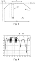
- the received input signal 5A has a frequency width Bsig, as shown in Figure 3 .
- the amplification device 4 comprises a predistortion loop 7.
- the predistortion loop 7 includes a predistortion module 8 adapted to provide a predistorded output signal 10 from the received input signal 5A, a power amplifier 14, and means 16 for filtering the predistorded output signal 10.
- the predistortion module 8 is a digital predistortion module which comprises a predistording functional block 20, a subtractor 22 and a digital predistorder 24.
- the predistortion module 8 is for example integrated within a FPGA (Field-Programmable Gate Array) or within an ASIC (Application-Specific Integrated Circuit).
- the predistording functional block 20 has a first input 26A and a second input 26B. It further has an output 28 connected to the input of the filtering means 16.
- the predistording functional block 20 is adapted to receive the input signal 5A on its first input 26A, and to provide the predistorded output signal 10 on its output 28.
- the predistorded output signal 10 is a digital signal.
- the non-inverting input of the subtractor 22 is connected to the output 28 of the predistording functional block 20.
- the output of the substractor 22 is adapted to provide a digital, time discrete error signal 29.
- the digital predistorder 24 has a first input 30A, a second input 30B, a first output 32A and a second output 32B.
- the first input 30A is connected to the output of the subtractor 22.
- the second input 30B is connected to the output of the power amplifier 14.
- the first output 32A is connected to the inverting input of the subtractor 22.
- the second output 32B is connected to the second input 26B of the predistording functional block 20.
- the digital predistorder 24 is adapted to receive, on its second input 30B, a feedback signal 34 from the output of the power amplifier 14.
- the feedback signal 34 is an analog and down-converted scaled version of the amplified output signal 5B.
- the feedback signal 34 is digitized by an analog-to-digital converter before being applied on the second input 30B, such a converter not being shown on Figure 2 for clarity reasons.
- the time discrete error signal 29 is calculated from the predistorded output signal 10 and the feedback signal 34.
- the predistortion module 8 is adapted to receive a feedback signal 34 from the output of the power amplifier 14, to determine a transmission characteristic of the power amplifier 14 from the received feedback signal 34, and to predistord the received input signal 5A according to the determined characteristic of the power amplifier 14.
- the predistortion module 8 is adapted to perform multiple iterations in order to determine the transmission characteristic of the power amplifier 14.
- the time discrete error signal 29 includes spectral portions related to the nonlinearities of the power amplifier 14. After some iterations within the predistortion loop 7, when the transmission characteristic of the power amplifier 14 have been determined, the value of the time discrete error signal 29 is almost zero and the predistording functional block 20 predistords the input signal 5A according to the determined characteristic of the power amplifier 14.
- the predistortion loop 7 forms a digital indirect learning predistortion loop. This allows to avoid distortion of the input signal 5A by the power amplifier 14, by determining the transmission characteristic of the power amplifier 14 during use of the amplification device 4, and by compensating upstream the effects of the nonlinearities of the power amplifier 14. Alternatively, the predistortion loop 7 forms a direct learning predistortion loop.
- the power amplifier 14 is adapted to provide the amplified output signal 5B.
- the power amplifier 14 comprises at least one semiconductor electronic component.
- the power amplifier 14 is an non-switched amplifier.
- the or each semiconductor electronic component is an analog radiofrequency component.
- the power amplifier 14 is a switched amplifier and the or each semiconductor electronic component is a switching electronic component.
- the or each semiconductor electronic component may be a transistor, for example a bipolar transistor or a field effect transistor.
- the or each semiconductor electronic component is an electronic field effect transistor, for example a LDMOS transistor.
- the or each electronic field effect transistor may be chosen from the non-limiting group consisting of: a VDMOS transistor, a CMOS transistor, a NMOS transistor, a PMOS transistor, a GaAs transistor and a GaN transistor.
- the power amplifier 14 further comprises at least one capacitor connected to a gate or a drain of the or one of the electronic field effect transistor(s). This feature allows to further enhance the protection of the field effect transistors by the filtering means 16, such a protection being detailed below.
- the filtering means 16 are connected between the predistortion module 8 and the power amplifier 14, and are adapted to provide a filtered signal 35 to the power amplifier 14.
- the filtering means 16 are analog filtering means and comprise an analog polynomial filter, for example a polynomial Chebyshev filter type.
- a digital-to-analog converter is arranged between the predistortion module 8 and the power amplifier 14. The digital-to-analog converter allows to convert the predistorded output signal 10 to an analog signal before it being processed by the filtering means 16.
- the filtering means 16 are digital filtering means.
- the filtering means 16 are for example integrated within the same FPGA or ASIC as that of the predistortion module 8, and a digital-to-analog converter is arranged between the filtering means 16 and the power amplifier 14.
- the filtering means 16 comprise a digital polynomial filter, for example a polynomial Chebyshev filter type.
- the filtering means 16 are configured to increase the rise time of any peak signal whose initial rise time is less than or equal to a predefined time value, and which is contained in the predistorded output signal 10, and to provide the resulting peak signal within the filtered signal 35 so as to protect the or each semiconductor electronic component.
- the or each resulting peak signal has a rise time greater than said predefined time value.
- the harmful peak signal is a spike
- the harmful peak signal has a rise time less than or equal to a predefined time value of 10 ns
- increasing the rise time of such a signal has the advantageous effect of cancelling the spike within the filtered signal 35.
- the filtering means 16 are advantageously configured to attenuate or cancel every peak signal having an initial rise time less than or equal to 10 ns, whatever its origin before the power amplifier 14 (modem, channel coding, base band, transmission part, predistortion module and so on). This allows to reduce the impact of such harmful peak signals on the power amplifier 14, while not decreasing the power capabilities of the amplification device 4 and not disturbing the amplification linearity, as will be detailed below.
- the filtering means 16 are adapted to have an enlarged bandwidth compared to an effective bandwidth ⁇ f of the radiofrequency transmitter 2.
- enlarged bandwidth it is meant in the following that the bandwidth of the filtering means 16 encompass the effective bandwidth ⁇ f of the radiofrequency transmitter 2.
- the filtering means 16 are adapted to have an upper cutoff frequency whose value is given by the sum between the value of the highest frequency of the frequency range ⁇ f of the received input signal 5A and the frequency width B sig of the input signal 5A times a numerical value.
- This numerical value is equal to 1 or 2. This allows to ensure that digital predistorder 24 gets a right image of distortion. More precisely, when the numerical value is equal to 1, as is the case in the embodiment of Figure 3 , such a design for the filtering means 16 allows not deforming the 3th order InterModulation (IMD3) component of the signal 10 predistorded by the predistortion module 8. When the numerical value is equal to 2, such a design for the filtering means 16 allows not deforming the IMD3 component and the 5th order InterModulation (IMD5) component of the predistorded signal 10.
- IMD3 3th order InterModulation
- IMD5 5th order InterModulation
- the filtering means 16 Since the filtering means 16 are included in the predistortion loop 7, the filtering means 16 must not attenuate the spectral portions related to the nonlinearities of the power amplifier 14 in the extreme cases where the received signal 5A is situated at the lowest or at the highest frequency of the effective bandwidth ⁇ f of the radiofrequency transmitter 2. In the exemplary embodiment of Figure 3 the received signal 5A is situated at the lowest frequency of the effective bandwidth ⁇ f of the radiofrequency transmitter 2.
- the filtering means 16 are adapted to have a predefined bandwidth B W19 , in particular a -19 dB bandwidth, which satisfies formula :
- B w 19 F 1 ⁇ ⁇ f + 2 ⁇ K 1 ⁇ B sig
- F 1 is a frequency value, in particular substantially equal to 200 MHz. The choice of this particular value for F1 allows to attenuate any peak signal contained in the predistorded output signal 10, whose rise time is less than or equal to 5 ns.
- K 1 is a numerical value between 1 and 3. When the numerical value K 1 is equal to 1, such a design for the filtering means 16 allows not deforming the IMD3 component of the signal 10 predistorded by the predistortion module 8. When the numerical value K 1 is equal to 3, such a design for the filtering means 16 allows not deforming the IMD3 component and the IMD5 component of the predistorded signal 10.
- the filtering means 16 are adapted to have a passband ripple whose value is more than or equal to -0.5 dB. This ensures that the amplitude variation versus frequency is in the range of digital equalization.
- the filtering means 16 are adapted to have insertion losses whose absolute value is more than or equal to -3 dB. This allows to ensure that the reserve gain for transmission is sufficient.
- the filtering means 16 are adapted to have a return loss whose absolute value is less than or equal to 10 dB. This allows to ensure that the filtering means 16 have a satisfactory adaptation to the impedance of the system.
- the filtering means 16 comprise an analog polynomial Chebyshev filter type. It is further assumed that the input signal 5A comprises several peak signals whose rise time is less than or equal to 10 ns, for example substantially equal to 5 ns. A point 36 represents each of these peak signals in the Bode diagram of Figure 3 .
- the predistording functional block 20 receives the input signal 5A on its first input 26A, and provides the predistorded output signal 10 on its output 28.
- the predistorded output signal 10 is a digital signal.
- the predistording functional block 20 predistords the input signal 5A according to the characteristic of the power amplifier 14, determined previously by the predistortion module 8 via the received feedback signal 34. Consequently, the predistorded output signal 10 comprises the spectral portions related to the nonlinearities of the power amplifier 14.
- the predistorded signal 10 is then transmitted to the filtering means 16. Thanks to their above-mentioned configuration, the filtering means 16 attenuate sufficiently each peak signal contained in the predistorded signal 10 to protect the or each semiconductor electronic component of the power amplifier 14. More precisely, the filtering means 16 increase the rise time of each peak signal contained in the predistorded signal 10, and provide within the filtered signal 35, for each initial peak signal, a resulting peak signal whose rise time is greater than 10 ns, so as to protect the or each semiconductor electronic component. This operation of the filtering means 16 is illustrated in Figures 4 to 6 .
- Figure 4 is a simulated timing diagram.
- the curve 38 represents the predistorded output signal 10 over time
- the curve 40 represents the filtered signal 35 over time. It can be seen from Figure 4 that every peak signal contained in the predistorded output signal 10 has been efficiently attenuated by the filtering means 16, since the curve 40 comprises no more peak signals whose rise time is less than or equal to 10 ns. Thus, the or each semiconductor electronic component of the power amplifier 14 is efficiently protected by the filtering means 16.
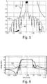
- Figure 5 is a simulated frequency diagram.
- the curve 42 represents the frequency spectrum of the predistorded output signal 10, and the curve 44 represents the frequency spectrum of the filtered signal 35.
- the curve 46 represents the transfer function of the filtering means 16. From Figure 5 it can be seen how the filtering means 16 modify the frequency spectrum of the predistorded output signal 10.
- the cardinal sine portions appearing on the curve 42 are due to a particular peak signal contained in the predistorded output signal 10, which is represented in Figure 6 .
- This particular peak signal is a square signal with a strong level.
- Figure 6 is a simulated timing diagram, in which the curve 48 represents this undesired square signal over time, and the curve 50 represents the square signal over time, when filtered by the filtering means 16. From Figure 6 it can be seen that the filtering means 16 smoothen the edges of the undesired square signal so that the rise time of this signal increases up to acceptable values, i.e. to values greater than 10 ns. Thus, the or each semiconductor electronic component of the power amplifier 14 is efficiently protected by the filtering means 16.
- test bench was configured to generate many peak signals having a rise time less than or equal to 10 ns.
- the predistortion module 8, the filtering means 16 and the power amplifier 14 have been connected downstream to the test bench.
- the tests have shown that with the filtering means 16 compliant to the above-mentioned configuration, peak signals having a rise time less than or equal to 10 ns have been detected upstream of the filtering means 16, but that no such peak signal has been detected downstream of the filtering means 16.
- the characteristic and performances of the semiconductor electronic components such as gain, efficiency, linearity have been checked with success, i.e. no degradation in these parameters was detected. Tests have been repeated with different types of semiconductor electronic components and none of them broke. The same semiconductor electronic components have been tested again without the filtering means 16 and have been destroyed due to the harmful peak signals.
- the filtering means 16 comprise a stripline filter 52.
- the stripline filter 52 is a coupled line filter which has two metallic electrodes 54, for example two copper electrodes 54.
- the use of such a stripline filter for the filtering means 16 allows reducing the design time of the filtering means.
- the filtering means 16 comprise a dielectric filter 56.
- the filtering means 16 comprise a cavity filter 58.
- a cavity filter can be easily inserted within a cabinet at the output of the predistortion module 8.
- Each of these three embodiments for the filtering means 16, illustrated on Figures 7 to 9 allows providing a low volume for the filtering means. This facilitates the insertion of the filtering means within the amplification device 4, in particular when the amplification device 4 is used as a radiofrequency amplification device.
- the amplification device allows reducing the impact of harmful signals on the power amplifier so as to avoid failure of said power amplifier, while not decreasing the power capabilities of the amplification device and not disturbing the amplification linearity.
- the amplification device according to the invention has the further advantage that the filtering means can be integrated within the device either at the initial design phase of the device, or directly onsite afterwards, without requiring any additional add-on or hardware.
- any block diagrams herein represent conceptual views of illustrative circuitry embodying the principles of the invention.
- any flow charts, flow diagrams, state transition diagrams, pseudo code, and the like represent various processes which may be substantially represented in computer readable medium and so executed by a computer or processor, whether or not such computer or processor is explicitly shown.
Description
- The present invention generally relates to the field of communication networks, in particular to amplification devices for radio communication networks. More particularly, but not exclusively, the present invention relates to amplification devices adapted for being used in a remote radio head, for radiofrequency transmission.
- A generic common failure mode with transistor technology, in particular with LDMOS (Laterally Diffused Metal Oxide Semiconductor) technology, has appeared inside the actual power amplifiers, especially at the highest power levels and across transistors suppliers. Over the last years several amplifiers have experienced similar failures across various manufacturers, geographic areas, and communication standards. The common point of failure has been the high power transistors in the power amplifiers. The failure analyses conducted by the transistor manufacturers indicate that the predominant root cause of failure is the presence of harmful signals in the radiofrequency input to the power amplifier. All standard generations, 2G, 3G, 4G are impacted. However the smart mobile phone introduction has accelerated the number of failures. These harmful signals are peak signals whose rise time is less than or equal to 10 ns. Some of these harmful signals are notably under the form of spikes, and cause the occurrence of a destructive phenomenon in the transistors, known as a snapback phenomenon. Symptoms of such a phenomenon are loss of gain and presence of a shunt path in the gate-source circuit of the transistor. Spikes are the physical phenomena of a mathematical function called Dirac delta.
- This harmful impact of such a snapback phenomenon in the transistors is known as a problem for a long time. It is likely that a switching mode will soon be introduced within the power amplifiers, for example for the new mobile format 5G, and hence that the power supplies will have a high speed of the voltage switching. It is largely predictable that some cautions will then have to be taken to avoid similar failures for LDMOS and the other transistor technologies like VDMOS (Vertically Diffused Metal Oxide Semiconductor), CMOS (Complementary metal oxide semi-conductor), NMOS (N-type metal-oxide-semiconductor), GaAs (Gallium Arsenide) and GaN (Gallium Nitride).
- The source of the damaging input can be any part of the radio or of digital system prior to the input of the high power stage of the amplifier including the base band, the transmission radio, all algorithms and digital to analogue conversion. There are many variables that interact with each other in this issue including device characteristics, power amplifier design, radio system design, and the operating environment.
- Digital-to-analogue conversion by any of a variety of methods may be the source of harmful signals. In some cases the harmful signals have been generated by the signal-processing software in the base station. Digital PreDistortion (DPD) algorithms have also been implicated as a cause of these inputs. One known cause of these failures is the introduction of fast-rising pulses from the radio or other sources into the input of the high power stage of the amplifier. This harmful pulsed signal type can be produced by base station software, including DPD algorithms, 3GPP Release 99, High Speed Downlink Packet Algorithms and LTE (Long Term Evolution). Some experimental tests have shown that a specific source of harmful signals in the transmitter chain was a digitally-controlled attenuator in generator. This attenuator in generator has been shown to enter a low attenuation state at power on, and to produce high power bursts during certain state transitions.
- Some solutions exist for reducing the impact of such harmful signals in the predistortion loop of an amplification device comprising a power amplifier, so as to avoid failure of the power amplifier.
- For example, one known solution consists in reducing the drain voltage of transistor by 1 or 2 Volts. However, one drawback of this solution is that all amplification devices and radiofrequency transmitters impacted and situated in the same geographic area have to be returned to manufactory to set the new voltage or to change the supply power. Besides, reducing the drain voltage decreases the power capabilities of the devices. As a consequence, the amplification devices performances will be reduced. A main damage caused by this reduction in performances lies in a degradation of the amplification linearity. As a result, the modified devices will have to be tested again and some transistors will have to be replaced up the remote radio head measures meet the linearity specifications. However, this solution is provisional because in winter, at low temperature, transistors are more fragile and can break.
US20140146918 discloses an amplification device of the prior art. - So an object of this invention is to provide a perennial solution for reducing the impact of harmful signals on the power amplifier of an amplification device, so as to avoid failure of said power amplifier, while not decreasing the power capabilities of the amplification device and not disturbing the amplification linearity.
- The present invention provides an amplification device according to the appended claims.
- The amplification device may include additional characteristics considered separately or combined, and notably:
- said at least one semiconductor electronic component is an analog radiofrequency semiconductor electronic component or a switching radiofrequency semiconductor electronic component;
- the filtering means are adapted to have an upper cutoff frequency whose value is given by a sum between a value of a highest frequency of a frequency range of the input signal and a value of a frequency width of the input signal times a numerical value, said numerical value being equal to 1 or 2 ;
- the filtering means are adapted to have a predefined bandwidth BW19, in particular a -19 dB bandwidth, which satisfies formula: B w19 = F 1 - Δ f + (2 - K1 )× Bsig, wherein F1 is a frequency value, in particular substantially equal to 200 MHz, Δf is the frequency range of the input signal, K1 is a numerical value between 1 and 3, and Bsig is the frequency width of the input signal ;
- the filtering means are adapted to have a passband ripple whose value is more than or equal to -0.5 dB ;
- the filtering means are adapted to have insertion losses whose value is more than or equal to -3 dB ;
- the filtering means are adapted to have a return loss whose value is less than or equal to 10 dB ;
- the at least one semiconductor electronic component is a bipolar transistor or an electronic field effect transistor;
- the power amplifier further comprises at least one capacitor, said at least one capacitor being connected to a gate or to a drain of the electronic field effect transistor;
- the filtering means comprise a digital or analog polynomial filter, for example a polynomial Chebyshev filter type ;
- the filtering means comprise a stripline filter or a dielectric filter or a cavity filter;
- the predistortion module is adapted to receive a feedback signal from an output of the power amplifier, to determine a transmission characteristic of the power amplifier from the received feedback signal, and to pre-distort the input signal according to said determined transmission characteristic of the power amplifier;
- said predefined time value is equal to 10 ns.
- According to a second aspect, the present invention provides a radiofrequency transmitter comprising an amplification device as set forth above.
- The radiofrequency transmitter may include the additional characteristic wherein the filtering means of the amplification device are adapted to have an enlarged bandwidth compared to an effective bandwidth of the radiofrequency transmitter, said enlarged bandwidth encompassing said effective bandwidth.
- Some embodiments of apparatus and/or methods in accordance with embodiments of the present invention are now described, by way of example only, and with reference to the accompanying drawings, in which :
- The
Figure 1 schematically and functionally illustrates a radiofrequency transmitter comprising an amplification device according to the present invention, - The
Figure 2 schematically and functionally illustrates the amplification device ofFigure 1 according to a first embodiment, said amplification device comprising a predistortion module providing a predistorded output signal, and means for filtering the predistorded output signal, - The
Figure 3 is a Bode diagram illustrating the transfer function of the filtering means ofFigure 2 , - The
Figure 4 is a simulated timing diagram illustrating a first unfiltered signal comprising peak signals, said first signal being provided by the predistortion module ofFigure 2 , and a second signal corresponding to the first signal which is filtered by a digital polynomial filter of the filtering means ofFigure 2 , - The
Figure 5 is a simulated frequency diagram illustrating a first unfiltered signal comprising peak signals, said first signal being provided by the predistortion module ofFigure 2 , and a second signal corresponding to the first signal which is filtered by an analog polynomial filter of the filtering means ofFigure 2 , - The
Figure 6 is a simulated timing diagram illustrating a first unfiltered signal causing the peak signals of the first unfiltered signal ofFigure 6 , and a second signal corresponding to the first signal which is filtered by an analog polynomial filter of the filtering means ofFigure 2 , - The
Figure 7 is a perspective view of the filtering means ofFigure 2 according to a particular embodiment, - The
Figures 8 and 9 are top views of the filtering means ofFigure 2 according to other alternative embodiments. -
Figure 1 shows a radiofrequency transmitter 2. The radiofrequency transmitter 2 is for example part of a remote radio head used as a communication relay in a communication network, for example a mobile communication network. The radiofrequency transmitter 2 comprises anamplification device 4 intended to provide the power required for the transmission of radio waves within this communication network. The radiofrequency transmitter 2 is adapted to receive adigital input signal 3A, from a first wired orwireless communication link 6A. The radiofrequency transmitter 2 is further adapted to provide an amplifiedanalog output signal 3B, on a second wired orwireless communication link 6B. The receivedinput signal 5A is for example a W-CDMA (Wideband Code Division Multiple Access), a LTE (Long-Term Evolution), a 2G, 3G, 4G, or a radio relay signal. - The
amplification device 4 is adapted to receive aninput signal 5A and to provide anoutput signal 5B. The radiofrequency transmitter 2 includes, upstream of theamplification device 4, a digital processing stage which is not shown onFigure 1 for clarity reasons. The radiofrequency transmitter 2 further includes, downstream of theamplification device 4, a radiofrequency duplexer and an antenna which are not shown onFigure 1 for clarity reasons. The receivedinput signal 5A has a frequency width Bsig, as shown inFigure 3 . - As shown in
Figure 2 , theamplification device 4 comprises apredistortion loop 7. Thepredistortion loop 7 includes apredistortion module 8 adapted to provide apredistorded output signal 10 from the receivedinput signal 5A, apower amplifier 14, and means 16 for filtering thepredistorded output signal 10. - In the exemplary embodiment of
Figure 2 , which is a synoptic and functional view, thepredistortion module 8 is a digital predistortion module which comprises a predistordingfunctional block 20, asubtractor 22 and adigital predistorder 24. Thepredistortion module 8 is for example integrated within a FPGA (Field-Programmable Gate Array) or within an ASIC (Application-Specific Integrated Circuit). - The predistording
functional block 20 has afirst input 26A and asecond input 26B. It further has anoutput 28 connected to the input of the filtering means 16. The predistordingfunctional block 20 is adapted to receive theinput signal 5A on itsfirst input 26A, and to provide thepredistorded output signal 10 on itsoutput 28. In this exemplary embodiment ofFigure 2 , thepredistorded output signal 10 is a digital signal. - The non-inverting input of the
subtractor 22 is connected to theoutput 28 of the predistordingfunctional block 20. The output of thesubstractor 22 is adapted to provide a digital, timediscrete error signal 29. - The
digital predistorder 24 has a first input 30A, asecond input 30B, afirst output 32A and asecond output 32B. The first input 30A is connected to the output of thesubtractor 22. Thesecond input 30B is connected to the output of thepower amplifier 14. Thefirst output 32A is connected to the inverting input of thesubtractor 22. Thesecond output 32B is connected to thesecond input 26B of the predistordingfunctional block 20. - The
digital predistorder 24 is adapted to receive, on itssecond input 30B, afeedback signal 34 from the output of thepower amplifier 14. - The
feedback signal 34 is an analog and down-converted scaled version of the amplifiedoutput signal 5B. Thefeedback signal 34 is digitized by an analog-to-digital converter before being applied on thesecond input 30B, such a converter not being shown onFigure 2 for clarity reasons. - The time
discrete error signal 29 is calculated from thepredistorded output signal 10 and thefeedback signal 34. - According to this exemplary embodiment of
Figure 2 , thepredistortion module 8 is adapted to receive afeedback signal 34 from the output of thepower amplifier 14, to determine a transmission characteristic of thepower amplifier 14 from the receivedfeedback signal 34, and to predistord the receivedinput signal 5A according to the determined characteristic of thepower amplifier 14. - More precisely, the
predistortion module 8 is adapted to perform multiple iterations in order to determine the transmission characteristic of thepower amplifier 14. When thepredistortion module 8 has not yet reached a state where the transmission characteristic of thepower amplifier 14 have been determined, the timediscrete error signal 29 includes spectral portions related to the nonlinearities of thepower amplifier 14. After some iterations within thepredistortion loop 7, when the transmission characteristic of thepower amplifier 14 have been determined, the value of the timediscrete error signal 29 is almost zero and the predistordingfunctional block 20 predistords theinput signal 5A according to the determined characteristic of thepower amplifier 14. - In this exemplary embodiment of
Figure 2 , thepredistortion loop 7 forms a digital indirect learning predistortion loop. This allows to avoid distortion of theinput signal 5A by thepower amplifier 14, by determining the transmission characteristic of thepower amplifier 14 during use of theamplification device 4, and by compensating upstream the effects of the nonlinearities of thepower amplifier 14. Alternatively, thepredistortion loop 7 forms a direct learning predistortion loop. - The
power amplifier 14 is adapted to provide the amplifiedoutput signal 5B. Thepower amplifier 14 comprises at least one semiconductor electronic component. - In the exemplary embodiment of
Figure 2 , thepower amplifier 14 is an non-switched amplifier. In this exemplary embodiment, the or each semiconductor electronic component is an analog radiofrequency component. In a variant not shown in the drawings, thepower amplifier 14 is a switched amplifier and the or each semiconductor electronic component is a switching electronic component. - The or each semiconductor electronic component may be a transistor, for example a bipolar transistor or a field effect transistor. In a particular exemplary embodiment, the or each semiconductor electronic component is an electronic field effect transistor, for example a LDMOS transistor. Alternatively, the or each electronic field effect transistor may be chosen from the non-limiting group consisting of: a VDMOS transistor, a CMOS transistor, a NMOS transistor, a PMOS transistor, a GaAs transistor and a GaN transistor. Preferably, according to this particular embodiment, the
power amplifier 14 further comprises at least one capacitor connected to a gate or a drain of the or one of the electronic field effect transistor(s). This feature allows to further enhance the protection of the field effect transistors by the filtering means 16, such a protection being detailed below. - The filtering means 16 are connected between the
predistortion module 8 and thepower amplifier 14, and are adapted to provide a filteredsignal 35 to thepower amplifier 14. - In the particular exemplary embodiment of
Figure 2 , the filtering means 16 are analog filtering means and comprise an analog polynomial filter, for example a polynomial Chebyshev filter type. In this exemplary embodiment ofFigure 2 , a digital-to-analog converter, not shown in the Figure for clarity reasons, is arranged between thepredistortion module 8 and thepower amplifier 14. The digital-to-analog converter allows to convert thepredistorded output signal 10 to an analog signal before it being processed by the filtering means 16. In a particular alternative not shown in the drawings, the filtering means 16 are digital filtering means. According to this alternative, the filtering means 16 are for example integrated within the same FPGA or ASIC as that of thepredistortion module 8, and a digital-to-analog converter is arranged between the filtering means 16 and thepower amplifier 14. According to an exemplary embodiment of this particular alternative, the filtering means 16 comprise a digital polynomial filter, for example a polynomial Chebyshev filter type. - The filtering means 16 are configured to increase the rise time of any peak signal whose initial rise time is less than or equal to a predefined time value, and which is contained in the
predistorded output signal 10, and to provide the resulting peak signal within the filteredsignal 35 so as to protect the or each semiconductor electronic component. The or each resulting peak signal has a rise time greater than said predefined time value. In the particular case wherein the harmful peak signal is a spike, i.e. the harmful peak signal has a rise time less than or equal to a predefined time value of 10 ns, increasing the rise time of such a signal has the advantageous effect of cancelling the spike within the filteredsignal 35. Thus, the filtering means 16 are advantageously configured to attenuate or cancel every peak signal having an initial rise time less than or equal to 10 ns, whatever its origin before the power amplifier 14 (modem, channel coding, base band, transmission part, predistortion module and so on). This allows to reduce the impact of such harmful peak signals on thepower amplifier 14, while not decreasing the power capabilities of theamplification device 4 and not disturbing the amplification linearity, as will be detailed below. - According to a preferred embodiment illustrated in
Figure 3 , the filtering means 16 are adapted to have an enlarged bandwidth compared to an effective bandwidth Δf of the radiofrequency transmitter 2. By "enlarged bandwidth" it is meant in the following that the bandwidth of the filtering means 16 encompass the effective bandwidth Δf of the radiofrequency transmitter 2. - Preferably, according to this preferred embodiment, the filtering means 16 are adapted to have an upper cutoff frequency whose value is given by the sum between the value of the highest frequency of the frequency range Δf of the received
input signal 5A and the frequency width Bsig of theinput signal 5A times a numerical value. This numerical value is equal to 1 or 2. This allows to ensure thatdigital predistorder 24 gets a right image of distortion. More precisely, when the numerical value is equal to 1, as is the case in the embodiment ofFigure 3 , such a design for the filtering means 16 allows not deforming the 3th order InterModulation (IMD3) component of thesignal 10 predistorded by thepredistortion module 8. When the numerical value is equal to 2, such a design for the filtering means 16 allows not deforming the IMD3 component and the 5th order InterModulation (IMD5) component of thepredistorded signal 10. - Since the filtering means 16 are included in the
predistortion loop 7, the filtering means 16 must not attenuate the spectral portions related to the nonlinearities of thepower amplifier 14 in the extreme cases where the receivedsignal 5A is situated at the lowest or at the highest frequency of the effective bandwidth Δf of the radiofrequency transmitter 2. In the exemplary embodiment ofFigure 3 the receivedsignal 5A is situated at the lowest frequency of the effective bandwidth Δf of the radiofrequency transmitter 2. In this exemplary embodiment, in order to satisfy the above-mentioned constraint, the filtering means 16 are adapted to have a predefined bandwidth BW19, in particular a -19 dB bandwidth, which satisfies formula :
- F1 is a frequency value, in particular substantially equal to 200 MHz. The choice of this particular value for F1 allows to attenuate any peak signal contained in the
predistorded output signal 10, whose rise time is less than or equal to 5 ns. K1 is a numerical value between 1 and 3. When the numerical value K1 is equal to 1, such a design for the filtering means 16 allows not deforming the IMD3 component of thesignal 10 predistorded by thepredistortion module 8. When the numerical value K1 is equal to 3, such a design for the filtering means 16 allows not deforming the IMD3 component and the IMD5 component of thepredistorded signal 10. - Preferably, the filtering means 16 are adapted to have a passband ripple whose value is more than or equal to -0.5 dB. This ensures that the amplitude variation versus frequency is in the range of digital equalization.
- Preferably again, the filtering means 16 are adapted to have insertion losses whose absolute value is more than or equal to -3 dB. This allows to ensure that the reserve gain for transmission is sufficient.
- Preferably again, the filtering means 16 are adapted to have a return loss whose absolute value is less than or equal to 10 dB. This allows to ensure that the filtering means 16 have a satisfactory adaptation to the impedance of the system.
- The operation of the
amplification device 4 will now be described with reference toFigures 2 to 6 . - It is assumed that the filtering means 16 comprise an analog polynomial Chebyshev filter type. It is further assumed that the
input signal 5A comprises several peak signals whose rise time is less than or equal to 10 ns, for example substantially equal to 5 ns. Apoint 36 represents each of these peak signals in the Bode diagram ofFigure 3 . - Firstly, the predistording
functional block 20 receives theinput signal 5A on itsfirst input 26A, and provides thepredistorded output signal 10 on itsoutput 28. In the exemplary embodiment ofFigure 2 , thepredistorded output signal 10 is a digital signal. - More precisely, the predistording
functional block 20 predistords theinput signal 5A according to the characteristic of thepower amplifier 14, determined previously by thepredistortion module 8 via the receivedfeedback signal 34. Consequently, thepredistorded output signal 10 comprises the spectral portions related to the nonlinearities of thepower amplifier 14. - The
predistorded signal 10 is then transmitted to the filtering means 16. Thanks to their above-mentioned configuration, the filtering means 16 attenuate sufficiently each peak signal contained in thepredistorded signal 10 to protect the or each semiconductor electronic component of thepower amplifier 14. More precisely, the filtering means 16 increase the rise time of each peak signal contained in thepredistorded signal 10, and provide within the filteredsignal 35, for each initial peak signal, a resulting peak signal whose rise time is greater than 10 ns, so as to protect the or each semiconductor electronic component. This operation of the filtering means 16 is illustrated inFigures 4 to 6 . -
Figure 4 is a simulated timing diagram. Thecurve 38 represents thepredistorded output signal 10 over time, and thecurve 40 represents the filteredsignal 35 over time. It can be seen fromFigure 4 that every peak signal contained in thepredistorded output signal 10 has been efficiently attenuated by the filtering means 16, since thecurve 40 comprises no more peak signals whose rise time is less than or equal to 10 ns. Thus, the or each semiconductor electronic component of thepower amplifier 14 is efficiently protected by the filtering means 16. -
Figure 5 is a simulated frequency diagram. Thecurve 42 represents the frequency spectrum of thepredistorded output signal 10, and thecurve 44 represents the frequency spectrum of the filteredsignal 35. Thecurve 46 represents the transfer function of the filtering means 16. FromFigure 5 it can be seen how the filtering means 16 modify the frequency spectrum of thepredistorded output signal 10. The cardinal sine portions appearing on thecurve 42 are due to a particular peak signal contained in thepredistorded output signal 10, which is represented inFigure 6 . This particular peak signal is a square signal with a strong level. -
Figure 6 is a simulated timing diagram, in which thecurve 48 represents this undesired square signal over time, and thecurve 50 represents the square signal over time, when filtered by the filtering means 16. FromFigure 6 it can be seen that the filtering means 16 smoothen the edges of the undesired square signal so that the rise time of this signal increases up to acceptable values, i.e. to values greater than 10 ns. Thus, the or each semiconductor electronic component of thepower amplifier 14 is efficiently protected by the filtering means 16. - Besides, some operational tests have been made in which a test bench was configured to generate many peak signals having a rise time less than or equal to 10 ns. The
predistortion module 8, the filtering means 16 and thepower amplifier 14 have been connected downstream to the test bench. The tests have shown that with the filtering means 16 compliant to the above-mentioned configuration, peak signals having a rise time less than or equal to 10 ns have been detected upstream of the filtering means 16, but that no such peak signal has been detected downstream of the filtering means 16. The characteristic and performances of the semiconductor electronic components such as gain, efficiency, linearity have been checked with success, i.e. no degradation in these parameters was detected. Tests have been repeated with different types of semiconductor electronic components and none of them broke. The same semiconductor electronic components have been tested again without the filtering means 16 and have been destroyed due to the harmful peak signals. - In the exemplary embodiment of
Figure 7 , the filtering means 16 comprise astripline filter 52. Thestripline filter 52 is a coupled line filter which has twometallic electrodes 54, for example twocopper electrodes 54. The use of such a stripline filter for the filtering means 16 allows reducing the design time of the filtering means. - In an alternative embodiment illustrated on
Figure 8 , the filtering means 16 comprise adielectric filter 56. - In another alternative embodiment illustrated on
Figure 9 , the filtering means 16 comprise acavity filter 58. Such a cavity filter can be easily inserted within a cabinet at the output of thepredistortion module 8. - Each of these three embodiments for the filtering means 16, illustrated on
Figures 7 to 9 , allows providing a low volume for the filtering means. This facilitates the insertion of the filtering means within theamplification device 4, in particular when theamplification device 4 is used as a radiofrequency amplification device. - Thus, the amplification device according to the invention allows reducing the impact of harmful signals on the power amplifier so as to avoid failure of said power amplifier, while not decreasing the power capabilities of the amplification device and not disturbing the amplification linearity.
- Moreover, the amplification device according to the invention has the further advantage that the filtering means can be integrated within the device either at the initial design phase of the device, or directly onsite afterwards, without requiring any additional add-on or hardware.
- It should be appreciated by those skilled in the art that any block diagrams herein represent conceptual views of illustrative circuitry embodying the principles of the invention. Similarly, it will be appreciated that any flow charts, flow diagrams, state transition diagrams, pseudo code, and the like represent various processes which may be substantially represented in computer readable medium and so executed by a computer or processor, whether or not such computer or processor is explicitly shown.
- The description and drawings merely illustrate the principles of the invention.
- Furthermore, all examples recited herein are principally intended expressly to be only for pedagogical purposes to aid the reader in understanding the principles of the invention and the concepts contributed by the inventor(s) to furthering the art, and are to be construed as being without limitation to such specifically recited examples and conditions. Moreover, all statements herein reciting principles, aspects, and embodiments of the invention, as well as specific examples thereof, are intended to encompass equivalents thereof.
Claims (14)
- Amplification device (4) adapted for being used in a radiofrequency transmitter (2), said amplification device (4) comprising a predistortion loop (7), said predistortion loop (7) including:• a predistortion module (8), adapted to provide a predistorded output signal (10) from a received input signal (5A),• a power amplifier (14), comprising at least one semiconductor electronic component, and• means (16) for filtering the predistorded output signal (10), said means (16) being connected between the predistortion module (8) and the power amplifier (14) and being adapted to provide a filtered signal (35) to the power amplifier (14),wherein the filtering means (16) are configured to increase the rise time of any peak signal whose initial rise time is less than or equal to a predefined time value, said peak signal being contained in the predistorded output signal (10), and to provide the resulting peak signal within the filtered signal (35) so as to protect the or each semiconductor electronic component, said resulting peak signal having a rise time greater than said predefined time value,
characterized in that the filtering means (16) are adapted to have an upper cutoff frequency whose value is given by a sum of a value of a highest frequency of an effective bandwidth (Δf) of the radiofrequency transmitter (2) and a value of a frequency width of the input signal (5A) times a numerical value, said numerical value being equal to 1 or 2. - Amplification device (4) according to claim 1, wherein said at least one semiconductor electronic component is an analog radiofrequency semiconductor electronic component or a switching radiofrequency semiconductor electronic component.
- Amplification device (4) according to any one of the preceding claims, wherein the filtering means (16) are adapted to have a predefined bandwidth BW19, in particular a -19 dB bandwidth, which satisfies formula: B w19 = F 1 - Δ f + (2 - K 1)× Bsig, wherein F1 is a frequency value, in particular substantially equal to 200 MHz, Δf is the effective bandwidth of the radiofrequency transmitter (2), K1 is a numerical value between 1 and 3, and Bsig is the frequency width of the input signal (5A).
- Amplification device (4) according to any one of the preceding claims, wherein the filtering means (16) are adapted to have a passband ripple whose value is more than or equal to -0.5 dB.
- Amplification device (4) according to any one of the preceding claims, wherein the filtering means (16) are adapted to have insertion losses whose value is more than or equal to -3 dB.
- Amplification device (4) according to any one of the preceding claims, wherein the filtering means (16) are adapted to have a return loss whose value is less than or equal to 10 dB.
- Amplification device (4) according to any one of the preceding claims, wherein the at least one semiconductor electronic component is a bipolar transistor or an electronic field effect transistor.
- Amplification device (4) according to claim 7, wherein the power amplifier (14) further comprises at least one capacitor, said at least one capacitor being connected to a gate or to a drain of the electronic field effect transistor.
- Amplification device (4) according to any one of the preceding claims, wherein the filtering means (16) comprise a digital or analog polynomial filter, for example a polynomial Chebyshev filter type.
- Amplification device (4) according to any one of the preceding claims, wherein the filtering means (16) comprise a stripline filter (52) or a dielectric filter (56) or a cavity filter (58).
- Amplification device (4) according to any one of the preceding claims, wherein the predistortion module (8) is adapted to receive a feedback signal (34) from an output of the power amplifier (14), to determine a transmission characteristic of the power amplifier (14) from the received feedback signal (34), and to pre-distort the input signal (5A) according to said determined transmission characteristic of the power amplifier (14).
- Amplification device (4) according to any one of the preceding claims, wherein said predefined time value is equal to 10 ns.
- Radiofrequency transmitter (2) comprising an amplification device (4) according to any of the preceding claims.
- Radiofrequency transmitter according to claim 13, wherein the filtering means (16) of the amplification device (4) are adapted to have an enlarged bandwidth compared to an effective bandwidth of the radiofrequency transmitter, said enlarged bandwidth encompassing said effective bandwidth.
Priority Applications (1)
| Application Number | Priority Date | Filing Date | Title |
|---|---|---|---|
| EP15305580.1A EP3082257B1 (en) | 2015-04-17 | 2015-04-17 | Anti snapback filter |
Applications Claiming Priority (1)
| Application Number | Priority Date | Filing Date | Title |
|---|---|---|---|
| EP15305580.1A EP3082257B1 (en) | 2015-04-17 | 2015-04-17 | Anti snapback filter |
Publications (2)
| Publication Number | Publication Date |
|---|---|
| EP3082257A1 EP3082257A1 (en) | 2016-10-19 |
| EP3082257B1 true EP3082257B1 (en) | 2018-06-27 |
Family
ID=53039830
Family Applications (1)
| Application Number | Title | Priority Date | Filing Date |
|---|---|---|---|
| EP15305580.1A Not-in-force EP3082257B1 (en) | 2015-04-17 | 2015-04-17 | Anti snapback filter |
Country Status (1)
| Country | Link |
|---|---|
| EP (1) | EP3082257B1 (en) |
Family Cites Families (2)
| Publication number | Priority date | Publication date | Assignee | Title |
|---|---|---|---|---|
| US20140146918A1 (en) * | 2012-11-27 | 2014-05-29 | Broadcom Corporation | Detection and Mitigation of an Abnormal Signal Condition Within a Power Amplifier (PA) |
| US20140294119A1 (en) * | 2013-06-13 | 2014-10-02 | Comtech Ef Data Corp. | System and Method for Distortion-Power Adapted Adaptive Pre-Distortion |
-
2015
- 2015-04-17 EP EP15305580.1A patent/EP3082257B1/en not_active Not-in-force
Non-Patent Citations (1)
| Title |
|---|
| None * |
Also Published As
| Publication number | Publication date |
|---|---|
| EP3082257A1 (en) | 2016-10-19 |
Similar Documents
| Publication | Publication Date | Title |
|---|---|---|
| US9787459B2 (en) | Non-linear interference cancellation for wireless transceivers | |
| Yu et al. | Band-limited Volterra series-based digital predistortion for wideband RF power amplifiers | |
| KR101845154B1 (en) | Device and method for adaptive crest-factor reduction in dynamic predistortion | |
| EP2438678B1 (en) | Apparatus and method for predictive over-drive detection | |
| KR102555331B1 (en) | Predistortion method for power amplifier and circuit therefor | |
| JP4868433B2 (en) | Distortion compensation apparatus and power amplification apparatus with distortion compensation function | |
| US8736379B1 (en) | Input match network for a power circuit | |
| US8970308B2 (en) | Input match network with RF bypass path | |
| KR20120116104A (en) | Power amplifier with advanced linearity | |
| US9214968B2 (en) | Apparatus and methods for providing a power amplifier with interference cancellation | |
| JP2006157917A (en) | Power amplifier | |
| Rudolph | GaN HEMTs for low-noise amplification—status and challenges | |
| KR100819307B1 (en) | Apparatus and method for input matching in power amplifier using delta-sigma modulated signal | |
| CN111147412B (en) | Predistortion processing device, signal transmission system and predistortion processing method | |
| EP3082257B1 (en) | Anti snapback filter | |
| Kumar et al. | Bandlimited DPD adapted APD for 5G communication | |
| EP3255791B1 (en) | Power amplifying equipment | |
| Manyam et al. | An FIR memory polynomial predistorter for wideband RF power amplifiers | |
| KR101093644B1 (en) | Analog feedback linear power amplifier using negative group delay circuits | |
| US20140010330A1 (en) | Transmission device and transmission method | |
| JP2014096794A (en) | Rf channel amplifier module having instantaneous power limiting function | |
| Le et al. | High efficiency 10 W GaN-HEMT power amplifier with optimum input stabilization | |
| US8427234B1 (en) | Method and apparatus for predistorting a signal | |
| Hamoud et al. | Evaluation of an optimal digital predistorter for multistandard systems | |
| KR100964335B1 (en) | Method for linearizing digital predistortion of power amplifier |
Legal Events
| Date | Code | Title | Description |
|---|---|---|---|
| PUAI | Public reference made under article 153(3) epc to a published international application that has entered the european phase |
Free format text: ORIGINAL CODE: 0009012 |
|
| AK | Designated contracting states |
Kind code of ref document: A1 Designated state(s): AL AT BE BG CH CY CZ DE DK EE ES FI FR GB GR HR HU IE IS IT LI LT LU LV MC MK MT NL NO PL PT RO RS SE SI SK SM TR |
|
| AX | Request for extension of the european patent |
Extension state: BA ME |
|
| STAA | Information on the status of an ep patent application or granted ep patent |
Free format text: STATUS: REQUEST FOR EXAMINATION WAS MADE |
|
| 17P | Request for examination filed |
Effective date: 20161128 |
|
| RBV | Designated contracting states (corrected) |
Designated state(s): AL AT BE BG CH CY CZ DE DK EE ES FI FR GB GR HR HU IE IS IT LI LT LU LV MC MK MT NL NO PL PT RO RS SE SI SK SM TR |
|
| STAA | Information on the status of an ep patent application or granted ep patent |
Free format text: STATUS: EXAMINATION IS IN PROGRESS |
|
| 17Q | First examination report despatched |
Effective date: 20170118 |
|
| RAP1 | Party data changed (applicant data changed or rights of an application transferred) |
Owner name: ALCATEL LUCENT |
|
| GRAP | Despatch of communication of intention to grant a patent |
Free format text: ORIGINAL CODE: EPIDOSNIGR1 |
|
| STAA | Information on the status of an ep patent application or granted ep patent |
Free format text: STATUS: GRANT OF PATENT IS INTENDED |
|
| GRAS | Grant fee paid |
Free format text: ORIGINAL CODE: EPIDOSNIGR3 |
|
| INTG | Intention to grant announced |
Effective date: 20180423 |
|
| GRAA | (expected) grant |
Free format text: ORIGINAL CODE: 0009210 |
|
| STAA | Information on the status of an ep patent application or granted ep patent |
Free format text: STATUS: THE PATENT HAS BEEN GRANTED |
|
| AK | Designated contracting states |
Kind code of ref document: B1 Designated state(s): AL AT BE BG CH CY CZ DE DK EE ES FI FR GB GR HR HU IE IS IT LI LT LU LV MC MK MT NL NO PL PT RO RS SE SI SK SM TR |
|
| REG | Reference to a national code |
Ref country code: GB Ref legal event code: FG4D |
|
| REG | Reference to a national code |
Ref country code: AT Ref legal event code: REF Ref document number: 1013203 Country of ref document: AT Kind code of ref document: T Effective date: 20180715 |
|
| REG | Reference to a national code |
Ref country code: IE Ref legal event code: FG4D |
|
| REG | Reference to a national code |
Ref country code: DE Ref legal event code: R096 Ref document number: 602015012697 Country of ref document: DE |
|
| PG25 | Lapsed in a contracting state [announced via postgrant information from national office to epo] |
Ref country code: SE Free format text: LAPSE BECAUSE OF FAILURE TO SUBMIT A TRANSLATION OF THE DESCRIPTION OR TO PAY THE FEE WITHIN THE PRESCRIBED TIME-LIMIT Effective date: 20180627 Ref country code: NO Free format text: LAPSE BECAUSE OF FAILURE TO SUBMIT A TRANSLATION OF THE DESCRIPTION OR TO PAY THE FEE WITHIN THE PRESCRIBED TIME-LIMIT Effective date: 20180927 Ref country code: LT Free format text: LAPSE BECAUSE OF FAILURE TO SUBMIT A TRANSLATION OF THE DESCRIPTION OR TO PAY THE FEE WITHIN THE PRESCRIBED TIME-LIMIT Effective date: 20180627 Ref country code: FI Free format text: LAPSE BECAUSE OF FAILURE TO SUBMIT A TRANSLATION OF THE DESCRIPTION OR TO PAY THE FEE WITHIN THE PRESCRIBED TIME-LIMIT Effective date: 20180627 Ref country code: BG Free format text: LAPSE BECAUSE OF FAILURE TO SUBMIT A TRANSLATION OF THE DESCRIPTION OR TO PAY THE FEE WITHIN THE PRESCRIBED TIME-LIMIT Effective date: 20180927 |
|
| REG | Reference to a national code |
Ref country code: NL Ref legal event code: MP Effective date: 20180627 |
|
| REG | Reference to a national code |
Ref country code: LT Ref legal event code: MG4D |
|
| PG25 | Lapsed in a contracting state [announced via postgrant information from national office to epo] |
Ref country code: GR Free format text: LAPSE BECAUSE OF FAILURE TO SUBMIT A TRANSLATION OF THE DESCRIPTION OR TO PAY THE FEE WITHIN THE PRESCRIBED TIME-LIMIT Effective date: 20180928 Ref country code: RS Free format text: LAPSE BECAUSE OF FAILURE TO SUBMIT A TRANSLATION OF THE DESCRIPTION OR TO PAY THE FEE WITHIN THE PRESCRIBED TIME-LIMIT Effective date: 20180627 Ref country code: HR Free format text: LAPSE BECAUSE OF FAILURE TO SUBMIT A TRANSLATION OF THE DESCRIPTION OR TO PAY THE FEE WITHIN THE PRESCRIBED TIME-LIMIT Effective date: 20180627 Ref country code: LV Free format text: LAPSE BECAUSE OF FAILURE TO SUBMIT A TRANSLATION OF THE DESCRIPTION OR TO PAY THE FEE WITHIN THE PRESCRIBED TIME-LIMIT Effective date: 20180627 |
|
| REG | Reference to a national code |
Ref country code: AT Ref legal event code: MK05 Ref document number: 1013203 Country of ref document: AT Kind code of ref document: T Effective date: 20180627 |
|
| PG25 | Lapsed in a contracting state [announced via postgrant information from national office to epo] |
Ref country code: NL Free format text: LAPSE BECAUSE OF FAILURE TO SUBMIT A TRANSLATION OF THE DESCRIPTION OR TO PAY THE FEE WITHIN THE PRESCRIBED TIME-LIMIT Effective date: 20180627 |
|
| PG25 | Lapsed in a contracting state [announced via postgrant information from national office to epo] |
Ref country code: SK Free format text: LAPSE BECAUSE OF FAILURE TO SUBMIT A TRANSLATION OF THE DESCRIPTION OR TO PAY THE FEE WITHIN THE PRESCRIBED TIME-LIMIT Effective date: 20180627 Ref country code: CZ Free format text: LAPSE BECAUSE OF FAILURE TO SUBMIT A TRANSLATION OF THE DESCRIPTION OR TO PAY THE FEE WITHIN THE PRESCRIBED TIME-LIMIT Effective date: 20180627 Ref country code: RO Free format text: LAPSE BECAUSE OF FAILURE TO SUBMIT A TRANSLATION OF THE DESCRIPTION OR TO PAY THE FEE WITHIN THE PRESCRIBED TIME-LIMIT Effective date: 20180627 Ref country code: EE Free format text: LAPSE BECAUSE OF FAILURE TO SUBMIT A TRANSLATION OF THE DESCRIPTION OR TO PAY THE FEE WITHIN THE PRESCRIBED TIME-LIMIT Effective date: 20180627 Ref country code: IS Free format text: LAPSE BECAUSE OF FAILURE TO SUBMIT A TRANSLATION OF THE DESCRIPTION OR TO PAY THE FEE WITHIN THE PRESCRIBED TIME-LIMIT Effective date: 20181027 Ref country code: AT Free format text: LAPSE BECAUSE OF FAILURE TO SUBMIT A TRANSLATION OF THE DESCRIPTION OR TO PAY THE FEE WITHIN THE PRESCRIBED TIME-LIMIT Effective date: 20180627 Ref country code: PL Free format text: LAPSE BECAUSE OF FAILURE TO SUBMIT A TRANSLATION OF THE DESCRIPTION OR TO PAY THE FEE WITHIN THE PRESCRIBED TIME-LIMIT Effective date: 20180627 |
|
| PG25 | Lapsed in a contracting state [announced via postgrant information from national office to epo] |
Ref country code: IT Free format text: LAPSE BECAUSE OF FAILURE TO SUBMIT A TRANSLATION OF THE DESCRIPTION OR TO PAY THE FEE WITHIN THE PRESCRIBED TIME-LIMIT Effective date: 20180627 Ref country code: SM Free format text: LAPSE BECAUSE OF FAILURE TO SUBMIT A TRANSLATION OF THE DESCRIPTION OR TO PAY THE FEE WITHIN THE PRESCRIBED TIME-LIMIT Effective date: 20180627 Ref country code: ES Free format text: LAPSE BECAUSE OF FAILURE TO SUBMIT A TRANSLATION OF THE DESCRIPTION OR TO PAY THE FEE WITHIN THE PRESCRIBED TIME-LIMIT Effective date: 20180627 |
|
| REG | Reference to a national code |
Ref country code: DE Ref legal event code: R097 Ref document number: 602015012697 Country of ref document: DE |
|
| PLBE | No opposition filed within time limit |
Free format text: ORIGINAL CODE: 0009261 |
|
| STAA | Information on the status of an ep patent application or granted ep patent |
Free format text: STATUS: NO OPPOSITION FILED WITHIN TIME LIMIT |
|
| PG25 | Lapsed in a contracting state [announced via postgrant information from national office to epo] |
Ref country code: DK Free format text: LAPSE BECAUSE OF FAILURE TO SUBMIT A TRANSLATION OF THE DESCRIPTION OR TO PAY THE FEE WITHIN THE PRESCRIBED TIME-LIMIT Effective date: 20180627 |
|
| 26N | No opposition filed |
Effective date: 20190328 |
|
| PG25 | Lapsed in a contracting state [announced via postgrant information from national office to epo] |
Ref country code: SI Free format text: LAPSE BECAUSE OF FAILURE TO SUBMIT A TRANSLATION OF THE DESCRIPTION OR TO PAY THE FEE WITHIN THE PRESCRIBED TIME-LIMIT Effective date: 20180627 |
|
| REG | Reference to a national code |
Ref country code: DE Ref legal event code: R119 Ref document number: 602015012697 Country of ref document: DE |
|
| PG25 | Lapsed in a contracting state [announced via postgrant information from national office to epo] |
Ref country code: AL Free format text: LAPSE BECAUSE OF FAILURE TO SUBMIT A TRANSLATION OF THE DESCRIPTION OR TO PAY THE FEE WITHIN THE PRESCRIBED TIME-LIMIT Effective date: 20180627 |
|
| REG | Reference to a national code |
Ref country code: CH Ref legal event code: PL |
|
| REG | Reference to a national code |
Ref country code: BE Ref legal event code: MM Effective date: 20190430 |
|
| GBPC | Gb: european patent ceased through non-payment of renewal fee |
Effective date: 20190417 |
|
| PG25 | Lapsed in a contracting state [announced via postgrant information from national office to epo] |
Ref country code: LU Free format text: LAPSE BECAUSE OF NON-PAYMENT OF DUE FEES Effective date: 20190417 Ref country code: MC Free format text: LAPSE BECAUSE OF FAILURE TO SUBMIT A TRANSLATION OF THE DESCRIPTION OR TO PAY THE FEE WITHIN THE PRESCRIBED TIME-LIMIT Effective date: 20180627 |
|
| PG25 | Lapsed in a contracting state [announced via postgrant information from national office to epo] |
Ref country code: DE Free format text: LAPSE BECAUSE OF NON-PAYMENT OF DUE FEES Effective date: 20191101 Ref country code: LI Free format text: LAPSE BECAUSE OF NON-PAYMENT OF DUE FEES Effective date: 20190430 Ref country code: CH Free format text: LAPSE BECAUSE OF NON-PAYMENT OF DUE FEES Effective date: 20190430 Ref country code: GB Free format text: LAPSE BECAUSE OF NON-PAYMENT OF DUE FEES Effective date: 20190417 |
|
| PG25 | Lapsed in a contracting state [announced via postgrant information from national office to epo] |
Ref country code: BE Free format text: LAPSE BECAUSE OF NON-PAYMENT OF DUE FEES Effective date: 20190430 Ref country code: FR Free format text: LAPSE BECAUSE OF NON-PAYMENT OF DUE FEES Effective date: 20190430 |
|
| PG25 | Lapsed in a contracting state [announced via postgrant information from national office to epo] |
Ref country code: TR Free format text: LAPSE BECAUSE OF FAILURE TO SUBMIT A TRANSLATION OF THE DESCRIPTION OR TO PAY THE FEE WITHIN THE PRESCRIBED TIME-LIMIT Effective date: 20180627 |
|
| PG25 | Lapsed in a contracting state [announced via postgrant information from national office to epo] |
Ref country code: IE Free format text: LAPSE BECAUSE OF NON-PAYMENT OF DUE FEES Effective date: 20190417 |
|
| PG25 | Lapsed in a contracting state [announced via postgrant information from national office to epo] |
Ref country code: PT Free format text: LAPSE BECAUSE OF FAILURE TO SUBMIT A TRANSLATION OF THE DESCRIPTION OR TO PAY THE FEE WITHIN THE PRESCRIBED TIME-LIMIT Effective date: 20181029 |
|
| PG25 | Lapsed in a contracting state [announced via postgrant information from national office to epo] |
Ref country code: CY Free format text: LAPSE BECAUSE OF FAILURE TO SUBMIT A TRANSLATION OF THE DESCRIPTION OR TO PAY THE FEE WITHIN THE PRESCRIBED TIME-LIMIT Effective date: 20180627 |
|
| PG25 | Lapsed in a contracting state [announced via postgrant information from national office to epo] |
Ref country code: HU Free format text: LAPSE BECAUSE OF FAILURE TO SUBMIT A TRANSLATION OF THE DESCRIPTION OR TO PAY THE FEE WITHIN THE PRESCRIBED TIME-LIMIT; INVALID AB INITIO Effective date: 20150417 Ref country code: MT Free format text: LAPSE BECAUSE OF FAILURE TO SUBMIT A TRANSLATION OF THE DESCRIPTION OR TO PAY THE FEE WITHIN THE PRESCRIBED TIME-LIMIT Effective date: 20180627 |
|
| PG25 | Lapsed in a contracting state [announced via postgrant information from national office to epo] |
Ref country code: MK Free format text: LAPSE BECAUSE OF FAILURE TO SUBMIT A TRANSLATION OF THE DESCRIPTION OR TO PAY THE FEE WITHIN THE PRESCRIBED TIME-LIMIT Effective date: 20180627 |