EP3082171A1 - Composition for anode buffer layer of organic thin film solar cell and organic thin film solar cell - Google Patents
Composition for anode buffer layer of organic thin film solar cell and organic thin film solar cell Download PDFInfo
- Publication number
- EP3082171A1 EP3082171A1 EP14870013.1A EP14870013A EP3082171A1 EP 3082171 A1 EP3082171 A1 EP 3082171A1 EP 14870013 A EP14870013 A EP 14870013A EP 3082171 A1 EP3082171 A1 EP 3082171A1
- Authority
- EP
- European Patent Office
- Prior art keywords
- group
- thin film
- composition
- buffer layer
- solar cell
- Prior art date
- Legal status (The legal status is an assumption and is not a legal conclusion. Google has not performed a legal analysis and makes no representation as to the accuracy of the status listed.)
- Granted
Links
- 0 *c1cc(Oc(c(F)c(c(-c(c(F)c(c(Oc2cc(S(O)(=O)=O)cc3c2ccc(S(O)(=O)=O)c3)c2F)F)c2F)c2F)F)c2F)c(ccc(S(O)(=O)=O)c2)c2c1 Chemical compound *c1cc(Oc(c(F)c(c(-c(c(F)c(c(Oc2cc(S(O)(=O)=O)cc3c2ccc(S(O)(=O)=O)c3)c2F)F)c2F)c2F)F)c2F)c(ccc(S(O)(=O)=O)c2)c2c1 0.000 description 1
Classifications
-
- H—ELECTRICITY
- H10—SEMICONDUCTOR DEVICES; ELECTRIC SOLID-STATE DEVICES NOT OTHERWISE PROVIDED FOR
- H10K—ORGANIC ELECTRIC SOLID-STATE DEVICES
- H10K85/00—Organic materials used in the body or electrodes of devices covered by this subclass
- H10K85/60—Organic compounds having low molecular weight
- H10K85/631—Amine compounds having at least two aryl rest on at least one amine-nitrogen atom, e.g. triphenylamine
-
- C—CHEMISTRY; METALLURGY
- C07—ORGANIC CHEMISTRY
- C07C—ACYCLIC OR CARBOCYCLIC COMPOUNDS
- C07C309/00—Sulfonic acids; Halides, esters, or anhydrides thereof
- C07C309/01—Sulfonic acids
- C07C309/28—Sulfonic acids having sulfo groups bound to carbon atoms of six-membered aromatic rings of a carbon skeleton
- C07C309/41—Sulfonic acids having sulfo groups bound to carbon atoms of six-membered aromatic rings of a carbon skeleton containing singly-bound oxygen atoms bound to the carbon skeleton
- C07C309/43—Sulfonic acids having sulfo groups bound to carbon atoms of six-membered aromatic rings of a carbon skeleton containing singly-bound oxygen atoms bound to the carbon skeleton having at least one of the sulfo groups bound to a carbon atom of a six-membered aromatic ring being part of a condensed ring system
-
- C—CHEMISTRY; METALLURGY
- C07—ORGANIC CHEMISTRY
- C07C—ACYCLIC OR CARBOCYCLIC COMPOUNDS
- C07C211/00—Compounds containing amino groups bound to a carbon skeleton
- C07C211/43—Compounds containing amino groups bound to a carbon skeleton having amino groups bound to carbon atoms of six-membered aromatic rings of the carbon skeleton
- C07C211/54—Compounds containing amino groups bound to a carbon skeleton having amino groups bound to carbon atoms of six-membered aromatic rings of the carbon skeleton having amino groups bound to two or three six-membered aromatic rings
-
- C—CHEMISTRY; METALLURGY
- C07—ORGANIC CHEMISTRY
- C07C—ACYCLIC OR CARBOCYCLIC COMPOUNDS
- C07C211/00—Compounds containing amino groups bound to a carbon skeleton
- C07C211/43—Compounds containing amino groups bound to a carbon skeleton having amino groups bound to carbon atoms of six-membered aromatic rings of the carbon skeleton
- C07C211/54—Compounds containing amino groups bound to a carbon skeleton having amino groups bound to carbon atoms of six-membered aromatic rings of the carbon skeleton having amino groups bound to two or three six-membered aromatic rings
- C07C211/55—Diphenylamines
-
- C—CHEMISTRY; METALLURGY
- C08—ORGANIC MACROMOLECULAR COMPOUNDS; THEIR PREPARATION OR CHEMICAL WORKING-UP; COMPOSITIONS BASED THEREON
- C08G—MACROMOLECULAR COMPOUNDS OBTAINED OTHERWISE THAN BY REACTIONS ONLY INVOLVING UNSATURATED CARBON-TO-CARBON BONDS
- C08G61/00—Macromolecular compounds obtained by reactions forming a carbon-to-carbon link in the main chain of the macromolecule
- C08G61/12—Macromolecular compounds containing atoms other than carbon in the main chain of the macromolecule
- C08G61/122—Macromolecular compounds containing atoms other than carbon in the main chain of the macromolecule derived from five- or six-membered heterocyclic compounds, other than imides
- C08G61/123—Macromolecular compounds containing atoms other than carbon in the main chain of the macromolecule derived from five- or six-membered heterocyclic compounds, other than imides derived from five-membered heterocyclic compounds
- C08G61/126—Macromolecular compounds containing atoms other than carbon in the main chain of the macromolecule derived from five- or six-membered heterocyclic compounds, other than imides derived from five-membered heterocyclic compounds with a five-membered ring containing one sulfur atom in the ring
-
- C—CHEMISTRY; METALLURGY
- C08—ORGANIC MACROMOLECULAR COMPOUNDS; THEIR PREPARATION OR CHEMICAL WORKING-UP; COMPOSITIONS BASED THEREON
- C08K—Use of inorganic or non-macromolecular organic substances as compounding ingredients
- C08K3/00—Use of inorganic substances as compounding ingredients
- C08K3/02—Elements
- C08K3/04—Carbon
- C08K3/045—Fullerenes
-
- H—ELECTRICITY
- H01—ELECTRIC ELEMENTS
- H01B—CABLES; CONDUCTORS; INSULATORS; SELECTION OF MATERIALS FOR THEIR CONDUCTIVE, INSULATING OR DIELECTRIC PROPERTIES
- H01B1/00—Conductors or conductive bodies characterised by the conductive materials; Selection of materials as conductors
- H01B1/06—Conductors or conductive bodies characterised by the conductive materials; Selection of materials as conductors mainly consisting of other non-metallic substances
- H01B1/12—Conductors or conductive bodies characterised by the conductive materials; Selection of materials as conductors mainly consisting of other non-metallic substances organic substances
-
- H—ELECTRICITY
- H01—ELECTRIC ELEMENTS
- H01G—CAPACITORS; CAPACITORS, RECTIFIERS, DETECTORS, SWITCHING DEVICES, LIGHT-SENSITIVE OR TEMPERATURE-SENSITIVE DEVICES OF THE ELECTROLYTIC TYPE
- H01G9/00—Electrolytic capacitors, rectifiers, detectors, switching devices, light-sensitive or temperature-sensitive devices; Processes of their manufacture
- H01G9/20—Light-sensitive devices
- H01G9/2027—Light-sensitive devices comprising an oxide semiconductor electrode
- H01G9/2031—Light-sensitive devices comprising an oxide semiconductor electrode comprising titanium oxide, e.g. TiO2
-
- H—ELECTRICITY
- H10—SEMICONDUCTOR DEVICES; ELECTRIC SOLID-STATE DEVICES NOT OTHERWISE PROVIDED FOR
- H10K—ORGANIC ELECTRIC SOLID-STATE DEVICES
- H10K30/00—Organic devices sensitive to infrared radiation, light, electromagnetic radiation of shorter wavelength or corpuscular radiation
- H10K30/20—Organic devices sensitive to infrared radiation, light, electromagnetic radiation of shorter wavelength or corpuscular radiation comprising organic-organic junctions, e.g. donor-acceptor junctions
-
- H—ELECTRICITY
- H10—SEMICONDUCTOR DEVICES; ELECTRIC SOLID-STATE DEVICES NOT OTHERWISE PROVIDED FOR
- H10K—ORGANIC ELECTRIC SOLID-STATE DEVICES
- H10K30/00—Organic devices sensitive to infrared radiation, light, electromagnetic radiation of shorter wavelength or corpuscular radiation
- H10K30/50—Photovoltaic [PV] devices
-
- H—ELECTRICITY
- H10—SEMICONDUCTOR DEVICES; ELECTRIC SOLID-STATE DEVICES NOT OTHERWISE PROVIDED FOR
- H10K—ORGANIC ELECTRIC SOLID-STATE DEVICES
- H10K85/00—Organic materials used in the body or electrodes of devices covered by this subclass
- H10K85/10—Organic polymers or oligomers
- H10K85/111—Organic polymers or oligomers comprising aromatic, heteroaromatic, or aryl chains, e.g. polyaniline, polyphenylene or polyphenylene vinylene
- H10K85/113—Heteroaromatic compounds comprising sulfur or selene, e.g. polythiophene
-
- H—ELECTRICITY
- H10—SEMICONDUCTOR DEVICES; ELECTRIC SOLID-STATE DEVICES NOT OTHERWISE PROVIDED FOR
- H10K—ORGANIC ELECTRIC SOLID-STATE DEVICES
- H10K85/00—Organic materials used in the body or electrodes of devices covered by this subclass
- H10K85/20—Carbon compounds, e.g. carbon nanotubes or fullerenes
- H10K85/211—Fullerenes, e.g. C60
- H10K85/215—Fullerenes, e.g. C60 comprising substituents, e.g. PCBM
-
- H—ELECTRICITY
- H10—SEMICONDUCTOR DEVICES; ELECTRIC SOLID-STATE DEVICES NOT OTHERWISE PROVIDED FOR
- H10K—ORGANIC ELECTRIC SOLID-STATE DEVICES
- H10K85/00—Organic materials used in the body or electrodes of devices covered by this subclass
- H10K85/40—Organosilicon compounds, e.g. TIPS pentacene
-
- H—ELECTRICITY
- H10—SEMICONDUCTOR DEVICES; ELECTRIC SOLID-STATE DEVICES NOT OTHERWISE PROVIDED FOR
- H10K—ORGANIC ELECTRIC SOLID-STATE DEVICES
- H10K85/00—Organic materials used in the body or electrodes of devices covered by this subclass
- H10K85/60—Organic compounds having low molecular weight
- H10K85/615—Polycyclic condensed aromatic hydrocarbons, e.g. anthracene
-
- H—ELECTRICITY
- H10—SEMICONDUCTOR DEVICES; ELECTRIC SOLID-STATE DEVICES NOT OTHERWISE PROVIDED FOR
- H10K—ORGANIC ELECTRIC SOLID-STATE DEVICES
- H10K85/00—Organic materials used in the body or electrodes of devices covered by this subclass
- H10K85/60—Organic compounds having low molecular weight
- H10K85/615—Polycyclic condensed aromatic hydrocarbons, e.g. anthracene
- H10K85/626—Polycyclic condensed aromatic hydrocarbons, e.g. anthracene containing more than one polycyclic condensed aromatic rings, e.g. bis-anthracene
-
- C—CHEMISTRY; METALLURGY
- C08—ORGANIC MACROMOLECULAR COMPOUNDS; THEIR PREPARATION OR CHEMICAL WORKING-UP; COMPOSITIONS BASED THEREON
- C08G—MACROMOLECULAR COMPOUNDS OBTAINED OTHERWISE THAN BY REACTIONS ONLY INVOLVING UNSATURATED CARBON-TO-CARBON BONDS
- C08G2261/00—Macromolecular compounds obtained by reactions forming a carbon-to-carbon link in the main chain of the macromolecule
- C08G2261/10—Definition of the polymer structure
- C08G2261/14—Side-groups
- C08G2261/141—Side-chains having aliphatic units
- C08G2261/1412—Saturated aliphatic units
-
- C—CHEMISTRY; METALLURGY
- C08—ORGANIC MACROMOLECULAR COMPOUNDS; THEIR PREPARATION OR CHEMICAL WORKING-UP; COMPOSITIONS BASED THEREON
- C08G—MACROMOLECULAR COMPOUNDS OBTAINED OTHERWISE THAN BY REACTIONS ONLY INVOLVING UNSATURATED CARBON-TO-CARBON BONDS
- C08G2261/00—Macromolecular compounds obtained by reactions forming a carbon-to-carbon link in the main chain of the macromolecule
- C08G2261/10—Definition of the polymer structure
- C08G2261/14—Side-groups
- C08G2261/142—Side-chains containing oxygen
- C08G2261/1424—Side-chains containing oxygen containing ether groups, including alkoxy
-
- C—CHEMISTRY; METALLURGY
- C08—ORGANIC MACROMOLECULAR COMPOUNDS; THEIR PREPARATION OR CHEMICAL WORKING-UP; COMPOSITIONS BASED THEREON
- C08G—MACROMOLECULAR COMPOUNDS OBTAINED OTHERWISE THAN BY REACTIONS ONLY INVOLVING UNSATURATED CARBON-TO-CARBON BONDS
- C08G2261/00—Macromolecular compounds obtained by reactions forming a carbon-to-carbon link in the main chain of the macromolecule
- C08G2261/10—Definition of the polymer structure
- C08G2261/14—Side-groups
- C08G2261/142—Side-chains containing oxygen
- C08G2261/1428—Side-chains containing oxygen containing acyl groups
-
- C—CHEMISTRY; METALLURGY
- C08—ORGANIC MACROMOLECULAR COMPOUNDS; THEIR PREPARATION OR CHEMICAL WORKING-UP; COMPOSITIONS BASED THEREON
- C08G—MACROMOLECULAR COMPOUNDS OBTAINED OTHERWISE THAN BY REACTIONS ONLY INVOLVING UNSATURATED CARBON-TO-CARBON BONDS
- C08G2261/00—Macromolecular compounds obtained by reactions forming a carbon-to-carbon link in the main chain of the macromolecule
- C08G2261/10—Definition of the polymer structure
- C08G2261/14—Side-groups
- C08G2261/146—Side-chains containing halogens
-
- C—CHEMISTRY; METALLURGY
- C08—ORGANIC MACROMOLECULAR COMPOUNDS; THEIR PREPARATION OR CHEMICAL WORKING-UP; COMPOSITIONS BASED THEREON
- C08G—MACROMOLECULAR COMPOUNDS OBTAINED OTHERWISE THAN BY REACTIONS ONLY INVOLVING UNSATURATED CARBON-TO-CARBON BONDS
- C08G2261/00—Macromolecular compounds obtained by reactions forming a carbon-to-carbon link in the main chain of the macromolecule
- C08G2261/30—Monomer units or repeat units incorporating structural elements in the main chain
- C08G2261/32—Monomer units or repeat units incorporating structural elements in the main chain incorporating heteroaromatic structural elements in the main chain
- C08G2261/324—Monomer units or repeat units incorporating structural elements in the main chain incorporating heteroaromatic structural elements in the main chain condensed
- C08G2261/3246—Monomer units or repeat units incorporating structural elements in the main chain incorporating heteroaromatic structural elements in the main chain condensed containing nitrogen and sulfur as heteroatoms
-
- C—CHEMISTRY; METALLURGY
- C08—ORGANIC MACROMOLECULAR COMPOUNDS; THEIR PREPARATION OR CHEMICAL WORKING-UP; COMPOSITIONS BASED THEREON
- C08G—MACROMOLECULAR COMPOUNDS OBTAINED OTHERWISE THAN BY REACTIONS ONLY INVOLVING UNSATURATED CARBON-TO-CARBON BONDS
- C08G2261/00—Macromolecular compounds obtained by reactions forming a carbon-to-carbon link in the main chain of the macromolecule
- C08G2261/30—Monomer units or repeat units incorporating structural elements in the main chain
- C08G2261/34—Monomer units or repeat units incorporating structural elements in the main chain incorporating partially-aromatic structural elements in the main chain
- C08G2261/344—Monomer units or repeat units incorporating structural elements in the main chain incorporating partially-aromatic structural elements in the main chain containing heteroatoms
-
- C—CHEMISTRY; METALLURGY
- C08—ORGANIC MACROMOLECULAR COMPOUNDS; THEIR PREPARATION OR CHEMICAL WORKING-UP; COMPOSITIONS BASED THEREON
- C08G—MACROMOLECULAR COMPOUNDS OBTAINED OTHERWISE THAN BY REACTIONS ONLY INVOLVING UNSATURATED CARBON-TO-CARBON BONDS
- C08G2261/00—Macromolecular compounds obtained by reactions forming a carbon-to-carbon link in the main chain of the macromolecule
- C08G2261/50—Physical properties
- C08G2261/51—Charge transport
-
- C—CHEMISTRY; METALLURGY
- C08—ORGANIC MACROMOLECULAR COMPOUNDS; THEIR PREPARATION OR CHEMICAL WORKING-UP; COMPOSITIONS BASED THEREON
- C08G—MACROMOLECULAR COMPOUNDS OBTAINED OTHERWISE THAN BY REACTIONS ONLY INVOLVING UNSATURATED CARBON-TO-CARBON BONDS
- C08G2261/00—Macromolecular compounds obtained by reactions forming a carbon-to-carbon link in the main chain of the macromolecule
- C08G2261/90—Applications
- C08G2261/91—Photovoltaic applications
-
- C—CHEMISTRY; METALLURGY
- C08—ORGANIC MACROMOLECULAR COMPOUNDS; THEIR PREPARATION OR CHEMICAL WORKING-UP; COMPOSITIONS BASED THEREON
- C08L—COMPOSITIONS OF MACROMOLECULAR COMPOUNDS
- C08L65/00—Compositions of macromolecular compounds obtained by reactions forming a carbon-to-carbon link in the main chain; Compositions of derivatives of such polymers
-
- H—ELECTRICITY
- H10—SEMICONDUCTOR DEVICES; ELECTRIC SOLID-STATE DEVICES NOT OTHERWISE PROVIDED FOR
- H10K—ORGANIC ELECTRIC SOLID-STATE DEVICES
- H10K30/00—Organic devices sensitive to infrared radiation, light, electromagnetic radiation of shorter wavelength or corpuscular radiation
- H10K30/80—Constructional details
- H10K30/81—Electrodes
-
- H—ELECTRICITY
- H10—SEMICONDUCTOR DEVICES; ELECTRIC SOLID-STATE DEVICES NOT OTHERWISE PROVIDED FOR
- H10K—ORGANIC ELECTRIC SOLID-STATE DEVICES
- H10K85/00—Organic materials used in the body or electrodes of devices covered by this subclass
- H10K85/10—Organic polymers or oligomers
- H10K85/151—Copolymers
-
- H—ELECTRICITY
- H10—SEMICONDUCTOR DEVICES; ELECTRIC SOLID-STATE DEVICES NOT OTHERWISE PROVIDED FOR
- H10K—ORGANIC ELECTRIC SOLID-STATE DEVICES
- H10K85/00—Organic materials used in the body or electrodes of devices covered by this subclass
- H10K85/20—Carbon compounds, e.g. carbon nanotubes or fullerenes
- H10K85/211—Fullerenes, e.g. C60
-
- Y—GENERAL TAGGING OF NEW TECHNOLOGICAL DEVELOPMENTS; GENERAL TAGGING OF CROSS-SECTIONAL TECHNOLOGIES SPANNING OVER SEVERAL SECTIONS OF THE IPC; TECHNICAL SUBJECTS COVERED BY FORMER USPC CROSS-REFERENCE ART COLLECTIONS [XRACs] AND DIGESTS
- Y02—TECHNOLOGIES OR APPLICATIONS FOR MITIGATION OR ADAPTATION AGAINST CLIMATE CHANGE
- Y02E—REDUCTION OF GREENHOUSE GAS [GHG] EMISSIONS, RELATED TO ENERGY GENERATION, TRANSMISSION OR DISTRIBUTION
- Y02E10/00—Energy generation through renewable energy sources
- Y02E10/50—Photovoltaic [PV] energy
- Y02E10/549—Organic PV cells
Definitions
- the present invention relates to a composition for an anode buffer layer of an organic thin film solar cell, and an organic thin film solar cell.
- Organic thin film solar cells are solar cell elements using organic matter for an active layer and as a charge-transporting substance, among which the dye-sensitized solar cell developed by M. Gratzel and the organic thin film solar cell developed by C.W. Tang are well known (Non-patent Documents 1 and 2).
- Both types of solar cells have different characteristic properties from those of the inorganic solar cells which are the main stream at present, in such points that they are light in weight, are thin films, can be made to be flexible, and can be produced on a roll-to-roll basis, so that they are expected to form a new market.
- organic thin film solar cells organic photovoltaics; hereinafter abbreviated to OPV
- OPV organic photovoltaics
- PCE photoelectric conversion efficiency
- PEDOT/PSS often used as an anode buffer layer in the OPV is prepared as an aqueous dispersion, and it is very difficult to remove water completely or to inhibit reabsorption of water; therefore, there is a problem that water is liable to accelerate deterioration of the OPV element.
- the PEDOT/PSS aqueous dispersion is liable to show aggregation of solids, there are problems that defects are liable to be generated in the coating film, that the coating apparatus is susceptible to clogging or corrosion, etc.; thus, there have been problems yet to be solved, also in the mass production process.
- the present invention has been made in consideration of the above-mentioned circumstances. Accordingly, it is an object of the present invention to provide a composition that gives a thin film suitable for an anode buffer layer of an organic thin film solar cell.
- the present inventors earnestly made investigations.
- the inventors found out that a composition containing an aryldiamine derivative and an electron-accepting dopant substance is completely dissolved in an organic solvent to form a uniform solution, and that when a thin film obtained from the uniform solution is used as an anode buffer layer of an organic thin film solar cell, it is thereby possible to obtain an organic thin film solar cell having excellent photoelectric conversion characteristics.
- the inventors have completed the present invention.
- the present invention provides:
- composition of the present invention not only can be produced by use of compounds inexpensively available from the market, but also ensures that when a thin film obtained therefrom is used as an anode buffer layer, it is possible to obtain an organic thin film solar cell having an excellent photoelectric conversion efficiency.
- composition for an anode buffer layer of an organic thin film solar cell of the present invention includes an aryldiamine derivative of the above formula (1), an electron-accepting dopant substance, and an organic solvent.
- R 1 to R 4 each independently represent a hydrogen atom, a halogen atom, a nitro group, a cyano group, a hydroxyl group, a thiol group, a phosphoric acid group, a sulfonic acid group, a carboxyl group, a C1-C20 alkoxy group, a C1-C20 thioalkoxy group, a C1-C20 alkyl group, a C1-C20 haloalkyl group, a C3-C20 cycloalkyl group, a C6-C20 bicycloalkyl group, a C2-C20 alkenyl group, a C2-C20 alkynyl group, a C6-C20 aryl group, a C7-C20 aralkyl group, or a C1-C20 acyl group.
- examples of the halogen atom include fluorine, chlorine, bromine, and iodine atoms.
- C1-C20 alkoxy group examples include methoxy group, ethoxy group, n-propoxy group, i-propoxy group, c-propoxy group, n-butoxy group, i-butoxy group, s-butoxy group, t-butoxy group, n-pentoxy group, n-hexoxy group, n-heptyloxy group, n-octyloxy group, n-nonyloxy group, n-decyloxy group, n-undecyloxy group, n-dodecyloxy group, n-tridecyloxy group, n-tetradecyloxy group, n-pentadecyloxy group, n-hexadecyloxy group, n-heptadecyloxy group, n-octadecyloxy group, n-nonadecyloxy group, and n-eicosanyloxy group.
- C1-C20 thioalkoxy (alkylthio) group examples include methylthio group, ethylthio group, n-propylthio group, isopropylthio group, n-butylthio group, isobutylthio group, s-butylthio group, t-butylthio group, n-pentylthio group, n-hexylthio group, n-heptylthio group, n-octylthio group, n-nonylthio group, n-decylthio group, n-undecylthio group, n-dodecylthio group, n-tridecylthio group, n-tetradecylthio group, n-pentadecylthio group, n-hexdecylthio group, n-heptadecylthio group,
- C1-C20 alkyl group examples include methyl group, ethyl group, n-propyl group, isopropyl group, n-butyl group, isobutyl group, s-butyl group, t-butyl group, n-pentyl group, n-hexyl group, n-heptyl group, n-octyl group, n-nonyl group, n-decyl group, n-undecyl group, n-dodecyl group, n-tridecyl group, n-tetradecyl group, n-pentadecyl group, n-hexadecyl group, n-heptadecyl group, n-octadecyl group, n-nonadecyl group, and n-eicosanyl group.
- Examples of the C1-C20 haloalkyl group include those groups obtained by replacing at least one of the hydrogen atoms of the above C1-C20 alkyl groups with a halogen atom. Among these groups, preferred are fluoroalkyl groups, and more preferred are perfluoroalkyl groups.
- fluoromethyl group examples include fluoromethyl group, difluoromethyl group, trifluoromethyl group, pentafluoroethyl group, 2,2,2-trifluoroethyl group, heptafluoropropyl group, 2,2,3,3,3-pentafluoropropyl group, 2,2,3,3-tetrafluoropropyl group, 2,2,2-trifluoro-1-(trifluoromethyl)ethyl group, nonafluorobutyl group, 4,4,4-trifluorobutyl group, undecafluoropentyl group, 2,2,3,3,4,4,5,5,5-nonafluoropentyl group, 2,2,3,3,4,4,5,5-octafluoropentyl group, tridecafluorohexyl group, 2,2,3,3,4,4,5,5,6,6,6-undecafluorohexyl group, 2,2,3,3,4,4,5,5,6,6-decafluorohexyl group, and 3,
- C3-C20 cycloalkyl group examples include cyclopropyl group, cyclobutyl group, cyclopentyl group, cyclohexyl group, cycloheptyl group, cyclooctyl group, and cyclononyl group.
- C6-C20 bicycloalkyl group examples include bicyclopropyl group, bicyclobutyl group, bicyclopentyl group, bicyclohexyl group, bicycloheptyl group, bicyclooctyl group, and bicyclononyl group.
- C2-C20 alkenyl group examples include vinyl group, 1-propenyl group, 2-propenyl group, 1-methyl-2-propenyl group, 2-butenyl group, 3-butenyl group, 2-pentenyl group, 3-pentenyl group, 4-pentenyl group, 2-hexenyl group, 3-hexenyl group, 4-hexenyl group, 5-hexenyl group, 6-heptenyl group, 7-octenyl group, 3,7-dimethyl-6-octenyl group, 8-nonenyl group, 9-decenyl group, 10-undecenyl group, 11-dedecenyl group, 12-tridecenyl group, 13-tetradecenyl group, 14-pentadecenyl group, 15-hexadecenyl group, 16-heptadecenyl group, 17-octadecenyl group, 18-nonadecenyl group
- C2-C20 alkynyl group examples include ethynyl group, 1-propynyl group, 2-propynyl group, 1-methyl-2-propynyl group, 2-butynyl group, 3-butynyl group, 2-pentynyl group, 3-pentynyl group, 4-pentynyl group, 2-hexynyl group, 3-hexynyl group, 4-hexynyl group, 5-hexynyl group, 6-heptynyl group, 7-octynyl group, 3,7-dimethyl-6-octynyl group, 8-nonynyl group, 9-decynyl group, 10-undecynyl group, 11-dodecynyl group, 12-tridecynyl group, 13-tetradecynyl group, 14-pentadecynyl group, 15-hexadecenyl group
- C6-C20 aryl group examples include phenyl group, ⁇ -naphthyl group, ⁇ -naphthyl group, anthryl group, phenanthrenyl group, o-biphenylyl group, m-biphenylyl group, and p-biphenylyl group.
- C7-C20 aralkyl group examples include benzyl group, phenylethyl group, phenylpropyl group, naphthylmethyl group, naphthylethyl group, and naphthylpropyl group.
- C1-C20 acyl group examples include formyl group, acetyl group, propionyl group, butyryl group, isobutyryl group, valeryl group, isovaleryl group, and benzoyl group.
- R 1 to R 4 are preferably each a hydrogen atom, a halogen atom, a C1-C4 alkyl group, a C1-C4 perfluoroalkyl group, or a C1-C4 alkoxy group, and are optimally all hydrogen atoms, from the viewpoint of enhancing the solubility of the aryldiamine derivative in solvents and enhancing the uniformity of the thin film obtained.
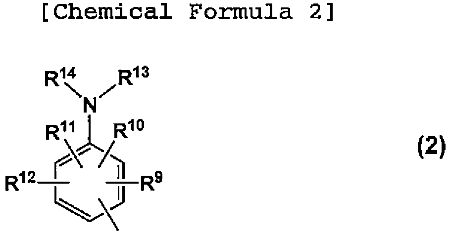
- R 5 to R 8 each independently represent a hydrogen atom, a phenyl group, a naphthyl group, a pyridyl group, a pyrimidinyl group, a pyridazinyl group, a pyrazinyl group, a furanyl group, a pyrrolyl group, a pyrazolyl group, an imidazolyl group, a thienyl group (These groups may be substituted with a halogen atom, a nitro group, a cyano group, a hydroxyl group, a thiol group, a phosphoric acid group, a sulfonic acid group, a carboxyl group, a C1-C20 alkoxy group, a C1-C20 thioalkoxy group, a C1-C20 alkyl group, a C1-C20 haloalkyl group, a C3-C20 cycloalkyl group, a
- R 9 to R 12 each independently represent a hydrogen atom, a halogen atom, a nitro group, a cyano group, a hydroxyl group, a thiol group, a phosphoric acid group, a sulfonic acid group, a carboxyl group, a C1-C20 alkoxy group, a C1-C20 thioalkoxy group, a C1-C20 alkyl group, a C1-C20 haloalkyl group, a C3-C20 cycloalkyl group, a C6-C20 bicycloalkyl group, a C2-C20 alkenyl group, a C2-C20 alkynyl group, a C6-C20 aryl group, a C7-C20 aralkyl group, or a C1-C20 acyl group; and R 13 and R 14 each independently represent a phenyl group, a naphthyl group,
- halogen atom the C1-C20 alkoxy group, C1-C20 thioalkoxy group, C1-C20 alkyl group, C1-C20 haloalkyl group, C3-C20 cycloalkyl group, C6-C20 bicycloalkyl group, C2-C20 alkenyl group, C2-C20 alkynyl group, C6-C20 aryl group, C7-C20 aralkyl group, and C1-C20 acyl group in R 5 to R 14 include the same or similar groups to the above-mentioned.
- R 5 and R 7 are optimally both hydrogen atoms
- R 6 and R 8 are optimally both phenyl groups, from the viewpoint of enhancing the solubility of the aryldiamine derivative in solvents and enhancing the uniformity of the thin film obtained.
- aryldiamine derivative that can be used preferably include, but are not limited to, the following compounds (formulas (1-1) to (1-4)).
- aryldiamine derivative represented by the formula (1) a commercialized one may be used, or one produced by a known method using a benzidine, diaminoterfenyl or the like as a starting material may be used. In either case, it is preferable to use an aryldiamine derivative purified by recrystallization or a vapor deposition method, prior to preparation of the composition for an anode buffer layer.
- an aryldiamine derivative purified by recrystallization or a vapor deposition method, prior to preparation of the composition for an anode buffer layer.
- a purified aryldiamine derivative it is possible to enhance more the characteristics of an OPV element provided with the thin film obtained from the composition.
- 1,4-dioxane, tetrahydrofuran and the like can be used as a solvent.
- the molecular weight of the aryldiamine derivative represented by the formula (1) is not particularly limited. Taking conductivity into consideration, the molecular weight is normally at least 200, preferably at least 300, as a lower limit. In consideration of enhancement of solubility in solvents, the molecular weight is up to 5000, preferably up to 2000, as an upper limit.
- the aryldiamine derivative represented by the formula (1) one compound (in other words, the degree of dispersion of molecular weight distribution is one) selected from the aryldiamine derivatives represented by the formula (1) may be used solely, or two or more compounds selected from the aryldiamine derivatives represented by the formula (1) may be used in combination.
- the electron-accepting dopant substance which is another component contained in the composition for an anode buffer layer of the present invention is not specifically restricted, so long as it is soluble in at least one solvent used in the composition for an anode buffer layer.
- the electron-accepting dopant substance include: inorganic strong acids such as hydrogen chloride, sulfuric acid, nitric acid, and phosphoric acid; Lewis acids such as aluminum(III) chloride (AlCl 3 ), titanium(IV) tetrachloride (TiCl 4 ), boron tribromide (BBr 3 ), boron trifluoride ether complex (BF 3 ⁇ OEt 2 ), iron(III) chloride (FeCl 3 ), copper(II) chloride (CuCl 2 ), antimony(V) pentachloride (SbCl 5 ), arsenic(V) pentafluoride (AsF 5 ), hosphorus pentafluoride (PF 5 ), and tris(4-bromophenyl)aluminum hexachloroantimonate (TBPAH); organic strong acids such as benzenesulfonic acid, tosic acid, camphorsulfonic acid, hydroxybenzen
- arylsulfonic acid compounds preferred are arylsulfonic acid compounds, and particularly preferred are the arylsulfonic acid compounds represented by the formula (3).
- letter X represents O
- letter A represents a naphthalene ring or an anthracene ring
- letter B represents a perfluorobiphenyl group having a valence of 2 to 4
- letter 1 represents the number of sulfonic acid groups bonded to the letter A and is an integer satisfying 1 ⁇ 1 ⁇ 4
- letter q represents the number of bonds of the letter B and the letter X and is an integer satisfying 2 to 4.
- arylsulfonic acid compounds which can be used preferably include, but are not limited to, the following compound (formula (3-1)).
- high-solvency solvents capable of dissolving the aryldiamine derivative and the electron-accepting dopant substance therein can be used.
- the high-solvency solvents may be used either singly or as a mixture of two or more of them, and the amount thereof used can be 5% by weight to 100% by weight based on the total weight of the solvent or solvents used in the composition.
- high-solvency solvents examples include N-methylformamide, N,N-dimethylformamide, N,N-diethylformamide, N-methylacetamide, N,N-dimethylacetamide, N-methylpyrrolidone, and 1,3-dimethyl-2-imidazolidinone.
- N-methylformamide N,N-dimethylformamide, N,N-diethylformamide, N-methylacetamide, and N,N-dimethylacetamide which are amide solvents, and more preferred is N,N-dimethylacetamide.
- the charge-transporting substance and the electron-accepting dopant substance are both preferably in the state of being completely dissolved or uniformly dispersed in the above-mentioned organic solvent. From the viewpoint of obtaining, with good reproducibility, a buffer layer giving an organic thin film solar cell having a high conversion efficiency, it is more preferable that these substances are completely dissolved in the above-mentioned organic solvent.
- composition for an anode buffer layer of the present invention preferably contains at least one high-viscosity organic solvent that has a viscosity of 10 mPa ⁇ s to 200 mPa ⁇ s, particularly 35 mPa ⁇ s to 150 mPa ⁇ s at 25°C and has a boiling point of 50°C to 300°C, particularly 150°C to 250°C at normal pressure.
- the high-viscosity organic solvent is not specifically restricted, and examples thereof include cyclohexanol, ethylene glycol, 1,3-octylene glycol, diethylene glycol, dipropylene glycol, triethylene glycol, tripropylene glycol, 1,3-butanediol, 2,3-butanediol, 1,4-butanediol, propylene glycol, and hexylene glycol.
- the addition ratio of the high-viscosity organic solvent based on the total amount of the solvents used in the composition of the present invention is preferably within such a range that precipitation of solids does not occur.
- the addition ratio is preferably 5% by weight to 80% by weight, so long as precipitation of solids does not occur.
- control of surface tension of solvent, control of polarity, and control of boiling point can be mixed in a proportion of 1% by weight to 90% by weight, preferably 1% by weight to 50% by weight, based on the total weight of the solvents used in the composition.
- Such a solvent examples include, but are not limited to, butyl cellosolve, diethylene glycol diethyl ether, diethylene glycol dimethyl ether, diethylene glycol monoethyl ether acetate, diethylene glycol monobutyl ether acetate, dipropylene glycol monomethyl ether, propylene glycol monomethyl ether, propylene glycol monomethyl ether acetate, ethyl carbitol, diacetone alcohol, ⁇ -butyrolactone, ethyl lactate, and n-hexyl acetate.
- butyl cellosolve diethylene glycol diethyl ether, diethylene glycol dimethyl ether, diethylene glycol monoethyl ether acetate, diethylene glycol monobutyl ether acetate, dipropylene glycol monomethyl ether, propylene glycol monomethyl ether, propylene glycol monomethyl ether acetate, ethyl carbitol, diacetone alcohol
- composition for an anode buffer layer of the present invention desirably contains an organosilane compound, from the viewpoint of enhancing the conversion efficiency of the solar cell obtained.
- organosilane compound examples include trialkoxysilanes, dialkoxysilanes, etc., among which preferred are aryltrialkoxysilanes, aryldialkoxysilanes, fluorine atom-containing trialkoxysilanes, and fluorine atom-containing dialkoxysilanes, and more preferred are the silane compounds represented by the formula (S1) or (S2).
- C1-C6 fluoroalkyl group examples include trifluoromethyl group, 2,2,2-trifluoroethyl group, 1,1,2,2,2-pentafluoroethyl group, 3,3,3-trifluoropropyl group, 2,2,3,3,3-pentafluoropropyl group, 1,1,2,2,3,3,3-heptafluoropropyl group, 4,4,4-trifluorobutyl group, 3,3,4,4,4-pentafluorobutyl group, 2,2,3,3,4,4,4-heptafluorobutyl group, and 1,1,2,2,3,3,4,4,4-nonafluorobutyl group.
- dialkoxysilane compounds include dimethyldimethoxysilane, dimethyldiethoxysilane, methylethyldimethoxysilane, diethyldimethoxysilane, diethyldiethoxysilane, methylpropyldimethoxysilane, methylpropyldiethoxysilane, diisopropyldimethoxysilane, phenylmethyldimethoxysilane, vinylmethyldimethoxysilane, 3-glycidoxypropylmethyldimethoxysilane, 3-glycidoxypropylmethyldiethoxysilane, 3-(3,4-epoxycyclohexyl)ethylmethyldimethoxysilane, 3-methacryloxypropylmethyldimethoxysilane, 3-methacryloxypropylmethyldiethoxysilane, 3-mercaptopropylmethyldimethoxysilane, ⁇ -aminopropylmethyldiethoxysilane,
- trialkoxysilane compounds include methyltrimethoxysilane, methyltriethoxysilane, ethyltrimethoxysilane, ethyltriethoxysilane, propyltrimethoxysilane, propyltriethoxysilane, butyltrimethoxysilane, butyltriethoxysilane, pentyltrimethoxysilane, pentyltriethoxysilane, heptyltrimethoxysilane, heptyltriethoxysilane, octyltrimethoxysilane, octyltriethoxysilane, dodecyltrimethoxysilane, dodecyltriethoxysilane, hexadecyltrimethoxysilane, hexadecyltriethoxysilane, octadecyltrimethoxysilane,
- the content of the organosilane compound is normally about 0.1% by weight to 200% by weight, preferably 1% by weight to 50% by weight, and more preferably 5% by weight to 20% by weight, based on the charge-transporting substance and the electron-accepting dopant substance in the composition of the present invention.
- the concentration of solids in the composition of the present invention is set, as required, taking the viscosity, surface tension and the like of the composition, the thickness of the thin film to be produced, etc. into account.
- the solids concentration is normally about 0.1% by weight to 10.0% by weight, preferably 0.5% by weight to 5.0% by weight, and more preferably 1.0% by weight to 3.0% by weight.
- solids means other components than the organic solvent that constitute the composition for an anode buffer layer.
- the amount-of-material (mol) ratio between the charge-transporting substance and the electron-accepting dopant substance is set, as required, taking the charge-transporting property to be exhibited, the kinds of the charge-transporting substance and the like into account.
- the amount-of-material (mol) ratio of the electron-accepting dopant substance to the charge-transporting substance is normally from 0.1 to 10, preferably from 0.5 to 5.0, and more preferably from 0.5 to 3.0.
- the viscosity of the composition for an anode buffer layer used in the present invention is controlled, as required, taking the thickness and the like of the thin film to be produced and the solids concentration into account and according to the coating method.
- the viscosity is normally about 0.1 mPa ⁇ s to 50 mPa ⁇ s at 25°C.
- the charge-transporting substance, the electron-accepting dopant substance, and the organic solvent in an arbitrary order, so long as the solids are uniformly dissolved or dispersed in the solvent.
- a method of dissolving the aryldiamine derivative in the organic solvent and then dissolving the electron-accepting dopant substance in the resulting solution a method of dissolving the electron-accepting dopant substance in the organic solvent and then dissolving the aryldiamine derivative in the resulting solution, and a method of mixing the aryldiamine derivative and the electron-accepting dopant substance and then putting the mixture into the organic solvent to dissolve the mixture in the organic solvent, can all be adopted, so long as the solids are uniformly dissolved or dispersed in the organic solvent.
- the preparation of the composition is normally conducted in an inert gas atmosphere at normal temperature and normal pressure
- the preparation may be carried out in the atmospheric air (in the presence of oxygen) or with heating, so long as such problems as decomposition of the compounds in the composition or a large change in composition would not occur.
- An anode buffer layer of the present invention can be formed by coating an anode of an organic thin film solar cell with the composition for an anode buffer layer described above and baking the composition.
- an optimum method may be adopted from among various wet process methods such as a drop casting method, a spin coating method, a blade coating method, a dip coating method, a roll coating method, a bar coating method, a die coating method, an ink jet method, and a printing method (relief, intaglio, lithography, and screen printing), taking the viscosity and surface tension of the composition, the thickness of the thin film desired, etc. into account.
- wet process methods such as a drop casting method, a spin coating method, a blade coating method, a dip coating method, a roll coating method, a bar coating method, a die coating method, an ink jet method, and a printing method (relief, intaglio, lithography, and screen printing), taking the viscosity and surface tension of the composition, the thickness of the thin film desired, etc. into account.
- the coating is normally conducted in an inert gas atmosphere at normal temperature and normal pressure, the coating may be carried out in the atmospheric air (in the presence of oxygen) or with heating, so long as problems as decomposition of the compounds in the composition or a large change in composition would not occur.
- the film thickness is normally preferably about 5 nm to 200 nm.
- Examples of a method for changing the film thickness include a method in which the concentration of solids in the composition is changed, and a method in which the coating amount at the time of coating is changed.
- anode material there can be used metal oxides such as indium tin oxide (ITO) and indium zinc oxide (IZO), and highly charge-transporting organic compounds such as polythiophene derivatives and polyaniline derivatives.
- metal oxides such as indium tin oxide (ITO) and indium zinc oxide (IZO)
- highly charge-transporting organic compounds such as polythiophene derivatives and polyaniline derivatives.
- transparent substrate there can be used substrates formed from glass or transparent resin.
- a method for forming a layer of the anode material is selected, as required, according to the properties of the anode material. Normally, either a dry process (a vapor deposition method) using a sublimable compound or a wet process (particularly, a spin coating method or a slit coating method) using a varnish containing the charge-transporting compound is adopted.
- the transparent electrode commercialized ones can also be used preferably.
- a substrate having been subjected to a smoothing treatment it is preferable to use a substrate having been subjected to a smoothing treatment.
- the method of producing the organic thin film solar cell of the present invention does not include the step of forming the anode layer.
- the transparent electrode to be used is preferably washed with a detergent, an alcohol, or pure water before put to use.
- a detergent an alcohol, or pure water
- an anode substrate is preferably subjected to a surface treatment such as a UV ozone treatment, and an oxygen-plasma treatment immediately before put to use (in the case where the anode material has an organic matter as a main constituent, such a surface treatment may be omitted).
- the buffer layer is formed on the layer of the anode material by use of the composition of the present invention.
- An active layer may be a laminate of an n layer which is a thin film composed of an n-type semiconductor material and a p layer which is a thin film composed of a p-type semiconductor material, or may be a non-laminate thin film composed of a mixture of these materials.
- n-type semiconductor material examples include fullerenes, [6,6]-phenyl-C 61 -butyric acid methyl ester (PC 61 BM), and [6,6]-phenyl-C 71 -butyric acid methyl ester (PC 71 BM).
- examples of the p-type semiconductor material include polymers including a thiophene skeleton in a main chain thereof such as regioregular poly(3-hexylthiophene) (P3HT), PTB7 (formula (4)), PDTP-DFBT (formula (5)), and thienothiophene unit-containing polymers described in JP-A 2009-158921 and WO 2010/008672 , phthalocyanines such as CuPC and ZnPC, and porphyrins such as tetrabenzoporphyrin.
- P3HT regioregular poly(3-hexylthiophene)
- PTB7 formula (4)
- PDTP-DFBT formula (5)
- thienothiophene unit-containing polymers described in JP-A 2009-158921 and WO 2010/008672
- phthalocyanines such as CuPC and ZnPC
- porphyrins such as tetra
- PC 61 BM and PC 71 BM are preferable as the n-type material, whereas the polymers including a thiophene skeleton in a main chain thereof such as PTB7 are preferable as the p-type material.
- a thiophene skeleton in a main chain represents a divalent aromatic ring consisting only of thiophene or a divalent condensed aromatic ring including at least one thiophene, such as thienothiophene, benzothiophene, dibenzothiophene, benzodithiophene, naphthothiophene, naphtodithiophene, anthrathiophene, and anthradithiophene, and these may be substituted with a substituent group represented by the above-mentioned R 1 to R 8 .
- a method for forming the active layer is selected, as required, according to the properties of the n-type semiconductor material or p-type semiconductor material. Normally, either a dry process (particularly, a vapor deposition method) using a sublimable compound or a wet process (particularly, a spin coating method or a slit coating method) using a varnish containing the material is adopted.
- a dry process particularly, a vapor deposition method
- a wet process particularly, a spin coating method or a slit coating method
- letter m and letter n each indicate the number of recurring units and represent a positive integer.
- a cathode buffer layer may be formed between the active layer and a cathode layer, for such purposes as achieving a higher charge movement efficiency.
- Examples of a material for forming the cathode buffer layer include lithium oxide (Li 2 O), magnesium oxide (MgO), alumina (Al 2 O 3 ), lithium fluoride (LiF), magnesium fluoride (MgF 2 ), and strontium fluoride (SrF 2 ).
- a method for forming the cathode buffer layer is selected, as required, according to the properties of the material. Normally, either a dry process (particularly, a vapor deposition method) using a sublimable compound or a wet process (particularly, a spin coating method or a slit coating method) using a varnish containing the material is adopted.
- Examples of a cathode material include aluminum, magnesium-silver alloy, aluminum-lithium alloy, lithium, sodium, potassium, cesium, calcium, barium, silver, and gold.
- a plurality of cathode materials can be used in a laminated state or a mixed state.
- the method for forming the cathode buffer layer is selected, as required, according to the properties of the material. Normally, a dry process (particularly, a vapor deposition method) is adopted.
- a carrier block layer may be provided between arbitrary layers, for such purposes as controlling rectification properties of a photocurrent.
- Examples of a material for forming the carrier block layer include titanium oxide, and zinc oxide.
- a method for forming the carrier block layer is selected, as required, according to the properties of the material. Normally, where a sublimable compound is used, a vapor deposition method is adopted. Where a varnish in which the material is dissolved is used, either a spin coating method or a slit coating method is adopted.
- the OPV element produced by the above-exemplified method may be again introduced into a glove box and is subjected to a sealing operation in an atmosphere of an inert gas such as nitrogen, for preventing the element from being deteriorated due to the atmospheric air.
- the OPV element in the sealed state can be made to exhibit the function as a solar cell, or can be put to measurement of solar cell characteristics.
- Examples of the sealing method include a method in which a recessed-type glass substrate with a UV-curable resin adhered to an end portion is adhered to a film formation surface side of the organic thin film solar cell element in an inert gas atmosphere, and the resin is cured by irradiation with UV rays, and a method in which film sealing type sealing is conducted by such a technique as sputtering in vacuum.
- the light yellow solution obtained was filtered through a syringe filter having a pore diameter of 0.2 ⁇ m, to obtain a composition for anode buffer layer B2.
- the light yellow solution obtained was filtered through a syringe filter having a pore diameter of 0.2 ⁇ m, to obtain a composition for anode buffer layer B3.
- the light brown solution obtained was filtered through a syringe filter having a pore diameter of 0.2 ⁇ m, to obtain a composition for anode buffer layer B4.
- the light brown solution obtained was filtered through a syringe filter having a pore diameter of 0.2 ⁇ m, to obtain a composition for anode buffer layer B5.
- PEDOT/PSS (Clevios P VP CH8000, manufactured by Heraeus) was filtered through a syringe filter having a pore diameter of 0.45 ⁇ m, to obtain a composition for anode buffer layer C1.
- a glass substrate measuring 20 mm by 20 mm on which an ITO transparent conductor layer to be positive electrode was patterned in a 2 mm by 20 mm stripe pattern was subjected to a UV/ozone treatment for 15 minutes, and was coated with the composition for anode buffer layer B1 by a spin coating method.
- the glass substrate was heated by use of a hot plate at 50°C for five minutes and further at 230°C for 20 minutes, to form a buffer layer having a thickness of 30 nm.
- the solution A1 was dripped onto the buffer layer formed, a film was formed by a spin coating method, and heating was conducted using a hot plate at 80°C for 30 minutes, to form an active layer having a thickness of 90 nm.
- the substrate formed with the organic semiconductor layer and a mask for cathode were placed in a vacuum vapor deposition apparatus, the apparatus was evacuated to a vacuum degree of up to 1 ⁇ 10 -3 Pa, and an aluminum layer to be a negative electrode was vapor deposited in a thickness of 80 nm by a resistance heating method.
- An OPV element was fabricated by the same method as in Example 1, except that the composition for anode buffer layer B2 was used in place of the composition for anode buffer layer B1.
- a glass substrate measuring 20 mm by 20 mm on which an ITO transparent conductor layer to be a positive electrode was patterned in a 2 mm by 20 mm stripe pattern was subjected to a UV/ozone treatment for 15 minutes, and was then coated with the composition for anode buffer layer B1 prepared on the substrate by a spin coating method.
- This glass substrate was heated by use of a hot plate at 50°C for five minutes and further at 230° C for 20 minutes, to form a buffer layer having a thickness of 30 nm.
- the solution A2 was dripped onto the buffer layer formed, and a film was formed by a spin coating method.
- the substrate formed with the organic semiconductor layer and a mask for cathode were placed in a vacuum vapor deposition apparatus, the apparatus was evacuated to a vacuum degree of up to 1 ⁇ 10 -3 Pa, and an aluminum layer to be a negative electrode was vapor deposited in a thickness of 80 nm by a resistance heating method.
- An OPV element was fabricated by the same method as in Example 3, except that the composition for anode buffer layer B2 was used in place of the composition for anode buffer layer B1.
- An OPV element was fabricated by the same method as in Example 3, except that the composition for active layer A3 was used in place of the composition for active layer A2.
- An OPV element was fabricated by the same method as in Example 3, except that the composition for active layer A3 was used in place of the composition for active layer A2 and that the composition for anode buffer layer B3 was used in place of the composition for anode buffer layer B1.
- An OPV element was fabricated by the same method as in Example 3, except that the composition for anode buffer layer B3 was used in place of the composition for anode buffer layer B1.
- An OPV element was fabricated by the same method as in Example 3, except that the composition for anode buffer layer B4 was used in place of the composition for anode buffer layer B1.
- An OPV element was fabricated by the same method as in Example 3, except that the composition for anode buffer layer B5 was used in place of the composition for anode buffer layer B1.
- An OPV element was fabricated by the same method as in Example 1, except that the composition for anode buffer layer C1 was used in place of the composition for anode buffer layer B1 and that heating at 150°C for 20 minutes was performed in place of the heating at 230°C for 20 minutes.
- An OPV element was fabricated by the same method as in Example 3, except that the composition for anode buffer layer C1 was used in place of the composition for anode buffer layer B1 and that heating at 150°C for 20 minutes was performed in place of the heating at 230°C for 20 minutes.
- An OPV element was fabricated by the same method as in Example 3, except that the composition for active layer A3 was used in place of the composition for active layer A2, the composition for anode buffer layer C1 was used in place of the composition for anode buffer layer B1, and heating at 150°C for 20 minutes was conducted in place of the heating at 230°C for 20 minutes.
- the OPV elements fabricated were put to evaluation of short-circuit current density (Jsc [mA/cm 2 ]), open-circuit voltage (Voc [V]), fill factor (FF), and photoelectric conversion efficiency (PCE [%]).
- the evaluation results in the case where the solution A1 was used as the composition for active layer are set forth in Table 1
- the evaluation results in the case where the solution A2 was used are set forth in Table 2
- the evaluation results in the case where the solution A3 was used (Examples 5 and 6 and Comparative Example 3) are set forth in Table 3.
- the evaluation results in the case where the composition of the composition for anode buffer layer was changed (Examples 4, 7, 8, and 9) are set forth in Table 4.
- the OPV elements provided with the thin film obtained from the composition for anode buffer layer of the present invention as the anode buffer layer showed high photoelectric conversion efficiencies (PCE) as compared to the OPV elements provided with the thin film obtained from PEDOT/PSS in general use as the anode buffer layer, independently of the kind of the composition for active layer.
- PCE photoelectric conversion efficiencies
- composition for anode buffer layer of the present invention OPV elements with excellent photoelectric conversion characteristics can be produced.
Landscapes
- Chemical & Material Sciences (AREA)
- Organic Chemistry (AREA)
- Engineering & Computer Science (AREA)
- Materials Engineering (AREA)
- Physics & Mathematics (AREA)
- Spectroscopy & Molecular Physics (AREA)
- Health & Medical Sciences (AREA)
- Polymers & Plastics (AREA)
- Medicinal Chemistry (AREA)
- Chemical Kinetics & Catalysis (AREA)
- Electromagnetism (AREA)
- Nanotechnology (AREA)
- Power Engineering (AREA)
- Microelectronics & Electronic Packaging (AREA)
- Photovoltaic Devices (AREA)
- Organic Low-Molecular-Weight Compounds And Preparation Thereof (AREA)
Abstract
Description
- The present invention relates to a composition for an anode buffer layer of an organic thin film solar cell, and an organic thin film solar cell.
- Organic thin film solar cells are solar cell elements using organic matter for an active layer and as a charge-transporting substance, among which the dye-sensitized solar cell developed by M. Gratzel and the organic thin film solar cell developed by C.W. Tang are well known (Non-patent Documents 1 and 2).
- Both types of solar cells have different characteristic properties from those of the inorganic solar cells which are the main stream at present, in such points that they are light in weight, are thin films, can be made to be flexible, and can be produced on a roll-to-roll basis, so that they are expected to form a new market.
- Among others, the organic thin film solar cells (organic photovoltaics; hereinafter abbreviated to OPV) have been drawing great attention, since they are characterized in that they are at least free of electrolytes and free of heavy metal compounds, and since a photoelectric conversion efficiency (hereinafter abbreviated to PCE) of 10.6% has recently been reported by a group of UCLA et al. (Non-patent Document 3).
- In recent years, utilization of renewable energy has been advocated, and developments thereof have been being accelerated. In regard of the OPV, investigations have been under way for putting devices of energy harvesting and the like into practical use in their early stages. Besides, the following further wider ranges of use of the OPV devices are expected.
- However, PEDOT/PSS often used as an anode buffer layer in the OPV is prepared as an aqueous dispersion, and it is very difficult to remove water completely or to inhibit reabsorption of water; therefore, there is a problem that water is liable to accelerate deterioration of the OPV element. In addition, since the PEDOT/PSS aqueous dispersion is liable to show aggregation of solids, there are problems that defects are liable to be generated in the coating film, that the coating apparatus is susceptible to clogging or corrosion, etc.; thus, there have been problems yet to be solved, also in the mass production process.
-
- Non-Patent Document 1: Nature, vol. 353, 737-740 (1991)
- Non-Patent Document 2: Appl. Phys. Lett., Vol. 48, 183-185 (1986)
- Non-Patent Document 3: Nature Photonics Vol. 6, 153-161 (2012)
- The present invention has been made in consideration of the above-mentioned circumstances. Accordingly, it is an object of the present invention to provide a composition that gives a thin film suitable for an anode buffer layer of an organic thin film solar cell.
- In order to achieve the above object, the present inventors earnestly made investigations. As a result of the investigations, the inventors found out that a composition containing an aryldiamine derivative and an electron-accepting dopant substance is completely dissolved in an organic solvent to form a uniform solution, and that when a thin film obtained from the uniform solution is used as an anode buffer layer of an organic thin film solar cell, it is thereby possible to obtain an organic thin film solar cell having excellent photoelectric conversion characteristics. Based on the findings, the inventors have completed the present invention.
- Accordingly, the present invention provides:
- 1. A composition for an anode buffer layer of an organic thin film solar cell, the composition including: a charge-transporting substance including an aryldiamine derivative represented by the formula (1); an electron-accepting dopant substance; and an organic solvent;

- 2. The composition for an anode buffer layer of an organic thin film solar cell according to the above paragraph 1, wherein R5 and R7 are hydrogen atoms, and R6 and R8 are phenyl groups;
- 3. The composition for an anode buffer layer of an organic thin film solar cell according to the above paragraph 1 or 2, wherein n is 2 or 3;
- 4. The composition for an anode buffer layer of an organic thin film solar cell according to any one of the above paragraphs 1 to 3, wherein the electron-accepting dopant substance includes an arylsulfonic acid compound;
- 5. The composition for an anode buffer layer of an organic thin film solar cell according to the above paragraph 4, wherein the arylsulfonic acid compound is represented by the formula (3);

- 6. The composition for an anode buffer layer of an organic thin film solar cell according to the above paragraph 5, wherein the letter X represents O, and the letter A represents a naphthalene ring or an anthracene ring;
- 7. The composition for an anode buffer layer of an organic thin film solar cell according to any one of the above paragraphs 1 to 6, including an organosilane compound;
- 8. An organic thin film solar cell including: an anode buffer layer produced from the composition for an anode buffer layer of an organic thin film solar cell according to any one of the above paragraphs 1 to 7; and an active layer provided in such a manner as to make contact with the anode buffer layer;
- 9. The organic thin film solar cell according to the above paragraph 8, wherein the active layer includes a fullerene derivative;
- 10. The organic thin film solar cell according to the above paragraph 8, wherein the active layer includes a polymer including a thiophene skeleton in a main chain; and
- 11. The organic thin film solar cell according to the above paragraph 8, wherein the active layer includes a fullerene derivative and a polymer including a thiophene skeleton in a main chain.
- The composition of the present invention not only can be produced by use of compounds inexpensively available from the market, but also ensures that when a thin film obtained therefrom is used as an anode buffer layer, it is possible to obtain an organic thin film solar cell having an excellent photoelectric conversion efficiency.
- The present invention will be described more in detail below.
- The composition for an anode buffer layer of an organic thin film solar cell of the present invention includes an aryldiamine derivative of the above formula (1), an electron-accepting dopant substance, and an organic solvent.
- R1 to R4 each independently represent a hydrogen atom, a halogen atom, a nitro group, a cyano group, a hydroxyl group, a thiol group, a phosphoric acid group, a sulfonic acid group, a carboxyl group, a C1-C20 alkoxy group, a C1-C20 thioalkoxy group, a C1-C20 alkyl group, a C1-C20 haloalkyl group, a C3-C20 cycloalkyl group, a C6-C20 bicycloalkyl group, a C2-C20 alkenyl group, a C2-C20 alkynyl group, a C6-C20 aryl group, a C7-C20 aralkyl group, or a C1-C20 acyl group.
- Here, examples of the halogen atom include fluorine, chlorine, bromine, and iodine atoms.
- Specific examples of the C1-C20 alkoxy group include methoxy group, ethoxy group, n-propoxy group, i-propoxy group, c-propoxy group, n-butoxy group, i-butoxy group, s-butoxy group, t-butoxy group, n-pentoxy group, n-hexoxy group, n-heptyloxy group, n-octyloxy group, n-nonyloxy group, n-decyloxy group, n-undecyloxy group, n-dodecyloxy group, n-tridecyloxy group, n-tetradecyloxy group, n-pentadecyloxy group, n-hexadecyloxy group, n-heptadecyloxy group, n-octadecyloxy group, n-nonadecyloxy group, and n-eicosanyloxy group.
- Specific examples of the C1-C20 thioalkoxy (alkylthio) group include methylthio group, ethylthio group, n-propylthio group, isopropylthio group, n-butylthio group, isobutylthio group, s-butylthio group, t-butylthio group, n-pentylthio group, n-hexylthio group, n-heptylthio group, n-octylthio group, n-nonylthio group, n-decylthio group, n-undecylthio group, n-dodecylthio group, n-tridecylthio group, n-tetradecylthio group, n-pentadecylthio group, n-hexdecylthio group, n-heptadecylthio group, n-octadecylthio group, n-nonadecylthio group, and n-eicosanylthio group.
- Specific examples of the C1-C20 alkyl group include methyl group, ethyl group, n-propyl group, isopropyl group, n-butyl group, isobutyl group, s-butyl group, t-butyl group, n-pentyl group, n-hexyl group, n-heptyl group, n-octyl group, n-nonyl group, n-decyl group, n-undecyl group, n-dodecyl group, n-tridecyl group, n-tetradecyl group, n-pentadecyl group, n-hexadecyl group, n-heptadecyl group, n-octadecyl group, n-nonadecyl group, and n-eicosanyl group.
- Examples of the C1-C20 haloalkyl group include those groups obtained by replacing at least one of the hydrogen atoms of the above C1-C20 alkyl groups with a halogen atom. Among these groups, preferred are fluoroalkyl groups, and more preferred are perfluoroalkyl groups.
- Specific examples of them include fluoromethyl group, difluoromethyl group, trifluoromethyl group, pentafluoroethyl group, 2,2,2-trifluoroethyl group, heptafluoropropyl group, 2,2,3,3,3-pentafluoropropyl group, 2,2,3,3-tetrafluoropropyl group, 2,2,2-trifluoro-1-(trifluoromethyl)ethyl group, nonafluorobutyl group, 4,4,4-trifluorobutyl group, undecafluoropentyl group, 2,2,3,3,4,4,5,5,5-nonafluoropentyl group, 2,2,3,3,4,4,5,5-octafluoropentyl group, tridecafluorohexyl group, 2,2,3,3,4,4,5,5,6,6,6-undecafluorohexyl group, 2,2,3,3,4,4,5,5,6,6-decafluorohexyl group, and 3,3,4,4,5,5,6,6,6-nonafluorohexyl group.
- Specific examples of the C3-C20 cycloalkyl group include cyclopropyl group, cyclobutyl group, cyclopentyl group, cyclohexyl group, cycloheptyl group, cyclooctyl group, and cyclononyl group.
- Specific examples of the C6-C20 bicycloalkyl group include bicyclopropyl group, bicyclobutyl group, bicyclopentyl group, bicyclohexyl group, bicycloheptyl group, bicyclooctyl group, and bicyclononyl group.
- Specific examples of the C2-C20 alkenyl group include vinyl group, 1-propenyl group, 2-propenyl group, 1-methyl-2-propenyl group, 2-butenyl group, 3-butenyl group, 2-pentenyl group, 3-pentenyl group, 4-pentenyl group, 2-hexenyl group, 3-hexenyl group, 4-hexenyl group, 5-hexenyl group, 6-heptenyl group, 7-octenyl group, 3,7-dimethyl-6-octenyl group, 8-nonenyl group, 9-decenyl group, 10-undecenyl group, 11-dedecenyl group, 12-tridecenyl group, 13-tetradecenyl group, 14-pentadecenyl group, 15-hexadecenyl group, 16-heptadecenyl group, 17-octadecenyl group, 18-nonadecenyl group, and 19-eicosenyl group.
- Specific examples of the C2-C20 alkynyl group include ethynyl group, 1-propynyl group, 2-propynyl group, 1-methyl-2-propynyl group, 2-butynyl group, 3-butynyl group, 2-pentynyl group, 3-pentynyl group, 4-pentynyl group, 2-hexynyl group, 3-hexynyl group, 4-hexynyl group, 5-hexynyl group, 6-heptynyl group, 7-octynyl group, 3,7-dimethyl-6-octynyl group, 8-nonynyl group, 9-decynyl group, 10-undecynyl group, 11-dodecynyl group, 12-tridecynyl group, 13-tetradecynyl group, 14-pentadecynyl group, 15-hexadecenyl group, 16-heptadecynyl group, 17-octadecynyl group, 18-nonadecynyl group, and 19-eicosynyl group.
- Specific examples of the C6-C20 aryl group include phenyl group, α-naphthyl group, β-naphthyl group, anthryl group, phenanthrenyl group, o-biphenylyl group, m-biphenylyl group, and p-biphenylyl group.
- Specific examples of the C7-C20 aralkyl group include benzyl group, phenylethyl group, phenylpropyl group, naphthylmethyl group, naphthylethyl group, and naphthylpropyl group.
- Specific examples of the C1-C20 acyl group include formyl group, acetyl group, propionyl group, butyryl group, isobutyryl group, valeryl group, isovaleryl group, and benzoyl group.
- Among these, R1 to R4 are preferably each a hydrogen atom, a halogen atom, a C1-C4 alkyl group, a C1-C4 perfluoroalkyl group, or a C1-C4 alkoxy group, and are optimally all hydrogen atoms, from the viewpoint of enhancing the solubility of the aryldiamine derivative in solvents and enhancing the uniformity of the thin film obtained.
- R5 to R8 each independently represent a hydrogen atom, a phenyl group, a naphthyl group, a pyridyl group, a pyrimidinyl group, a pyridazinyl group, a pyrazinyl group, a furanyl group, a pyrrolyl group, a pyrazolyl group, an imidazolyl group, a thienyl group (These groups may be substituted with a halogen atom, a nitro group, a cyano group, a hydroxyl group, a thiol group, a phosphoric acid group, a sulfonic acid group, a carboxyl group, a C1-C20 alkoxy group, a C1-C20 thioalkoxy group, a C1-C20 alkyl group, a C1-C20 haloalkyl group, a C3-C20 cycloalkyl group, a C6-C20 bicycloalkyl group, a C2-C20 alkenyl group, a C2-C20 alkynyl group, a C6-C20 aryl group, a C7-C20 aralkyl group, or a C1-C20 acyl group.), or a group represented by the above formula (2), with at least one of R5 to R8 being a hydrogen atom.
- In the above formula (2), R9 to R12 each independently represent a hydrogen atom, a halogen atom, a nitro group, a cyano group, a hydroxyl group, a thiol group, a phosphoric acid group, a sulfonic acid group, a carboxyl group, a C1-C20 alkoxy group, a C1-C20 thioalkoxy group, a C1-C20 alkyl group, a C1-C20 haloalkyl group, a C3-C20 cycloalkyl group, a C6-C20 bicycloalkyl group, a C2-C20 alkenyl group, a C2-C20 alkynyl group, a C6-C20 aryl group, a C7-C20 aralkyl group, or a C1-C20 acyl group; and R13 and R14 each independently represent a phenyl group, a naphthyl group, an anthryl group, a pyridyl group, a pyrimidinyl group, a pyridazinyl group, a pyrazinyl group, a furanyl group, a pyrrolyl group, a pyrazolyl group, an imidazolyl group, a thienyl group (These groups may be bonded to each other to form a ring, and may be substituted with a halogen atom, a nitro group, a cyano group, a hydroxyl group, a thiol group, a phosphoric acid group, a sulfonic acid group, a carboxyl group, a C1-C20 alkoxy group, a C1-C20 thioalkoxy group, a C1-C20 alkyl group, a C1-C20 haloalkyl group, a C3-C20 cycloalkyl group, a C6-C20 bicycloalkyl group, a C2-C20 alkenyl group, a C2-C20 alkynyl group, a C6-C20 aryl group, a C7-C20 aralkyl group, or a C1-C20 acyl group.).
- Note that specific examples of the halogen atom, the C1-C20 alkoxy group, C1-C20 thioalkoxy group, C1-C20 alkyl group, C1-C20 haloalkyl group, C3-C20 cycloalkyl group, C6-C20 bicycloalkyl group, C2-C20 alkenyl group, C2-C20 alkynyl group, C6-C20 aryl group, C7-C20 aralkyl group, and C1-C20 acyl group in R5 to R14 include the same or similar groups to the above-mentioned.
- Among these, R5 and R7 are optimally both hydrogen atoms, and R6 and R8 are optimally both phenyl groups, from the viewpoint of enhancing the solubility of the aryldiamine derivative in solvents and enhancing the uniformity of the thin film obtained.
- In the present invention, specific examples of the aryldiamine derivative that can be used preferably include, but are not limited to, the following compounds (formulas (1-1) to (1-4)).

- As the aryldiamine derivative represented by the formula (1), a commercialized one may be used, or one produced by a known method using a benzidine, diaminoterfenyl or the like as a starting material may be used. In either case, it is preferable to use an aryldiamine derivative purified by recrystallization or a vapor deposition method, prior to preparation of the composition for an anode buffer layer. By using a purified aryldiamine derivative, it is possible to enhance more the characteristics of an OPV element provided with the thin film obtained from the composition. In the case of purification by recrystallization, for example, 1,4-dioxane, tetrahydrofuran and the like can be used as a solvent.
- The molecular weight of the aryldiamine derivative represented by the formula (1) is not particularly limited. Taking conductivity into consideration, the molecular weight is normally at least 200, preferably at least 300, as a lower limit. In consideration of enhancement of solubility in solvents, the molecular weight is up to 5000, preferably up to 2000, as an upper limit.
- In the composition for an anode buffer layer of the present invention, as the aryldiamine derivative represented by the formula (1), one compound (in other words, the degree of dispersion of molecular weight distribution is one) selected from the aryldiamine derivatives represented by the formula (1) may be used solely, or two or more compounds selected from the aryldiamine derivatives represented by the formula (1) may be used in combination.
- The electron-accepting dopant substance which is another component contained in the composition for an anode buffer layer of the present invention is not specifically restricted, so long as it is soluble in at least one solvent used in the composition for an anode buffer layer.
- Specific examples of the electron-accepting dopant substance include: inorganic strong acids such as hydrogen chloride, sulfuric acid, nitric acid, and phosphoric acid; Lewis acids such as aluminum(III) chloride (AlCl3), titanium(IV) tetrachloride (TiCl4), boron tribromide (BBr3), boron trifluoride ether complex (BF3·OEt2), iron(III) chloride (FeCl3), copper(II) chloride (CuCl2), antimony(V) pentachloride (SbCl5), arsenic(V) pentafluoride (AsF5), hosphorus pentafluoride (PF5), and tris(4-bromophenyl)aluminum hexachloroantimonate (TBPAH); organic strong acids such as benzenesulfonic acid, tosic acid, camphorsulfonic acid, hydroxybenzenesulfonic acid, 5-sulfosalicylic acid, dodecylbenzenesulfonic acid, polystyrenesulfonic acid, 1,4-benzodioxanedisulfonic acid compounds described in
WO 2005/000832 , arylsulfonic acid compounds described inWO 2006/025342 , and dinonylnaphthalenesulfonic acid compounds described inJP-A 2005-108828 WO 2010/058777 . These respective substances may be used in combination. - Among them, preferred are arylsulfonic acid compounds, and particularly preferred are the arylsulfonic acid compounds represented by the formula (3).

- In the present invention, specific examples of the arylsulfonic acid compounds which can be used preferably include, but are not limited to, the following compound (formula (3-1)).

- As the organic solvent for use in preparing the composition for an anode buffer layer, high-solvency solvents capable of dissolving the aryldiamine derivative and the electron-accepting dopant substance therein can be used. The high-solvency solvents may be used either singly or as a mixture of two or more of them, and the amount thereof used can be 5% by weight to 100% by weight based on the total weight of the solvent or solvents used in the composition.
- Examples of such high-solvency solvents include N-methylformamide, N,N-dimethylformamide, N,N-diethylformamide, N-methylacetamide, N,N-dimethylacetamide, N-methylpyrrolidone, and 1,3-dimethyl-2-imidazolidinone.
- Among these, preferred are N-methylformamide, N,N-dimethylformamide, N,N-diethylformamide, N-methylacetamide, and N,N-dimethylacetamide which are amide solvents, and more preferred is N,N-dimethylacetamide.
- The charge-transporting substance and the electron-accepting dopant substance are both preferably in the state of being completely dissolved or uniformly dispersed in the above-mentioned organic solvent. From the viewpoint of obtaining, with good reproducibility, a buffer layer giving an organic thin film solar cell having a high conversion efficiency, it is more preferable that these substances are completely dissolved in the above-mentioned organic solvent.
- The composition for an anode buffer layer of the present invention preferably contains at least one high-viscosity organic solvent that has a viscosity of 10 mPa·s to 200 mPa·s, particularly 35 mPa·s to 150 mPa·s at 25°C and has a boiling point of 50°C to 300°C, particularly 150°C to 250°C at normal pressure.
- The high-viscosity organic solvent is not specifically restricted, and examples thereof include cyclohexanol, ethylene glycol, 1,3-octylene glycol, diethylene glycol, dipropylene glycol, triethylene glycol, tripropylene glycol, 1,3-butanediol, 2,3-butanediol, 1,4-butanediol, propylene glycol, and hexylene glycol.
- The addition ratio of the high-viscosity organic solvent based on the total amount of the solvents used in the composition of the present invention is preferably within such a range that precipitation of solids does not occur. The addition ratio is preferably 5% by weight to 80% by weight, so long as precipitation of solids does not occur.
- Further, for purposes such as enhancement of wetting property in regard of a surface to be treated, control of surface tension of solvent, control of polarity, and control of boiling point, other solvent capable of imparting film flatness at the time of a heat treatment can be mixed in a proportion of 1% by weight to 90% by weight, preferably 1% by weight to 50% by weight, based on the total weight of the solvents used in the composition.
- Examples of such a solvent include, but are not limited to, butyl cellosolve, diethylene glycol diethyl ether, diethylene glycol dimethyl ether, diethylene glycol monoethyl ether acetate, diethylene glycol monobutyl ether acetate, dipropylene glycol monomethyl ether, propylene glycol monomethyl ether, propylene glycol monomethyl ether acetate, ethyl carbitol, diacetone alcohol, γ-butyrolactone, ethyl lactate, and n-hexyl acetate.
- The composition for an anode buffer layer of the present invention desirably contains an organosilane compound, from the viewpoint of enhancing the conversion efficiency of the solar cell obtained.
- Examples of the organosilane compound include trialkoxysilanes, dialkoxysilanes, etc., among which preferred are aryltrialkoxysilanes, aryldialkoxysilanes, fluorine atom-containing trialkoxysilanes, and fluorine atom-containing dialkoxysilanes, and more preferred are the silane compounds represented by the formula (S1) or (S2).
-
RSi(OCH3)3 (S1)
RSi(OC2H5)3 (S2)
(In the formulas, letter R represents a C1-C6 fluoroalkyl group.) - Specific examples of the C1-C6 fluoroalkyl group include trifluoromethyl group, 2,2,2-trifluoroethyl group, 1,1,2,2,2-pentafluoroethyl group, 3,3,3-trifluoropropyl group, 2,2,3,3,3-pentafluoropropyl group, 1,1,2,2,3,3,3-heptafluoropropyl group, 4,4,4-trifluorobutyl group, 3,3,4,4,4-pentafluorobutyl group, 2,2,3,3,4,4,4-heptafluorobutyl group, and 1,1,2,2,3,3,4,4,4-nonafluorobutyl group.
- Specific examples of the dialkoxysilane compounds include dimethyldimethoxysilane, dimethyldiethoxysilane, methylethyldimethoxysilane, diethyldimethoxysilane, diethyldiethoxysilane, methylpropyldimethoxysilane, methylpropyldiethoxysilane, diisopropyldimethoxysilane, phenylmethyldimethoxysilane, vinylmethyldimethoxysilane, 3-glycidoxypropylmethyldimethoxysilane, 3-glycidoxypropylmethyldiethoxysilane, 3-(3,4-epoxycyclohexyl)ethylmethyldimethoxysilane, 3-methacryloxypropylmethyldimethoxysilane, 3-methacryloxypropylmethyldiethoxysilane, 3-mercaptopropylmethyldimethoxysilane, γ-aminopropylmethyldiethoxysilane, N-(2-aminoethyl)aminopropylmethyldimethoxysilane, and 3,3,3-trifluoropropylmethyldimethoxysilane.
- Specific examples of the trialkoxysilane compounds include methyltrimethoxysilane, methyltriethoxysilane, ethyltrimethoxysilane, ethyltriethoxysilane, propyltrimethoxysilane, propyltriethoxysilane, butyltrimethoxysilane, butyltriethoxysilane, pentyltrimethoxysilane, pentyltriethoxysilane, heptyltrimethoxysilane, heptyltriethoxysilane, octyltrimethoxysilane, octyltriethoxysilane, dodecyltrimethoxysilane, dodecyltriethoxysilane, hexadecyltrimethoxysilane, hexadecyltriethoxysilane, octadecyltrimethoxysilane, octadecyltriethoxysilane, phenyltrimethoxysilane, phenyltriethoxysilane, vinyltrimethoxysilane, vinyltriethoxysilane, γ-aminopropyltrimethoxysilane, 3-aminopropyltriethoxysilane, γ-glycidoxypropyltrimethoxysilane, 3-glycidoxypropyltriethoxysilane, γ-methacryloxypropyltrimethoxysilane, γ-methacryloxypropyltriethoxysilane, triethoxy(4-(trifluoromethyl)phenyl)silane, dodecyltriethoxysilane, 3,3,3-trifluoropropyltrimethoxysilane, (triethoxysilyl)cyclohexane, perfluorooctylethyltriethoxysilane, triethoxyfluorosilane, tridecafluoro-1,1,2,2-tetrahydrooctyltriethoxysilane, 3-(heptafluoroisopropoxy)propyltriethoxysilane, heptadecafluoro-1,1,2,2-tetrahydrodecyltriethoxysilane, triethoxy-2-thienylsilane, and 3-(triethoxysilyl)furan.
- In the present invention, the content of the organosilane compound is normally about 0.1% by weight to 200% by weight, preferably 1% by weight to 50% by weight, and more preferably 5% by weight to 20% by weight, based on the charge-transporting substance and the electron-accepting dopant substance in the composition of the present invention.
- The concentration of solids in the composition of the present invention is set, as required, taking the viscosity, surface tension and the like of the composition, the thickness of the thin film to be produced, etc. into account. The solids concentration is normally about 0.1% by weight to 10.0% by weight, preferably 0.5% by weight to 5.0% by weight, and more preferably 1.0% by weight to 3.0% by weight.
- Note that the solids means other components than the organic solvent that constitute the composition for an anode buffer layer.
- In addition, the amount-of-material (mol) ratio between the charge-transporting substance and the electron-accepting dopant substance is set, as required, taking the charge-transporting property to be exhibited, the kinds of the charge-transporting substance and the like into account. The amount-of-material (mol) ratio of the electron-accepting dopant substance to the charge-transporting substance is normally from 0.1 to 10, preferably from 0.5 to 5.0, and more preferably from 0.5 to 3.0.
- Besides, the viscosity of the composition for an anode buffer layer used in the present invention is controlled, as required, taking the thickness and the like of the thin film to be produced and the solids concentration into account and according to the coating method. The viscosity is normally about 0.1 mPa·s to 50 mPa·s at 25°C.
- In preparing the composition of the present invention, it is possible to mix the charge-transporting substance, the electron-accepting dopant substance, and the organic solvent in an arbitrary order, so long as the solids are uniformly dissolved or dispersed in the solvent. Specifically, for example, a method of dissolving the aryldiamine derivative in the organic solvent and then dissolving the electron-accepting dopant substance in the resulting solution, a method of dissolving the electron-accepting dopant substance in the organic solvent and then dissolving the aryldiamine derivative in the resulting solution, and a method of mixing the aryldiamine derivative and the electron-accepting dopant substance and then putting the mixture into the organic solvent to dissolve the mixture in the organic solvent, can all be adopted, so long as the solids are uniformly dissolved or dispersed in the organic solvent.
- In addition, while the preparation of the composition is normally conducted in an inert gas atmosphere at normal temperature and normal pressure, the preparation may be carried out in the atmospheric air (in the presence of oxygen) or with heating, so long as such problems as decomposition of the compounds in the composition or a large change in composition would not occur.
- An anode buffer layer of the present invention can be formed by coating an anode of an organic thin film solar cell with the composition for an anode buffer layer described above and baking the composition.
- At the time of coating, an optimum method may be adopted from among various wet process methods such as a drop casting method, a spin coating method, a blade coating method, a dip coating method, a roll coating method, a bar coating method, a die coating method, an ink jet method, and a printing method (relief, intaglio, lithography, and screen printing), taking the viscosity and surface tension of the composition, the thickness of the thin film desired, etc. into account.
- While the coating is normally conducted in an inert gas atmosphere at normal temperature and normal pressure, the coating may be carried out in the atmospheric air (in the presence of oxygen) or with heating, so long as problems as decomposition of the compounds in the composition or a large change in composition would not occur.
- The film thickness is normally preferably about 5 nm to 200 nm. Examples of a method for changing the film thickness include a method in which the concentration of solids in the composition is changed, and a method in which the coating amount at the time of coating is changed.
- A method of producing an organic thin film solar cell by use of the composition of the present invention will be described below.
- As an anode material, there can be used metal oxides such as indium tin oxide (ITO) and indium zinc oxide (IZO), and highly charge-transporting organic compounds such as polythiophene derivatives and polyaniline derivatives. Besides, as a transparent substrate, there can be used substrates formed from glass or transparent resin.
- A method for forming a layer of the anode material (anode layer) is selected, as required, according to the properties of the anode material. Normally, either a dry process (a vapor deposition method) using a sublimable compound or a wet process (particularly, a spin coating method or a slit coating method) using a varnish containing the charge-transporting compound is adopted.
- In addition, as the transparent electrode, commercialized ones can also be used preferably. In this case, from the viewpoint of enhancing the yield of the element, it is preferable to use a substrate having been subjected to a smoothing treatment. In the case where a commercialized transparent electrode is used, the method of producing the organic thin film solar cell of the present invention does not include the step of forming the anode layer.
- The transparent electrode to be used is preferably washed with a detergent, an alcohol, or pure water before put to use. For example, an anode substrate is preferably subjected to a surface treatment such as a UV ozone treatment, and an oxygen-plasma treatment immediately before put to use (in the case where the anode material has an organic matter as a main constituent, such a surface treatment may be omitted).
- According to the above-mentioned method, the buffer layer is formed on the layer of the anode material by use of the composition of the present invention.
- An active layer may be a laminate of an n layer which is a thin film composed of an n-type semiconductor material and a p layer which is a thin film composed of a p-type semiconductor material, or may be a non-laminate thin film composed of a mixture of these materials.
- Examples of the n-type semiconductor material include fullerenes, [6,6]-phenyl-C61-butyric acid methyl ester (PC61BM), and [6,6]-phenyl-C71-butyric acid methyl ester (PC71BM). On the other hand, examples of the p-type semiconductor material include polymers including a thiophene skeleton in a main chain thereof such as regioregular poly(3-hexylthiophene) (P3HT), PTB7 (formula (4)), PDTP-DFBT (formula (5)), and thienothiophene unit-containing polymers described in
JP-A 2009-158921 WO 2010/008672 , phthalocyanines such as CuPC and ZnPC, and porphyrins such as tetrabenzoporphyrin. - Among these, PC61BM and PC71BM are preferable as the n-type material, whereas the polymers including a thiophene skeleton in a main chain thereof such as PTB7 are preferable as the p-type material.
- Note that "a thiophene skeleton in a main chain" represents a divalent aromatic ring consisting only of thiophene or a divalent condensed aromatic ring including at least one thiophene, such as thienothiophene, benzothiophene, dibenzothiophene, benzodithiophene, naphthothiophene, naphtodithiophene, anthrathiophene, and anthradithiophene, and these may be substituted with a substituent group represented by the above-mentioned R1 to R8.
- A method for forming the active layer is selected, as required, according to the properties of the n-type semiconductor material or p-type semiconductor material. Normally, either a dry process (particularly, a vapor deposition method) using a sublimable compound or a wet process (particularly, a spin coating method or a slit coating method) using a varnish containing the material is adopted.

- If necessary, a cathode buffer layer may be formed between the active layer and a cathode layer, for such purposes as achieving a higher charge movement efficiency.
- Examples of a material for forming the cathode buffer layer include lithium oxide (Li2O), magnesium oxide (MgO), alumina (Al2O3), lithium fluoride (LiF), magnesium fluoride (MgF2), and strontium fluoride (SrF2).
- A method for forming the cathode buffer layer is selected, as required, according to the properties of the material. Normally, either a dry process (particularly, a vapor deposition method) using a sublimable compound or a wet process (particularly, a spin coating method or a slit coating method) using a varnish containing the material is adopted.
- Examples of a cathode material include aluminum, magnesium-silver alloy, aluminum-lithium alloy, lithium, sodium, potassium, cesium, calcium, barium, silver, and gold. A plurality of cathode materials can be used in a laminated state or a mixed state.
- The method for forming the cathode buffer layer is selected, as required, according to the properties of the material. Normally, a dry process (particularly, a vapor deposition method) is adopted.
- When necessary, a carrier block layer may be provided between arbitrary layers, for such purposes as controlling rectification properties of a photocurrent.
- Examples of a material for forming the carrier block layer include titanium oxide, and zinc oxide.
- A method for forming the carrier block layer is selected, as required, according to the properties of the material. Normally, where a sublimable compound is used, a vapor deposition method is adopted. Where a varnish in which the material is dissolved is used, either a spin coating method or a slit coating method is adopted.
- The OPV element produced by the above-exemplified method may be again introduced into a glove box and is subjected to a sealing operation in an atmosphere of an inert gas such as nitrogen, for preventing the element from being deteriorated due to the atmospheric air. The OPV element in the sealed state can be made to exhibit the function as a solar cell, or can be put to measurement of solar cell characteristics.
- Examples of the sealing method include a method in which a recessed-type glass substrate with a UV-curable resin adhered to an end portion is adhered to a film formation surface side of the organic thin film solar cell element in an inert gas atmosphere, and the resin is cured by irradiation with UV rays, and a method in which film sealing type sealing is conducted by such a technique as sputtering in vacuum.
- The present invention will be described more specifically below by showing Examples and Comparative Examples, but the present invention is not to be restricted to the following Examples.
-
- (1) NMR Apparatus: ECX-300, manufactured by JEOL Ltd. Solvent for measurement: dimethyl sulfoxide-d6, manufactured by Junsei Chemical Co., Ltd.
- (2) Glove box: VAC Glove Box System, manufactured by Yamahachi & Co., Ltd.
- (3) Vapor deposition apparatus: Vacuum Vapor Deposition Apparatus, manufactured by Aoyama Engineering K.K.
- (4) Solar simulator: OTENTOSUN-III, manufactured by Bunkoukeiki K.K.; AM 1.5G filter, radiation intensity: 100 mW/cm2
- (5) Source measure unit: 2612A, manufactured by Keithley Instruments K.K.
- Into a sample bottle containing 40 mg of regioregular poly(3-hexylthiophene) (product name: lisicon (registered trademark) SP-001, manufactured by Merck) and 32 mg of PC61BM (product name: nanom spectra E100, manufactured by Frontier Carbon Corporation), was added 2.0 mL of chlorobenzene, followed by stirring on a hot plate at 80°C for 15 hours, to obtain solution A1 (composition for active layer).
- Into a sample bottle containing 20 mg of PTB7 (manufactured by 1-Material) and 30 mg of PC61BM (product name: nanom spectra E100, manufactured by Frontier Carbon Corporation), was added 2.0 mL of chlorobenzene, followed by stirring on a hot plate at 80°C for 15 hours. After this solution was let cool to room temperature, 60 µL of 1,8-diiodooctane (manufactured by Tokyo Chemical Industry Co., Ltd.) was added thereto, followed by stirring, to obtain solution A2 (composition for active layer).
- Into a sample bottle containing 20 mg of PDTP-DFBT (manufactured by 1-Material) and 30 mg of PC61BM (product name: nanom spectra E100, manufactured by Frontier Carbon Corporation), was added 2.0 mL of chlorobenzene, followed by stirring on a hot plate at 80°C for 15 hours. After this solution was let cool to room temperature, 60 µL of 1,8-diiodooctane (manufactured by Tokyo Chemical Industry Co., Ltd.) was added thereto, followed by stirring, to obtain solution A3 (composition for active layer).
- To a mixture of 132.1 mg (0.393 mmol) of N,N'-diphenylbenzidine (manufactured by Tokyo Chemical Industry Co., Ltd., the same applies hereinafter) and 177.2 mg (0.196 mmol) of an arylsulfonic acid compound represented by the above formula (3-1) synthesized according to the method described in
WO 2006/025342 , was added 5.0 g of N,N-dimethylacetamide, followed by stirring at room temperature with irradiation with ultrasonic waves, to effect dissolution. Further, 5.0 g of cyclohexanol was added to the resulting solution, followed by stirring, to obtain a light yellow solution. The light yellow solution obtained was filtered through a syringe filter having a pore diameter of 0.2 µm, to obtain a composition for anode buffer layer B1. - To 10.0 g of N,N-dimethylacetamide were added 0.717 mg (3.61 mmol) of phenyltrimethoxysilane (manufactured by Shin-Etsu Chemical Co., Ltd.) and 0.394 mg (1.81 mmol) of 3,3,3-trifluoropropyltrimethoxysilane (manufactured by Shin-Etsu Chemical Co., Ltd.), followed by stirring at room temperature, to obtain a silane compound solution S1.
- To 10.0 g of 1,3-dimethyl-2-imidazolidinone were added 0.717 mg (3.61 mmol) of phenyltrimethoxysilane (manufactured by Shin-Etsu Chemical Co., Ltd.) and 0.394 mg (1.81 mmol) of 3,3,3-trifluoropropyltrimethoxysilane (manufactured by Shin-Etsu Chemical Co., Ltd.), followed by stirring at room temperature, to obtain a silane compound solution S2.
- To a mixture of 92.5 mg (0.275 mmol) of N,N'-diphenylbenzidine and 186.1 mg (0.206 mmol) of an arylsulfonic acid compound represented by the above formula (3-1) synthesized according to the method described in
WO 2006/025342 , was added 4.72 g of N,N-dimethylacetamide, followed by stirring at room temperature with irradiation with ultrasonic waves to effect dissolution. Further, 5.0 g of cyclohexanol was added to the resulting solution, followed by stirring, and then 0.31 g of the silane compound solution S1 was added thereto, to obtain a light yellow solution. - The light yellow solution obtained was filtered through a syringe filter having a pore diameter of 0.2 µm, to obtain a composition for anode buffer layer B2.
- To a mixture of 61.0 mg (0.181 mmol) of N,N'-diphenylbenzidine and 122.8 mg (0.136 mmol) of an arylsulfonic acid compound represented by the above formula (3-1) synthesized according to the method described in
WO 2006/025342 , was added 4.82 g of N,N-dimethylacetamide, followed by stirring at room temperature with irradiation with ultrasonic waves to effect dissolution. Further, 5.0 g of cyclohexanol was added to the resulting solution, followed by stirring, and then 0.21 g of the silane compound solution S1 was added thereto, to obtain a light yellow solution. - The light yellow solution obtained was filtered through a syringe filter having a pore diameter of 0.2 µm, to obtain a composition for anode buffer layer B3.
- To a mixture of 61.0 mg (0.181 mmol) of N,N'-diphenylbenzidine and 122.8 mg (0.136 mmol) of an arylsulfonic acid compound represented by the above formula (3-1) synthesized according to the method described in
WO 2006/025342 , were added 3.15 g of N,N-dimethylacetamide and 1.67 g of 2,3-butanediol, followed by stirring at room temperature with irradiation with ultrasonic waves to effect dissolution. Further, 5.0 g of cyclohexanol was added to the resulting solution, followed by stirring, and then 0.21 g of the silane compound solution S1 was added thereto, to obtain a light brown solution. - The light brown solution obtained was filtered through a syringe filter having a pore diameter of 0.2 µm, to obtain a composition for anode buffer layer B4.
- To a mixture of 61.0 mg (0.181 mmol) of N,N'-diphenylbenzidine and 122.8 mg (0.136 mmol) of an arylsulfonic acid compound represented by the above formula (3-1) synthesized according to the method described in
WO 2006/025342 , were added 3.15 g of 1,3-dimethyl-2-imidazolidinone and 1.67 g of propylene glycol, followed by stirring at room temperature with irradiation with ultrasonic waves to effect dissolution. Further, 5.0 g of cyclohexanol was added to the resulting solution, followed by stirring, and then 0.21 g of the silane compound solution S2 was added thereto, to obtain a light brown solution. - The light brown solution obtained was filtered through a syringe filter having a pore diameter of 0.2 µm, to obtain a composition for anode buffer layer B5.
- PEDOT/PSS (Clevios P VP CH8000, manufactured by Heraeus) was filtered through a syringe filter having a pore diameter of 0.45 µm, to obtain a composition for anode buffer layer C1.
- A glass substrate measuring 20 mm by 20 mm on which an ITO transparent conductor layer to be positive electrode was patterned in a 2 mm by 20 mm stripe pattern was subjected to a UV/ozone treatment for 15 minutes, and was coated with the composition for anode buffer layer B1 by a spin coating method. The glass substrate was heated by use of a hot plate at 50°C for five minutes and further at 230°C for 20 minutes, to form a buffer layer having a thickness of 30 nm.
- Thereafter, in a glove box flushed with an inert gas, the solution A1 was dripped onto the buffer layer formed, a film was formed by a spin coating method, and heating was conducted using a hot plate at 80°C for 30 minutes, to form an active layer having a thickness of 90 nm.
- Next, the substrate formed with the organic semiconductor layer and a mask for cathode were placed in a vacuum vapor deposition apparatus, the apparatus was evacuated to a vacuum degree of up to 1×10⁻³ Pa, and an aluminum layer to be a negative electrode was vapor deposited in a thickness of 80 nm by a resistance heating method.
- Finally, heating was conducted using a hot plate at 135°C for 10 minutes, to fabricate an OPV element wherein the area of intersection of the stripe-patterned ITO layer and the aluminum layer was 2 mm by 2 mm.
- An OPV element was fabricated by the same method as in Example 1, except that the composition for anode buffer layer B2 was used in place of the composition for anode buffer layer B1.
- A glass substrate measuring 20 mm by 20 mm on which an ITO transparent conductor layer to be a positive electrode was patterned in a 2 mm by 20 mm stripe pattern was subjected to a UV/ozone treatment for 15 minutes, and was then coated with the composition for anode buffer layer B1 prepared on the substrate by a spin coating method. This glass substrate was heated by use of a hot plate at 50°C for five minutes and further at 230° C for 20 minutes, to form a buffer layer having a thickness of 30 nm.
- Thereafter, in a glove box flushed with an inert gas, the solution A2 was dripped onto the buffer layer formed, and a film was formed by a spin coating method.
- Next, the substrate formed with the organic semiconductor layer and a mask for cathode were placed in a vacuum vapor deposition apparatus, the apparatus was evacuated to a vacuum degree of up to 1×10⁻³ Pa, and an aluminum layer to be a negative electrode was vapor deposited in a thickness of 80 nm by a resistance heating method.
- Finally, heating was conducted using a hot plate at 90°C for 10 minutes, to fabricate an OPV element wherein the area of intersection of the striped ITO layer and the aluminum layer was 2 mm by 2 mm.
- An OPV element was fabricated by the same method as in Example 3, except that the composition for anode buffer layer B2 was used in place of the composition for anode buffer layer B1.
- An OPV element was fabricated by the same method as in Example 3, except that the composition for active layer A3 was used in place of the composition for active layer A2.
- An OPV element was fabricated by the same method as in Example 3, except that the composition for active layer A3 was used in place of the composition for active layer A2 and that the composition for anode buffer layer B3 was used in place of the composition for anode buffer layer B1.
- An OPV element was fabricated by the same method as in Example 3, except that the composition for anode buffer layer B3 was used in place of the composition for anode buffer layer B1.
- An OPV element was fabricated by the same method as in Example 3, except that the composition for anode buffer layer B4 was used in place of the composition for anode buffer layer B1.
- An OPV element was fabricated by the same method as in Example 3, except that the composition for anode buffer layer B5 was used in place of the composition for anode buffer layer B1.
- An OPV element was fabricated by the same method as in Example 1, except that the composition for anode buffer layer C1 was used in place of the composition for anode buffer layer B1 and that heating at 150°C for 20 minutes was performed in place of the heating at 230°C for 20 minutes.
- An OPV element was fabricated by the same method as in Example 3, except that the composition for anode buffer layer C1 was used in place of the composition for anode buffer layer B1 and that heating at 150°C for 20 minutes was performed in place of the heating at 230°C for 20 minutes.
- An OPV element was fabricated by the same method as in Example 3, except that the composition for active layer A3 was used in place of the composition for active layer A2, the composition for anode buffer layer C1 was used in place of the composition for anode buffer layer B1, and heating at 150°C for 20 minutes was conducted in place of the heating at 230°C for 20 minutes.
- The OPV elements fabricated were put to evaluation of short-circuit current density (Jsc [mA/cm2]), open-circuit voltage (Voc [V]), fill factor (FF), and photoelectric conversion efficiency (PCE [%]). The evaluation results in the case where the solution A1 was used as the composition for active layer (Examples 1 and 2 and Comparative Example 1) are set forth in Table 1, the evaluation results in the case where the solution A2 was used (Examples 3 and 4 and Comparative Example 2) are set forth in Table 2, and the evaluation results in the case where the solution A3 was used (Examples 5 and 6 and Comparative Example 3) are set forth in Table 3. In addition, the evaluation results in the case where the composition of the composition for anode buffer layer was changed (Examples 4, 7, 8, and 9) are set forth in Table 4.
- Note that the photoelectric conversion efficiency was calculated by the formula of:

[Table 1] Jsc Voc FF PCE Example 1 8.3 0.56 0.58 2.7 Example 2 8.5 0.57 0.58 2.8 Comparative Example 1 8.9 0.61 0.43 2.3 [Table 2] Jsc Voc FF PCE Example 3 13.2 0.77 0.58 5.9 Example 4 13.4 0.78 0.61 6.4 Comparative Example 2 12.8 0.79 0.29 2.9 [Table 3] Jsc Voc FF PCE Example 5 9.6 0.72 0.36 2.5 Example 6 10.1 0.74 0.37 2.8 Comparative Example 3 4.2 0.75 0.17 0.5 [Table 4] Jsc Voc FF PCE Example 4 12.5 0.76 0.49 4.6 Example 7 12.6 0.76 0.57 5.5 Example 8 12.6 0.75 0.57 5.5 Example 9 12.7 0.73 0.54 5.0 - As shown in Tables 1 to 4, the OPV elements provided with the thin film obtained from the composition for anode buffer layer of the present invention as the anode buffer layer showed high photoelectric conversion efficiencies (PCE) as compared to the OPV elements provided with the thin film obtained from PEDOT/PSS in general use as the anode buffer layer, independently of the kind of the composition for active layer.
- Thus, it is seen that by use of the composition for anode buffer layer of the present invention, OPV elements with excellent photoelectric conversion characteristics can be produced.
Claims (11)
- A composition for an anode buffer layer of an organic thin film solar cell, the composition comprising:a charge-transporting substance including an aryldiamine derivative represented by the formula (1);an electron-accepting dopant substance; andan organic solvent.{In the formula, R1 to R4 each independently represent a hydrogen atom, a halogen atom, a nitro group, a cyano group, a hydroxyl group, a thiol group, a phosphoric acid group, a sulfonic acid group, a carboxyl group, a C1-C20 alkoxy group, a C1-C20 thioalkoxy group, a C1-C20 alkyl group, a C1-C20 haloalkyl group, a C3-C20 cycloalkyl group, a C6-C20 bicycloalkyl group, a C2-C20 alkenyl group, a C2-C20 alkynyl group, a C6-C20 aryl group, a C7-C20 aralkyl group, or a C1-C20 acyl group,

R5 to R8 each independently represent a hydrogen atom, a phenyl group, a naphthyl group, a pyridyl group, a pyrimidinyl group, a pyridazinyl group, a pyrazinyl group, a furanyl group, a pyrrolyl group, a pyrazolyl group, an imidazolyl group, a thienyl group (These groups may be substituted with a halogen atom, a nitro group, a cyano group, a hydroxyl group, a thiol group, a phosphoric acid group, a sulfonic acid group, a carboxyl group, a C1-C20 alkoxy group, a C1-C20 thioalkoxy group, a C1-C20 alkyl group, a C1-C20 haloalkyl group, a C3-C20 cycloalkyl group, a C6-C20 bicycloalkyl group, a C2-C20 alkenyl group, a C2-C20 alkynyl group, a C6-C20 aryl group, a C7-C20 aralkyl group, or a C1-C20 acyl group.), or a group represented by the formula (2) (Provided that at least one of R5 to R8 is a hydrogen atom.),
R13 and R14 each independently represent a phenyl group, a naphthyl group, an anthryl group, a pyridyl group, a pyrimidinyl group, a pyridazinyl group, a pyrazinyl group, a furanyl group, a pyrrolyl group, a pyrazolyl group, an imidazolyl group, a thienyl group (These groups may be bonded to each other to form a ring, and may be substituted with a halogen atom, a nitro group, a cyano group, a hydroxyl group, a thiol group, a phosphoric acid group, a sulfonic acid group, a carboxyl group, a C1-C20 alkoxy group, a C1-C20 thioalkoxy group, a C1-C20 alkyl group, a C1-C20 haloalkyl group, a C3-C20 cycloalkyl group, a C6-C20 bicycloalkyl group, a C2-C20 alkenyl group, a C2-C20 alkynyl group, a C6-C20 aryl group, a C7-C20 aralkyl group, or a C1-C20 acyl group.)], and
n represents an integer of 2 to 5.} - The composition for an anode buffer layer of an organic thin film solar cell according to claim 1, wherein R5 and R7 are hydrogen atoms, and
R6 and R8 are phenyl groups. - The composition for an anode buffer layer of an organic thin film solar cell according to claim 1 or 2, wherein n is 2 or 3.
- The composition for an anode buffer layer of an organic thin film solar cell according to any one of claims 1 to 3, wherein the electron-accepting dopant substance includes an arylsulfonic acid compound.
- The composition for an anode buffer layer of an organic thin film solar cell according to claim 4, wherein the arylsulfonic acid compound is represented by the formula (3).
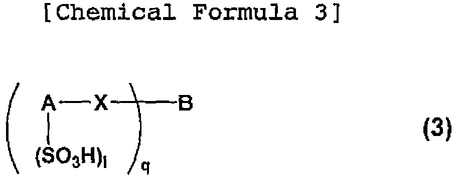
- The composition for an anode buffer layer of an organic thin film solar cell according to claim 5, wherein the letter X represents O, and the letter A represents a naphthalene ring or an anthracene ring.
- The composition for an anode buffer layer of an organic thin film solar cell according to any one of claims 1 to 6, comprising an organosilane compound.
- An organic thin film solar cell comprising:an anode buffer layer produced from the composition for an anode buffer layer of an organic thin film solar cell according to any one of claims 1 to 7; andan active layer provided in such a manner as to make contact with the anode buffer layer.
- The organic thin film solar cell according to claim 8, wherein the active layer includes a fullerene derivative.
- The organic thin film solar cell according to claim 8, wherein the active layer includes a polymer including a thiophene skeleton in a main chain.
- The organic thin film solar cell according to claim 8, wherein the active layer includes a fullerene derivative and a polymer including a thiophene skeleton in a main chain.
Applications Claiming Priority (2)
| Application Number | Priority Date | Filing Date | Title |
|---|---|---|---|
| JP2013254159 | 2013-12-09 | ||
| PCT/JP2014/082228 WO2015087797A1 (en) | 2013-12-09 | 2014-12-05 | Composition for anode buffer layer of organic thin film solar cell and organic thin film solar cell |
Publications (3)
| Publication Number | Publication Date |
|---|---|
| EP3082171A1 true EP3082171A1 (en) | 2016-10-19 |
| EP3082171A4 EP3082171A4 (en) | 2017-08-09 |
| EP3082171B1 EP3082171B1 (en) | 2022-04-27 |
Family
ID=53371102
Family Applications (1)
| Application Number | Title | Priority Date | Filing Date |
|---|---|---|---|
| EP14870013.1A Active EP3082171B1 (en) | 2013-12-09 | 2014-12-05 | Composition for anode buffer layer of organic thin film solar cell and organic thin film solar cell |
Country Status (7)
| Country | Link |
|---|---|
| US (1) | US10020449B2 (en) |
| EP (1) | EP3082171B1 (en) |
| JP (1) | JP6520718B2 (en) |
| KR (1) | KR102252204B1 (en) |
| CN (1) | CN105934836A (en) |
| TW (1) | TWI623513B (en) |
| WO (1) | WO2015087797A1 (en) |
Cited By (1)
| Publication number | Priority date | Publication date | Assignee | Title |
|---|---|---|---|---|
| EP3544072A4 (en) * | 2016-12-16 | 2019-11-27 | Nissan Chemical Corporation | COMPOSITION FOR COLLECTING LAYER OF ORGANIC PHOTOELECTRIC CONVERSION ELEMENT HOLES |
Families Citing this family (5)
| Publication number | Priority date | Publication date | Assignee | Title |
|---|---|---|---|---|
| KR20180080232A (en) | 2015-11-06 | 2018-07-11 | 닛산 가가쿠 고교 가부시키 가이샤 | Composition for hole-trapping layer of organic photoelectric conversion element |
| US11028277B2 (en) * | 2016-02-03 | 2021-06-08 | Nissan Chemical Corporation | Charge transport varnish |
| CN110692145A (en) * | 2017-05-25 | 2020-01-14 | 日产化学株式会社 | Method for producing charge-transporting thin film |
| US10991842B2 (en) * | 2017-10-23 | 2021-04-27 | Sumitomo Chemical Company, Limited | Photoelectric conversion element |
| GB2589570A (en) * | 2019-11-29 | 2021-06-09 | Sumitomo Chemical Co | Photoactive composition |
Family Cites Families (25)
| Publication number | Priority date | Publication date | Assignee | Title |
|---|---|---|---|---|
| US6416818B1 (en) * | 1998-08-17 | 2002-07-09 | Nanophase Technologies Corporation | Compositions for forming transparent conductive nanoparticle coatings and process of preparation therefor |
| JP3893869B2 (en) * | 2000-10-13 | 2007-03-14 | 富士ゼロックス株式会社 | Organic electroluminescence device |
| TW200504046A (en) | 2003-06-25 | 2005-02-01 | Nissan Chemical Ind Ltd | 1,4-Benzodioxane sulfonic acid compound and use thereof as electron-acceptor material |
| JP5024498B2 (en) * | 2003-09-11 | 2012-09-12 | 日産化学工業株式会社 | Charge transporting varnish, charge transporting thin film, and organic electroluminescence device |
| EP1785413B1 (en) | 2004-08-31 | 2014-01-22 | Nissan Chemical Industries, Ltd. | Arylsulfonic acid compound and use thereof as electron-acceptor material |
| US20070181874A1 (en) * | 2004-12-30 | 2007-08-09 | Shiva Prakash | Charge transport layers and organic electron devices comprising same |
| EP2057701A2 (en) * | 2006-08-24 | 2009-05-13 | E.I. Du Pont De Nemours And Company | Organic electronic devices |
| KR101473294B1 (en) | 2006-09-13 | 2014-12-16 | 닛산 가가쿠 고교 가부시키 가이샤 | Oligoaniline compound and use thereof |
| US8153029B2 (en) * | 2006-12-28 | 2012-04-10 | E.I. Du Pont De Nemours And Company | Laser (230NM) ablatable compositions of electrically conducting polymers made with a perfluoropolymeric acid applications thereof |
| JP4946923B2 (en) * | 2007-03-07 | 2012-06-06 | 三菱化学株式会社 | Organic electroluminescence device |
| US8298444B2 (en) | 2007-04-12 | 2012-10-30 | Nissan Chemical Industries, Ltd. | Oligoaniline compound |
| EP1990847B1 (en) | 2007-05-10 | 2018-06-20 | Novaled GmbH | Use of quinoid bisimidazoles and their derivatives as dopant for doping an organic semi-conductor matrix material |
| JP5359173B2 (en) | 2007-12-05 | 2013-12-04 | 東レ株式会社 | Electron donating organic material for photovoltaic element, photovoltaic element material and photovoltaic element |
| KR100999377B1 (en) * | 2008-06-18 | 2010-12-09 | 한국과학기술원 | Organic based solar cell and manufacturing method thereof |
| CN102149750B (en) | 2008-07-18 | 2014-04-23 | 芝加哥大学 | Semiconducting polymers |
| WO2010041701A1 (en) | 2008-10-09 | 2010-04-15 | 日産化学工業株式会社 | Charge-transporting varnishes |
| CN101397308A (en) * | 2008-11-04 | 2009-04-01 | 东华大学 | POSS hybrid hole-transporting material and preparation method thereof |
| WO2010058777A1 (en) | 2008-11-19 | 2010-05-27 | 日産化学工業株式会社 | Charge transporting material and charge transporting varnish |
| US20100147386A1 (en) * | 2008-11-21 | 2010-06-17 | Plextronics, Inc. | Doped interfacial modification layers for stability enhancement for bulk heterojunction organic solar cells |
| WO2012042623A1 (en) * | 2010-09-29 | 2012-04-05 | 富士通株式会社 | Method for constructing ring network |
| JP2012234959A (en) * | 2011-04-28 | 2012-11-29 | Suminoe Textile Co Ltd | Photovoltaic thread covered with thermoplastic resin, and method for manufacturing the same |
| KR101641674B1 (en) | 2011-09-21 | 2016-07-21 | 닛산 가가쿠 고교 가부시키 가이샤 | Charge-transporting varnish |
| WO2013124029A2 (en) * | 2012-02-22 | 2013-08-29 | Merck Patent Gmbh | Polymers containing dibenzocycloheptene structural units |
| JP2013225436A (en) * | 2012-04-23 | 2013-10-31 | Sony Corp | Organic electroluminescent device, method for manufacturing the same, and electronic apparatus |
| WO2014132834A1 (en) * | 2013-02-26 | 2014-09-04 | 日産化学工業株式会社 | Charge-transporting varnish |
-
2014
- 2014-12-05 EP EP14870013.1A patent/EP3082171B1/en active Active
- 2014-12-05 WO PCT/JP2014/082228 patent/WO2015087797A1/en not_active Ceased
- 2014-12-05 CN CN201480074096.4A patent/CN105934836A/en active Pending
- 2014-12-05 JP JP2015552419A patent/JP6520718B2/en active Active
- 2014-12-05 US US15/102,775 patent/US10020449B2/en active Active
- 2014-12-05 KR KR1020167017592A patent/KR102252204B1/en active Active
- 2014-12-09 TW TW103142853A patent/TWI623513B/en active
Cited By (1)
| Publication number | Priority date | Publication date | Assignee | Title |
|---|---|---|---|---|
| EP3544072A4 (en) * | 2016-12-16 | 2019-11-27 | Nissan Chemical Corporation | COMPOSITION FOR COLLECTING LAYER OF ORGANIC PHOTOELECTRIC CONVERSION ELEMENT HOLES |
Also Published As
| Publication number | Publication date |
|---|---|
| JPWO2015087797A1 (en) | 2017-03-16 |
| CN105934836A (en) | 2016-09-07 |
| WO2015087797A1 (en) | 2015-06-18 |
| TW201538459A (en) | 2015-10-16 |
| KR20160096637A (en) | 2016-08-16 |
| KR102252204B1 (en) | 2021-05-14 |
| US10020449B2 (en) | 2018-07-10 |
| EP3082171A4 (en) | 2017-08-09 |
| EP3082171B1 (en) | 2022-04-27 |
| JP6520718B2 (en) | 2019-05-29 |
| TWI623513B (en) | 2018-05-11 |
| US20160315266A1 (en) | 2016-10-27 |
Similar Documents
| Publication | Publication Date | Title |
|---|---|---|
| EP3082171B1 (en) | Composition for anode buffer layer of organic thin film solar cell and organic thin film solar cell | |
| JP2022153435A (en) | Optical sensor element | |
| EP3373354B1 (en) | Composition for hole trapping layer of organic photoelectric conversion element | |
| EP3413367B1 (en) | Charge transport varnish | |
| US11563176B2 (en) | Composition for hole collecting layer of organic photoelectric conversion element | |
| US11527719B2 (en) | Hole collection layer composition for organic photoelectric conversion element | |
| EP3633749A1 (en) | Method for producing charge transporting thin film | |
| EP4159800A1 (en) | Composition for hole collecting layer of organic photoelectric conversion element |
Legal Events
| Date | Code | Title | Description |
|---|---|---|---|
| PUAI | Public reference made under article 153(3) epc to a published international application that has entered the european phase |
Free format text: ORIGINAL CODE: 0009012 |
|
| 17P | Request for examination filed |
Effective date: 20160704 |
|
| AK | Designated contracting states |
Kind code of ref document: A1 Designated state(s): AL AT BE BG CH CY CZ DE DK EE ES FI FR GB GR HR HU IE IS IT LI LT LU LV MC MK MT NL NO PL PT RO RS SE SI SK SM TR |
|
| AX | Request for extension of the european patent |
Extension state: BA ME |
|
| DAX | Request for extension of the european patent (deleted) | ||
| A4 | Supplementary search report drawn up and despatched |
Effective date: 20170710 |
|
| RIC1 | Information provided on ipc code assigned before grant |
Ipc: C08L 65/00 20060101ALI20170704BHEP Ipc: C08K 3/04 20060101ALI20170704BHEP Ipc: H01L 51/46 20060101AFI20170704BHEP Ipc: C07C 309/43 20060101ALI20170704BHEP Ipc: C07C 211/54 20060101ALI20170704BHEP |
|
| RAP1 | Party data changed (applicant data changed or rights of an application transferred) |
Owner name: NISSAN CHEMICAL CORPORATION |
|
| STAA | Information on the status of an ep patent application or granted ep patent |
Free format text: STATUS: EXAMINATION IS IN PROGRESS |
|
| 17Q | First examination report despatched |
Effective date: 20191212 |
|
| GRAP | Despatch of communication of intention to grant a patent |
Free format text: ORIGINAL CODE: EPIDOSNIGR1 |
|
| STAA | Information on the status of an ep patent application or granted ep patent |
Free format text: STATUS: GRANT OF PATENT IS INTENDED |
|
| INTG | Intention to grant announced |
Effective date: 20210830 |
|
| GRAJ | Information related to disapproval of communication of intention to grant by the applicant or resumption of examination proceedings by the epo deleted |
Free format text: ORIGINAL CODE: EPIDOSDIGR1 |
|
| STAA | Information on the status of an ep patent application or granted ep patent |
Free format text: STATUS: EXAMINATION IS IN PROGRESS |
|
| INTC | Intention to grant announced (deleted) | ||
| GRAP | Despatch of communication of intention to grant a patent |
Free format text: ORIGINAL CODE: EPIDOSNIGR1 |
|
| STAA | Information on the status of an ep patent application or granted ep patent |
Free format text: STATUS: GRANT OF PATENT IS INTENDED |
|
| INTG | Intention to grant announced |
Effective date: 20220111 |
|
| GRAS | Grant fee paid |
Free format text: ORIGINAL CODE: EPIDOSNIGR3 |
|
| GRAA | (expected) grant |
Free format text: ORIGINAL CODE: 0009210 |
|
| STAA | Information on the status of an ep patent application or granted ep patent |
Free format text: STATUS: THE PATENT HAS BEEN GRANTED |
|
| RBV | Designated contracting states (corrected) |
Designated state(s): BE DE FR GB NL |
|
| AK | Designated contracting states |
Kind code of ref document: B1 Designated state(s): BE DE FR GB NL |
|
| REG | Reference to a national code |
Ref country code: GB Ref legal event code: FG4D |
|
| REG | Reference to a national code |
Ref country code: DE Ref legal event code: R096 Ref document number: 602014083466 Country of ref document: DE |
|
| REG | Reference to a national code |
Ref country code: NL Ref legal event code: FP |
|
| REG | Reference to a national code |
Ref country code: DE Ref legal event code: R079 Ref document number: 602014083466 Country of ref document: DE Free format text: PREVIOUS MAIN CLASS: H01L0051460000 Ipc: H10K0085000000 |
|
| REG | Reference to a national code |
Ref country code: DE Ref legal event code: R097 Ref document number: 602014083466 Country of ref document: DE |
|
| PLBE | No opposition filed within time limit |
Free format text: ORIGINAL CODE: 0009261 |
|
| STAA | Information on the status of an ep patent application or granted ep patent |
Free format text: STATUS: NO OPPOSITION FILED WITHIN TIME LIMIT |
|
| 26N | No opposition filed |
Effective date: 20230130 |
|
| P01 | Opt-out of the competence of the unified patent court (upc) registered |
Effective date: 20230522 |
|
| PGFP | Annual fee paid to national office [announced via postgrant information from national office to epo] |
Ref country code: DE Payment date: 20251119 Year of fee payment: 12 |
|
| PGFP | Annual fee paid to national office [announced via postgrant information from national office to epo] |
Ref country code: GB Payment date: 20251119 Year of fee payment: 12 |
|
| PGFP | Annual fee paid to national office [announced via postgrant information from national office to epo] |
Ref country code: NL Payment date: 20251217 Year of fee payment: 12 Ref country code: FR Payment date: 20251119 Year of fee payment: 12 |
|
| PGFP | Annual fee paid to national office [announced via postgrant information from national office to epo] |
Ref country code: BE Payment date: 20251119 Year of fee payment: 12 |