EP3082038A1 - Verfahren, vorrichtung und system zur erzeugung eines massiv parallelisierten, ausführbaren objekts - Google Patents
Verfahren, vorrichtung und system zur erzeugung eines massiv parallelisierten, ausführbaren objekts Download PDFInfo
- Publication number
- EP3082038A1 EP3082038A1 EP15163717.0A EP15163717A EP3082038A1 EP 3082038 A1 EP3082038 A1 EP 3082038A1 EP 15163717 A EP15163717 A EP 15163717A EP 3082038 A1 EP3082038 A1 EP 3082038A1
- Authority
- EP
- European Patent Office
- Prior art keywords
- processing
- subtask
- identified
- elements
- processing elements
- Prior art date
- Legal status (The legal status is an assumption and is not a legal conclusion. Google has not performed a legal analysis and makes no representation as to the accuracy of the status listed.)
- Withdrawn
Links
- 238000000034 method Methods 0.000 title claims abstract description 62
- 238000012545 processing Methods 0.000 claims abstract description 325
- 238000012546 transfer Methods 0.000 claims description 21
- 238000004891 communication Methods 0.000 claims description 7
- 230000008901 benefit Effects 0.000 description 13
- 101100184723 Homo sapiens PMPCA gene Proteins 0.000 description 9
- 102100025321 Mitochondrial-processing peptidase subunit alpha Human genes 0.000 description 9
- 239000000872 buffer Substances 0.000 description 9
- 239000004744 fabric Substances 0.000 description 8
- 230000008569 process Effects 0.000 description 5
- 230000005540 biological transmission Effects 0.000 description 4
- 230000001419 dependent effect Effects 0.000 description 4
- 238000003860 storage Methods 0.000 description 4
- 230000006870 function Effects 0.000 description 3
- XBBRGUHRZBZMPP-UHFFFAOYSA-N 1,2,3-trichloro-4-(2,4,6-trichlorophenyl)benzene Chemical compound ClC1=CC(Cl)=CC(Cl)=C1C1=CC=C(Cl)C(Cl)=C1Cl XBBRGUHRZBZMPP-UHFFFAOYSA-N 0.000 description 2
- RYGMFSIKBFXOCR-UHFFFAOYSA-N Copper Chemical compound [Cu] RYGMFSIKBFXOCR-UHFFFAOYSA-N 0.000 description 2
- 238000004364 calculation method Methods 0.000 description 2
- 229910052802 copper Inorganic materials 0.000 description 2
- 239000010949 copper Substances 0.000 description 2
- 230000014759 maintenance of location Effects 0.000 description 2
- 230000015654 memory Effects 0.000 description 2
- 230000003068 static effect Effects 0.000 description 2
- 238000004458 analytical method Methods 0.000 description 1
- 238000013459 approach Methods 0.000 description 1
- 238000004590 computer program Methods 0.000 description 1
- 238000001152 differential interference contrast microscopy Methods 0.000 description 1
- 238000009826 distribution Methods 0.000 description 1
- 238000004519 manufacturing process Methods 0.000 description 1
- 239000013307 optical fiber Substances 0.000 description 1
- 238000005457 optimization Methods 0.000 description 1
- 230000002093 peripheral effect Effects 0.000 description 1
- 230000008092 positive effect Effects 0.000 description 1
- 230000036316 preload Effects 0.000 description 1
- 238000003672 processing method Methods 0.000 description 1
- 230000009467 reduction Effects 0.000 description 1
Images


Classifications
-
- G—PHYSICS
- G06—COMPUTING; CALCULATING OR COUNTING
- G06F—ELECTRIC DIGITAL DATA PROCESSING
- G06F9/00—Arrangements for program control, e.g. control units
- G06F9/06—Arrangements for program control, e.g. control units using stored programs, i.e. using an internal store of processing equipment to receive or retain programs
- G06F9/46—Multiprogramming arrangements
- G06F9/48—Program initiating; Program switching, e.g. by interrupt
- G06F9/4806—Task transfer initiation or dispatching
- G06F9/4843—Task transfer initiation or dispatching by program, e.g. task dispatcher, supervisor, operating system
- G06F9/485—Task life-cycle, e.g. stopping, restarting, resuming execution
-
- G—PHYSICS
- G06—COMPUTING; CALCULATING OR COUNTING
- G06F—ELECTRIC DIGITAL DATA PROCESSING
- G06F8/00—Arrangements for software engineering
- G06F8/40—Transformation of program code
- G06F8/41—Compilation
- G06F8/44—Encoding
- G06F8/443—Optimisation
-
- G—PHYSICS
- G06—COMPUTING; CALCULATING OR COUNTING
- G06F—ELECTRIC DIGITAL DATA PROCESSING
- G06F8/00—Arrangements for software engineering
- G06F8/40—Transformation of program code
- G06F8/41—Compilation
- G06F8/45—Exploiting coarse grain parallelism in compilation, i.e. parallelism between groups of instructions
- G06F8/451—Code distribution
-
- G—PHYSICS
- G06—COMPUTING; CALCULATING OR COUNTING
- G06F—ELECTRIC DIGITAL DATA PROCESSING
- G06F8/00—Arrangements for software engineering
- G06F8/40—Transformation of program code
- G06F8/41—Compilation
- G06F8/45—Exploiting coarse grain parallelism in compilation, i.e. parallelism between groups of instructions
- G06F8/456—Parallelism detection
-
- G—PHYSICS
- G06—COMPUTING; CALCULATING OR COUNTING
- G06F—ELECTRIC DIGITAL DATA PROCESSING
- G06F8/00—Arrangements for software engineering
- G06F8/40—Transformation of program code
- G06F8/41—Compilation
- G06F8/45—Exploiting coarse grain parallelism in compilation, i.e. parallelism between groups of instructions
- G06F8/457—Communication
-
- G—PHYSICS
- G06—COMPUTING; CALCULATING OR COUNTING
- G06F—ELECTRIC DIGITAL DATA PROCESSING
- G06F9/00—Arrangements for program control, e.g. control units
- G06F9/06—Arrangements for program control, e.g. control units using stored programs, i.e. using an internal store of processing equipment to receive or retain programs
- G06F9/46—Multiprogramming arrangements
- G06F9/50—Allocation of resources, e.g. of the central processing unit [CPU]
- G06F9/5005—Allocation of resources, e.g. of the central processing unit [CPU] to service a request
- G06F9/5027—Allocation of resources, e.g. of the central processing unit [CPU] to service a request the resource being a machine, e.g. CPUs, Servers, Terminals
- G06F9/5038—Allocation of resources, e.g. of the central processing unit [CPU] to service a request the resource being a machine, e.g. CPUs, Servers, Terminals considering the execution order of a plurality of tasks, e.g. taking priority or time dependency constraints into consideration
Definitions
- the present invention relates to a method for a method for optimizing machine code to be executed on a device that comprises one or more busses and a plurality of processing elements. Further, the present invention relates to a device and a system that are configured to decide on a distribution path.
- the present invention refers to a method for optimizing machine code.
- the machine code can be executed on a device that can comprise one or more busses and/or a plurality of processing elements.
- the machine code is configured to execute a task on the device.
- the task comprises a plurality of subtasks.
- the method comprises the steps:
- the present invention is based on the idea that based on a cycle length prediction that particular path and processing element that lead to the fastest processing of the subtask are chosen.
- the method of the present invention thus avoids wasting of resources that is caused by using unnecessary long paths for communicating with a processing element or by using a processing element that is not ideally suited for processing a given subtask.
- the present invention can be implemented in particular in systems where at least two processing elements are capable of processing the subtask.
- the invention is advantageous if the processing times of the at least two processing elements for processing the subtasks are different.
- the present invention can be implemented in particular with bus systems where for at least one processing element at least two paths for communicating with this processing element are available.
- the invention is advantageous if the transfer times for the at least two paths are different.
- the method of the present invention thus avoids wasting of resources that is caused by using unnecessary long paths for communicating with a processing element or by using a processing element that is not ideally suited for processing a given subtask.
- the present invention is based on the further idea that the cycle-length prediction and selection of the preferred processing element and/or path is carried out before and/or during generating the machine code, i.e. before and/or during compiling.
- Such a compiler usually constitutes a computer program or set of programs that transforms a source code written in a programming language, i.e. high-level programming language, into another computer language which is usually a lower level language, e.g. an assembly language or a machine code.
- GCC GNU C Compiler
- the compiler optimizes the machine code as defined in claim 1.
- the resulting software which will run on the device during run time, is preferably a product of the compiler and/or the method as defined in claim 1.
- the compiler is preferably adapted to do the optimization according to the invention in view of the existence of a plurality of processing elements (in particular heterogeneous processor cores) which can process a task in parallel.
- the present invention has the advantage that the method is carried out before and/or during generating the machine code (i.e. before and / or during compiling). Hence, the method is carried out before or at least partially before the execution of the machine code (i.e. before or at least partially before runtime).
- the method can be configured such that it is determined whether the machine code to be executed comprises any tasks or subtasks which could be executed in parallel. After such an analysis the machine code can be optimized by parallelisation of the identified tasks or subtasks. This parallelisation can be done by the steps of the method according to the invention as defined in claim 1.
- the step of identifying one or more processing elements includes the following further sub steps:
- these subtasks can be processed in parallel.
- any "if - then - else" branches in the task can be identified and converted into case-select algorithms.
- these cases can constitute single subtasks which are now independent from each other. Consequently they can be processed in parallel.
- all these subtasks can be terminated immediately.
- one or more processing elements can be identified, which are capable of processing the subtasks in parallel.
- semi-independent subtasks which comprise each at least two steps which can be processed independently from each other.
- some of their steps can be processed in parallel, e.g. an iteration, which follows a still unknown intermediate result of another step, can already be carried out.
- subtasks are sorted based on criteria selected by the programmer (e.g. the priority and/or the importance of a subtask). Afterwards for each of these subtasks a processing element can be identified, wherein this identification can also be based on the current load of the processing elements, the performance of each of the processing elements and/or the costs of transport (i.e. the transfer time of the path for communicating with the respective processing element) for each of the processing elements.
- criteria selected by the programmer e.g. the priority and/or the importance of a subtask.
- the cycle length for an identified processing element and/or an identified path, in particular for each path is predicted based on different criteria.
- criteria can include a branch prediction method, in particular based on former predictions and/or selections of preferred paths.
- the criteria can also include a brute force method, wherein the cycle length for each identified path is evaluated. With such a brute force method the most or all theoretical possible cases (i.e. all possible paths to all possible processing elements) can be evaluated by using random data for evaluating the optimal (i.e. most performant) execution of the machine code. This might be particular suitable when a big amount of data has to be processed, what requires many cycles on many different processing elements.
- the step of selecting the preferred processing element and/or selecting the preferred path is based on one or more criteria. These criteria may include the priority of the subtask, wherein a small subtask can have a higher priority. For a subtask with a higher priority a processing element and/or path with a short cycle length can be selected. Accordingly, subtasks with a high priority can be processed by those processing elements which have a higher performance and/or which require a lower cost of transport. However, subtasks with a lower priority can be addressed to processing elements which are less performant and/or which have a higher cost of transport.
- selecting the preferred processing element and/or selecting the preferred path can be based on the dependency of the subtask, wherein processing elements and/or paths can be selected such that independent subtasks can be carried out in parallel on several processing elements. Hence, it can be achieved that for each subtask, which can be processed in parallel, an individual processing element is identified. Hence, these subtasks can be processed in parallel.
- the steps as defined in claim 1 are performed.
- the steps as defined in claim 1 can be carried out before or at least during the generation of the machine code (e.g. compiling).
- the following steps are carried out after the step of generating the machine code.
- these steps are carried out when executing the machine code (i.e. during runtime):
- a parallelization is possible, even if it is only done during the execution of the machine code (i.e. during runtime).
- the parallelization is already done for all of the subtasks during compiling.
- the remaining not yet parallelized subtasks a preferably parallelized after generating the machine code and/or during executing the machine code and/or the task.
- the cycle length for an identified processing element and/or an identified path is predicted based on
- the cycle length for an identified processing element can be predicted based on a predicted processing time for processing a subtask on the identified processing element.
- the cycle length for an identified path can be predicted based on a predicted forward transfer time for transferring an instruction and input data to the processing element on the identified path and a predicted return transfer time for transferring output data from the processing element on the identified path.
- the predicted forward transfer time and the predicted return transfer time may comprise the time for the entire input data to arrive at the processing element.
- the predicted cycle length is the sum of the predicted forward transfer time, the predicted return transfer time and the predicted processing time.
- the sum of the predicted forward transfer time, the predicted return transfer time and the predicted processing time may be a weighted sum. This can be particularly useful if only some of the predicted times can be exactly calculated. In this case a higher weighting may be given to the time which is exactly calculated.
- predicting the cycle length can be based on the current availability and/or utilization of the one or more busses. Moreover, predicting the cycle length can also be based on the current availability and/or utilization of the one or more identified processing elements.
- the method further comprises:
- Updating the predicted cycle length of the subtask to obtain a predicted remaining cycle length of the subtask has the advantage that further information, that become available only after the processing of the subtask has started, can be considered. For example in cases where information becomes available that a processing element that has already started processing a certain subtask is slowed down and expectedly, it may be decided to cancel processing of the subtask on this processing element and defer the subtask to a different processing element.
- This embodiment of the invention has the further advantage that the processing of the subtask on a given processing element can be cancelled if the processing takes much longer than predicted, which may be an indication that the processing on this processing element has been falsely predicted.
- the processing of a subtask on a selected processing element can be cancelled if the control element determines that this processing element is needed in order to process a subtask with higher priority. This can be particularly relevant in a case of predicted likely future subtasks.
- the information that the processing of subtasks on a given processing element has taken a longer time than predicted is stored in a table and considered when predicting processing elements for similar subtasks.
- this information can be stored in a table. In extreme cases, were the processing of a certain kind of the subtask has repeatedly failed on a given processing element it may be decided that similar subtasks should not be processed on this processing element, even if the processing element indicates that it is available.
- the method further comprises:
- This embodiment provides a simple way of deciding when execution of a certain subtask should be cancelled because it is taking significantly longer than expected, which is likely due to a processing failure.
- a device comprising
- the device comprises one or more first processing elements.
- These first processing elements are preferably located on the same die as the control element. This means that they can be respective processor cores of a first multicore processor (e.g. a cell processor).
- the first processing elements and the control element can be connected by a bus, e.g. by a ring bus.
- the device comprises one or more second processing elements.
- the second processing elements are preferably located on a second die. This means they can be processor cores of a second multicore processor (e.g. a second cell processor). However, the one or more second processing elements (or the second multicore processor) can be located on the same board, e.g. a printed circuit board (PCB), as the first processing elements.
- PCB printed circuit board
- the first and second multicore processors communicate directly with each other.
- the one or more second processing elements can be connected to the control element by (direct) wiring (e.g. copper wires).
- the wiring is located on the board on which first and second processing elements are placed.
- the control element, and the first and second multicore processors can communicate via this wiring.
- the one or more second processing elements can be connected to the control element by a point to point cable or a board to board connection, which can constitute a bus or part of a bus.
- the device comprises one or more third processing elements.
- the one or more third processing elements can be located on at least one further (second) board.
- the device can comprise one or more fourth processing elements.
- the one or more fourth processing elements can be connected to the control element via a network.
- the network can constitute a bus or part of a bus.
- the second and/or the third processing elements are connected to the control element via a Field Programmable Gate Array (FPGA).
- FPGA Field Programmable Gate Array
- the fist and the second multicore processors can be connected by a FPGA.
- the third processing elements on the further (second) board can be connected to the control element, in particular to the first board, via the same FPGA.
- the Field Programmable Gate Array (FPGA) can be configured to realize a communication between the at least one third multicore processor and the first multicore processor.
- the task comprises a plurality of subtasks.
- generating the machine code is preferably based on:
- At least one of the control elements is adapted to predict the cycle length based on
- At least one of the control elements is adapted to carry out the steps:
- the device further comprises a busy table comprising information about the current availability and/or utilization of the plurality of processing elements, wherein the control element is adapted to regularly update the information in the busy table.
- the one or more busses comprise one or more rings.
- the first processing elements and the control element are connected by a bus, e.g. a ring bus.
- the second processing elements are connected by a further bus, e.g. a ring bus.
- the third processing elements are connected by a further bus, e.g. a ring bus.
- the fourth processing elements are connected by a further bus, e.g. a ring bus.
- At least the busses of the first and the second processing elements, but also in combination with the busses of the third and/or the fourth processing elements, can form a bus system.
- the one or more busses can comprise a first set of busses for transporting instructions and a second set of busses for transporting data.
- first of the busses can be optimized for low-latency transmission of instructions and the second set of the busses can be optimized for high bandwidth transmission of potentially large amounts of data.
- the first and second set of busses can operate at different frequencies, e.g. the first set of busses can operate at a higher frequency whereas the second set of busses operates at a lower frequency, but provides a higher transmission capacity per cycle.
- the one or more busses comprise two rings that are unidirectional and oriented in opposite directions.
- the present invention can be executed in a particularly efficient manner because a lot of data transport time can be saved if the more suitable of the two differently oriented ring busses is chosen.
- the one or more busses comprise an Element Interconnect Bus.
- At least one of the plurality of processing elements is connected to the one or more busses and additionally comprises a direct connection to the primary processing element.
- the device further comprises a prediction module that is configured to predict future subtasks based on previously processed subtasks.
- Predicting future subtasks has the advantage that data required for a future subtask can be preloaded already before the subtask is actually executed. For example, if it is detected that previous subtasks involved loading data1.jpg, data2.jpg, and data3.jpg, the prediction module could predict that a future subtask likely will involve loading a possibly existent data4.jpg and thus preload data4.jpg already before the corresponding subtask is started. In a preferred embodiment, such preloading of data is performed only if the system is under low load, for example if the current load of the control element is lower than a predetermined threshold value.
- the device is adapted to cancel one or more predicted future subtasks in favour of executing current subtasks if one or more new subtasks arrive after beginning execution of one or more predicted future subtasks. For example, it may turn out that the prediction was not accurate and the new subtasks should be executed instead of the predicted future subtasks.
- a server system comprising a device according to one of the above-described embodiments.
- a server system is preferably configured such that it provides all of the positive effects listed in the present application. Additionally, introduction and/or use of existing data center infrastructures/components/modules/elements is enabled at the same time.
- the device can comprise a set of two multicore processors directly communicating with each other and adapted to carry out the method as outlined above and explained in more detail below.
- the device can also comprise three such sets connected by (and preferably communicating via) a FPGA and adapted to carry out together the method according to the invention.
- the one or more busses, the one or more control elements, and at least some of the plurality of processing elements are located inside the same chip housing. This has the advantage that a particularly high bandwidth can be achieved for communicating with the components that are located within the same housing. Furthermore, this set-up yields cost savings in mass production.
- Some elements of the bus can act both as control elements and as processing elements. For example, a first control element can send a subtask to a second control element, which then acts as processing element.
- access to the one or more busses is managed using a time division multiple access (TDMA) scheme.
- TDMA time division multiple access
- the active element of the bus is changed in fixed time increments. In this way, it is determined in advance, when which element will be allowed to access the bus. In the context of the present invention, this has the advantage that precise predictions about future availability of the one or more busses can be made.
- access to the one or more busses is managed using a token passing scheme.
- an access token can be passed from a first element of the bus to the next element, when the first element is finished accessing the bus.
- Token passing schemes can be more efficient than simple TDMA schemes because idle time slots are avoided.
- the prediction of future bus availability can be more complicated.
- the control element can keep a table of current and future subtasks to be executed on the bus. This allows an accurate prediction of future bus availability and choosing processing elements and transfer paths such that the one or more busses are used most efficiently.
- the one or more busses are set up as token rings, i.e. the neighbours of an element are the physical neighbours of this element.
- the present invention can also be used with other protocols for controlling access to the one or more busses. These can include static and dynamic access control schemes, e.g. scheduling methods and random access methods.
- the present invention can be used with different kinds of topologies, in particular linear busses, ring busses, and branch topologies, star networks and tree topologies.
- the method of the present invention can even be used in conjunction with fully connected meshes.
- a task can comprise one or more instructions and data.
- a subtask can comprise one instruction or eventually also a group of instructions comprised by the task.
- Identifying one or more processing elements that are capable of processing the subtask can be performed for example by using a lookup table which for each processing element provides the information, which processing capabilities it has.
- a lookup table which for each processing element provides the information, which processing capabilities it has.
- the table could comprise the information that this processing element can process certain subtasks relating to certain graphical processing instructions.
- Identifying one or more paths for communicating with the one or more identified processing elements can be implemented by looking up in a table through which busses a given processing element is connected with the control element that is requesting processing of this subtask. Even if there is only one bus available to communicate with the given processing element, there might be two directions available through which the control element can communicate with this processing element. In this case, there might be e.g. two paths available for communicating with the processing element in clockwise or counter-clockwise direction on a ring bus. Furthermore, a bus might comprise branches, which also result in a plurality of paths that are available for a communication with a given processing element.
- Predicting a cycle length for one or more of the identified processing elements and the identified paths may comprise using two lookup tables: a first lookup table which stores path lengths for different paths between control elements and processing elements and a second lookup table which stores information about the expected processing time for different subtasks and different processing elements.
- the second lookup table could comprise the information that a certain graphical processing instruction requires 10 clock cycles to process on a first processing element, but only eight clock cycles to process on a second processing element.
- lookup table which comprises information about the expected processing times for different kinds of subtasks on different processing elements.
- a table can comprise expected processing times for a certain instruction on a certain processing element, with further information about how the processing time varies depending on the amount of input data for this instruction.
- the cycle length can be predicted based on one or more of the following information: knowledge, how the bus is structured; in which state or position the bus and or the processing elements are at the moment; information about which subtasks with which amount of data need to be processed; information, whether a given subtask comprises more datasets than can be stored in one vector, such that the subtask should ideally be distributed across the available processing elements, i.e. SIMD across individual processing elements and processing steps.
- the predictions may be based on exact calculations. In other cases, the predictions may be based on heuristics and only be a rough estimation of the true path time or processing time.
- a computer readable medium comprising a program code, which, when executed by a computing device, causes the computing device to carry out the method as outlined above and explained in more detail below.
- Fig. 1 shows a schematic representation of a device according to the invention which comprises a bus system.
- the bus system comprises a plurality of multicore processors 120, 122, 124, 126, 128, 130, 132, 134, 136, 138, 140, 142.
- processors 120 which is indicated as "CPU 1 Master” comprises a control element (not shown).
- This control element is adapted to generate a machine code which is configured to be executed on a plurality of further processing elements.
- the control element is one processor core of a multicore processor 120. Consequently, the further processor cores (not shown), e.g. 8 further cores, constitute processing elements according to the invention.
- the cores of the multicore processor 120 are connected by a ring bus.
- the multicore processor 120 is located on the same PCB board 140 as the further multicore processor 122.
- the multicore processors 120 and 122 are directly communicating with each other. In order to do so, they are connected by copper wires located on the same PCB 140 board like the processors 120 and 122.
- the processors 120 and 122 are connected each to a Fabric 110.
- the Fabric 110 comprises a FPGA located on a PCB which is preferably separate to the PCB 140.
- the connections between the FPGA and the processors 120, 122 are XIO links.
- Such a XIO link can be a packet-based, high-performance computer bus.
- a specific protocol is running on the XIO link, which is configured to support the method according to the invention (e.g. which supports the parallelization according to the invention).
- the XIO links comprise serialized General-purpose inputs/outputs (GPIOs).
- the FPGA is configured to deserialize these GPIOs. Accordingly the FPGA has a Serializer/Deserializer (SerDes) function.
- the Serializer/Deserializer (SerDes) function can comprise a pair of functional blocks used for high speed communications to compensate for limited input/output. These blocks can convert data between serial data and parallel interfaces in each direction.
- the SerDes advantageously provides data transmission over a single/differential line, in order to minimize the number of I/O pins and interconnects.
- connection 150 between the processors 120, 122 and the Fabric 110 comprises one or more copper cables.
- an additional PCB connector element (not shown) in the connection 150, i.e. between the PCB, on which the processors are located, and the Fabric 110.
- the PCB connector element has the function to combine the connections (i.e. the cables) of the processors 120 and 122.
- the processors 120 and 122 form a massively parallel processor array (MPPA).
- MPPA massively parallel processor array
- the method according to the invention is applied on this MPPA.
- the MPPA constitutes a device (i.e. a bus system) according to the invention.
- the bus system comprising the two processors 120 and 122 can correspond to that one shown in Fig. 3a .
- Said MPPA is furthermore connected via the Fabric 110 to further two or more MPPAs comprising the multicore processors 124, 126, 128 and 130.
- Each of the processors 124, 126, 128 and 130 is connected to the FPGA by a XIO link, as described above in context of processors 120, 122.
- Each of the MPPAs can carry out the method according to the invention, e.g. independently from each other. However, it is also possible that the method according to the invention is carried out on the combination of the three MPPAs in a unified manner.
- the combination of the MPPAs can also constitute a device (i.e. a bus system) according to the invention.
- the multicore processor 120 can be the master CPU, i.e. it comprises one core which is the control element according to the invention.
- the processors 120 to 130 can be Cell processors. Of course, it is also possible, that such a combination of MPPAs comprises different processors. Hence, the different performance of the different processors and the respectively different processor cores (i.e. processing elements) and/or the different costs of transport due to different connections between the processors can be considered when optimizing the machine code according to the invention.
- MPPAs is connected via a network 120, e.g. a 40 Gbit optical fiber, to further Fabrics, as e.g. Fabric 160. These Fabrics are again connected to further MPPAs, which correspond to those explained above.
- MPPAs or computing entities could be connected via the network 120. It is possible that the method according to the invention is carried on the network lever, i.e. on the combination of all MPPAs connected to the network in a unified manner.
- the complete entity of elements shown in Fig. 1 preferably forms a blade system.
- Fig. 2 shows a schematic representation of a bus system 210 with a ring topology.
- the multicore processors 120, 122, 124, 126, 128, 130, 132, 134, 136, 138, 140, 142 of Fig. 1 can comprise each such a bus system.
- the bus system 210 comprises a first ring bus 212 which is adapted to transport instructions and data in a counter-clockwise direction and a second bus 214 which is adapted to transport instructions and data in a clockwise direction.
- Attached to the busses 212 and 214 is a processing core 220, which acts as a control element.
- the elements 222-234 comprise a random access memory (RAM) 222, a flash memory 224, a mass storage controller 226, a network interface controller 228, an I2C bus 230, a Peripheral Component Interconnect Express bus (PCIe) 232 and further miscellaneous devices 234.
- RAM random access memory
- flash memory 224 flash memory
- mass storage controller 226 mass storage controller 226, a network interface controller 228, an I2C bus 230, a Peripheral Component Interconnect Express bus (PCIe) 232 and further miscellaneous devices 234.
- PCIe Peripheral Component Interconnect Express bus
- the ring busses 212, 214 are set up as direct connections between the connected elements, operated in a time-shifted manner.
- the elements 220-234 are connected to both busses 212, 214. There are, however, no direct connections between the busses.
- the systems shown in Fig. 5 and Fig. 9 do not comprise any direct connections between the busses.
- the busses can comprise direct connections.
- the connected elements are allowed to write, i.e., the active status is passed from one element to the next and read or write operations can only be performed by the element that is active at a given point in time.
- more than one subtask can be transported in one clock cycle.
- more than one dataset can be attached to one subtask (SIMD).
- SIMD subtask
- a FIFO buffer can be provided that absorbs the additional instructions and data.
- the FIFO buffer 235 is shown only for the other miscellaneous element 234, but in a similar way FIFO buffers can be provided for all processing elements.
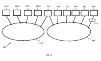
- FIG. 3a shows a schematic representation of a bus system 310 comprising two rings 312, 314.
- Each of the rings is provided by a multicore processor, e.g. a cell processor.
- the multicore processor comprising the bus system 312 contains the control element according to the invention.
- the two rings 312, 314 are connected via a FIFO buffer 320.
- the multicore processors comprising the respective rings 312, 314 can communicate directly with each other.
- the two rings 312, 314 are connected via a FPGA 320 and can communicate indirectly via this FPGA.
- the bus system 310 can be adapted to carry out the method according to the invention.
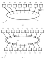
- FIG. 3b shows a schematic representation of a bus system 340 comprising four ring busses 312, 314, 352 and 354.
- the bus system 340 comprises the bus system 310, as shown in Fig. 3a .
- Each ring bus 312, 314, 352 and 354 constitutes a multicore processor, e.g. a cell processor.
- a plurality of different elements can be connected to the ring busses, as e.g. Inter-Integrated Circuits (I 2 C), Network interface controllers (NIC), Random-access memories (RAMs), Storages, buffers, as e.g. First In, First Out buffers (FIFO, etc..
- the elements of the ring busses e.g. the RAMs, storages, NICs I2C, etc.
- the bus system 340 comprises two sets, each comprising two multicore processors, i.e. the set of processors 312, 314 (as also shown in Fig. 3a ) and the set of processors 352, 354.
- the processors of one set are directly communicating with each other, as explained above, over respective FIFO buffers 312 and 362.
- the sets are connected to each other by (and preferably communicating via) a FPGA 361.
- each processor is connected by a respective XIO link 363, 364, 365 and 366 to the FPGA 361.
- the each link 363, 364, 365 and 366 may also comprise a plurality of XIO links, preferably in parallel.
- the interface between each of the processors and the respective XIO link 363, 364, 365 and 366 is provided by FIFO buffers of the processors.
- One of the processors e.g. the processor 312 can comprise the control element according to the invention.
- the two sets together i.e. the four processors 312, 314, 362, 364, can be adapted to carry out the method according to invention.
- each processing element i.e. processor core
- each processing element comprised by the four processors 312, 314, 362, 364 can be used in parallel.
- the bus system 340 preferably comprises still a third set (not shown), wherein the third set corresponds to the first and second set shown in Fig. 3b and explained above.
- the three sets together i.e. the six processors comprised by the three sets, can be adapted to carry out the method according to invention.
- four, five, six or even more sets can be connected together, wherein also each set can comprise more than two processors, in order to carry out together the method according to the invention.
- the FPGA 361 additionally comprises at least one transceiver and/or General Purpose Input/Output (GPIO) which can provide a network interface 367.
- the interface 367 can be a small form-factor pluggable (SFP) or an enhanced small form-factor pluggable (SFP+), e.g. a Quad Small Form-factor Pluggable (QSFP or QSFP+), or a plurality of unkeyed 8P8C modular connectors (e.g. RJ45).
- the interface 367 might also comprise a combination of enhanced small form-factor pluggable (SFP+) and unkeyed 8P8C modular connectors (e.g. RJ45).
- the FPGA can also be connected to at least one further FPGA (not shown) which comprises the network interface as described above.+
- FIG. 4 shows a schematic representation of a ring bus 412, wherein the pointer to the current active element is indicated as P0 and pointers to the next active elements are indicated as P1 to P7.
- a processing core 420 which acts as a control element, a RAM 422, a Flash 424, a storage 426, an NIC 428, an I2C bus 430, a PCIe 432 and other elements 434 are connected to the ring bus 412, wherein the other elements 434 are connected to the ring bus 412 via a FIFO buffer 435.
- the ring bus 412 is configured to transport data in a clock-wise direction and also the pointer passes through the ring in a clockwise direction.
- the elements are separated by the distance of one clock cycle.
- Other embodiments may provide that the pointer position passes through the ring with different time increments which may or may not be equal in length.
- the forwarding of the pointer can be decided e.g. based on static priorities that are assigned to the different elements.
- FIG. 5 shows a schematic representation of a further bus system 510 in accordance with the present invention.
- the method according to the present invention leads to a reduction of the cycle time to less than a third of the cycle time according to the prior art approach.
- the n connected elements correspond to n different pointer positions.
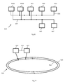
- FIG. 6 shows a schematic representation of a further bus system 610 in accordance with the present invention.
- the bus system 610 is set-up with two bi-directional busses 612, 614 with a linear topology and a time division multiple access scheme.
- Fig. 6 shows three elements 620, 622, 640 that are connected to both linear busses 612, 614.
- Several of these elements can act as control elements, with the other elements acting as processing elements, controlled by the control elements.
- other elements e.g. a RAM controller could be connected to the busses 612, 614, too.
- the bus system 610 can also be set up using a token passing scheme where the token is passed from one station to the next, wherein the "next" station is defined based on the addresses of the bus interfaces of the elements connected to the bus.
- the pointer can be pushed or pulled by a connected control element to receive or send data to or from any other connected element.
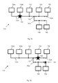
- Figure 7 shows a schematic representation of a non-exclusive bus system 710 that comprises three linear parts 712a, 712b, 712c that are connected through a branch 713.
- Connected to the bus system 710 are: two control elements 720a, 720b and a RAM 722 that are connected to the first linear part 712a, two processing elements 730, 732 that are connected to the second linear part 712b and two processing elements 740, 742 that are connected to the third linear part 712c of the bus system 710.
- second and third linear part 712b, 712c shown in Fig. 7 there can be any number of additional linear parts which are also connected to the first linear part 712a. These additional linear parts can comprise the same number of connected elements.
- the RAM component 722 has a total of three physical neighbours: control element 720b, processing element 730 of the second part 712b and processing element 740 of the third part 712c. Therefore, access to this bus system 710 should be managed with a token passing scheme where the neighbour relations are defined based on the addresses of the connected elements. It should be noted that linear parts 712b and 712c can be active at the same time. Temporary or second-level tokens are used to assign the active slot within one linear part. Knowledge about the current state and the predicted future availability of the linear parts can be used by the cycle prediction method and by the decision which processing elements the subtasks are assigned to.
- a primary branch part and a plurality of secondary branch parts there is a primary branch part and a plurality of secondary branch parts. This is illustrated in Figs. 7a and 7b , where the first linear part 712a forms a primary branch and second and third linear part 712b ,712c form a secondary branch part.
- the global token 750 is indicated in Figs. 7a and 7b as a big star, the local token 752 as a small star. If the global token 750 is present on the primary branch part, as shown in Fig. 7a , there cannot be any local tokens on any of the secondary branch parts. However if the global token 750 is present on one of the secondary branch parts, as shown in Fig. 7b , it is possible to allow for local tokens 752 in all or some of the other secondary branch parts which cannot leave their individual secondary branch parts.
- Figure 8 shows a schematic representation of a non-exclusive bus system 810 comprising two bi-directional busses 812, 814.
- a first control element 820a, a second control element 820b and a RAM 822 are connected to both the first bus 812 and the second bus 814.
- a number of n processing elements 830, 832 are connected only to the second bus 814 and a number of n processing elements 840, 842 are connected only to the first bus 812.
- This set-up can be repeated n times such that there is a total of m*n processing elements connected to the bus system.
- the set-up shown in Fig. 8 has the advantage that for example the communication between the control elements 820a, 820b and RAM 822 can occur both through the first bus 812 and the second bus 814.
- Access to the busses 812, 814 can be implemented with a simple time division multiple access scheme. Alternatively, for example a token passing scheme or a combination of the two can be used.
- bus systems shown in the drawings can comprise further elements and further busses that are not shown in the drawings.
- branches as shown in Fig. 7 could also connect ring busses with linear parts.
- different busses that are connected via a bridge or share at least one element could use different access schemes.
- Figure 9 shows a schematic representation of a non-exclusive bus system 910 comprising ring busses 912, 214 with a processing core 920 and a RAM 922 connected to them. Furthermore, the processing core 920 and the RAM 922 are connected through a direct connection 921. Further elements can be connected to the ring busses 912, 914, but are not shown in Fig. 9 .
- the ring busses shown in Figures 1 and 9 can also be implemented with access protocols where the active time slot is passed from a first element to the next element when the first element is finished with accessing the bus.
- This can be implement e.g. as a token ring access scheme, where an element passes the token to the next element when it has finished accessing the bus.
Priority Applications (8)
| Application Number | Priority Date | Filing Date | Title |
|---|---|---|---|
| EP15163717.0A EP3082038A1 (de) | 2015-04-15 | 2015-04-15 | Verfahren, vorrichtung und system zur erzeugung eines massiv parallelisierten, ausführbaren objekts |
| CN201680016138.8A CN107430525A (zh) | 2015-04-15 | 2016-04-04 | 用于创建大规模并行化可执行对象的方法、装置以及系统 |
| PCT/EP2016/057344 WO2016165969A1 (en) | 2015-04-15 | 2016-04-04 | Method, device and system for creating a massively parallelised executable object |
| KR1020177025698A KR20170137061A (ko) | 2015-04-15 | 2016-04-04 | 대규모 병렬 실행 가능 객체를 생성하는 방법, 디바이스 및 시스템 |
| CA2982975A CA2982975A1 (en) | 2015-04-15 | 2016-04-04 | Method, device and system for creating a massively parallelised executable object |
| TW105111650A TW201706838A (zh) | 2015-04-15 | 2016-04-14 | 用以建立大規模平行化可執行物件之方法、裝置及系統 |
| IL253506A IL253506A0 (en) | 2015-04-15 | 2017-07-16 | Method, device and system for optimizing machine code that is executed on a device that has one or more buses |
| US15/783,136 US20180095738A1 (en) | 2015-04-15 | 2017-10-13 | Method, device, and system for creating a massively parallilized executable object |
Applications Claiming Priority (1)
| Application Number | Priority Date | Filing Date | Title |
|---|---|---|---|
| EP15163717.0A EP3082038A1 (de) | 2015-04-15 | 2015-04-15 | Verfahren, vorrichtung und system zur erzeugung eines massiv parallelisierten, ausführbaren objekts |
Publications (1)
| Publication Number | Publication Date |
|---|---|
| EP3082038A1 true EP3082038A1 (de) | 2016-10-19 |
Family
ID=53039217
Family Applications (1)
| Application Number | Title | Priority Date | Filing Date |
|---|---|---|---|
| EP15163717.0A Withdrawn EP3082038A1 (de) | 2015-04-15 | 2015-04-15 | Verfahren, vorrichtung und system zur erzeugung eines massiv parallelisierten, ausführbaren objekts |
Country Status (8)
| Country | Link |
|---|---|
| US (1) | US20180095738A1 (de) |
| EP (1) | EP3082038A1 (de) |
| KR (1) | KR20170137061A (de) |
| CN (1) | CN107430525A (de) |
| CA (1) | CA2982975A1 (de) |
| IL (1) | IL253506A0 (de) |
| TW (1) | TW201706838A (de) |
| WO (1) | WO2016165969A1 (de) |
Cited By (1)
| Publication number | Priority date | Publication date | Assignee | Title |
|---|---|---|---|---|
| WO2019048222A1 (de) * | 2017-09-11 | 2019-03-14 | Siemens Mobility GmbH | Schienenfahrzeug mit mehrkernrechenleistung |
Families Citing this family (32)
| Publication number | Priority date | Publication date | Assignee | Title |
|---|---|---|---|---|
| US9146764B1 (en) | 2014-09-30 | 2015-09-29 | Amazon Technologies, Inc. | Processing event messages for user requests to execute program code |
| US9830193B1 (en) | 2014-09-30 | 2017-11-28 | Amazon Technologies, Inc. | Automatic management of low latency computational capacity |
| US9678773B1 (en) | 2014-09-30 | 2017-06-13 | Amazon Technologies, Inc. | Low latency computational capacity provisioning |
| US9600312B2 (en) | 2014-09-30 | 2017-03-21 | Amazon Technologies, Inc. | Threading as a service |
| US9537788B2 (en) | 2014-12-05 | 2017-01-03 | Amazon Technologies, Inc. | Automatic determination of resource sizing |
| US9733967B2 (en) | 2015-02-04 | 2017-08-15 | Amazon Technologies, Inc. | Security protocols for low latency execution of program code |
| US9588790B1 (en) | 2015-02-04 | 2017-03-07 | Amazon Technologies, Inc. | Stateful virtual compute system |
| US9910713B2 (en) | 2015-12-21 | 2018-03-06 | Amazon Technologies, Inc. | Code execution request routing |
| US11132213B1 (en) | 2016-03-30 | 2021-09-28 | Amazon Technologies, Inc. | Dependency-based process of pre-existing data sets at an on demand code execution environment |
| US10102040B2 (en) | 2016-06-29 | 2018-10-16 | Amazon Technologies, Inc | Adjusting variable limit on concurrent code executions |
| US10725826B1 (en) * | 2017-06-21 | 2020-07-28 | Amazon Technologies, Inc. | Serializing duration-limited task executions in an on demand code execution system |
| US10541939B2 (en) * | 2017-08-15 | 2020-01-21 | Google Llc | Systems and methods for provision of a guaranteed batch |
| US10853115B2 (en) | 2018-06-25 | 2020-12-01 | Amazon Technologies, Inc. | Execution of auxiliary functions in an on-demand network code execution system |
| US11146569B1 (en) | 2018-06-28 | 2021-10-12 | Amazon Technologies, Inc. | Escalation-resistant secure network services using request-scoped authentication information |
| US10949237B2 (en) | 2018-06-29 | 2021-03-16 | Amazon Technologies, Inc. | Operating system customization in an on-demand network code execution system |
| US11099870B1 (en) | 2018-07-25 | 2021-08-24 | Amazon Technologies, Inc. | Reducing execution times in an on-demand network code execution system using saved machine states |
| US11099917B2 (en) | 2018-09-27 | 2021-08-24 | Amazon Technologies, Inc. | Efficient state maintenance for execution environments in an on-demand code execution system |
| US11243953B2 (en) | 2018-09-27 | 2022-02-08 | Amazon Technologies, Inc. | Mapreduce implementation in an on-demand network code execution system and stream data processing system |
| TWI672649B (zh) * | 2018-09-27 | 2019-09-21 | 宏碁股份有限公司 | 執行例行工作的方法與電子裝置 |
| US11943093B1 (en) | 2018-11-20 | 2024-03-26 | Amazon Technologies, Inc. | Network connection recovery after virtual machine transition in an on-demand network code execution system |
| US11010188B1 (en) | 2019-02-05 | 2021-05-18 | Amazon Technologies, Inc. | Simulated data object storage using on-demand computation of data objects |
| US11861386B1 (en) | 2019-03-22 | 2024-01-02 | Amazon Technologies, Inc. | Application gateways in an on-demand network code execution system |
| US11119809B1 (en) | 2019-06-20 | 2021-09-14 | Amazon Technologies, Inc. | Virtualization-based transaction handling in an on-demand network code execution system |
| US11115404B2 (en) | 2019-06-28 | 2021-09-07 | Amazon Technologies, Inc. | Facilitating service connections in serverless code executions |
| US11159528B2 (en) | 2019-06-28 | 2021-10-26 | Amazon Technologies, Inc. | Authentication to network-services using hosted authentication information |
| US11190609B2 (en) | 2019-06-28 | 2021-11-30 | Amazon Technologies, Inc. | Connection pooling for scalable network services |
| US11119826B2 (en) | 2019-11-27 | 2021-09-14 | Amazon Technologies, Inc. | Serverless call distribution to implement spillover while avoiding cold starts |
| US11714682B1 (en) | 2020-03-03 | 2023-08-01 | Amazon Technologies, Inc. | Reclaiming computing resources in an on-demand code execution system |
| US11188391B1 (en) | 2020-03-11 | 2021-11-30 | Amazon Technologies, Inc. | Allocating resources to on-demand code executions under scarcity conditions |
| US11593270B1 (en) | 2020-11-25 | 2023-02-28 | Amazon Technologies, Inc. | Fast distributed caching using erasure coded object parts |
| US11550713B1 (en) | 2020-11-25 | 2023-01-10 | Amazon Technologies, Inc. | Garbage collection in distributed systems using life cycled storage roots |
| US11388210B1 (en) | 2021-06-30 | 2022-07-12 | Amazon Technologies, Inc. | Streaming analytics using a serverless compute system |
Citations (1)
| Publication number | Priority date | Publication date | Assignee | Title |
|---|---|---|---|---|
| EP2466460A1 (de) * | 2010-12-17 | 2012-06-20 | Samsung Electronics Co., Ltd | Vorrichtung und Verfahren zum Compilieren für eine Vorrichtung mit Mehrfachkern |
Family Cites Families (10)
| Publication number | Priority date | Publication date | Assignee | Title |
|---|---|---|---|---|
| US4748585A (en) * | 1985-12-26 | 1988-05-31 | Chiarulli Donald M | Processor utilizing reconfigurable process segments to accomodate data word length |
| WO2004001584A2 (en) * | 2002-06-24 | 2003-12-31 | Ante Vista Gmbh | A method for executing structured symbolic machine code on a microprocessor |
| JP3938387B2 (ja) * | 2005-08-10 | 2007-06-27 | インターナショナル・ビジネス・マシーンズ・コーポレーション | コンパイラ、制御方法、およびコンパイラ・プログラム |
| US7757040B2 (en) * | 2007-01-30 | 2010-07-13 | International Business Machines Corporation | Memory command and address conversion between an XDR interface and a double data rate interface |
| US9658840B2 (en) * | 2007-05-22 | 2017-05-23 | Philips Lighting Holding B.V. | Compiler and compiling method for a networked control system comprising a plurality of devices |
| JP4629768B2 (ja) * | 2008-12-03 | 2011-02-09 | インターナショナル・ビジネス・マシーンズ・コーポレーション | 並列化処理方法、システム、及びプログラム |
| US8707314B2 (en) * | 2011-12-16 | 2014-04-22 | Advanced Micro Devices, Inc. | Scheduling compute kernel workgroups to heterogeneous processors based on historical processor execution times and utilizations |
| US20140189330A1 (en) * | 2012-12-27 | 2014-07-03 | Ayal Zaks | Optional branches |
| US20140208297A1 (en) * | 2013-01-20 | 2014-07-24 | International Business Machines Corporation | Validation of revised computer programs |
| US9348560B2 (en) * | 2013-06-04 | 2016-05-24 | Qualcomm Incorporated | Efficient execution of graph-based programs |
-
2015
- 2015-04-15 EP EP15163717.0A patent/EP3082038A1/de not_active Withdrawn
-
2016
- 2016-04-04 WO PCT/EP2016/057344 patent/WO2016165969A1/en active Application Filing
- 2016-04-04 CN CN201680016138.8A patent/CN107430525A/zh active Pending
- 2016-04-04 KR KR1020177025698A patent/KR20170137061A/ko unknown
- 2016-04-04 CA CA2982975A patent/CA2982975A1/en not_active Abandoned
- 2016-04-14 TW TW105111650A patent/TW201706838A/zh unknown
-
2017
- 2017-07-16 IL IL253506A patent/IL253506A0/en unknown
- 2017-10-13 US US15/783,136 patent/US20180095738A1/en not_active Abandoned
Patent Citations (1)
| Publication number | Priority date | Publication date | Assignee | Title |
|---|---|---|---|---|
| EP2466460A1 (de) * | 2010-12-17 | 2012-06-20 | Samsung Electronics Co., Ltd | Vorrichtung und Verfahren zum Compilieren für eine Vorrichtung mit Mehrfachkern |
Non-Patent Citations (2)
| Title |
|---|
| NYSTROM E ET AL: "Effective cluster assignment for modulo scheduling", MICRO-31. PROCEEDINGS OF THE 31ST. ANNUAL ACM/IEEE INTERNATIONAL SYMPOSIUM ON MICROARCHITECTURE. DALLAS, TX, NOV. 30 - DEC. 2, 1998; [PROCEEDINGS OF THE ANNUAL ACM/IEEE INTERNATIONAL SYMPOSIUM ON MICROARCHITECTURE], LOS ALMITOS, CA : IEEE COMP. SOC,, 30 November 1998 (1998-11-30), pages 103 - 114, XP010318242, ISBN: 978-0-8186-8609-2, DOI: 10.1109/MICRO.1998.742773 * |
| ORLANDO S ET AL: "A TEMPLATE FOR NON-UNIFORM PARALLEL LOOPS BASED ON DYNAMIC SCHEDULING AND PREFETCHING TECHNIQUES", PROCEEDINGS OF THE 1996 INTERNATIONAL CONFERENCE ON SUPERCOMPUTING. PHILADELPHIA, MAY 25 - 28, 1996; [PROCEEDINGS OF THE INTERNATIONAL CONFERENCE ON SUPERCOMPUTING], NEW YORK, ACM, US, vol. CONF. 10, 25 May 1996 (1996-05-25), pages 117 - 124, XP000683014, ISBN: 978-0-89791-803-9, DOI: 10.1145/237578.237593 * |
Cited By (1)
| Publication number | Priority date | Publication date | Assignee | Title |
|---|---|---|---|---|
| WO2019048222A1 (de) * | 2017-09-11 | 2019-03-14 | Siemens Mobility GmbH | Schienenfahrzeug mit mehrkernrechenleistung |
Also Published As
| Publication number | Publication date |
|---|---|
| CN107430525A (zh) | 2017-12-01 |
| US20180095738A1 (en) | 2018-04-05 |
| IL253506A0 (en) | 2017-09-28 |
| KR20170137061A (ko) | 2017-12-12 |
| TW201706838A (zh) | 2017-02-16 |
| WO2016165969A1 (en) | 2016-10-20 |
| CA2982975A1 (en) | 2016-10-20 |
Similar Documents
| Publication | Publication Date | Title |
|---|---|---|
| US20180095738A1 (en) | Method, device, and system for creating a massively parallilized executable object | |
| US8572586B2 (en) | Optimized scalar promotion with load and splat SIMD instructions | |
| CN109697185B (zh) | 多瓦片处理阵列中的同步 | |
| JP5736034B2 (ja) | 階層型分散処理システムのためのソフトウェアのコンパイル | |
| US11237880B1 (en) | Dataflow all-reduce for reconfigurable processor systems | |
| US8671418B2 (en) | Environment modification in a hybrid node computing environment | |
| US11392740B2 (en) | Dataflow function offload to reconfigurable processors | |
| US20130218299A1 (en) | MCP Scheduling For Parallelization Of LAD/FBD Control Program In Multi-Core PLC | |
| CA2433379A1 (en) | Modulo scheduling of multiple instruction chains | |
| Kaushik et al. | Computation and communication aware run-time mapping for NoC-based MPSoC platforms | |
| EP2759927B1 (de) | Vorrichtung und Verfahren zur gemeinsamen Nutzung der Funktionslogik zwischen Funktionseinheiten und rekonfigurierbarer Prozessor dafür | |
| KR20150121108A (ko) | 실행가능 코드를 실행하기 위한 방법, 처리 모듈 및 시스템 | |
| EP2998864B1 (de) | Verfahren, Vorrichtung und System zur Festlegung eines Verteilungswegs einer Aufgabe | |
| EP3495960A1 (de) | Programm, vorrichtung und verfahren zur kommunikation von daten zwischen parallelen prozessorkernen | |
| WO2011114539A1 (en) | A programming supporting device and a method for generating routing information for an array of computing nodes | |
| US20240020265A1 (en) | Operating a Cost Estimation Tool for Placing and Routing an Operation Unit Graph on a Reconfigurable Processor | |
| WO2022166480A1 (zh) | 任务调度方法、装置及系统 | |
| WO2021056277A1 (zh) | 一种执行程序的方法 | |
| Samman et al. | Architecture, on-chip network and programming interface concept for multiprocessor system-on-chip | |
| CN115543448A (zh) | 数据流架构上的指令动态调度方法、数据流架构 | |
| JP2008276321A (ja) | 情報処理システムおよび情報処理方法 | |
| JP2013174934A (ja) | 計算機システム |
Legal Events
| Date | Code | Title | Description |
|---|---|---|---|
| PUAI | Public reference made under article 153(3) epc to a published international application that has entered the european phase |
Free format text: ORIGINAL CODE: 0009012 |
|
| AK | Designated contracting states |
Kind code of ref document: A1 Designated state(s): AL AT BE BG CH CY CZ DE DK EE ES FI FR GB GR HR HU IE IS IT LI LT LU LV MC MK MT NL NO PL PT RO RS SE SI SK SM TR |
|
| AX | Request for extension of the european patent |
Extension state: BA ME |
|
| RIN1 | Information on inventor provided before grant (corrected) |
Inventor name: ASLAN, HALIS Inventor name: SAREMI, FARBOD Inventor name: ZIELINSKI, TOBIAS Inventor name: DUERKOP, HENDRIK |
|
| RAP1 | Party data changed (applicant data changed or rights of an application transferred) |
Owner name: HYBRIDSERVER TEC GMBH |
|
| 17P | Request for examination filed |
Effective date: 20170302 |
|
| RBV | Designated contracting states (corrected) |
Designated state(s): AL AT BE BG CH CY CZ DE DK EE ES FI FR GB GR HR HU IE IS IT LI LT LU LV MC MK MT NL NO PL PT RO RS SE SI SK SM TR |
|
| RAP1 | Party data changed (applicant data changed or rights of an application transferred) |
Owner name: HYBRIDSERVER TEC IP GMBH |
|
| 17Q | First examination report despatched |
Effective date: 20170518 |
|
| REG | Reference to a national code |
Ref country code: HK Ref legal event code: DE Ref document number: 1230301 Country of ref document: HK |
|
| STAA | Information on the status of an ep patent application or granted ep patent |
Free format text: STATUS: THE APPLICATION IS DEEMED TO BE WITHDRAWN |
|
| 18D | Application deemed to be withdrawn |
Effective date: 20171130 |
|
| REG | Reference to a national code |
Ref country code: HK Ref legal event code: WD Ref document number: 1230301 Country of ref document: HK |