EP3078188B1 - Variable gain column amplifier adapted for use in imaging arrays - Google Patents
Variable gain column amplifier adapted for use in imaging arrays Download PDFInfo
- Publication number
- EP3078188B1 EP3078188B1 EP14868356.8A EP14868356A EP3078188B1 EP 3078188 B1 EP3078188 B1 EP 3078188B1 EP 14868356 A EP14868356 A EP 14868356A EP 3078188 B1 EP3078188 B1 EP 3078188B1
- Authority
- EP
- European Patent Office
- Prior art keywords
- signal
- gain
- voltage
- voltage signal
- pixel
- Prior art date
- Legal status (The legal status is an assumption and is not a legal conclusion. Google has not performed a legal analysis and makes no representation as to the accuracy of the status listed.)
- Active
Links
Images



Classifications
-
- H—ELECTRICITY
- H04—ELECTRIC COMMUNICATION TECHNIQUE
- H04N—PICTORIAL COMMUNICATION, e.g. TELEVISION
- H04N23/00—Cameras or camera modules comprising electronic image sensors; Control thereof
- H04N23/95—Computational photography systems, e.g. light-field imaging systems
- H04N23/951—Computational photography systems, e.g. light-field imaging systems by using two or more images to influence resolution, frame rate or aspect ratio
-
- H—ELECTRICITY
- H04—ELECTRIC COMMUNICATION TECHNIQUE
- H04N—PICTORIAL COMMUNICATION, e.g. TELEVISION
- H04N25/00—Circuitry of solid-state image sensors [SSIS]; Control thereof
- H04N25/60—Noise processing, e.g. detecting, correcting, reducing or removing noise
- H04N25/616—Noise processing, e.g. detecting, correcting, reducing or removing noise involving a correlated sampling function, e.g. correlated double sampling [CDS] or triple sampling
-
- H—ELECTRICITY
- H04—ELECTRIC COMMUNICATION TECHNIQUE
- H04N—PICTORIAL COMMUNICATION, e.g. TELEVISION
- H04N25/00—Circuitry of solid-state image sensors [SSIS]; Control thereof
- H04N25/70—SSIS architectures; Circuits associated therewith
- H04N25/76—Addressed sensors, e.g. MOS or CMOS sensors
- H04N25/78—Readout circuits for addressed sensors, e.g. output amplifiers or A/D converters
Definitions
- Imaging arrays fabricated in CMOS are utilized in numerous cameras. In digital photography, the image is recorded by an imaging array in which each pixel includes a photodetector that measures the amount of light that falls on some portion of the pixel area. Imaging arrays that have a high dynamic range are required for many applications, including scientific research photography. The dynamic range of an imaging array will be defined to be the ratio of the maximum signal for a pixel to the minimum signal that is above the noise.
- the imaging arrays are constructed from a two-dimensional array of pixel sensors organized as a plurality of rows and columns of pixel sensors. All of the pixel sensors in a given column are connected to a common signal line. The specific pixel in a column that is currently being readout is determined by a row select signal that connects all of the pixel sensors in a given row to their respective signal lines.
- each signal line has a dedicated signal amplifier and readout circuit so that the entire row of pixel sensors can be readout in parallel.
- the readout amplifier and associated analog-to-digital converters (ADCs) must have a dynamic range that is commensurate with the dynamic range of the individual pixels and must provide a readout time for each pixel that is as short as possible, particularly in low light images, as the noise in each pixel value increases with the time between the end of an exposure and the time the pixel is readout.
- ADCs analog-to-digital converters
- schemes in which multiple readout amplifiers are used on each signal line have been proposed. For example, US Patent Application 12/036,998 filed 2/25/2008 describes a readout system in which digitization circuits having different gains are implemented for each readout line, the choice of digitization gain being determined by the signal on the readout line in question.
- US2004/080637A1 discloses that an image sensor controls the gain of a pixel signal on a pixel-by-pixel basis and extends a dynamic range while maintaining a S/N ratio at a favorable level.
- a column unit in an image sensor independently detects a level of each pixel signal and independently sets a gain for level of the signal.
- a photoelectric converting region unit has pixels arranged two-dimensionally with a vertical signal line for each pixel column to output each pixel signal. The column unit is on an output side of the vertical signal line.
- the column unit for each pixel column has a pixel signal level detecting circuit, a programmable gain control, a sample and hold (S/H) circuit. Gain correction is performed according to a result of a detected level of the pixel signal.
- EP1223549A1 discloses an analog-to-digital converter array which includes one analog-to-digital converter for each row of photodetectors in the photodetector array.
- the image-processing unit includes the plurality of processing circuits for performing high-speed image processing.
- the signal converter combines the output signals from the analog-to-digital converter array with output signals from the image-processing unit Under control of the control circuit and the signal conversion controller, the signal converter downconverts the composite signal at an important timing to a frame rate suitable for display on the monitor and subsequently displays the signal on the monitor.
- CMOS Front-End for CCD Cameras discloses a system in which all the functions previously residing on a bipolar chip have been incorporated on the same CMOS die with the ADC, including a CDS block, an amplifier with variable gain from 0 to 34dB, a black-level correction loop, an input clamp and a voltage reference.
- An emitter follower buffer is traditionally used between the CCD and the rest of the system for line driving, but this is the only portion of the analog signal chain external to the chip.
- US 2011/134295 discloses an image sensor comprising a pixel array, column A/D converters and a circuit in which a signal from the same pixel is read from a column amplifier twice with different amplification factors, and each of the read signals are then subjected to A/D conversion in a column A/D converter before selection of the signals takes place.
- a noise reduction step is performed twice, once for each of the two differently amplified signals wherein the gain applied during the reset and pixel signal reading is the same.
- the present invention as set out in independent claims includes an imaging sensor using a novel bit line processing circuit, that processing circuit, and the method of processing the pixel outputs from an image sensor using that processing circuit.
- the image sensor includes an array of pixel sensors, a signal digitizing circuit, and a digitizing controller.
- Each pixel sensor in the array of pixel sensors includes a photodetector, a charge conversion circuit, and a gate transistor, the charge conversion circuit generating a voltage signal that is a function of a charge on the photodetector, and the gate transistor coupling the voltage signal to a bit line in response to a first signal.
- the signal digitizing circuit is connected to the bit line, the digitizing circuit converting the voltage signal to a plurality of output digital values, said output digital values having selectable levels of digitization noise, one of the levels of digitization noise being selected in response to an output selection signal used with each signal value.
- the digitizing controller generates the output control signal based on the voltage signal.
- the signal digitizing circuit includes a variable gain amplifier having a plurality of gain values that amplifies the voltage signal to generate an amplified signal that is digitized by an ADC having a fixed number of bits.
- the variable gain amplifier includes a capacitive transimpedance amplifier having a feedback capacitance that is determined by the output control signal.
- Imaging array 20 is constructed from a rectangular array of pixel sensors 21.
- Each pixel sensor includes a photodiode 26 and an interface circuit 27.
- the details of the interface circuit depend on the particular pixel design. However, all of the pixel circuits include a gate that is connected to a row line 22 that is used to connect that pixel to a bit line 23. The specific row that is enabled at any time is determined by a bit address that is input to a row decoder 25.
- the various bit lines terminate in a column processing circuit 28 that typically includes sense amplifiers and ADCs. Each sense amplifier reads the signal produced by the pixel that is currently connected to the bit line processed by that sense amplifier. At any given time, a single pixel sensor is readout. The specific column that is readout is determined by a column address that is utilized by a column decoder 24 to connect the ADC output from that column to circuitry that is external to the imaging array. The overall operation of the imaging array is controlled by a controller 29 that receives the row and column addresses and other commands on an input bus.
- Pixel sensor 31 includes a photodiode 38, which is preferably a pinned photodiode, that is coupled to a floating diffusion node 39 by gate 32.
- photodiode 38 which is preferably a pinned photodiode
- charge accumulates in photodiode 38.
- the accumulated charge is transferred to floating diffusion node 39 by applying a signal to gate 32.
- the charge transferred to floating diffusion node 39 is converted to voltage by the parasitic capacitor 30 associated with the gate of transistor 34, which is connected as a source follower.
- Transistor 34 provides the gain needed to drive bit line 37 when pixel sensor 31 is connected to that bit line via a signal on row select line 36 that is coupled to the gate of transistor 35.
- the potential on floating diffusion node 39 Prior to transferring charge from photodiode 38 to floating diffusion node 39, the potential on floating diffusion node 39 is reset to a predetermined potential via gate 33.
- the voltage on floating diffusion node 39 is reduced by an amount that depends on the charge that was transferred and the capacitance of the floating diffusion node. However, there are small variations in the final voltage on floating diffusion node 39 after the reset.
- a procedure known as correlated double sampling is used to compensate for these variations.
- the potential on floating diffusion node 39 after floating diffusion node 39 has been reset is measured by connecting pixel sensor 31 to bit line 37. After this starting potential is measured, the charge that accumulated on photodiode 38 is transferred to floating diffusion node 39 and the potential on floating diffusion node 39 is again measured by connecting pixel sensor 31 to bit line 37. The difference in the signal between the two potential measurements determines the light intensity value that is reported for pixel sensor 31.
- the digitization gain is a function of the signal strength from the pixel.
- the first is the sensor noise of the photodiode and the analog readout circuitry, and the second results from the finite steps of the ADC used to convert the analog measurements to the final digital values for the pixels.
- the sensor noise is the sum of the shot noise from the photodetector, and thermal and 1/f noise from the readout electronics. Shot noise typically dominates the sensor noise for signal levels above ten photons.
- the output of the ADC has an uncertainty of one half the voltage difference corresponding to the least significant bit of the digital value. This uncertainty will be referred to as the "quantization noise" in the following discussion.
- CMOS imaging technology has resulted in image sensors with extremely low sensor noise levels, corresponding to the signal that would be produced from receiving as few as two photons.
- a digitization circuit having low quantization noise and high gain should be utilized. If such a digitization circuit is used to convert signals from pixels having high light intensities, however, the output voltages will be too high for conventional low cost CMOS circuitry to process.
- the ADCs would need to have a large number of bits, which further increases the cost and area of silicon required.
- the amplifier gain in the digitization circuit is set to a low value to maintain the signal within the range of CMOS circuitry when the analog signals from high intensity pixels are processed, the quantization noise will mask the low level signals.
- schemes in which ADCs that provide a variable quantization noise have been proposed.
- the prior art schemes discussed above utilize two ADCs having differing conversion gains with the gains being switched in response to the signal level from the pixel being processed so that low level signals are processed with smaller step sizes in the ADCs.
- the present invention is based on the observation that a column processing circuit that provides different levels of quantization noise can be constructed from a single capacitive transimpedance amplifier with variable gain and a fixed step size ADC. Increasing the gain of the capacitive transimpedance amplifier when low light level pixels are being processed is equivalent to decreasing the step size in the ADC, and hence, reducing the digitization noise level.
- Figure 3 is a schematic drawing of a column processing circuit according to one embodiment of the present invention.
- Column processing circuit 70 amplifies and processes the signals on bit line 37.
- Capacitive transimpedance amplifier 50 is constructed from an operational amplifier 51 and two feedback capacitors shown at 52 and 53 having capacitances C 52 and C 53 , respectively.
- switch 54 is controlled by the output of a latching comparator shown at 68 and by controller 29 shown in Figure 1 .
- latching comparator 68 Prior to each voltage measurement on bit line 37, latching comparator 68 is reset and switch 55 is closed to short the input and output of operational amplifier 51. Initially, switch 54 is open, and operational amplifier 51 has its maximum gain. When a signal is transferred to capacitor 56 for measurement, the output of operational amplifier 51 rises. If the output of operational amplifier 51 exceeds V 2 , latching comparator 68 is set thereby generating a signal on line 67 which is used to close switch 54. The gain of capacitive transimpedance amplifier 50 is thus reduced to the low value.
- the output voltage is stored on either capacitor 63 or capacitor 64 in double sampling circuit 60 depending on the state of switches 61 and 62, respectively.
- the difference in potential is digitized by ADC 65 and the value output on line 66 together with a value indicative of the gain value of capacitive transimpedance amplifier 50 on line 67.
- capacitive transimpedance amplifier 50 and the associated correlated double sampling circuitry behave as a conventional column processing circuit in that the gain of capacitive transimpedance amplifier 50 is at the high value for both the reset and measurement phases of the correlated double sampling.
- the gain used to measure the reset potential will be different than the gain used to measure the charge that was transferred from the photodiode.
- the difference computation will be in error. In many cases, this does not cause a significant problem, because the correlated double sampling computation only provides a significant difference from the value that would be obtained by just measuring the charge that was stored in the photodiode in cases where the photodiode charge is small.
- a modified double sampling circuit in which the observed reset value is divided by an appropriate factor that depends on the difference in gain of the two phases can be utilized. Such a circuit will be discussed in more detail below.
- Capacitive transimpedance amplifier 50 can be viewed as a capacitive transimpedance amplifier with a variable capacitive feedback circuit as the feedback loop.
- the feedback capacitance is set to maintain the output signal below a predetermined signal level.
- Embodiments in which more than two capacitance levels are utilized can also be constructed to further increase the dynamic range of the capacitive transimpedance amplifier.
- Figure 4 illustrates a column processing circuit having a capacitive transimpedance amplifier with three gain levels.
- Column processing circuit 90 includes a capacitive transimpedance amplifier 79 having three feedback capacitors shown at 71-73. Feedback capacitors 72 and 73 are switched into the feedback loop by switches 74 and 75, respectively, in response to the output of operational amplifier 51 exceeding V 2 and V 3 , respectively.
- the signals on output lines 77 and 78 are readout together with the output of ADC 65.
- a first voltage representing the reset voltage is stored in the double sampling circuit prior to the column processing circuit determining the final gain of the capacitive transimpedance amplifier. If the gain is subsequently reduced to a lower gain in response to a high signal being detected, the reset voltage will be too high by a factor of the ratio of the gains in the high gain state and the state in which the reset voltage was stored.
- Figure 5 illustrates one embodiment of a double sampling circuit that can be used with the present invention to correct for a switch in gain of the column processing circuit.
- Double sampling circuit 80 assumes that the gain in the column processing circuit is limited to two values, a high gain, G H that is used during the measurement of the reset voltage in the pixel currently connected to the bit line, and at the beginning of the measurement of the light signal, and a low gain, G L , that used if the signal in the high gain mode is greater than a predetermined threshold during the measurement of the light signal.
- the processing of the pixel is divided into two phases, a reset phase and a light measurement phase.
- switches 81 and 82 are closed.
- the signal from the pixel is stored on capacitor 84 during this phase using gain G H .
- An identical signal is stored on capacitor 83.
- switch 82 is open, and the potential on capacitor 84 is the measured reset potential.
- the signal on capacitor 83 at the end of the light measurement phase wilt depend on the gain of the capacitive transimpedance amplifier at the end of the light measurement phase. If the gain remained at G H , the switch 87 remains open. In this case ADC 65 outputs the difference in the two input signals as measured with the G H gain.
- switch 87 is closed. Since switch 82 is open, the voltage on line 88 will be reduced by a factor that depends on the capacitance of capacitor 85.
- the capacitance of capacitor 85 is chosen such that the voltage on line 88 is multiplied by a factor of G L /G H , hence correcting for the different gains in the reset and light measurement phases.
- a double sampling circuit analogous to that shown in Figure 5 can also be constructed.
- capacitor 85 can be replaced by a variable capacitance having a value that depends on the highest gain used during the light measurement phase.
- the combination of switch 87 and capacitor 85 is a variable capacitance that has two values, 0 and a capacitance that provides the desired division of the stored voltage.
- the double sampling circuits described above utilize a variable capacitance to divide the measured reset voltage by the desired factor, other forms of a voltage divider could be utilized. The advantage of the capacitive system lies in its simplicity.
- each column of pixels is processed by a column processing circuit.
- the present invention can be utilized with any arrangement of pixels in which a plurality of pixels that are exposed to significantly different illumination levels share the same signal digitizing circuit via a common input line.
- other forms of photodetectors could be utilized in the pixels.
Landscapes
- Engineering & Computer Science (AREA)
- Multimedia (AREA)
- Signal Processing (AREA)
- Computing Systems (AREA)
- Theoretical Computer Science (AREA)
- Transforming Light Signals Into Electric Signals (AREA)
- Analogue/Digital Conversion (AREA)
Description
- Low cost imaging arrays fabricated in CMOS are utilized in numerous cameras. In digital photography, the image is recorded by an imaging array in which each pixel includes a photodetector that measures the amount of light that falls on some portion of the pixel area. Imaging arrays that have a high dynamic range are required for many applications, including scientific research photography. The dynamic range of an imaging array will be defined to be the ratio of the maximum signal for a pixel to the minimum signal that is above the noise.
- Typically, the imaging arrays are constructed from a two-dimensional array of pixel sensors organized as a plurality of rows and columns of pixel sensors. All of the pixel sensors in a given column are connected to a common signal line. The specific pixel in a column that is currently being readout is determined by a row select signal that connects all of the pixel sensors in a given row to their respective signal lines.
- To improve the readout time of the array, each signal line has a dedicated signal amplifier and readout circuit so that the entire row of pixel sensors can be readout in parallel. The readout amplifier and associated analog-to-digital converters (ADCs) must have a dynamic range that is commensurate with the dynamic range of the individual pixels and must provide a readout time for each pixel that is as short as possible, particularly in low light images, as the noise in each pixel value increases with the time between the end of an exposure and the time the pixel is readout. To increase the dynamic range of the readout circuit, schemes in which multiple readout amplifiers are used on each signal line have been proposed. For example,
US Patent Application 12/036,998 filed 2/25/2008 - While multiple readout digitization circuits can provide improved dynamic range, the improvement comes with a significant cost, since the number of transistors that must be included in the processing circuitry for each signal line is substantially increased. Since there can be thousands of columns of pixels, hence, signal lines, each additional transistor represents a significant increase in the area of silicon required to implement the readout array, and hence, the cost of the- image sensor.
-
US2004/080637A1 discloses that an image sensor controls the gain of a pixel signal on a pixel-by-pixel basis and extends a dynamic range while maintaining a S/N ratio at a favorable level. A column unit in an image sensor independently detects a level of each pixel signal and independently sets a gain for level of the signal. A photoelectric converting region unit has pixels arranged two-dimensionally with a vertical signal line for each pixel column to output each pixel signal. The column unit is on an output side of the vertical signal line. The column unit for each pixel column has a pixel signal level detecting circuit, a programmable gain control, a sample and hold (S/H) circuit. Gain correction is performed according to a result of a detected level of the pixel signal. -
EP1223549A1 discloses an analog-to-digital converter array which includes one analog-to-digital converter for each row of photodetectors in the photodetector array. The image-processing unit includes the plurality of processing circuits for performing high-speed image processing. The signal converter combines the output signals from the analog-to-digital converter array with output signals from the image-processing unit Under control of the control circuit and the signal conversion controller, the signal converter downconverts the composite signal at an important timing to a frame rate suitable for display on the monitor and subsequently displays the signal on the monitor. - Mangelsdorf C Et Al: "A CMOS Front-End for CCD Cameras" discloses a system in which all the functions previously residing on a bipolar chip have been incorporated on the same CMOS die with the ADC, including a CDS block, an amplifier with variable gain from 0 to 34dB, a black-level correction loop, an input clamp and a voltage reference. An emitter follower buffer is traditionally used between the CCD and the rest of the system for line driving, but this is the only portion of the analog signal chain external to the chip.
-
US 2011/134295 discloses an image sensor comprising a pixel array, column A/D converters and a circuit in which a signal from the same pixel is read from a column amplifier twice with different amplification factors, and each of the read signals are then subjected to A/D conversion in a column A/D converter before selection of the signals takes place. Thus, a noise reduction step is performed twice, once for each of the two differently amplified signals wherein the gain applied during the reset and pixel signal reading is the same. - The present invention as set out in independent claims includes an imaging sensor using a novel bit line processing circuit, that processing circuit, and the method of processing the pixel outputs from an image sensor using that processing circuit. The image sensor includes an array of pixel sensors, a signal digitizing circuit, and a digitizing controller. Each pixel sensor in the array of pixel sensors includes a photodetector, a charge conversion circuit, and a gate transistor, the charge conversion circuit generating a voltage signal that is a function of a charge on the photodetector, and the gate transistor coupling the voltage signal to a bit line in response to a first signal.
The signal digitizing circuit is connected to the bit line, the digitizing circuit converting the voltage signal to a plurality of output digital values, said output digital values having selectable levels of digitization noise, one of the levels of digitization noise being selected in response to an output selection signal used with each signal value. The digitizing controller generates the output control signal based on the voltage signal. The signal digitizing circuit includes a variable gain amplifier having a plurality of gain values that amplifies the voltage signal to generate an amplified signal that is digitized by an ADC having a fixed number of bits. In one aspect of the invention, the variable gain amplifier includes a capacitive transimpedance amplifier having a feedback capacitance that is determined by the output control signal. -
-
Figure 1 illustrates a block diagram of one embodiment of a CMOS imaging array according to the present invention. -
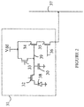
Figure 2 illustrates a schematic drawing of an exemplary pixel sensor that can be utilized in an imaging array. -
Figure 3 illustrates a schematic drawing of a column processing circuit according to one embodiment of the present invention. -
Figure 4 illustrates a column processing circuit having a capacitive transimpedance amplifier with three gain levels. -
Figure 5 illustrates one embodiment of a double sampling circuit that can be used with the present invention to correct for a switch in gain of the column processing circuit. - The manner in which the present invention provides its advantages can be more easily understood with reference to
Figure 1 , which is a block diagram of one embodiment of a CMOS imaging array according to the present invention.Imaging array 20 is constructed from a rectangular array ofpixel sensors 21. Each pixel sensor includes aphotodiode 26 and aninterface circuit 27. The details of the interface circuit depend on the particular pixel design. However, all of the pixel circuits include a gate that is connected to arow line 22 that is used to connect that pixel to abit line 23. The specific row that is enabled at any time is determined by a bit address that is input to arow decoder 25. - The various bit lines terminate in a
column processing circuit 28 that typically includes sense amplifiers and ADCs. Each sense amplifier reads the signal produced by the pixel that is currently connected to the bit line processed by that sense amplifier. At any given time, a single pixel sensor is readout. The specific column that is readout is determined by a column address that is utilized by acolumn decoder 24 to connect the ADC output from that column to circuitry that is external to the imaging array. The overall operation of the imaging array is controlled by acontroller 29 that receives the row and column addresses and other commands on an input bus. - Refer now to
Figure 2 , which is a schematic drawing of an exemplary pixel sensor that can be utilized inimaging array 20.Pixel sensor 31 includes aphotodiode 38, which is preferably a pinned photodiode, that is coupled to afloating diffusion node 39 bygate 32. During the exposure of the imaging array to the image being recorded, charge accumulates inphotodiode 38. The accumulated charge is transferred to floatingdiffusion node 39 by applying a signal togate 32. The charge transferred to floatingdiffusion node 39 is converted to voltage by theparasitic capacitor 30 associated with the gate oftransistor 34, which is connected as a source follower.Transistor 34 provides the gain needed to drivebit line 37 whenpixel sensor 31 is connected to that bit line via a signal on rowselect line 36 that is coupled to the gate oftransistor 35. Prior to transferring charge fromphotodiode 38 to floatingdiffusion node 39, the potential onfloating diffusion node 39 is reset to a predetermined potential viagate 33. When charge is transferred fromphotodiode 38 to the reset floatingdiffusion node 39, the voltage on floatingdiffusion node 39 is reduced by an amount that depends on the charge that was transferred and the capacitance of the floating diffusion node. However, there are small variations in the final voltage onfloating diffusion node 39 after the reset. - A procedure known as correlated double sampling is used to compensate for these variations. The potential on
floating diffusion node 39 after floatingdiffusion node 39 has been reset is measured by connectingpixel sensor 31 tobit line 37. After this starting potential is measured, the charge that accumulated onphotodiode 38 is transferred to floatingdiffusion node 39 and the potential on floatingdiffusion node 39 is again measured by connectingpixel sensor 31 tobit line 37. The difference in the signal between the two potential measurements determines the light intensity value that is reported forpixel sensor 31. - As noted above, it is advantageous to provide a digitization circuit for each bit line in which the digitization gain is a function of the signal strength from the pixel. In general, there are two sources of noise in each pixel measurement. The first is the sensor noise of the photodiode and the analog readout circuitry, and the second results from the finite steps of the ADC used to convert the analog measurements to the final digital values for the pixels. The sensor noise is the sum of the shot noise from the photodetector, and thermal and 1/f noise from the readout electronics. Shot noise typically dominates the sensor noise for signal levels above ten photons. The output of the ADC has an uncertainty of one half the voltage difference corresponding to the least significant bit of the digital value. This uncertainty will be referred to as the "quantization noise" in the following discussion.
- Advances in CMOS imaging technology have resulted in image sensors with extremely low sensor noise levels, corresponding to the signal that would be produced from receiving as few as two photons. To take advantage of an array with such low noise pixels at low light levels, a digitization circuit having low quantization noise and high gain should be utilized. If such a digitization circuit is used to convert signals from pixels having high light intensities, however, the output voltages will be too high for conventional low cost CMOS circuitry to process. In addition, the ADCs would need to have a large number of bits, which further increases the cost and area of silicon required. If, on the other hand, the amplifier gain in the digitization circuit is set to a low value to maintain the signal within the range of CMOS circuitry when the analog signals from high intensity pixels are processed, the quantization noise will mask the low level signals. Hence, schemes in which ADCs that provide a variable quantization noise have been proposed. The prior art schemes discussed above utilize two ADCs having differing conversion gains with the gains being switched in response to the signal level from the pixel being processed so that low level signals are processed with smaller step sizes in the ADCs.
- The present invention is based on the observation that a column processing circuit that provides different levels of quantization noise can be constructed from a single capacitive transimpedance amplifier with variable gain and a fixed step size ADC. Increasing the gain of the capacitive transimpedance amplifier when low light level pixels are being processed is equivalent to decreasing the step size in the ADC, and hence, reducing the digitization noise level. Refer now to
Figure 3 , which is a schematic drawing of a column processing circuit according to one embodiment of the present invention. Column processing circuit 70 amplifies and processes the signals onbit line 37. Capacitive transimpedance amplifier 50 is constructed from an operational amplifier 51 and two feedback capacitors shown at 52 and 53 having capacitances C52 and C53, respectively. Whenswitch 54 is open, the gain of capacitive transimpedance amplifier 50 is proportional to C56/C52, where C56 is the capacitance ofcapacitor 56. Whenswitch 54 is closed, capacitors 52 and 53 are connected in parallel, and the gain of capacitive transimpedance amplifier 50 is proportional to C56/(C52+C53). The state ofswitch 54 is set by latchingcomparator 68 that compares the output of capacitive transimpedance amplifier 50 with a reference voltage, V2. In one embodiment, C56/(C52+C53) is approximately 1, and C56/C52 is between 20 and 30. - In operation, switch 54 is controlled by the output of a latching comparator shown at 68 and by
controller 29 shown inFigure 1 . Prior to each voltage measurement onbit line 37, latchingcomparator 68 is reset and switch 55 is closed to short the input and output of operational amplifier 51. Initially, switch 54 is open, and operational amplifier 51 has its maximum gain. When a signal is transferred tocapacitor 56 for measurement, the output of operational amplifier 51 rises. If the output of operational amplifier 51 exceeds V2, latchingcomparator 68 is set thereby generating a signal online 67 which is used to closeswitch 54. The gain of capacitive transimpedance amplifier 50 is thus reduced to the low value. After capacitive transimpedance amplifier 50 has settled, the output voltage is stored on eithercapacitor 63 orcapacitor 64 indouble sampling circuit 60 depending on the state ofswitches line 37 are stored oncapacitors ADC 65 and the value output online 66 together with a value indicative of the gain value of capacitive transimpedance amplifier 50 online 67. - When the light level stored in the pixel that is connected to bit
line 37 is low, capacitive transimpedance amplifier 50 and the associated correlated double sampling circuitry behave as a conventional column processing circuit in that the gain of capacitive transimpedance amplifier 50 is at the high value for both the reset and measurement phases of the correlated double sampling. When the light level is high; however, the gain used to measure the reset potential will be different than the gain used to measure the charge that was transferred from the photodiode. Hence, the difference computation will be in error. In many cases, this does not cause a significant problem, because the correlated double sampling computation only provides a significant difference from the value that would be obtained by just measuring the charge that was stored in the photodiode in cases where the photodiode charge is small. However, if a correction for this error is needed, a modified double sampling circuit in which the observed reset value is divided by an appropriate factor that depends on the difference in gain of the two phases can be utilized. Such a circuit will be discussed in more detail below. - Capacitive transimpedance amplifier 50 can be viewed as a capacitive transimpedance amplifier with a variable capacitive feedback circuit as the feedback loop. The feedback capacitance is set to maintain the output signal below a predetermined signal level. Embodiments in which more than two capacitance levels are utilized can also be constructed to further increase the dynamic range of the capacitive transimpedance amplifier. Refer now to
Figure 4 , which illustrates a column processing circuit having a capacitive transimpedance amplifier with three gain levels.Column processing circuit 90 includes acapacitive transimpedance amplifier 79 having three feedback capacitors shown at 71-73.Feedback capacitors 72 and 73 are switched into the feedback loop byswitches output lines 77 and 78 are readout together with the output ofADC 65. - As noted above, a first voltage representing the reset voltage is stored in the double sampling circuit prior to the column processing circuit determining the final gain of the capacitive transimpedance amplifier. If the gain is subsequently reduced to a lower gain in response to a high signal being detected, the reset voltage will be too high by a factor of the ratio of the gains in the high gain state and the state in which the reset voltage was stored. Refer now to
Figure 5 , which illustrates one embodiment of a double sampling circuit that can be used with the present invention to correct for a switch in gain of the column processing circuit. Double sampling circuit 80 assumes that the gain in the column processing circuit is limited to two values, a high gain, GH that is used during the measurement of the reset voltage in the pixel currently connected to the bit line, and at the beginning of the measurement of the light signal, and a low gain, GL, that used if the signal in the high gain mode is greater than a predetermined threshold during the measurement of the light signal. - The processing of the pixel is divided into two phases, a reset phase and a light measurement phase. During the reset phase, switches 81 and 82 are closed. The signal from the pixel is stored on
capacitor 84 during this phase using gain GH. An identical signal is stored oncapacitor 83. During the light measurement phase,switch 82 is open, and the potential oncapacitor 84 is the measured reset potential. The signal oncapacitor 83 at the end of the light measurement phase wilt depend on the gain of the capacitive transimpedance amplifier at the end of the light measurement phase. If the gain remained at GH, theswitch 87 remains open. In thiscase ADC 65 outputs the difference in the two input signals as measured with the GH gain. If, however, the gain changed from GH to GL during the light measurement phase,switch 87 is closed. Sinceswitch 82 is open, the voltage online 88 will be reduced by a factor that depends on the capacitance of capacitor 85. The capacitance of capacitor 85 is chosen such that the voltage online 88 is multiplied by a factor of GL/GH, hence correcting for the different gains in the reset and light measurement phases. - In embodiments in which the column processing circuitry has more than two gain values, a double sampling circuit analogous to that shown in
Figure 5 can also be constructed. In the case of additional gains, capacitor 85 can be replaced by a variable capacitance having a value that depends on the highest gain used during the light measurement phase. In the case of double sampling circuit 80, the combination ofswitch 87 and capacitor 85 is a variable capacitance that has two values, 0 and a capacitance that provides the desired division of the stored voltage. While the double sampling circuits described above utilize a variable capacitance to divide the measured reset voltage by the desired factor, other forms of a voltage divider could be utilized. The advantage of the capacitive system lies in its simplicity. - The above-described embodiments utilize a two-dimensional array of pixels in which each column of pixels is processed by a column processing circuit. However, the present invention can be utilized with any arrangement of pixels in which a plurality of pixels that are exposed to significantly different illumination levels share the same signal digitizing circuit via a common input line. In addition, other forms of photodetectors could be utilized in the pixels.
- The above-described embodiments of the present invention have been provided to illustrate various aspects of the invention. However, it is to be understood that different aspects of the present invention that are shown in different specific embodiments can be combined to provide other embodiments of the present invention. In addition, various modifications to the present invention will become apparent from the foregoing description and accompanying drawings. Accordingly, the present invention is to be limited solely by the scope of the following claims.
Claims (4)
- An apparatus comprising:an array of pixel sensors (21, 31), each pixel sensor (21, 31) comprising a photodetector (38), a charge conversion circuit and a gate transistor (34, 35), said charge conversion circuit generating a voltage signal that is a function of a charge on said photodetector, and said gate transistor coupling said voltage signal to a bit line (37) in response to a first signal;a column processing circuit (28, 70, 90) connected to said bit line, said column processing circuit converting said voltage signal to a plurality of output digital values;the column processing circuit configured to generate an output control signal based on said voltage signal, wherein said column processing circuit comprises a variable gain amplifier (50) having a plurality of gain values that amplifies said voltage signal to generate an amplified signal that is digitized by an analog-to-digital converter (ADC) having a fixed number of bits;wherein said variable gain amplifier comprises a capacitive transimpedance amplifier;wherein the column processing circuit further comprises a double sampling circuit (60) configured to store a first voltage that represents a measurement of a reset voltage measured at a first gain value of the plurality of gain values and a second voltage that measures said voltage signal,characterised in thatsaid capacitive transimpedance amplifier having a feedback capacitance that is determined by said output control signal; andsaid double sampling circuit configured to output a measurement of said amplified signal minus said first voltage divided by a factor that depends on which of said plurality of gain values was used to generate said amplified signal, andwherein the column processing circuit is configured such that for lower light levels, the first gain value is the same as the gain used to generate the amplified signal and for higher light levels, the first gain value is different to the gain used to generate the amplified signal.
- The apparatus of Claim 1 wherein said column processing circuit (28, 70, 90) further comprises a latching comparator (68) that compares an output of said capacitive transimpedance amplifier (50) to a reference value.
- A method for operating an imaging array comprising an array of pixel sensors (21, 31), each pixel sensor comprising a photodetector (38), a charge conversion circuit, and a gate transistor (34, 35), said charge conversion circuit generating a voltage signal that is a function of a charge on said photodetector, and said gate transistor coupling said voltage signal to a bit line (37) in response to a first signal, said method comprising:coupling one of said pixel sensors to said bit line;amplifying said voltage signal corresponding to said one of said pixel sensors with a variable gain capacitive transimpedance amplifier (50) to generate an output analog signal, said variable gain capacitive transimpedance amplifier having a variable gain determined by said voltage signal; anddigitizing said output analog signal with an analog-to-digital converter (65) having a fixed number of bits;the method further comprising storing a first voltage that represents a reset voltage measured at a first gain value and a second voltage that measures said output analog signal; andcharacterised in thatcorrecting said output analog signal by an amount that depends on said first voltage divided by a factor that depends on said variable gain,wherein for lower light levels, the first gain value is the same as the variable gain used to amplify the voltage signal and for higher light levels, the first gain value is different to the gain used to amplify the voltage signal.
- The method of Claim 3 wherein said variable gain capacitive transimpedance amplifier (50) has a capacitive feedback circuit having a plurality of different capacitance values and said capacitive feedback circuit has a capacitance that is set by selecting one of said different capacitance values in response to said voltage signal being coupled to said bit line.
Applications Claiming Priority (2)
| Application Number | Priority Date | Filing Date | Title |
|---|---|---|---|
| US14/097,162 US9253396B2 (en) | 2013-12-04 | 2013-12-04 | Variable gain column amplifier adapted for use in imaging arrays |
| PCT/US2014/065431 WO2015084561A1 (en) | 2013-12-04 | 2014-11-13 | Variable gain column amplifier adapted for use in imaging arrays |
Publications (3)
| Publication Number | Publication Date |
|---|---|
| EP3078188A1 EP3078188A1 (en) | 2016-10-12 |
| EP3078188A4 EP3078188A4 (en) | 2017-04-26 |
| EP3078188B1 true EP3078188B1 (en) | 2019-09-25 |
Family
ID=53266376
Family Applications (1)
| Application Number | Title | Priority Date | Filing Date |
|---|---|---|---|
| EP14868356.8A Active EP3078188B1 (en) | 2013-12-04 | 2014-11-13 | Variable gain column amplifier adapted for use in imaging arrays |
Country Status (7)
| Country | Link |
|---|---|
| US (1) | US9253396B2 (en) |
| EP (1) | EP3078188B1 (en) |
| JP (1) | JP6271736B2 (en) |
| CN (1) | CN105960798B (en) |
| ES (1) | ES2756174T3 (en) |
| IL (1) | IL246011B (en) |
| WO (1) | WO2015084561A1 (en) |
Families Citing this family (14)
| Publication number | Priority date | Publication date | Assignee | Title |
|---|---|---|---|---|
| JP6395425B2 (en) * | 2014-04-11 | 2018-09-26 | キヤノン株式会社 | Imaging apparatus and imaging system |
| US9661251B1 (en) * | 2015-10-30 | 2017-05-23 | Sony Semiconductor Solutions Corporation | Adaptive gain control using sample-and-hold circuit for analog CDS |
| CA3017935C (en) | 2016-03-16 | 2020-04-21 | BAE Systems Imaging Solutions Inc. | High dynamic range imaging sensor array |
| EP3556089B1 (en) | 2016-12-19 | 2023-02-01 | BAE Systems Imaging Solutions Inc. | Global shutter scheme that reduces the effects of dark current |
| CN108184081B (en) * | 2018-01-15 | 2021-01-08 | 北京时代民芯科技有限公司 | Medium-high speed data transmission reading circuit and reading channel used in CMOS image sensor |
| EP3661192B1 (en) | 2018-11-30 | 2022-10-05 | ams Sensors Belgium BVBA | Pixel drive voltage generation using a charge pump |
| US11770627B1 (en) | 2019-10-04 | 2023-09-26 | Ball Aerospace & Technologies Corp. | Systems and methods for direct measurement of photon arrival rate |
| US11172157B2 (en) * | 2020-01-15 | 2021-11-09 | Shenzhen GOODIX Technology Co., Ltd. | Pixel-wise gain-adjusted digital conversion for digital image sensors |
| CN111263088B (en) * | 2020-02-25 | 2022-03-22 | 西安微电子技术研究所 | High-speed sampling circuit for 8T pixel and control method thereof |
| EP4128744A1 (en) * | 2020-04-02 | 2023-02-08 | Prophesee | Pixel circuit and method for vision sensor |
| CN112911177B (en) * | 2021-02-02 | 2023-02-07 | 中国电子科技集团公司第四十四研究所 | A Control Method for Improving Imaging Quality of CMOS Image Sensor |
| CN115486861A (en) * | 2022-05-07 | 2022-12-20 | 江苏一影医疗设备有限公司 | CBCT Multi-gain Flat Panel Detector and Reading Processing Method |
| CN115486860B (en) * | 2022-05-07 | 2025-08-29 | 上海一影信息科技有限公司 | Multi-gain flat panel detector and reading data processing method |
| CN115267875B (en) * | 2022-07-28 | 2023-08-22 | 北京朗视仪器股份有限公司 | Flat panel detector |
Citations (1)
| Publication number | Priority date | Publication date | Assignee | Title |
|---|---|---|---|---|
| US20110134295A1 (en) * | 2009-12-04 | 2011-06-09 | Canon Kabushiki Kaisha | Imaging apparatus and method for driving the same |
Family Cites Families (18)
| Publication number | Priority date | Publication date | Assignee | Title |
|---|---|---|---|---|
| US5602511A (en) * | 1995-06-07 | 1997-02-11 | Santa Barbara Research Center | Capacitive transimpedance amplifier having dynamic compression |
| US5844512A (en) * | 1997-07-28 | 1998-12-01 | Hewlett-Packard Company | Autoranging apparatus and method for improved dynamic ranging in analog to digital converters |
| US6757018B1 (en) * | 1998-12-18 | 2004-06-29 | Agilent Technologies, Inc. | CMOS image sensor with pixel level gain control |
| EP1223549B1 (en) * | 1999-10-04 | 2009-05-06 | Hamamatsu Photonics K.K. | Camera system for high-speed image processing |
| US6459078B1 (en) | 2000-12-04 | 2002-10-01 | Pixel Devices International, Inc. | Image sensor utilizing a low FPN high gain capacitive transimpedance amplifier |
| JP3844699B2 (en) * | 2001-02-19 | 2006-11-15 | イノテック株式会社 | Variable gain amplifier |
| US6642496B1 (en) * | 2002-01-18 | 2003-11-04 | Raytheon Company | Two dimensional optical shading gain compensation for imaging sensors |
| JP4022862B2 (en) * | 2002-06-11 | 2007-12-19 | ソニー株式会社 | Solid-state imaging device and control method thereof |
| US7821555B2 (en) * | 2003-04-21 | 2010-10-26 | Micron Technology, Inc. | Multi path power for CMOS imagers |
| JP4311181B2 (en) * | 2003-12-05 | 2009-08-12 | ソニー株式会社 | Semiconductor device control method, signal processing method, semiconductor device, and electronic apparatus |
| JP4290066B2 (en) * | 2004-05-20 | 2009-07-01 | キヤノン株式会社 | Solid-state imaging device and imaging system |
| US7297917B2 (en) * | 2005-03-24 | 2007-11-20 | Micron Technology, Inc. | Readout technique for increasing or maintaining dynamic range in image sensors |
| US7268338B2 (en) * | 2005-07-06 | 2007-09-11 | Fairchild Imaging | Imaging array having variable conversion gain |
| KR20090045934A (en) * | 2006-08-11 | 2009-05-08 | 엔테그리스, 아이엔씨. | Autoranging System and Method for Analog Signals |
| US7605376B2 (en) | 2007-10-29 | 2009-10-20 | Fairchild Imaging, Inc. | CMOS sensor adapted for dental x-ray imaging |
| US7825975B2 (en) | 2008-02-25 | 2010-11-02 | Fairchild Imaging, Inc. | Imaging array with improved dynamic range |
| US8537241B2 (en) * | 2009-05-28 | 2013-09-17 | Pixim, Inc. | Image sensor with sensitivity control and sensitivity based wide dynamic range |
| JP5610961B2 (en) * | 2010-09-30 | 2014-10-22 | キヤノン株式会社 | Solid-state imaging device and driving method of solid-state imaging device |
-
2013
- 2013-12-04 US US14/097,162 patent/US9253396B2/en active Active
-
2014
- 2014-11-13 JP JP2016536879A patent/JP6271736B2/en active Active
- 2014-11-13 WO PCT/US2014/065431 patent/WO2015084561A1/en not_active Ceased
- 2014-11-13 ES ES14868356T patent/ES2756174T3/en active Active
- 2014-11-13 CN CN201480074795.9A patent/CN105960798B/en active Active
- 2014-11-13 EP EP14868356.8A patent/EP3078188B1/en active Active
-
2016
- 2016-06-05 IL IL246011A patent/IL246011B/en active IP Right Grant
Patent Citations (1)
| Publication number | Priority date | Publication date | Assignee | Title |
|---|---|---|---|---|
| US20110134295A1 (en) * | 2009-12-04 | 2011-06-09 | Canon Kabushiki Kaisha | Imaging apparatus and method for driving the same |
Also Published As
| Publication number | Publication date |
|---|---|
| CN105960798B (en) | 2018-10-23 |
| EP3078188A1 (en) | 2016-10-12 |
| IL246011B (en) | 2019-02-28 |
| CN105960798A (en) | 2016-09-21 |
| ES2756174T3 (en) | 2020-04-27 |
| WO2015084561A1 (en) | 2015-06-11 |
| IL246011A0 (en) | 2016-07-31 |
| US20150156413A1 (en) | 2015-06-04 |
| JP2017501628A (en) | 2017-01-12 |
| US9253396B2 (en) | 2016-02-02 |
| EP3078188A4 (en) | 2017-04-26 |
| JP6271736B2 (en) | 2018-01-31 |
Similar Documents
| Publication | Publication Date | Title |
|---|---|---|
| US9253396B2 (en) | Variable gain column amplifier adapted for use in imaging arrays | |
| US9549139B2 (en) | Imaging apparatus, imaging system, and method for driving imaging apparatus | |
| US8264580B2 (en) | Solid state imaging device, signal processing method of solid-state imaging device and imaging apparatus capable of removing vertical smears | |
| US7825975B2 (en) | Imaging array with improved dynamic range | |
| US9538110B2 (en) | Driving method of imaging device and driving method of imaging system | |
| KR101000627B1 (en) | Semiconductor device control method, signal processing method, semiconductor device and electronic device | |
| EP3430800B1 (en) | High dynamic range imaging sensor array | |
| US9967499B2 (en) | Readout circuit for image sensors | |
| US20190373181A1 (en) | Imaging unit, imaging apparatus, and computer-readable medium having stored thereon a control program for selectively using first and second amplified signals | |
| US9825082B2 (en) | Pixel amplification apparatus, CMOS image sensor including the same and operation method thereof | |
| US7755689B2 (en) | Imaging system with low noise pixel array column buffer | |
| US10560653B2 (en) | Image sensing apparatus and control method for performing analog-to-digital conversion | |
| US10863130B2 (en) | Backside illuminated global shutter imaging array | |
| US11107847B2 (en) | Pixel and imaging array with reduced dark current adapted to low light imaging | |
| HK1224855A1 (en) | Variable gain column amplifier adapted for use in imaging arrays | |
| US11122233B2 (en) | Solid-state imaging device with high resolution A/D conversion | |
| HK1224855B (en) | Variable gain column amplifier adapted for use in imaging arrays | |
| JP4914482B2 (en) | Photoelectric conversion device | |
| US9288412B2 (en) | Image pickup apparatus, method for driving image pickup apparatus, image pickup system | |
| WO2023281832A1 (en) | Imaging device |
Legal Events
| Date | Code | Title | Description |
|---|---|---|---|
| PUAI | Public reference made under article 153(3) epc to a published international application that has entered the european phase |
Free format text: ORIGINAL CODE: 0009012 |
|
| 17P | Request for examination filed |
Effective date: 20160621 |
|
| AK | Designated contracting states |
Kind code of ref document: A1 Designated state(s): AL AT BE BG CH CY CZ DE DK EE ES FI FR GB GR HR HU IE IS IT LI LT LU LV MC MK MT NL NO PL PT RO RS SE SI SK SM TR |
|
| AX | Request for extension of the european patent |
Extension state: BA ME |
|
| DAX | Request for extension of the european patent (deleted) | ||
| REG | Reference to a national code |
Ref country code: DE Ref legal event code: R079 Ref document number: 602014054364 Country of ref document: DE Free format text: PREVIOUS MAIN CLASS: H04N0005335000 Ipc: H04N0005357000 |
|
| A4 | Supplementary search report drawn up and despatched |
Effective date: 20170329 |
|
| RIC1 | Information provided on ipc code assigned before grant |
Ipc: H04N 5/357 20110101AFI20170323BHEP Ipc: H04N 5/378 20110101ALI20170323BHEP |
|
| STAA | Information on the status of an ep patent application or granted ep patent |
Free format text: STATUS: EXAMINATION IS IN PROGRESS |
|
| 17Q | First examination report despatched |
Effective date: 20180830 |
|
| GRAP | Despatch of communication of intention to grant a patent |
Free format text: ORIGINAL CODE: EPIDOSNIGR1 |
|
| STAA | Information on the status of an ep patent application or granted ep patent |
Free format text: STATUS: GRANT OF PATENT IS INTENDED |
|
| INTG | Intention to grant announced |
Effective date: 20190621 |
|
| GRAS | Grant fee paid |
Free format text: ORIGINAL CODE: EPIDOSNIGR3 |
|
| GRAA | (expected) grant |
Free format text: ORIGINAL CODE: 0009210 |
|
| STAA | Information on the status of an ep patent application or granted ep patent |
Free format text: STATUS: THE PATENT HAS BEEN GRANTED |
|
| AK | Designated contracting states |
Kind code of ref document: B1 Designated state(s): AL AT BE BG CH CY CZ DE DK EE ES FI FR GB GR HR HU IE IS IT LI LT LU LV MC MK MT NL NO PL PT RO RS SE SI SK SM TR |
|
| REG | Reference to a national code |
Ref country code: GB Ref legal event code: FG4D |
|
| REG | Reference to a national code |
Ref country code: CH Ref legal event code: EP |
|
| REG | Reference to a national code |
Ref country code: DE Ref legal event code: R096 Ref document number: 602014054364 Country of ref document: DE |
|
| REG | Reference to a national code |
Ref country code: AT Ref legal event code: REF Ref document number: 1184976 Country of ref document: AT Kind code of ref document: T Effective date: 20191015 |
|
| REG | Reference to a national code |
Ref country code: IE Ref legal event code: FG4D |
|
| REG | Reference to a national code |
Ref country code: NO Ref legal event code: T2 Effective date: 20190925 |
|
| REG | Reference to a national code |
Ref country code: NL Ref legal event code: FP |
|
| PG25 | Lapsed in a contracting state [announced via postgrant information from national office to epo] |
Ref country code: SE Free format text: LAPSE BECAUSE OF FAILURE TO SUBMIT A TRANSLATION OF THE DESCRIPTION OR TO PAY THE FEE WITHIN THE PRESCRIBED TIME-LIMIT Effective date: 20190925 Ref country code: BG Free format text: LAPSE BECAUSE OF FAILURE TO SUBMIT A TRANSLATION OF THE DESCRIPTION OR TO PAY THE FEE WITHIN THE PRESCRIBED TIME-LIMIT Effective date: 20191225 Ref country code: LT Free format text: LAPSE BECAUSE OF FAILURE TO SUBMIT A TRANSLATION OF THE DESCRIPTION OR TO PAY THE FEE WITHIN THE PRESCRIBED TIME-LIMIT Effective date: 20190925 Ref country code: HR Free format text: LAPSE BECAUSE OF FAILURE TO SUBMIT A TRANSLATION OF THE DESCRIPTION OR TO PAY THE FEE WITHIN THE PRESCRIBED TIME-LIMIT Effective date: 20190925 Ref country code: FI Free format text: LAPSE BECAUSE OF FAILURE TO SUBMIT A TRANSLATION OF THE DESCRIPTION OR TO PAY THE FEE WITHIN THE PRESCRIBED TIME-LIMIT Effective date: 20190925 |
|
| REG | Reference to a national code |
Ref country code: LT Ref legal event code: MG4D |
|
| PG25 | Lapsed in a contracting state [announced via postgrant information from national office to epo] |
Ref country code: GR Free format text: LAPSE BECAUSE OF FAILURE TO SUBMIT A TRANSLATION OF THE DESCRIPTION OR TO PAY THE FEE WITHIN THE PRESCRIBED TIME-LIMIT Effective date: 20191226 Ref country code: LV Free format text: LAPSE BECAUSE OF FAILURE TO SUBMIT A TRANSLATION OF THE DESCRIPTION OR TO PAY THE FEE WITHIN THE PRESCRIBED TIME-LIMIT Effective date: 20190925 Ref country code: RS Free format text: LAPSE BECAUSE OF FAILURE TO SUBMIT A TRANSLATION OF THE DESCRIPTION OR TO PAY THE FEE WITHIN THE PRESCRIBED TIME-LIMIT Effective date: 20190925 |
|
| REG | Reference to a national code |
Ref country code: AT Ref legal event code: MK05 Ref document number: 1184976 Country of ref document: AT Kind code of ref document: T Effective date: 20190925 |
|
| REG | Reference to a national code |
Ref country code: ES Ref legal event code: FG2A Ref document number: 2756174 Country of ref document: ES Kind code of ref document: T3 Effective date: 20200427 |
|
| PG25 | Lapsed in a contracting state [announced via postgrant information from national office to epo] |
Ref country code: AL Free format text: LAPSE BECAUSE OF FAILURE TO SUBMIT A TRANSLATION OF THE DESCRIPTION OR TO PAY THE FEE WITHIN THE PRESCRIBED TIME-LIMIT Effective date: 20190925 Ref country code: PT Free format text: LAPSE BECAUSE OF FAILURE TO SUBMIT A TRANSLATION OF THE DESCRIPTION OR TO PAY THE FEE WITHIN THE PRESCRIBED TIME-LIMIT Effective date: 20200127 Ref country code: AT Free format text: LAPSE BECAUSE OF FAILURE TO SUBMIT A TRANSLATION OF THE DESCRIPTION OR TO PAY THE FEE WITHIN THE PRESCRIBED TIME-LIMIT Effective date: 20190925 Ref country code: RO Free format text: LAPSE BECAUSE OF FAILURE TO SUBMIT A TRANSLATION OF THE DESCRIPTION OR TO PAY THE FEE WITHIN THE PRESCRIBED TIME-LIMIT Effective date: 20190925 Ref country code: EE Free format text: LAPSE BECAUSE OF FAILURE TO SUBMIT A TRANSLATION OF THE DESCRIPTION OR TO PAY THE FEE WITHIN THE PRESCRIBED TIME-LIMIT Effective date: 20190925 Ref country code: PL Free format text: LAPSE BECAUSE OF FAILURE TO SUBMIT A TRANSLATION OF THE DESCRIPTION OR TO PAY THE FEE WITHIN THE PRESCRIBED TIME-LIMIT Effective date: 20190925 |
|
| PG25 | Lapsed in a contracting state [announced via postgrant information from national office to epo] |
Ref country code: SM Free format text: LAPSE BECAUSE OF FAILURE TO SUBMIT A TRANSLATION OF THE DESCRIPTION OR TO PAY THE FEE WITHIN THE PRESCRIBED TIME-LIMIT Effective date: 20190925 Ref country code: IS Free format text: LAPSE BECAUSE OF FAILURE TO SUBMIT A TRANSLATION OF THE DESCRIPTION OR TO PAY THE FEE WITHIN THE PRESCRIBED TIME-LIMIT Effective date: 20200224 Ref country code: SK Free format text: LAPSE BECAUSE OF FAILURE TO SUBMIT A TRANSLATION OF THE DESCRIPTION OR TO PAY THE FEE WITHIN THE PRESCRIBED TIME-LIMIT Effective date: 20190925 Ref country code: CZ Free format text: LAPSE BECAUSE OF FAILURE TO SUBMIT A TRANSLATION OF THE DESCRIPTION OR TO PAY THE FEE WITHIN THE PRESCRIBED TIME-LIMIT Effective date: 20190925 |
|
| REG | Reference to a national code |
Ref country code: DE Ref legal event code: R097 Ref document number: 602014054364 Country of ref document: DE |
|
| REG | Reference to a national code |
Ref country code: CH Ref legal event code: PL |
|
| PG2D | Information on lapse in contracting state deleted |
Ref country code: IS |
|
| PG25 | Lapsed in a contracting state [announced via postgrant information from national office to epo] |
Ref country code: CH Free format text: LAPSE BECAUSE OF NON-PAYMENT OF DUE FEES Effective date: 20191130 Ref country code: MC Free format text: LAPSE BECAUSE OF FAILURE TO SUBMIT A TRANSLATION OF THE DESCRIPTION OR TO PAY THE FEE WITHIN THE PRESCRIBED TIME-LIMIT Effective date: 20190925 Ref country code: DK Free format text: LAPSE BECAUSE OF FAILURE TO SUBMIT A TRANSLATION OF THE DESCRIPTION OR TO PAY THE FEE WITHIN THE PRESCRIBED TIME-LIMIT Effective date: 20190925 Ref country code: LU Free format text: LAPSE BECAUSE OF NON-PAYMENT OF DUE FEES Effective date: 20191113 Ref country code: LI Free format text: LAPSE BECAUSE OF NON-PAYMENT OF DUE FEES Effective date: 20191130 Ref country code: IS Free format text: LAPSE BECAUSE OF FAILURE TO SUBMIT A TRANSLATION OF THE DESCRIPTION OR TO PAY THE FEE WITHIN THE PRESCRIBED TIME-LIMIT Effective date: 20200126 |
|
| PLBE | No opposition filed within time limit |
Free format text: ORIGINAL CODE: 0009261 |
|
| STAA | Information on the status of an ep patent application or granted ep patent |
Free format text: STATUS: NO OPPOSITION FILED WITHIN TIME LIMIT |
|
| 26N | No opposition filed |
Effective date: 20200626 |
|
| PG25 | Lapsed in a contracting state [announced via postgrant information from national office to epo] |
Ref country code: SI Free format text: LAPSE BECAUSE OF FAILURE TO SUBMIT A TRANSLATION OF THE DESCRIPTION OR TO PAY THE FEE WITHIN THE PRESCRIBED TIME-LIMIT Effective date: 20190925 |
|
| PG25 | Lapsed in a contracting state [announced via postgrant information from national office to epo] |
Ref country code: CY Free format text: LAPSE BECAUSE OF FAILURE TO SUBMIT A TRANSLATION OF THE DESCRIPTION OR TO PAY THE FEE WITHIN THE PRESCRIBED TIME-LIMIT Effective date: 20190925 |
|
| PG25 | Lapsed in a contracting state [announced via postgrant information from national office to epo] |
Ref country code: HU Free format text: LAPSE BECAUSE OF FAILURE TO SUBMIT A TRANSLATION OF THE DESCRIPTION OR TO PAY THE FEE WITHIN THE PRESCRIBED TIME-LIMIT; INVALID AB INITIO Effective date: 20141113 Ref country code: MT Free format text: LAPSE BECAUSE OF FAILURE TO SUBMIT A TRANSLATION OF THE DESCRIPTION OR TO PAY THE FEE WITHIN THE PRESCRIBED TIME-LIMIT Effective date: 20190925 |
|
| PG25 | Lapsed in a contracting state [announced via postgrant information from national office to epo] |
Ref country code: TR Free format text: LAPSE BECAUSE OF FAILURE TO SUBMIT A TRANSLATION OF THE DESCRIPTION OR TO PAY THE FEE WITHIN THE PRESCRIBED TIME-LIMIT Effective date: 20190925 |
|
| PG25 | Lapsed in a contracting state [announced via postgrant information from national office to epo] |
Ref country code: MK Free format text: LAPSE BECAUSE OF FAILURE TO SUBMIT A TRANSLATION OF THE DESCRIPTION OR TO PAY THE FEE WITHIN THE PRESCRIBED TIME-LIMIT Effective date: 20190925 |
|
| REG | Reference to a national code |
Ref country code: DE Ref legal event code: R079 Ref document number: 602014054364 Country of ref document: DE Free format text: PREVIOUS MAIN CLASS: H04N0005357000 Ipc: H04N0025600000 |
|
| PGFP | Annual fee paid to national office [announced via postgrant information from national office to epo] |
Ref country code: NL Payment date: 20250227 Year of fee payment: 11 |
|
| PGFP | Annual fee paid to national office [announced via postgrant information from national office to epo] |
Ref country code: ES Payment date: 20250303 Year of fee payment: 11 |
|
| PGFP | Annual fee paid to national office [announced via postgrant information from national office to epo] |
Ref country code: IE Payment date: 20250227 Year of fee payment: 11 |
|
| PGFP | Annual fee paid to national office [announced via postgrant information from national office to epo] |
Ref country code: NO Payment date: 20250227 Year of fee payment: 11 |
|
| PGFP | Annual fee paid to national office [announced via postgrant information from national office to epo] |
Ref country code: BE Payment date: 20250227 Year of fee payment: 11 |
|
| PGFP | Annual fee paid to national office [announced via postgrant information from national office to epo] |
Ref country code: FR Payment date: 20250225 Year of fee payment: 11 |
|
| PGFP | Annual fee paid to national office [announced via postgrant information from national office to epo] |
Ref country code: IT Payment date: 20250220 Year of fee payment: 11 |
|
| PGFP | Annual fee paid to national office [announced via postgrant information from national office to epo] |
Ref country code: DE Payment date: 20251128 Year of fee payment: 12 |
|
| PGFP | Annual fee paid to national office [announced via postgrant information from national office to epo] |
Ref country code: GB Payment date: 20251127 Year of fee payment: 12 |