EP3076653A1 - Display device and shooting display method therefor - Google Patents
Display device and shooting display method therefor Download PDFInfo
- Publication number
- EP3076653A1 EP3076653A1 EP14866148.1A EP14866148A EP3076653A1 EP 3076653 A1 EP3076653 A1 EP 3076653A1 EP 14866148 A EP14866148 A EP 14866148A EP 3076653 A1 EP3076653 A1 EP 3076653A1
- Authority
- EP
- European Patent Office
- Prior art keywords
- display device
- image
- module
- displaying
- displayer
- Prior art date
- Legal status (The legal status is an assumption and is not a legal conclusion. Google has not performed a legal analysis and makes no representation as to the accuracy of the status listed.)
- Granted
Links
Images

Classifications
-
- H—ELECTRICITY
- H04—ELECTRIC COMMUNICATION TECHNIQUE
- H04N—PICTORIAL COMMUNICATION, e.g. TELEVISION
- H04N5/00—Details of television systems
- H04N5/222—Studio circuitry; Studio devices; Studio equipment
- H04N5/262—Studio circuits, e.g. for mixing, switching-over, change of character of image, other special effects ; Cameras specially adapted for the electronic generation of special effects
- H04N5/265—Mixing
-
- G—PHYSICS
- G02—OPTICS
- G02F—OPTICAL DEVICES OR ARRANGEMENTS FOR THE CONTROL OF LIGHT BY MODIFICATION OF THE OPTICAL PROPERTIES OF THE MEDIA OF THE ELEMENTS INVOLVED THEREIN; NON-LINEAR OPTICS; FREQUENCY-CHANGING OF LIGHT; OPTICAL LOGIC ELEMENTS; OPTICAL ANALOGUE/DIGITAL CONVERTERS
- G02F1/00—Devices or arrangements for the control of the intensity, colour, phase, polarisation or direction of light arriving from an independent light source, e.g. switching, gating or modulating; Non-linear optics
- G02F1/01—Devices or arrangements for the control of the intensity, colour, phase, polarisation or direction of light arriving from an independent light source, e.g. switching, gating or modulating; Non-linear optics for the control of the intensity, phase, polarisation or colour
- G02F1/13—Devices or arrangements for the control of the intensity, colour, phase, polarisation or direction of light arriving from an independent light source, e.g. switching, gating or modulating; Non-linear optics for the control of the intensity, phase, polarisation or colour based on liquid crystals, e.g. single liquid crystal display cells
- G02F1/133—Constructional arrangements; Operation of liquid crystal cells; Circuit arrangements
- G02F1/1333—Constructional arrangements; Manufacturing methods
- G02F1/1335—Structural association of cells with optical devices, e.g. polarisers or reflectors
- G02F1/133528—Polarisers
-
- G—PHYSICS
- G02—OPTICS
- G02F—OPTICAL DEVICES OR ARRANGEMENTS FOR THE CONTROL OF LIGHT BY MODIFICATION OF THE OPTICAL PROPERTIES OF THE MEDIA OF THE ELEMENTS INVOLVED THEREIN; NON-LINEAR OPTICS; FREQUENCY-CHANGING OF LIGHT; OPTICAL LOGIC ELEMENTS; OPTICAL ANALOGUE/DIGITAL CONVERTERS
- G02F1/00—Devices or arrangements for the control of the intensity, colour, phase, polarisation or direction of light arriving from an independent light source, e.g. switching, gating or modulating; Non-linear optics
- G02F1/01—Devices or arrangements for the control of the intensity, colour, phase, polarisation or direction of light arriving from an independent light source, e.g. switching, gating or modulating; Non-linear optics for the control of the intensity, phase, polarisation or colour
- G02F1/13—Devices or arrangements for the control of the intensity, colour, phase, polarisation or direction of light arriving from an independent light source, e.g. switching, gating or modulating; Non-linear optics for the control of the intensity, phase, polarisation or colour based on liquid crystals, e.g. single liquid crystal display cells
- G02F1/133—Constructional arrangements; Operation of liquid crystal cells; Circuit arrangements
- G02F1/1333—Constructional arrangements; Manufacturing methods
- G02F1/1341—Filling or closing of cells
-
- G—PHYSICS
- G02—OPTICS
- G02F—OPTICAL DEVICES OR ARRANGEMENTS FOR THE CONTROL OF LIGHT BY MODIFICATION OF THE OPTICAL PROPERTIES OF THE MEDIA OF THE ELEMENTS INVOLVED THEREIN; NON-LINEAR OPTICS; FREQUENCY-CHANGING OF LIGHT; OPTICAL LOGIC ELEMENTS; OPTICAL ANALOGUE/DIGITAL CONVERTERS
- G02F1/00—Devices or arrangements for the control of the intensity, colour, phase, polarisation or direction of light arriving from an independent light source, e.g. switching, gating or modulating; Non-linear optics
- G02F1/01—Devices or arrangements for the control of the intensity, colour, phase, polarisation or direction of light arriving from an independent light source, e.g. switching, gating or modulating; Non-linear optics for the control of the intensity, phase, polarisation or colour
- G02F1/13—Devices or arrangements for the control of the intensity, colour, phase, polarisation or direction of light arriving from an independent light source, e.g. switching, gating or modulating; Non-linear optics for the control of the intensity, phase, polarisation or colour based on liquid crystals, e.g. single liquid crystal display cells
- G02F1/133—Constructional arrangements; Operation of liquid crystal cells; Circuit arrangements
- G02F1/136—Liquid crystal cells structurally associated with a semi-conducting layer or substrate, e.g. cells forming part of an integrated circuit
- G02F1/1362—Active matrix addressed cells
- G02F1/1368—Active matrix addressed cells in which the switching element is a three-electrode device
-
- H—ELECTRICITY
- H04—ELECTRIC COMMUNICATION TECHNIQUE
- H04N—PICTORIAL COMMUNICATION, e.g. TELEVISION
- H04N23/00—Cameras or camera modules comprising electronic image sensors; Control thereof
- H04N23/10—Cameras or camera modules comprising electronic image sensors; Control thereof for generating image signals from different wavelengths
- H04N23/13—Cameras or camera modules comprising electronic image sensors; Control thereof for generating image signals from different wavelengths with multiple sensors
-
- H—ELECTRICITY
- H04—ELECTRIC COMMUNICATION TECHNIQUE
- H04N—PICTORIAL COMMUNICATION, e.g. TELEVISION
- H04N23/00—Cameras or camera modules comprising electronic image sensors; Control thereof
- H04N23/45—Cameras or camera modules comprising electronic image sensors; Control thereof for generating image signals from two or more image sensors being of different type or operating in different modes, e.g. with a CMOS sensor for moving images in combination with a charge-coupled device [CCD] for still images
-
- H—ELECTRICITY
- H04—ELECTRIC COMMUNICATION TECHNIQUE
- H04N—PICTORIAL COMMUNICATION, e.g. TELEVISION
- H04N23/00—Cameras or camera modules comprising electronic image sensors; Control thereof
- H04N23/50—Constructional details
- H04N23/55—Optical parts specially adapted for electronic image sensors; Mounting thereof
-
- H—ELECTRICITY
- H04—ELECTRIC COMMUNICATION TECHNIQUE
- H04N—PICTORIAL COMMUNICATION, e.g. TELEVISION
- H04N23/00—Cameras or camera modules comprising electronic image sensors; Control thereof
- H04N23/60—Control of cameras or camera modules
- H04N23/63—Control of cameras or camera modules by using electronic viewfinders
-
- H—ELECTRICITY
- H04—ELECTRIC COMMUNICATION TECHNIQUE
- H04N—PICTORIAL COMMUNICATION, e.g. TELEVISION
- H04N25/00—Circuitry of solid-state image sensors [SSIS]; Control thereof
- H04N25/10—Circuitry of solid-state image sensors [SSIS]; Control thereof for transforming different wavelengths into image signals
- H04N25/11—Arrangement of colour filter arrays [CFA]; Filter mosaics
- H04N25/13—Arrangement of colour filter arrays [CFA]; Filter mosaics characterised by the spectral characteristics of the filter elements
- H04N25/134—Arrangement of colour filter arrays [CFA]; Filter mosaics characterised by the spectral characteristics of the filter elements based on three different wavelength filter elements
-
- H—ELECTRICITY
- H04—ELECTRIC COMMUNICATION TECHNIQUE
- H04N—PICTORIAL COMMUNICATION, e.g. TELEVISION
- H04N5/00—Details of television systems
- H04N5/222—Studio circuitry; Studio devices; Studio equipment
- H04N5/262—Studio circuits, e.g. for mixing, switching-over, change of character of image, other special effects ; Cameras specially adapted for the electronic generation of special effects
- H04N5/2628—Alteration of picture size, shape, position or orientation, e.g. zooming, rotation, rolling, perspective, translation
-
- G—PHYSICS
- G02—OPTICS
- G02F—OPTICAL DEVICES OR ARRANGEMENTS FOR THE CONTROL OF LIGHT BY MODIFICATION OF THE OPTICAL PROPERTIES OF THE MEDIA OF THE ELEMENTS INVOLVED THEREIN; NON-LINEAR OPTICS; FREQUENCY-CHANGING OF LIGHT; OPTICAL LOGIC ELEMENTS; OPTICAL ANALOGUE/DIGITAL CONVERTERS
- G02F1/00—Devices or arrangements for the control of the intensity, colour, phase, polarisation or direction of light arriving from an independent light source, e.g. switching, gating or modulating; Non-linear optics
- G02F1/01—Devices or arrangements for the control of the intensity, colour, phase, polarisation or direction of light arriving from an independent light source, e.g. switching, gating or modulating; Non-linear optics for the control of the intensity, phase, polarisation or colour
- G02F1/13—Devices or arrangements for the control of the intensity, colour, phase, polarisation or direction of light arriving from an independent light source, e.g. switching, gating or modulating; Non-linear optics for the control of the intensity, phase, polarisation or colour based on liquid crystals, e.g. single liquid crystal display cells
- G02F1/133—Constructional arrangements; Operation of liquid crystal cells; Circuit arrangements
- G02F1/1333—Constructional arrangements; Manufacturing methods
- G02F1/133302—Rigid substrates, e.g. inorganic substrates
-
- G—PHYSICS
- G09—EDUCATION; CRYPTOGRAPHY; DISPLAY; ADVERTISING; SEALS
- G09G—ARRANGEMENTS OR CIRCUITS FOR CONTROL OF INDICATING DEVICES USING STATIC MEANS TO PRESENT VARIABLE INFORMATION
- G09G2360/00—Aspects of the architecture of display systems
- G09G2360/14—Detecting light within display terminals, e.g. using a single or a plurality of photosensors
Definitions
- the present disclosure relates to the electronic device field, and more particularly, to a display device and a method for shooting and displaying an image.
- a display with a camera function is typically provided with a front camera which is generally disposed at an upper part of the display.
- a front camera which is generally disposed at an upper part of the display.
- An objective of the present disclosure is to solve the above problems of the existing display screen, and to provide a display device with a camera function, in which a plurality of micro photosensitive imaging units are discretely disposed on a surface of a display screen, such that an object directly facing the display screen may be photographed from several angels and then a composite image with high quality may be acquired by a further subsequent processing.
- a display device is provided to include a displayer module and a camera module installed in the displayer module and configured to shoot images of an external object directly facing the displayer module, the camera module includes a plurality of lens units installed at intervals on a surface of the displayer module, a plurality of photosensitive units matched with the plurality of lens units respectively, and a set of image processing chips configured to process the images generated by the camera module.
- the displayer module includes an upper substrate assembly, a liquid crystal layer, a lower substrate assembly and a backlight module arranged in sequence, wherein, the upper substrate assembly includes an upper polarizer, an upper glass substrate and a filter arranged in sequence; the lower substrate assembly includes a lower glass substrate, a TFT (thin film transistor) array and a lower polarizer arranged in sequence; and the liquid crystal layer is filled between the upper substrate assembly and the lower substrate assembly.
- the upper substrate assembly includes an upper polarizer, an upper glass substrate and a filter arranged in sequence
- the lower substrate assembly includes a lower glass substrate, a TFT (thin film transistor) array and a lower polarizer arranged in sequence
- the liquid crystal layer is filled between the upper substrate assembly and the lower substrate assembly.
- the display device further includes: a driving circuit unit, configured to supply power to drive respective parts in the display device.
- the set of image processing chips is integrated in the driving circuit unit.
- the set of image processing chips includes: an image recognizing chip configured for image recognition; and an image overlaying and processing chip configured for image overlaying and post-processing.
- the plurality of photosensitive units are connected to the image recognizing chip, and the image recognizing chip is connected to the image overlaying and processing chip.
- the filter includes a pixel area configured to form pixels, the plurality of photosensitive units are fixed on the filter and disposed at intervals in the pixel area.
- the plurality of lens units are disposed on the upper glass substrate and correspond to the plurality of photosensitive units on the filter respectively.
- Step S5 may further include the following optional sub-steps:
- a plurality of micro photosensitive imaging units are discretely disposed on a surface of a display screen, such that an object directly facing the display screen may be photographed from several angles, and then a composite image with high quality may be acquired after post-processing.
- a user uses the display device according to the present disclosure to conduct a video chat, a video image as if the pupils of the user direct to the camera may be obtained if the user looks at the center of display screen, such that problems existing in the related art may be solved.
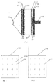
- Fig. 1 illustrates a displayer module 1 of a display device with a camera function provided in a preferred embodiment of the present disclosure.
- the displayer module 1 includes an upper substrate assembly 11, a liquid crystal layer 12, a lower substrate assembly 13, a backlight module 14 and a driving circuit unit 15 arranged in sequence.
- the upper substrate assembly 11 includes an upper polarizer 111, an upper glass substrate 112 and a filter 113 arranged in sequence.
- the lower substrate assembly 13 includes a lower glass substrate 131, a TFT array 132 and a lower polarizer 133 arranged in sequence.
- the liquid crystal layer 12 is filled between the upper substrate assembly 11 and the lower substrate assembly 13.
- the working principle of the displayer module 1 is similar to that of a liquid crystal display in the related art.
- a TFT switch is controlled via a voltage at each pixel located at each row and column, such that a rotate degree of liquid crystal molecule may be controlled so as to control a display degree of each RGB sub pixel, thereby generating an image.
- a camera module 2 is integrated in the displayer module 1.
- the camera module 2 may include a plurality of camera sub-modules installed at intervals on a surface of the displayer module 1.
- Each camera sub-module of the camera module 2 is configured to shoot an image of a region above the display screen and directly facing the camera sub-module.
- the camera module 2 includes a plurality of lens units 21, a plurality of photosensitive units 22 matched with the plurality of lens units 21 respectively, and a set of image processing chips 23.
- the set of image processing chips 23 is configured to process images generated by the camera module 2 and to output a processed image.
- the set of image processing chips 23 is integrated in the driving circuit unit 15.
- the set of image processing chips 23 may include a driving chip configured for image recognition, more specifically and optionally, a CMOS-LCD driving chip.
- the set of image processing chips 23 further includes an image overlaying and processing chip configured for image overlaying and post-processing, more specifically and optionally, a VGA control chip. After a processing of such a chip, an overlay process is performed on images shot by all the photosensitive units 22 and a complete image may be typically acquired. An equivalent shooting angle of this complete image may be directly facing the display screen. Thus, this image is equivalent to an image photographed by a camera at the center of display screen from an angle perpendicular to the display screen. Since a photosensitive unit 22 for imaging includes a plurality of photosensitive pixels, the image generated after the processing has a more clear and comprehensive display effect than an image photographed by a conventional single camera.
- images photographed by some photosensitive units 22 at some certain positions may be selected to be overlaid so as to generate a complete image.
- images photographed by photosensitive pixels at different positions may be acquired and overlaid so as to generate images at different shooting positions and angles.
- Fig. 2-1 is a schematic diagram of a structure of a filter 113 shown in Fig. 1
- Fig. 2-2 is a schematic diagram of a structure of an upper glass substrate 112 and a plurality of lens units 21 corresponding to the filter 113.
- the position of the filter 113 is matched with the position of the upper glass substrate 112, and the plurality of lens units 21 on the upper glass substrate 112 correspond to the plurality of photosensitive units 22 on the filter 113 respectively.
- the filter 113 includes a pixel area 1131 and a plurality of photosensitive units 22.
- the filter 113 includes a pixel area 1131 and a plurality of photosensitive units 22.
- the plurality of photosensitive units 22 are fixed on the filter 113 and disposed at intervals in the pixel area 1131.
- the pixel area 1131 is configured to form pixels, which consists of RGB arrays.
- the plurality of photosensitive units 22 are discretely distributed in the pixel area 1131.
- the arrangement of the plurality of photosensitive units 22 may be designed as needed. Considering the imaging requirement, the plurality of photosensitive units 22 may be designed in a way that they are uniformly disposed on a whole surface of the filter 113, such that a better imaging effect may be obtained.
- the plurality of lens units 21 are disposed on the upper glass substrate 112 and correspond to the plurality of photosensitive units 22 respectively.
- the plurality of lens units 21 are also uniformly disposed on the whole surface of the glass substrate 112.
- Such design is equivalent to that a plurality of micro cameras are discretely disposed on the surface of display screen, such that the images of the region directly facing the display screen may be photographed from several angles and then may be subsequently processed by the set of image processing chips 23, so as to acquire a composite image with a high quality.
- a user uses this display screen to conduct a video chat, a video image as if the pupils of the user direct to the camera may be obtained if the user looks at the center of display screen.
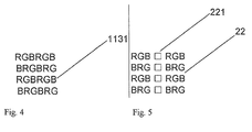
- Fig. 3 is a schematic diagram of a structure of the pixel area 1131 and the plurality of photosensitive units 22 shown in Fig. 2 .
- the pixel area 1131 only includes RGB arrays.
- the plurality of photosensitive units 22 include RGB arrays and photosensitive points 221.
- the photosensitive points and the RGB arrays are disposed alternatively.
- the RGB array is similar to that in an existing liquid crystal display and the photosensitive point may consist of a thin layer of photosensitive material.
- silver salt photosensitive material such as silver halide grain may be chosen and used.
- Fig. 4 is a flow chart showing a method for shooting and displaying an image in the display screen shown in Fig. 1 .
- step S1 the display device shown in Fig. 1 is provided and function of shoot is started.
- step S2 the light from an object facing a display screen of the display device passes through the upper polarizer 111, enters the plurality of lens units 21, and then enters the plurality of photosensitive units 22 after being focused by the plurality of lens units 21, such that images may be generated and inputted into the set of image processing chips 23.
- step S3 an image recognition and overlaying process is performed on the images by the set of image processing chips 23, so as to acquire a complete composite image.
- step S4 a smooth transition process is performed on the composite image by the set of image processing chips 23.
- step S5 the processed composite image is outputted and displayed using the displayer module 1 of the display device shown in Fig. 1 , such that a video image of the region directly facing the display screen may be obtained in the display screen.
- the displayer module before outputting and displaying the image, it is determined whether the display device is displaying another image. If the display device is not displaying another image when shooting, the displayer module outputs the processed composite image to the center of screen of the display device for displaying.
- the display device If the display device is displaying another image when shooting, the display window of the displayed image is zoomed out and arranged at a corner of screen of the display device. Then, the displayer module outputs the processed composite image to the center of screen of the display device for displaying.
- a display with a camera function is typically provided with a front camera which is generally disposed at an upper of the display.
- a front camera which is generally disposed at an upper of the display.
- a plurality of micro photosensitive imaging units are discretely disposed on a surface of a display screen, such that an object directly facing the display screen may be photographed from several angles, and then a composite image with high quality may be acquired after post-processing.
- a user uses the display device according to the present disclosure to conduct a video chat, a video image as if the pupils of the user direct to the camera may be obtained if the user looks at the center of display screen, such that problems existing in the related art may be solved.
Landscapes
- Physics & Mathematics (AREA)
- Engineering & Computer Science (AREA)
- Multimedia (AREA)
- Signal Processing (AREA)
- Nonlinear Science (AREA)
- Crystallography & Structural Chemistry (AREA)
- Mathematical Physics (AREA)
- Chemical & Material Sciences (AREA)
- General Physics & Mathematics (AREA)
- Optics & Photonics (AREA)
- Human Computer Interaction (AREA)
- Spectroscopy & Molecular Physics (AREA)
- Microelectronics & Electronic Packaging (AREA)
- Studio Devices (AREA)
- Devices For Indicating Variable Information By Combining Individual Elements (AREA)
Abstract
Description
- This application is based on and claims priority to Chinese Patent Application No.
201310608258.5 - The present disclosure relates to the electronic device field, and more particularly, to a display device and a method for shooting and displaying an image.
- In the related art, a display with a camera function is typically provided with a front camera which is generally disposed at an upper part of the display. When a user takes a selfie using such a display with the front camera, he needs to look steadily at the front camera so as to acquire a photo with high quality. In this case, the user cannot gaze at the screen to observe effect of the selfie at the same time. However, if the user moves eyes from the front camera and looks steadily at the screen, a selfie with high quality cannot be acquired.
- An objective of the present disclosure is to solve the above problems of the existing display screen, and to provide a display device with a camera function, in which a plurality of micro photosensitive imaging units are discretely disposed on a surface of a display screen, such that an object directly facing the display screen may be photographed from several angels and then a composite image with high quality may be acquired by a further subsequent processing.
- The technical solution adopted by the present disclosure for solving the technical problems may be described as follows.
- A display device is provided to include a displayer module and a camera module installed in the displayer module and configured to shoot images of an external object directly facing the displayer module, the camera module includes a plurality of lens units installed at intervals on a surface of the displayer module, a plurality of photosensitive units matched with the plurality of lens units respectively, and a set of image processing chips configured to process the images generated by the camera module.
- Alternatively, the displayer module includes an upper substrate assembly, a liquid crystal layer, a lower substrate assembly and a backlight module arranged in sequence, wherein, the upper substrate assembly includes an upper polarizer, an upper glass substrate and a filter arranged in sequence; the lower substrate assembly includes a lower glass substrate, a TFT (thin film transistor) array and a lower polarizer arranged in sequence; and the liquid crystal layer is filled between the upper substrate assembly and the lower substrate assembly.
- Alternatively, the display device further includes: a driving circuit unit, configured to supply power to drive respective parts in the display device.
- Alternatively, the set of image processing chips is integrated in the driving circuit unit.
- Alternatively, the set of image processing chips includes: an image recognizing chip configured for image recognition; and an image overlaying and processing chip configured for image overlaying and post-processing.
- Alternatively, the plurality of photosensitive units are connected to the image recognizing chip, and the image recognizing chip is connected to the image overlaying and processing chip.
- Alternatively, the filter includes a pixel area configured to form pixels, the plurality of photosensitive units are fixed on the filter and disposed at intervals in the pixel area.
- Alternatively, the plurality of lens units are disposed on the upper glass substrate and correspond to the plurality of photosensitive units on the filter respectively.
- There is also provided a method for shooting and displaying an image, including the following steps:
- S1, providing the display device described above, and starting function of shoot;
- S2, generating images by the plurality of photosensitive units, by making light emitted from an object facing the display device pass through the polarizer, enter the plurality of lens units and enter the plurality of photosensitive units, and inputting the images into the set of image processing chips;
- S3, performing an overlaying process on the images by the set of image processing chips to acquire a complete composite image;
- S4, performing a smooth transition process on the composite image by the set of image processing chips; and
- S5, outputting and displaying the processed composite image by the displayer module.
- Step S5 may further include the following optional sub-steps:
- S5A, if the display device is not displaying another image when shooting, outputting by the displayer module the processed composite image to a center of a screen of the display device for displaying;
- S5B, if the display device is displaying another image when shooting, zooming in a display window of the image displayed and arranging the display window at a corner of the screen of the display device, and outputting by the displayer module the processed composite image to a center of a screen of the display device for displaying.
- In the display device with a camera function according to embodiments of the present disclosure, a plurality of micro photosensitive imaging units are discretely disposed on a surface of a display screen, such that an object directly facing the display screen may be photographed from several angles, and then a composite image with high quality may be acquired after post-processing. When a user uses the display device according to the present disclosure to conduct a video chat, a video image as if the pupils of the user direct to the camera may be obtained if the user looks at the center of display screen, such that problems existing in the related art may be solved.
- In order to make the technical solutions of embodiments of the present invention more clearly, the accompanying drawings used in the description of embodiments of the present invention are briefly described hereunder. Obviously, the described drawings are merely some embodiments of present invention. For persons skilled in the art, other drawings may be obtained based on these drawings without any creative work.
-
Fig. 1 is a section view of a display device according to a preferred embodiment of the present disclosure. -
Fig. 2 is a schematic diagram of a surface structure of a filter in the display device shown inFig. 1 . -
Fig. 3 is a schematic diagram of a structure of an upper glass substrate and a plurality of lens units in the display device shown inFig. 1 . -
Fig. 4 is a schematic diagram of a pixel area shown inFig. 2 . -
Fig. 5 is a schematic diagram of a plurality of photosensitive units shown inFig. 2 . -
Fig. 6 is a flow chart of a method for shooting and displaying an image in the display device shown inFig. 1 . - To make the objectives, the technical solutions, and the advantages of embodiments of the present invention clearer, the technical solutions in embodiments of the present invention are hereinafter described clearly and completely with reference to the accompanying drawings in embodiments of the present invention. Apparently, the described embodiments are merely a part of embodiments of the present invention, rather than all embodiments of the present invention. All other embodiments obtained by persons of ordinary skill in the art based on embodiments of the present invention without creative efforts shall fall within the protection scope of the present invention.
-
Fig. 1 illustrates adisplayer module 1 of a display device with a camera function provided in a preferred embodiment of the present disclosure. As shown inFig. 1 , thedisplayer module 1 includes an upper substrate assembly 11, aliquid crystal layer 12, alower substrate assembly 13, abacklight module 14 and adriving circuit unit 15 arranged in sequence. Wherein, the upper substrate assembly 11 includes anupper polarizer 111, anupper glass substrate 112 and afilter 113 arranged in sequence. Thelower substrate assembly 13 includes alower glass substrate 131, aTFT array 132 and alower polarizer 133 arranged in sequence. Theliquid crystal layer 12 is filled between the upper substrate assembly 11 and thelower substrate assembly 13. - As a preferred implementation, the working principle of the
displayer module 1 is similar to that of a liquid crystal display in the related art. A TFT switch is controlled via a voltage at each pixel located at each row and column, such that a rotate degree of liquid crystal molecule may be controlled so as to control a display degree of each RGB sub pixel, thereby generating an image. - A camera module 2 is integrated in the
displayer module 1. As a preferred implementation, the camera module 2 may include a plurality of camera sub-modules installed at intervals on a surface of thedisplayer module 1. Each camera sub-module of the camera module 2 is configured to shoot an image of a region above the display screen and directly facing the camera sub-module. The camera module 2 includes a plurality oflens units 21, a plurality ofphotosensitive units 22 matched with the plurality oflens units 21 respectively, and a set of image processing chips 23. The set of image processing chips 23 is configured to process images generated by the camera module 2 and to output a processed image. - As a preferred embodiment of a preferred implementation, the set of image processing chips 23 is integrated in the
driving circuit unit 15. The set of image processing chips 23 may include a driving chip configured for image recognition, more specifically and optionally, a CMOS-LCD driving chip. - The set of image processing chips 23 further includes an image overlaying and processing chip configured for image overlaying and post-processing, more specifically and optionally, a VGA control chip. After a processing of such a chip, an overlay process is performed on images shot by all the
photosensitive units 22 and a complete image may be typically acquired. An equivalent shooting angle of this complete image may be directly facing the display screen. Thus, this image is equivalent to an image photographed by a camera at the center of display screen from an angle perpendicular to the display screen. Since aphotosensitive unit 22 for imaging includes a plurality of photosensitive pixels, the image generated after the processing has a more clear and comprehensive display effect than an image photographed by a conventional single camera. - As another preferred implementation, images photographed by some
photosensitive units 22 at some certain positions may be selected to be overlaid so as to generate a complete image. By selectingphotosensitive units 22 at different positions, images photographed by photosensitive pixels at different positions may be acquired and overlaid so as to generate images at different shooting positions and angles. - Referring to
Fig. 2, Fig. 2-1 is a schematic diagram of a structure of afilter 113 shown inFig. 1, and Fig. 2-2 is a schematic diagram of a structure of anupper glass substrate 112 and a plurality oflens units 21 corresponding to thefilter 113. The position of thefilter 113 is matched with the position of theupper glass substrate 112, and the plurality oflens units 21 on theupper glass substrate 112 correspond to the plurality ofphotosensitive units 22 on thefilter 113 respectively. - In
Fig. 2-1 , thefilter 113 includes apixel area 1131 and a plurality ofphotosensitive units 22. - As a preferred embodiment, the
filter 113 includes apixel area 1131 and a plurality ofphotosensitive units 22. The plurality ofphotosensitive units 22 are fixed on thefilter 113 and disposed at intervals in thepixel area 1131. Thepixel area 1131 is configured to form pixels, which consists of RGB arrays. As a preferred implementation, the plurality ofphotosensitive units 22 are discretely distributed in thepixel area 1131. The arrangement of the plurality ofphotosensitive units 22 may be designed as needed. Considering the imaging requirement, the plurality ofphotosensitive units 22 may be designed in a way that they are uniformly disposed on a whole surface of thefilter 113, such that a better imaging effect may be obtained. - In
Fig. 2-2 , the plurality oflens units 21 are disposed on theupper glass substrate 112 and correspond to the plurality ofphotosensitive units 22 respectively. When the plurality ofphotosensitive units 22 are uniformly disposed on the whole surface of thefilter 113, the plurality oflens units 21 are also uniformly disposed on the whole surface of theglass substrate 112. Such design is equivalent to that a plurality of micro cameras are discretely disposed on the surface of display screen, such that the images of the region directly facing the display screen may be photographed from several angles and then may be subsequently processed by the set of image processing chips 23, so as to acquire a composite image with a high quality. When a user uses this display screen to conduct a video chat, a video image as if the pupils of the user direct to the camera may be obtained if the user looks at the center of display screen. -
Fig. 3 is a schematic diagram of a structure of thepixel area 1131 and the plurality ofphotosensitive units 22 shown inFig. 2 . Thepixel area 1131 only includes RGB arrays. The plurality ofphotosensitive units 22 include RGB arrays andphotosensitive points 221. The photosensitive points and the RGB arrays are disposed alternatively. As a preferred embodiment, the RGB array is similar to that in an existing liquid crystal display and the photosensitive point may consist of a thin layer of photosensitive material. As a preferred implementation, silver salt photosensitive material such as silver halide grain may be chosen and used. -
Fig. 4 is a flow chart showing a method for shooting and displaying an image in the display screen shown inFig. 1 . - In step S1, the display device shown in
Fig. 1 is provided and function of shoot is started. - In step S2, the light from an object facing a display screen of the display device passes through the
upper polarizer 111, enters the plurality oflens units 21, and then enters the plurality ofphotosensitive units 22 after being focused by the plurality oflens units 21, such that images may be generated and inputted into the set of image processing chips 23. - In step S3, an image recognition and overlaying process is performed on the images by the set of image processing chips 23, so as to acquire a complete composite image.
- In step S4, a smooth transition process is performed on the composite image by the set of image processing chips 23.
- In step S5, the processed composite image is outputted and displayed using the
displayer module 1 of the display device shown inFig. 1 , such that a video image of the region directly facing the display screen may be obtained in the display screen. As a preferred implementation, before outputting and displaying the image, it is determined whether the display device is displaying another image. If the display device is not displaying another image when shooting, the displayer module outputs the processed composite image to the center of screen of the display device for displaying. - If the display device is displaying another image when shooting, the display window of the displayed image is zoomed out and arranged at a corner of screen of the display device. Then, the displayer module outputs the processed composite image to the center of screen of the display device for displaying.
- In the related art, a display with a camera function is typically provided with a front camera which is generally disposed at an upper of the display. When a user takes a selfie using such a display with a front camera, he needs to look steadily at the front camera so as to acquire a selfie with high quality. In this case, the user cannot gaze at the screen to observe effect of the selfie at the same time. However, if the user moves eyes from the front camera and looks steadily at the screen, a photo with high quality cannot be acquired.
- In the display device with a camera function according to embodiments of the present disclosure, a plurality of micro photosensitive imaging units are discretely disposed on a surface of a display screen, such that an object directly facing the display screen may be photographed from several angles, and then a composite image with high quality may be acquired after post-processing. When a user uses the display device according to the present disclosure to conduct a video chat, a video image as if the pupils of the user direct to the camera may be obtained if the user looks at the center of display screen, such that problems existing in the related art may be solved.
- Since the foregoing description as directed only to a preferred embodiment of the invention, various changes and modifications apparent to those skilled in the art, can be made to these features and embodiments without departing from the spirit and scope of the present disclosure. Moreover, under the guidance of the present disclosure, various modifications may be made to these features and embodiments to adapt to specific situations and materials, without departing from the spirit and scope of the present disclosure. Thus, the present disclosure is not limited to the specific embodiments described herein. All embodiments falling within the scope of claims of the present disclosure shall fall within the protection scope of the present disclosure.
Claims (10)
- A display device, comprising a displayer module, and being characterized at: the display device further comprises a camera module installed in the displayer module and configured to shoot images of an external object directly facing the displayer module, and the camera module comprises:a plurality of lens units, installed at intervals on a surface of the displayer module;a plurality of photosensitive units, matched with the plurality of lens units respectively; anda set of image processing chips, configured to process the images generated by the camera module.
- The display device according to claim 1, being characterized at that: the displayer module comprises an upper substrate assembly, a liquid crystal layer, a lower substrate assembly and a backlight module arranged in sequence;
the upper substrate assembly comprises an upper polarizer, an upper glass substrate and a filter arranged in sequence;
the lower substrate assembly comprises a lower glass substrate, a TFT array and a lower polarizer arranged in sequence;
the liquid crystal layer is filled between the upper substrate assembly and the lower substrate assembly. - The display device according to claim 2, being characterized at that: the display device further comprises:a driving circuit unit, configured to supply power to drive respective parts in the display device.
- The display device according to claim 3, being characterized at that: the set of image processing chips is integrated in the driving circuit unit.
- The display device according to claim 4, being characterized at that: the set of image processing chips comprises:an image recognizing chip, configured for image recognition; andan image overlaying and processing chip, configured for image overlaying and post-processing.
- The display device according to claim 5, being characterized at that: the plurality of photosensitive units are connected to the image recognizing chip, and the image recognizing chip is connected to the image overlaying and processing chip.
- The display device according to claim 2, being characterized at that: the filter comprises a pixel area configured to form pixels, and the plurality of photosensitive units are fixed on the filter and disposed at intervals in the pixel area.
- The display device according to claim 2, being characterized at that: the plurality of lens units are disposed on the upper glass substrate and correspond to the plurality of photosensitive units on the filter respectively.
- A method for shooting and displaying an image, being characterized at that: the method comprises:S1, providing the display device according to any one of claims 1-8, and starting function of shoot;S2, generating images by the plurality of photosensitive units, by making light from an object facing the display device pass through the polarizer, enter the plurality of lens units and enter the plurality of photosensitive units, and inputting the images into the set of image processing chips;S3, performing an overlaying process on the images by the set of image processing chips to acquire a complete composite image;S4, performing a smooth transition process on the composite image by the set of image processing chips; andS5, outputting and displaying the processed composite image by the displayer module.
- The method according to claim 9, being characterized at that: step S5 further comprises the following optional sub-steps:S5A, if the display device is not displaying another image when shooting, outputting by the displayer module the processed composite image to a center of a screen of the display device for displaying;S5B, if the display device is displaying another image when shooting, zooming out a display window of the image displayed and arranging the display window at a corner of the screen of the display device, and outputting by the displayer module the processed composite image to a center of a screen of the display device for displaying.
Applications Claiming Priority (2)
| Application Number | Priority Date | Filing Date | Title |
|---|---|---|---|
| CN201310608258.5A CN103780812A (en) | 2013-11-26 | 2013-11-26 | Display apparatus and shooting display method thereof |
| PCT/CN2014/088203 WO2015078236A1 (en) | 2013-11-26 | 2014-10-09 | Display device and shooting display method therefor |
Publications (3)
| Publication Number | Publication Date |
|---|---|
| EP3076653A1 true EP3076653A1 (en) | 2016-10-05 |
| EP3076653A4 EP3076653A4 (en) | 2017-06-14 |
| EP3076653B1 EP3076653B1 (en) | 2019-06-26 |
Family
ID=50572605
Family Applications (1)
| Application Number | Title | Priority Date | Filing Date |
|---|---|---|---|
| EP14866148.1A Not-in-force EP3076653B1 (en) | 2013-11-26 | 2014-10-09 | Display device and shooting display method therefor |
Country Status (5)
| Country | Link |
|---|---|
| US (1) | US9692986B2 (en) |
| EP (1) | EP3076653B1 (en) |
| CN (1) | CN103780812A (en) |
| ES (1) | ES2737625T3 (en) |
| WO (1) | WO2015078236A1 (en) |
Families Citing this family (13)
| Publication number | Priority date | Publication date | Assignee | Title |
|---|---|---|---|---|
| CN103780812A (en) | 2013-11-26 | 2014-05-07 | 广东欧珀移动通信有限公司 | Display apparatus and shooting display method thereof |
| CN104320589B (en) * | 2014-11-10 | 2017-12-29 | 联想(北京)有限公司 | A kind of image collecting device, method and electronic equipment |
| CN105791671B (en) * | 2014-12-26 | 2021-04-02 | 中兴通讯股份有限公司 | A method, device and terminal for shooting and correcting front camera |
| CN104539833A (en) | 2015-01-07 | 2015-04-22 | 京东方科技集团股份有限公司 | Electronic equipment |
| CN106710524A (en) * | 2015-11-13 | 2017-05-24 | 小米科技有限责任公司 | OLED panel, terminal and photosensitive control method |
| CN106019671B (en) * | 2016-07-22 | 2023-12-22 | 杨永建 | Unit, assembly and board integrating display and camera shooting |
| CN106603772B (en) * | 2017-01-26 | 2019-12-27 | Oppo广东移动通信有限公司 | Electronic device and image acquisition method |
| CN108712526A (en) * | 2018-04-28 | 2018-10-26 | 维沃移动通信有限公司 | A kind of screen and mobile terminal |
| CN108600472A (en) * | 2018-07-18 | 2018-09-28 | 苏州天为幕烟花科技有限公司 | A kind of mobile phone of the complementary realization of dot matrix shields technology comprehensively |
| CN108989497A (en) * | 2018-07-18 | 2018-12-11 | 苏州天为幕烟花科技有限公司 | A kind of discoloration backlight shields technology comprehensively |
| CN108965684A (en) * | 2018-09-28 | 2018-12-07 | 出门问问信息科技有限公司 | Electronic equipment |
| CN113452813B (en) * | 2020-03-27 | 2022-11-11 | 北京小米移动软件有限公司 | Image acquisition device, terminal device, method, processing device, and medium |
| CN116320674A (en) * | 2023-02-15 | 2023-06-23 | 京东方科技集团股份有限公司 | Eye image acquisition device, acquisition method and virtual reality equipment |
Family Cites Families (13)
| Publication number | Priority date | Publication date | Assignee | Title |
|---|---|---|---|---|
| JPH0846162A (en) * | 1994-07-29 | 1996-02-16 | Fujitsu Ltd | Display / imaging device |
| US8508508B2 (en) * | 2003-02-14 | 2013-08-13 | Next Holdings Limited | Touch screen signal processing with single-point calibration |
| JP4616559B2 (en) * | 2004-01-15 | 2011-01-19 | 大日本印刷株式会社 | Display device and display system |
| CN101119435A (en) | 2006-08-01 | 2008-02-06 | 王清山 | Electronic display apparatus and manufacturing method therefor |
| WO2009091568A2 (en) * | 2008-01-14 | 2009-07-23 | Sina Fateh | System and method for improving the peripheral vision of a subject |
| DE112008003983T5 (en) * | 2008-09-15 | 2011-07-21 | Hewlett-Packard Development Co., L.P., Tex. | Touch screen display with multiple cameras |
| US8223188B2 (en) * | 2008-09-16 | 2012-07-17 | Alcatel Lucent | Monitor having integral camera and method of operating the same |
| US8654234B2 (en) * | 2009-07-26 | 2014-02-18 | Massachusetts Institute Of Technology | Bi-directional screen |
| CN102348091B (en) * | 2010-07-30 | 2014-12-31 | 联想(北京)有限公司 | Display screen and terminal apparatus using the same |
| KR20120080845A (en) * | 2011-01-10 | 2012-07-18 | 삼성전자주식회사 | Oled display apparatus having optical sensing funtion |
| CN202696751U (en) | 2012-01-05 | 2013-01-23 | 鼎创电子股份有限公司 | Real-time integration system of multi-lens images |
| CN103780812A (en) | 2013-11-26 | 2014-05-07 | 广东欧珀移动通信有限公司 | Display apparatus and shooting display method thereof |
| JP6558088B2 (en) * | 2015-06-12 | 2019-08-14 | リコーイメージング株式会社 | Imaging apparatus, imaging control apparatus, and imaging control method |
-
2013
- 2013-11-26 CN CN201310608258.5A patent/CN103780812A/en active Pending
-
2014
- 2014-10-09 US US15/039,330 patent/US9692986B2/en active Active
- 2014-10-09 EP EP14866148.1A patent/EP3076653B1/en not_active Not-in-force
- 2014-10-09 WO PCT/CN2014/088203 patent/WO2015078236A1/en not_active Ceased
- 2014-10-09 ES ES14866148T patent/ES2737625T3/en active Active
Also Published As
| Publication number | Publication date |
|---|---|
| CN103780812A (en) | 2014-05-07 |
| US9692986B2 (en) | 2017-06-27 |
| ES2737625T3 (en) | 2020-01-15 |
| EP3076653B1 (en) | 2019-06-26 |
| WO2015078236A1 (en) | 2015-06-04 |
| EP3076653A4 (en) | 2017-06-14 |
| US20170142342A1 (en) | 2017-05-18 |
Similar Documents
| Publication | Publication Date | Title |
|---|---|---|
| US9692986B2 (en) | Display device and method for shooting and displaying images | |
| JP6246292B2 (en) | OLED display device with light detection function | |
| US8891030B2 (en) | Display method, display apparatus, optical unit, method of manufacturing display apparatus, and electronic equipment | |
| US20200106939A1 (en) | Display panel, display device and image acquiring method thereof | |
| CN109001935B (en) | Liquid crystal display device having a light shielding layer | |
| US20110279689A1 (en) | Integrated Display Camera Using Oscillating Display Elements | |
| US20190035364A1 (en) | Display apparatus, method of driving display apparatus, and electronic apparatus | |
| JP2010015015A (en) | Electro-optical device and electronic equipment | |
| US9857601B2 (en) | Display device | |
| JPWO2016038997A1 (en) | Display device, driving method of display device, and electronic apparatus | |
| US20140063052A1 (en) | Transparent display apparatus and method of driving the same | |
| EP3346308A1 (en) | Detection device, detection method, detection program, and imaging device | |
| JP2022059450A (en) | Display, photoelectric conversion device, electronic apparatus, illumination device, movable body, and wearable device | |
| JP5942130B2 (en) | Display device | |
| US20090079685A1 (en) | Liquid crystal display device, method for driving liquid crystal display device, and electronic apparatus | |
| US11184526B2 (en) | Electronic apparatus and control method thereof | |
| US9846303B2 (en) | Display system having display device and sensor on substrate | |
| JP5230910B2 (en) | Transmission type display device | |
| CN111627335B (en) | A display panel and display device | |
| JP5144006B2 (en) | Camera with display screen | |
| US11209703B2 (en) | Display device | |
| JP7807901B2 (en) | Display device, photoelectric conversion device and electronic device | |
| JP2003101825A (en) | Lens information display device | |
| EP3016381A1 (en) | Video conferencing system | |
| US20140118559A1 (en) | Modular Display Camera |
Legal Events
| Date | Code | Title | Description |
|---|---|---|---|
| PUAI | Public reference made under article 153(3) epc to a published international application that has entered the european phase |
Free format text: ORIGINAL CODE: 0009012 |
|
| 17P | Request for examination filed |
Effective date: 20160519 |
|
| AK | Designated contracting states |
Kind code of ref document: A1 Designated state(s): AL AT BE BG CH CY CZ DE DK EE ES FI FR GB GR HR HU IE IS IT LI LT LU LV MC MK MT NL NO PL PT RO RS SE SI SK SM TR |
|
| AX | Request for extension of the european patent |
Extension state: BA ME |
|
| DAX | Request for extension of the european patent (deleted) | ||
| A4 | Supplementary search report drawn up and despatched |
Effective date: 20170512 |
|
| RIC1 | Information provided on ipc code assigned before grant |
Ipc: H04N 5/225 20060101AFI20170508BHEP |
|
| STAA | Information on the status of an ep patent application or granted ep patent |
Free format text: STATUS: EXAMINATION IS IN PROGRESS |
|
| 17Q | First examination report despatched |
Effective date: 20171221 |
|
| RAP1 | Party data changed (applicant data changed or rights of an application transferred) |
Owner name: GUANGDONG OPPO MOBILE TELECOMMUNICATIONS CORP., LT |
|
| GRAP | Despatch of communication of intention to grant a patent |
Free format text: ORIGINAL CODE: EPIDOSNIGR1 |
|
| STAA | Information on the status of an ep patent application or granted ep patent |
Free format text: STATUS: GRANT OF PATENT IS INTENDED |
|
| INTG | Intention to grant announced |
Effective date: 20190222 |
|
| RIN1 | Information on inventor provided before grant (corrected) |
Inventor name: ZHANG, WEIZHENG |
|
| GRAS | Grant fee paid |
Free format text: ORIGINAL CODE: EPIDOSNIGR3 |
|
| GRAA | (expected) grant |
Free format text: ORIGINAL CODE: 0009210 |
|
| STAA | Information on the status of an ep patent application or granted ep patent |
Free format text: STATUS: THE PATENT HAS BEEN GRANTED |
|
| AK | Designated contracting states |
Kind code of ref document: B1 Designated state(s): AL AT BE BG CH CY CZ DE DK EE ES FI FR GB GR HR HU IE IS IT LI LT LU LV MC MK MT NL NO PL PT RO RS SE SI SK SM TR |
|
| REG | Reference to a national code |
Ref country code: GB Ref legal event code: FG4D |
|
| REG | Reference to a national code |
Ref country code: CH Ref legal event code: EP |
|
| REG | Reference to a national code |
Ref country code: AT Ref legal event code: REF Ref document number: 1149679 Country of ref document: AT Kind code of ref document: T Effective date: 20190715 |
|
| REG | Reference to a national code |
Ref country code: DE Ref legal event code: R096 Ref document number: 602014049262 Country of ref document: DE |
|
| REG | Reference to a national code |
Ref country code: IE Ref legal event code: FG4D |
|
| REG | Reference to a national code |
Ref country code: NL Ref legal event code: FP |
|
| PG25 | Lapsed in a contracting state [announced via postgrant information from national office to epo] |
Ref country code: AL Free format text: LAPSE BECAUSE OF FAILURE TO SUBMIT A TRANSLATION OF THE DESCRIPTION OR TO PAY THE FEE WITHIN THE PRESCRIBED TIME-LIMIT Effective date: 20190626 Ref country code: NO Free format text: LAPSE BECAUSE OF FAILURE TO SUBMIT A TRANSLATION OF THE DESCRIPTION OR TO PAY THE FEE WITHIN THE PRESCRIBED TIME-LIMIT Effective date: 20190926 Ref country code: FI Free format text: LAPSE BECAUSE OF FAILURE TO SUBMIT A TRANSLATION OF THE DESCRIPTION OR TO PAY THE FEE WITHIN THE PRESCRIBED TIME-LIMIT Effective date: 20190626 Ref country code: SE Free format text: LAPSE BECAUSE OF FAILURE TO SUBMIT A TRANSLATION OF THE DESCRIPTION OR TO PAY THE FEE WITHIN THE PRESCRIBED TIME-LIMIT Effective date: 20190626 Ref country code: HR Free format text: LAPSE BECAUSE OF FAILURE TO SUBMIT A TRANSLATION OF THE DESCRIPTION OR TO PAY THE FEE WITHIN THE PRESCRIBED TIME-LIMIT Effective date: 20190626 Ref country code: LT Free format text: LAPSE BECAUSE OF FAILURE TO SUBMIT A TRANSLATION OF THE DESCRIPTION OR TO PAY THE FEE WITHIN THE PRESCRIBED TIME-LIMIT Effective date: 20190626 |
|
| REG | Reference to a national code |
Ref country code: LT Ref legal event code: MG4D |
|
| PG25 | Lapsed in a contracting state [announced via postgrant information from national office to epo] |
Ref country code: RS Free format text: LAPSE BECAUSE OF FAILURE TO SUBMIT A TRANSLATION OF THE DESCRIPTION OR TO PAY THE FEE WITHIN THE PRESCRIBED TIME-LIMIT Effective date: 20190626 Ref country code: GR Free format text: LAPSE BECAUSE OF FAILURE TO SUBMIT A TRANSLATION OF THE DESCRIPTION OR TO PAY THE FEE WITHIN THE PRESCRIBED TIME-LIMIT Effective date: 20190927 Ref country code: BG Free format text: LAPSE BECAUSE OF FAILURE TO SUBMIT A TRANSLATION OF THE DESCRIPTION OR TO PAY THE FEE WITHIN THE PRESCRIBED TIME-LIMIT Effective date: 20190926 Ref country code: LV Free format text: LAPSE BECAUSE OF FAILURE TO SUBMIT A TRANSLATION OF THE DESCRIPTION OR TO PAY THE FEE WITHIN THE PRESCRIBED TIME-LIMIT Effective date: 20190626 |
|
| RAP2 | Party data changed (patent owner data changed or rights of a patent transferred) |
Owner name: GUANGDONG OPPO MOBILE TELECOMMUNICATIONS CORP., LT |
|
| REG | Reference to a national code |
Ref country code: ES Ref legal event code: FG2A Ref document number: 2737625 Country of ref document: ES Kind code of ref document: T3 Effective date: 20200115 Ref country code: AT Ref legal event code: MK05 Ref document number: 1149679 Country of ref document: AT Kind code of ref document: T Effective date: 20190626 |
|
| PG25 | Lapsed in a contracting state [announced via postgrant information from national office to epo] |
Ref country code: CZ Free format text: LAPSE BECAUSE OF FAILURE TO SUBMIT A TRANSLATION OF THE DESCRIPTION OR TO PAY THE FEE WITHIN THE PRESCRIBED TIME-LIMIT Effective date: 20190626 Ref country code: SK Free format text: LAPSE BECAUSE OF FAILURE TO SUBMIT A TRANSLATION OF THE DESCRIPTION OR TO PAY THE FEE WITHIN THE PRESCRIBED TIME-LIMIT Effective date: 20190626 Ref country code: RO Free format text: LAPSE BECAUSE OF FAILURE TO SUBMIT A TRANSLATION OF THE DESCRIPTION OR TO PAY THE FEE WITHIN THE PRESCRIBED TIME-LIMIT Effective date: 20190626 Ref country code: AT Free format text: LAPSE BECAUSE OF FAILURE TO SUBMIT A TRANSLATION OF THE DESCRIPTION OR TO PAY THE FEE WITHIN THE PRESCRIBED TIME-LIMIT Effective date: 20190626 Ref country code: EE Free format text: LAPSE BECAUSE OF FAILURE TO SUBMIT A TRANSLATION OF THE DESCRIPTION OR TO PAY THE FEE WITHIN THE PRESCRIBED TIME-LIMIT Effective date: 20190626 Ref country code: PT Free format text: LAPSE BECAUSE OF FAILURE TO SUBMIT A TRANSLATION OF THE DESCRIPTION OR TO PAY THE FEE WITHIN THE PRESCRIBED TIME-LIMIT Effective date: 20191028 |
|
| PG25 | Lapsed in a contracting state [announced via postgrant information from national office to epo] |
Ref country code: IS Free format text: LAPSE BECAUSE OF FAILURE TO SUBMIT A TRANSLATION OF THE DESCRIPTION OR TO PAY THE FEE WITHIN THE PRESCRIBED TIME-LIMIT Effective date: 20191026 Ref country code: SM Free format text: LAPSE BECAUSE OF FAILURE TO SUBMIT A TRANSLATION OF THE DESCRIPTION OR TO PAY THE FEE WITHIN THE PRESCRIBED TIME-LIMIT Effective date: 20190626 |
|
| PG25 | Lapsed in a contracting state [announced via postgrant information from national office to epo] |
Ref country code: TR Free format text: LAPSE BECAUSE OF FAILURE TO SUBMIT A TRANSLATION OF THE DESCRIPTION OR TO PAY THE FEE WITHIN THE PRESCRIBED TIME-LIMIT Effective date: 20190626 |
|
| PG25 | Lapsed in a contracting state [announced via postgrant information from national office to epo] |
Ref country code: PL Free format text: LAPSE BECAUSE OF FAILURE TO SUBMIT A TRANSLATION OF THE DESCRIPTION OR TO PAY THE FEE WITHIN THE PRESCRIBED TIME-LIMIT Effective date: 20190626 Ref country code: DK Free format text: LAPSE BECAUSE OF FAILURE TO SUBMIT A TRANSLATION OF THE DESCRIPTION OR TO PAY THE FEE WITHIN THE PRESCRIBED TIME-LIMIT Effective date: 20190626 |
|
| PG25 | Lapsed in a contracting state [announced via postgrant information from national office to epo] |
Ref country code: IS Free format text: LAPSE BECAUSE OF FAILURE TO SUBMIT A TRANSLATION OF THE DESCRIPTION OR TO PAY THE FEE WITHIN THE PRESCRIBED TIME-LIMIT Effective date: 20200224 Ref country code: MC Free format text: LAPSE BECAUSE OF FAILURE TO SUBMIT A TRANSLATION OF THE DESCRIPTION OR TO PAY THE FEE WITHIN THE PRESCRIBED TIME-LIMIT Effective date: 20190626 |
|
| REG | Reference to a national code |
Ref country code: CH Ref legal event code: PL |
|
| REG | Reference to a national code |
Ref country code: DE Ref legal event code: R097 Ref document number: 602014049262 Country of ref document: DE |
|
| PLBE | No opposition filed within time limit |
Free format text: ORIGINAL CODE: 0009261 |
|
| STAA | Information on the status of an ep patent application or granted ep patent |
Free format text: STATUS: NO OPPOSITION FILED WITHIN TIME LIMIT |
|
| PG2D | Information on lapse in contracting state deleted |
Ref country code: IS |
|
| PG25 | Lapsed in a contracting state [announced via postgrant information from national office to epo] |
Ref country code: CH Free format text: LAPSE BECAUSE OF NON-PAYMENT OF DUE FEES Effective date: 20191031 Ref country code: LU Free format text: LAPSE BECAUSE OF NON-PAYMENT OF DUE FEES Effective date: 20191009 Ref country code: LI Free format text: LAPSE BECAUSE OF NON-PAYMENT OF DUE FEES Effective date: 20191031 |
|
| 26N | No opposition filed |
Effective date: 20200603 |
|
| REG | Reference to a national code |
Ref country code: BE Ref legal event code: MM Effective date: 20191031 |
|
| PG25 | Lapsed in a contracting state [announced via postgrant information from national office to epo] |
Ref country code: BE Free format text: LAPSE BECAUSE OF NON-PAYMENT OF DUE FEES Effective date: 20191031 Ref country code: SI Free format text: LAPSE BECAUSE OF FAILURE TO SUBMIT A TRANSLATION OF THE DESCRIPTION OR TO PAY THE FEE WITHIN THE PRESCRIBED TIME-LIMIT Effective date: 20190626 |
|
| PG25 | Lapsed in a contracting state [announced via postgrant information from national office to epo] |
Ref country code: IE Free format text: LAPSE BECAUSE OF NON-PAYMENT OF DUE FEES Effective date: 20191009 |
|
| PG25 | Lapsed in a contracting state [announced via postgrant information from national office to epo] |
Ref country code: CY Free format text: LAPSE BECAUSE OF FAILURE TO SUBMIT A TRANSLATION OF THE DESCRIPTION OR TO PAY THE FEE WITHIN THE PRESCRIBED TIME-LIMIT Effective date: 20190626 |
|
| PG25 | Lapsed in a contracting state [announced via postgrant information from national office to epo] |
Ref country code: HU Free format text: LAPSE BECAUSE OF FAILURE TO SUBMIT A TRANSLATION OF THE DESCRIPTION OR TO PAY THE FEE WITHIN THE PRESCRIBED TIME-LIMIT; INVALID AB INITIO Effective date: 20141009 Ref country code: MT Free format text: LAPSE BECAUSE OF FAILURE TO SUBMIT A TRANSLATION OF THE DESCRIPTION OR TO PAY THE FEE WITHIN THE PRESCRIBED TIME-LIMIT Effective date: 20190626 |
|
| PG25 | Lapsed in a contracting state [announced via postgrant information from national office to epo] |
Ref country code: MK Free format text: LAPSE BECAUSE OF FAILURE TO SUBMIT A TRANSLATION OF THE DESCRIPTION OR TO PAY THE FEE WITHIN THE PRESCRIBED TIME-LIMIT Effective date: 20190626 |
|
| REG | Reference to a national code |
Ref country code: DE Ref legal event code: R079 Ref document number: 602014049262 Country of ref document: DE Free format text: PREVIOUS MAIN CLASS: H04N0005225000 Ipc: H04N0023000000 |
|
| P01 | Opt-out of the competence of the unified patent court (upc) registered |
Effective date: 20230412 |
|
| PGFP | Annual fee paid to national office [announced via postgrant information from national office to epo] |
Ref country code: NL Payment date: 20231023 Year of fee payment: 10 |
|
| PGFP | Annual fee paid to national office [announced via postgrant information from national office to epo] |
Ref country code: GB Payment date: 20231025 Year of fee payment: 10 |
|
| PGFP | Annual fee paid to national office [announced via postgrant information from national office to epo] |
Ref country code: ES Payment date: 20231117 Year of fee payment: 10 |
|
| PGFP | Annual fee paid to national office [announced via postgrant information from national office to epo] |
Ref country code: IT Payment date: 20231031 Year of fee payment: 10 Ref country code: FR Payment date: 20231023 Year of fee payment: 10 Ref country code: DE Payment date: 20231018 Year of fee payment: 10 |
|
| REG | Reference to a national code |
Ref country code: DE Ref legal event code: R119 Ref document number: 602014049262 Country of ref document: DE |
|
| REG | Reference to a national code |
Ref country code: NL Ref legal event code: MM Effective date: 20241101 |
|
| GBPC | Gb: european patent ceased through non-payment of renewal fee |
Effective date: 20241009 |
|
| PG25 | Lapsed in a contracting state [announced via postgrant information from national office to epo] |
Ref country code: DE Free format text: LAPSE BECAUSE OF NON-PAYMENT OF DUE FEES Effective date: 20250501 |
|
| PG25 | Lapsed in a contracting state [announced via postgrant information from national office to epo] |
Ref country code: GB Free format text: LAPSE BECAUSE OF NON-PAYMENT OF DUE FEES Effective date: 20241009 |
|
| PG25 | Lapsed in a contracting state [announced via postgrant information from national office to epo] |
Ref country code: NL Free format text: LAPSE BECAUSE OF NON-PAYMENT OF DUE FEES Effective date: 20241101 |
|
| PG25 | Lapsed in a contracting state [announced via postgrant information from national office to epo] |
Ref country code: FR Free format text: LAPSE BECAUSE OF NON-PAYMENT OF DUE FEES Effective date: 20241031 |
|
| PG25 | Lapsed in a contracting state [announced via postgrant information from national office to epo] |
Ref country code: IT Free format text: LAPSE BECAUSE OF NON-PAYMENT OF DUE FEES Effective date: 20241009 |
|
| REG | Reference to a national code |
Ref country code: ES Ref legal event code: FD2A Effective date: 20251128 |
|
| PG25 | Lapsed in a contracting state [announced via postgrant information from national office to epo] |
Ref country code: ES Free format text: LAPSE BECAUSE OF NON-PAYMENT OF DUE FEES Effective date: 20241010 |