EP3076423A1 - Silicon nitride film, production method therefor, and production device therefor - Google Patents
Silicon nitride film, production method therefor, and production device therefor Download PDFInfo
- Publication number
- EP3076423A1 EP3076423A1 EP14866390.9A EP14866390A EP3076423A1 EP 3076423 A1 EP3076423 A1 EP 3076423A1 EP 14866390 A EP14866390 A EP 14866390A EP 3076423 A1 EP3076423 A1 EP 3076423A1
- Authority
- EP
- European Patent Office
- Prior art keywords
- silicon nitride
- nitride film
- atom content
- silane
- gas
- Prior art date
- Legal status (The legal status is an assumption and is not a legal conclusion. Google has not performed a legal analysis and makes no representation as to the accuracy of the status listed.)
- Withdrawn
Links
Images
Classifications
-
- C—CHEMISTRY; METALLURGY
- C01—INORGANIC CHEMISTRY
- C01B—NON-METALLIC ELEMENTS; COMPOUNDS THEREOF; METALLOIDS OR COMPOUNDS THEREOF NOT COVERED BY SUBCLASS C01C
- C01B21/00—Nitrogen; Compounds thereof
- C01B21/06—Binary compounds of nitrogen with metals, with silicon, or with boron, or with carbon, i.e. nitrides; Compounds of nitrogen with more than one metal, silicon or boron
- C01B21/068—Binary compounds of nitrogen with metals, with silicon, or with boron, or with carbon, i.e. nitrides; Compounds of nitrogen with more than one metal, silicon or boron with silicon
-
- C—CHEMISTRY; METALLURGY
- C09—DYES; PAINTS; POLISHES; NATURAL RESINS; ADHESIVES; COMPOSITIONS NOT OTHERWISE PROVIDED FOR; APPLICATIONS OF MATERIALS NOT OTHERWISE PROVIDED FOR
- C09D—COATING COMPOSITIONS, e.g. PAINTS, VARNISHES OR LACQUERS; FILLING PASTES; CHEMICAL PAINT OR INK REMOVERS; INKS; CORRECTING FLUIDS; WOODSTAINS; PASTES OR SOLIDS FOR COLOURING OR PRINTING; USE OF MATERIALS THEREFOR
- C09D4/00—Coating compositions, e.g. paints, varnishes or lacquers, based on organic non-macromolecular compounds having at least one polymerisable carbon-to-carbon unsaturated bond ; Coating compositions, based on monomers of macromolecular compounds of groups C09D183/00 - C09D183/16
-
- C—CHEMISTRY; METALLURGY
- C23—COATING METALLIC MATERIAL; COATING MATERIAL WITH METALLIC MATERIAL; CHEMICAL SURFACE TREATMENT; DIFFUSION TREATMENT OF METALLIC MATERIAL; COATING BY VACUUM EVAPORATION, BY SPUTTERING, BY ION IMPLANTATION OR BY CHEMICAL VAPOUR DEPOSITION, IN GENERAL; INHIBITING CORROSION OF METALLIC MATERIAL OR INCRUSTATION IN GENERAL
- C23C—COATING METALLIC MATERIAL; COATING MATERIAL WITH METALLIC MATERIAL; SURFACE TREATMENT OF METALLIC MATERIAL BY DIFFUSION INTO THE SURFACE, BY CHEMICAL CONVERSION OR SUBSTITUTION; COATING BY VACUUM EVAPORATION, BY SPUTTERING, BY ION IMPLANTATION OR BY CHEMICAL VAPOUR DEPOSITION, IN GENERAL
- C23C16/00—Chemical coating by decomposition of gaseous compounds, without leaving reaction products of surface material in the coating, i.e. chemical vapour deposition [CVD] processes
- C23C16/22—Chemical coating by decomposition of gaseous compounds, without leaving reaction products of surface material in the coating, i.e. chemical vapour deposition [CVD] processes characterised by the deposition of inorganic material, other than metallic material
- C23C16/30—Deposition of compounds, mixtures or solid solutions, e.g. borides, carbides, nitrides
- C23C16/34—Nitrides
- C23C16/345—Silicon nitride
-
- C—CHEMISTRY; METALLURGY
- C23—COATING METALLIC MATERIAL; COATING MATERIAL WITH METALLIC MATERIAL; CHEMICAL SURFACE TREATMENT; DIFFUSION TREATMENT OF METALLIC MATERIAL; COATING BY VACUUM EVAPORATION, BY SPUTTERING, BY ION IMPLANTATION OR BY CHEMICAL VAPOUR DEPOSITION, IN GENERAL; INHIBITING CORROSION OF METALLIC MATERIAL OR INCRUSTATION IN GENERAL
- C23C—COATING METALLIC MATERIAL; COATING MATERIAL WITH METALLIC MATERIAL; SURFACE TREATMENT OF METALLIC MATERIAL BY DIFFUSION INTO THE SURFACE, BY CHEMICAL CONVERSION OR SUBSTITUTION; COATING BY VACUUM EVAPORATION, BY SPUTTERING, BY ION IMPLANTATION OR BY CHEMICAL VAPOUR DEPOSITION, IN GENERAL
- C23C16/00—Chemical coating by decomposition of gaseous compounds, without leaving reaction products of surface material in the coating, i.e. chemical vapour deposition [CVD] processes
- C23C16/44—Chemical coating by decomposition of gaseous compounds, without leaving reaction products of surface material in the coating, i.e. chemical vapour deposition [CVD] processes characterised by the method of coating
- C23C16/50—Chemical coating by decomposition of gaseous compounds, without leaving reaction products of surface material in the coating, i.e. chemical vapour deposition [CVD] processes characterised by the method of coating using electric discharges
- C23C16/505—Chemical coating by decomposition of gaseous compounds, without leaving reaction products of surface material in the coating, i.e. chemical vapour deposition [CVD] processes characterised by the method of coating using electric discharges using radio frequency discharges
-
- C—CHEMISTRY; METALLURGY
- C23—COATING METALLIC MATERIAL; COATING MATERIAL WITH METALLIC MATERIAL; CHEMICAL SURFACE TREATMENT; DIFFUSION TREATMENT OF METALLIC MATERIAL; COATING BY VACUUM EVAPORATION, BY SPUTTERING, BY ION IMPLANTATION OR BY CHEMICAL VAPOUR DEPOSITION, IN GENERAL; INHIBITING CORROSION OF METALLIC MATERIAL OR INCRUSTATION IN GENERAL
- C23C—COATING METALLIC MATERIAL; COATING MATERIAL WITH METALLIC MATERIAL; SURFACE TREATMENT OF METALLIC MATERIAL BY DIFFUSION INTO THE SURFACE, BY CHEMICAL CONVERSION OR SUBSTITUTION; COATING BY VACUUM EVAPORATION, BY SPUTTERING, BY ION IMPLANTATION OR BY CHEMICAL VAPOUR DEPOSITION, IN GENERAL
- C23C16/00—Chemical coating by decomposition of gaseous compounds, without leaving reaction products of surface material in the coating, i.e. chemical vapour deposition [CVD] processes
- C23C16/44—Chemical coating by decomposition of gaseous compounds, without leaving reaction products of surface material in the coating, i.e. chemical vapour deposition [CVD] processes characterised by the method of coating
- C23C16/50—Chemical coating by decomposition of gaseous compounds, without leaving reaction products of surface material in the coating, i.e. chemical vapour deposition [CVD] processes characterised by the method of coating using electric discharges
- C23C16/505—Chemical coating by decomposition of gaseous compounds, without leaving reaction products of surface material in the coating, i.e. chemical vapour deposition [CVD] processes characterised by the method of coating using electric discharges using radio frequency discharges
- C23C16/509—Chemical coating by decomposition of gaseous compounds, without leaving reaction products of surface material in the coating, i.e. chemical vapour deposition [CVD] processes characterised by the method of coating using electric discharges using radio frequency discharges using internal electrodes
-
- C—CHEMISTRY; METALLURGY
- C23—COATING METALLIC MATERIAL; COATING MATERIAL WITH METALLIC MATERIAL; CHEMICAL SURFACE TREATMENT; DIFFUSION TREATMENT OF METALLIC MATERIAL; COATING BY VACUUM EVAPORATION, BY SPUTTERING, BY ION IMPLANTATION OR BY CHEMICAL VAPOUR DEPOSITION, IN GENERAL; INHIBITING CORROSION OF METALLIC MATERIAL OR INCRUSTATION IN GENERAL
- C23C—COATING METALLIC MATERIAL; COATING MATERIAL WITH METALLIC MATERIAL; SURFACE TREATMENT OF METALLIC MATERIAL BY DIFFUSION INTO THE SURFACE, BY CHEMICAL CONVERSION OR SUBSTITUTION; COATING BY VACUUM EVAPORATION, BY SPUTTERING, BY ION IMPLANTATION OR BY CHEMICAL VAPOUR DEPOSITION, IN GENERAL
- C23C16/00—Chemical coating by decomposition of gaseous compounds, without leaving reaction products of surface material in the coating, i.e. chemical vapour deposition [CVD] processes
- C23C16/44—Chemical coating by decomposition of gaseous compounds, without leaving reaction products of surface material in the coating, i.e. chemical vapour deposition [CVD] processes characterised by the method of coating
- C23C16/50—Chemical coating by decomposition of gaseous compounds, without leaving reaction products of surface material in the coating, i.e. chemical vapour deposition [CVD] processes characterised by the method of coating using electric discharges
- C23C16/511—Chemical coating by decomposition of gaseous compounds, without leaving reaction products of surface material in the coating, i.e. chemical vapour deposition [CVD] processes characterised by the method of coating using electric discharges using microwave discharges
-
- H—ELECTRICITY
- H01—ELECTRIC ELEMENTS
- H01J—ELECTRIC DISCHARGE TUBES OR DISCHARGE LAMPS
- H01J37/00—Discharge tubes with provision for introducing objects or material to be exposed to the discharge, e.g. for the purpose of examination or processing thereof
- H01J37/32—Gas-filled discharge tubes
- H01J37/32009—Arrangements for generation of plasma specially adapted for examination or treatment of objects, e.g. plasma sources
- H01J37/32082—Radio frequency generated discharge
- H01J37/32091—Radio frequency generated discharge the radio frequency energy being capacitively coupled to the plasma
-
- H—ELECTRICITY
- H01—ELECTRIC ELEMENTS
- H01J—ELECTRIC DISCHARGE TUBES OR DISCHARGE LAMPS
- H01J37/00—Discharge tubes with provision for introducing objects or material to be exposed to the discharge, e.g. for the purpose of examination or processing thereof
- H01J37/32—Gas-filled discharge tubes
- H01J37/32009—Arrangements for generation of plasma specially adapted for examination or treatment of objects, e.g. plasma sources
- H01J37/32082—Radio frequency generated discharge
- H01J37/321—Radio frequency generated discharge the radio frequency energy being inductively coupled to the plasma
-
- H—ELECTRICITY
- H01—ELECTRIC ELEMENTS
- H01J—ELECTRIC DISCHARGE TUBES OR DISCHARGE LAMPS
- H01J37/00—Discharge tubes with provision for introducing objects or material to be exposed to the discharge, e.g. for the purpose of examination or processing thereof
- H01J37/32—Gas-filled discharge tubes
- H01J37/32009—Arrangements for generation of plasma specially adapted for examination or treatment of objects, e.g. plasma sources
- H01J37/32192—Microwave generated discharge
-
- H—ELECTRICITY
- H01—ELECTRIC ELEMENTS
- H01J—ELECTRIC DISCHARGE TUBES OR DISCHARGE LAMPS
- H01J37/00—Discharge tubes with provision for introducing objects or material to be exposed to the discharge, e.g. for the purpose of examination or processing thereof
- H01J37/32—Gas-filled discharge tubes
- H01J37/32431—Constructional details of the reactor
- H01J37/3244—Gas supply means
-
- H—ELECTRICITY
- H10—SEMICONDUCTOR DEVICES; ELECTRIC SOLID-STATE DEVICES NOT OTHERWISE PROVIDED FOR
- H10P—GENERIC PROCESSES OR APPARATUS FOR THE MANUFACTURE OR TREATMENT OF DEVICES COVERED BY CLASS H10
- H10P14/00—Formation of materials, e.g. in the shape of layers or pillars
- H10P14/60—Formation of materials, e.g. in the shape of layers or pillars of insulating materials
- H10P14/63—Formation of materials, e.g. in the shape of layers or pillars of insulating materials characterised by the formation processes
- H10P14/6302—Non-deposition formation processes
- H10P14/6316—Formation by nitridation, e.g. nitridation of the substrate
-
- H—ELECTRICITY
- H10—SEMICONDUCTOR DEVICES; ELECTRIC SOLID-STATE DEVICES NOT OTHERWISE PROVIDED FOR
- H10P—GENERIC PROCESSES OR APPARATUS FOR THE MANUFACTURE OR TREATMENT OF DEVICES COVERED BY CLASS H10
- H10P14/00—Formation of materials, e.g. in the shape of layers or pillars
- H10P14/60—Formation of materials, e.g. in the shape of layers or pillars of insulating materials
- H10P14/63—Formation of materials, e.g. in the shape of layers or pillars of insulating materials characterised by the formation processes
- H10P14/6326—Deposition processes
- H10P14/6328—Deposition from the gas or vapour phase
- H10P14/6334—Deposition from the gas or vapour phase using decomposition or reaction of gaseous or vapour phase compounds, i.e. chemical vapour deposition
- H10P14/6336—Deposition from the gas or vapour phase using decomposition or reaction of gaseous or vapour phase compounds, i.e. chemical vapour deposition in the presence of a plasma [PECVD]
-
- H—ELECTRICITY
- H10—SEMICONDUCTOR DEVICES; ELECTRIC SOLID-STATE DEVICES NOT OTHERWISE PROVIDED FOR
- H10P—GENERIC PROCESSES OR APPARATUS FOR THE MANUFACTURE OR TREATMENT OF DEVICES COVERED BY CLASS H10
- H10P14/00—Formation of materials, e.g. in the shape of layers or pillars
- H10P14/60—Formation of materials, e.g. in the shape of layers or pillars of insulating materials
- H10P14/66—Formation of materials, e.g. in the shape of layers or pillars of insulating materials characterised by the type of materials
- H10P14/668—Formation of materials, e.g. in the shape of layers or pillars of insulating materials characterised by the type of materials the materials being characterised by the deposition precursor materials
- H10P14/6681—Formation of materials, e.g. in the shape of layers or pillars of insulating materials characterised by the type of materials the materials being characterised by the deposition precursor materials the precursor containing a compound comprising Si
- H10P14/6682—Formation of materials, e.g. in the shape of layers or pillars of insulating materials characterised by the type of materials the materials being characterised by the deposition precursor materials the precursor containing a compound comprising Si the compound being a silane, e.g. disilane, methylsilane or chlorosilane
-
- H—ELECTRICITY
- H10—SEMICONDUCTOR DEVICES; ELECTRIC SOLID-STATE DEVICES NOT OTHERWISE PROVIDED FOR
- H10P—GENERIC PROCESSES OR APPARATUS FOR THE MANUFACTURE OR TREATMENT OF DEVICES COVERED BY CLASS H10
- H10P14/00—Formation of materials, e.g. in the shape of layers or pillars
- H10P14/60—Formation of materials, e.g. in the shape of layers or pillars of insulating materials
- H10P14/66—Formation of materials, e.g. in the shape of layers or pillars of insulating materials characterised by the type of materials
- H10P14/668—Formation of materials, e.g. in the shape of layers or pillars of insulating materials characterised by the type of materials the materials being characterised by the deposition precursor materials
- H10P14/6681—Formation of materials, e.g. in the shape of layers or pillars of insulating materials characterised by the type of materials the materials being characterised by the deposition precursor materials the precursor containing a compound comprising Si
- H10P14/6687—Formation of materials, e.g. in the shape of layers or pillars of insulating materials characterised by the type of materials the materials being characterised by the deposition precursor materials the precursor containing a compound comprising Si the compound comprising silicon and nitrogen
-
- H—ELECTRICITY
- H10—SEMICONDUCTOR DEVICES; ELECTRIC SOLID-STATE DEVICES NOT OTHERWISE PROVIDED FOR
- H10P—GENERIC PROCESSES OR APPARATUS FOR THE MANUFACTURE OR TREATMENT OF DEVICES COVERED BY CLASS H10
- H10P14/00—Formation of materials, e.g. in the shape of layers or pillars
- H10P14/60—Formation of materials, e.g. in the shape of layers or pillars of insulating materials
- H10P14/69—Inorganic materials
- H10P14/6902—Inorganic materials composed of carbon, e.g. alpha-C, diamond or hydrogen doped carbon
-
- H—ELECTRICITY
- H10—SEMICONDUCTOR DEVICES; ELECTRIC SOLID-STATE DEVICES NOT OTHERWISE PROVIDED FOR
- H10P—GENERIC PROCESSES OR APPARATUS FOR THE MANUFACTURE OR TREATMENT OF DEVICES COVERED BY CLASS H10
- H10P14/00—Formation of materials, e.g. in the shape of layers or pillars
- H10P14/60—Formation of materials, e.g. in the shape of layers or pillars of insulating materials
- H10P14/69—Inorganic materials
- H10P14/694—Inorganic materials composed of nitrides
- H10P14/6943—Inorganic materials composed of nitrides containing silicon
- H10P14/69433—Inorganic materials composed of nitrides containing silicon the material being a silicon nitride not containing oxygen, e.g. SixNy or SixByNz
-
- H—ELECTRICITY
- H01—ELECTRIC ELEMENTS
- H01J—ELECTRIC DISCHARGE TUBES OR DISCHARGE LAMPS
- H01J2237/00—Discharge tubes exposing object to beam, e.g. for analysis treatment, etching, imaging
- H01J2237/32—Processing objects by plasma generation
- H01J2237/327—Arrangements for generating the plasma
-
- H—ELECTRICITY
- H01—ELECTRIC ELEMENTS
- H01J—ELECTRIC DISCHARGE TUBES OR DISCHARGE LAMPS
- H01J2237/00—Discharge tubes exposing object to beam, e.g. for analysis treatment, etching, imaging
- H01J2237/32—Processing objects by plasma generation
- H01J2237/33—Processing objects by plasma generation characterised by the type of processing
- H01J2237/332—Coating
- H01J2237/3321—CVD [Chemical Vapor Deposition]
Definitions
- the present invention relates to a silicon nitride film made of an organic silane material, a production method therefor, and a production device therefor.
- Patent Document 1 Japanese Patent Laid-open Publication No. 2011-89186
- an inorganic silane that has high explosibility is used.
- Use of an organic silane having low explosibility as a material is significant in terms of safety.
- a silicon nitride film formed by the plasma CVD method using an organic silane such as tetrakis dimethylamino silane as a material contains hydrocarbon groups, so that the silicon nitride film has quite a high carbon atom content (e.g. a carbon atom content ratio of 1.86 assuming that a sum of a silicon atom content and a nitrogen atom content is 1).
- the present invention has been devised to achieve the object mentioned above, improves various properties of a silicon nitride film, which is formed by a plasma CVD method using an organic silane as a material, and significantly contributes to improvement in reliability of various devices including the silicon nitride film.
- the inventors have finally found that use of at least one particular additive gas as one of source gases along with an organic silane such as tetrakis dimethylamino silane achieves reduction in carbon atom content and/or hydrogen atom content in the silicon nitride film as well as improvement in properties of the silicon nitride film including wet resistance or electrical properties represented by leakage current.
- an organic silane such as tetrakis dimethylamino silane
- the present invention provides an exemplary silicon nitride film formed by a plasma CVD method using an organic silane as one of materials.
- the silicon nitride film has a carbon atom content ratio of less than 0.8 assuming that a sum of a silicon atom content and a nitrogen atom content in the silicon nitride film is 1.
- the silicon nitride film has a small carbon atom content ratio and/or a small hydrogen atom content ratio assuming that a sum of the silicon atom content and the nitrogen atom content is 1, even in the case where the organic silane is used as one of source gases. Accordingly, the silicon nitride film achieves a low leakage current value and/or high wet resistance, for example. It is thus possible to improve reliability of various devices including the silicon nitride film.
- An exemplary production method for a silicon nitride film according to the present invention includes the step of forming a plasma of an organic silane and at least one additive gas selected from the group consisting of a hydrogen gas and an ammonia gas by a plasma CVD method to form a silicon nitride film.
- the production method for the silicon nitride film achieves reduction in carbon atom content ratio and/or hydrogen atom content ratio assuming that a sum of a silicon atom content and a nitrogen atom content is 1, even in the case where the organic silane is used as one of source gases.
- This production method will achieve a low leakage current value and/or high wet resistance, for example, and will thus enable improvement in reliability of various devices including the silicon nitride film.
- the present invention provides an exemplary production device for a silicon nitride film, and the device includes a gas introducing unit configured to introduce into a chamber an organic silane and at least one additive gas selected from the group consisting of a hydrogen gas and an ammonia gas, and a plasma generator configured to form a plasma of the organic silane and the additive gas in the chamber.
- a gas introducing unit configured to introduce into a chamber an organic silane and at least one additive gas selected from the group consisting of a hydrogen gas and an ammonia gas
- a plasma generator configured to form a plasma of the organic silane and the additive gas in the chamber.
- the production device for the silicon nitride film achieves production of a silicon nitride film having a reduced carbon atom content ratio and/or a reduced hydrogen atom content ratio assuming that a sum of a silicon atom content and a nitrogen atom content is 1, even in the case where the organic silane is used as one of source gases. Accordingly, this production device will achieve production of the silicon nitride film having a low leakage current value and/or high wet resistance, for example.
- the exemplary silicon nitride film according to the present invention achieves a low leakage current value and/or high wet resistance, for example, even in the case where the organic silane is used as one of the source gases.
- the exemplary production method for the silicon nitride film according to the present invention achieves reduction in carbon atom content ratio and/or hydrogen atom content ratio assuming that a sum of the silicon atom content and the nitrogen atom content in the silicon nitride film is 1, even in the case where the organic silane is used as one of the source gases.
- the exemplary production device for the silicon nitride film according to the present invention achieves production of the silicon nitride film having a reduced carbon atom content ratio and/or a reduced hydrogen atom content ratio assuming that a sum of the silicon atom content and the nitrogen atom content in the silicon nitride film is 1, even in the case where the organic silane is used as one of the source gases.
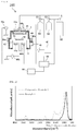
- Fig. 1 is a partial sectional view depicting a configuration of a production device 100 for a silicon nitride film according to the present embodiment.
- This drawing is a schematic view in which peripheral devices including part of a known gas feed mechanism and part of a known exhaust mechanism are not depicted.
- a substrate 20 conveyed by a substrate conveying chamber (not depicted) is mounted on a stage 41 that is provided substantially in the center of a chamber 40.
- the substrate 20 and the interior of the chamber 40 are heated by heaters 44a and 44b provided on an outer wall of the chamber 40.
- the chamber 40 is connected with an organic silane cylinder 50 containing an organic silane gas as one of source gases, via a gas flow regulator 51.
- Typical examples of the organic silane gas according to the present embodiment include tetrakis dimethylamino silane, tris dimethylamino silane, and bis diethylamino silane.
- the chamber 40 is also connected with a gas cylinder 54 containing a hydrogen (H 2 ) gas as an additive gas to be introduced into the chamber 40 along with the organic silane gas according to the present embodiment, via a gas flow regulator 55.
- the chamber 40 is further connected with a gas cylinder 52 containing an ammonia (NH 3 ) gas as an additive gas to be introduced into the chamber 40 in place of or along with hydrogen, via a gas flow regulator 53.
- the chamber 40 includes a shower head gas introducing unit 45.
- the organic silane gas as well as at least one additive gas selected from the group consisting of the hydrogen gas and the ammonia gas are introduced from the shower head gas introducing unit 45 into the chamber 40. Piping from the organic silane cylinder 50 to the chamber 40 is heated by a heater (not depicted) to about 200°C, for example.
- the shower head gas introducing unit 45 is electrically insulated from the chamber 40 by a sealant S in a ring shape.
- the stage 41 is also electrically insulated from the chamber 40 by a sealant S in a ring shape.
- the chamber 40 is also connected, via an exhaust flow regulator 48, with a vacuum pump 47 configured to depressurize the interior of the chamber 40 and discharge a gas to be generated after processing.
- the exhaust flow regulator 48 changes an exhaust flow rate from the chamber 40.
- a controller 49 configured to control the gas flow regulators 51, 53, and 55, the heaters 44a and 44b, power supplies 46a and 46b, and the exhaust flow regulator 48.
- the gases fed from the organic silane cylinder 50, the hydrogen gas cylinder 54, and the ammonia gas cylinder 52 eventually pass through an identical channel to reach the chamber 40.
- the power supply 46a applies electric power of a predetermined frequency to the shower head gas introducing unit 45 to form a plasma of the gases discharged from the shower head gas introducing unit 45.
- the plasma thus generated reaches the substrate 20 on the stage 41 to which the power supply 46b applies electric power of a predetermined frequency as necessary.
- the substrate 20 exposed to the plasma is provided thereon with a silicon nitride film.
- the frequency of the applied electric power is not particularly limited in the present embodiment. At least some of the effects of the present embodiment will be obtained in either case where the frequency is low (e.g. 380 kHz) or high (e.g. 13.56 MHz).
- the production device 100 for a silicon nitride film includes the controller 49 connected to a computer 60.
- the computer 60 monitors or integrally controls a production process for a silicon nitride film in accordance with a production program for a silicon nitride film 30 referred to for execution of the production process.
- the production program according to the present embodiment is stored in a hard disk drive in the computer 60 or a known recording medium such as an optical disk inserted to an optical disk drive provided to the computer 60.
- the production program is not limited in terms of its stored place.
- this production program is partially or entirely stored in the controller 49 included in each processing chamber according to the present embodiment.
- the production process is monitored or controlled in accordance with the production program via a local area network, an internet connection, or the like according to a known technique.
- the production method for the silicon nitride film according to the present embodiment includes the step of forming a plasma of an organic silane and at least one additive gas selected from the group consisting of a hydrogen gas and an ammonia gas by a plasma CVD method to form a silicon nitride film.
- the silicon nitride film according to the present embodiment is made from materials including the organic silane gas by the plasma CVD method.
- typical examples of the organic silane gas according to the present embodiment include tetrakis dimethylamino silane, tris dimethylamino silane, and bis diethylamino silane.
- the substrate 20 to be treated is initially mounted on the stage in the chamber 40.
- the substrate 20 is heated and is subsequently exposed, in the chamber 40, to the organic silane gas and the additive gas thus formed into a plasma by the plasma CVD method.
- a silicon nitride film is formed on the substrate 20.
- the additive gas according to the present embodiment is at least one gas selected from the group consisting of the hydrogen gas and the ammonia gas. These additive gases will contribute to generation of a hydrogen radical to be used for removing carbon atoms or hydrogen atoms in the silicon nitride film in the form of a hydrocarbon gas or a hydrogen gas.
- a leakage current value and/or wet resistance is likely to deteriorate if the silicon nitride film contains many carbon atoms and/or many hydrogen atoms. Accordingly, it is not preferred that the carbon atoms and/or the hydrogen atoms remain in the silicon nitride film.
- a tetrakis dimethylamino silane molecule includes a methyl group. According to a result of theoretical chemical calculation (the Gaussian 09 program, B3LYP/cc-pVDZ) of bond dissociation energy of tetrakis dimethylamino silane by the inventors of the present application, a bond between nitrogen and carbon (N-C bond) is most likely to be dissociated from each other.
- Carbon atoms and/or the hydrogen atoms are thus less likely to be contained in the silicon nitride film.
- the methyl group may further be dissociated and carbon atoms and/or the hydrogen atoms may be contained in the silicon nitride film.
- the present embodiment achieves improvement in properties of the silicon nitride film by introduction of the respective additive gases, which promotes removal of carbon atoms and/or the hydrogen atoms in a reaction system during the formation process of the silicon nitride film in the form of a hydrocarbon gas and/or a hydrogen gas.
- the silicon nitride film is produced under the following specific production conditions in the present embodiment.
- the chamber 40 is fed with the organic silane gas and the additive gas until internal pressure of the chamber 40 reaches a predetermined level.
- the internal pressure of the chamber 40 is preferably 10 Pa or more and 500 Pa or less in terms of a residence time of the materials in the chamber, for allowing the materials to be decomposed in the plasma and react on the substrate.
- the organic silane gas preferably has a flow rate of 0.05 sccm or more and 500 sccm or less in terms of productivity and sufficient decomposition of the materials.
- a mixing ratio between hydrocarbon molecules contained in the organic silane gas and hydrogen atoms contained in the additive gas is preferably in the range from 1 : 1 to 1 : 300 in terms of generation of a hydrocarbon gas and/or a hydrogen gas from carbon atoms and/or hydrogen atoms and its productivity.
- the stage 41 is heated by the heater 44b in the present embodiment until the temperature of the stage 41 reaches a predetermined level.
- the temperature of the stage 41 has an upper limit that is not particularly limited, but is preferably set to 500°C or less in terms of cost efficiency and productivity.
- the temperature of the stage 41 is further preferably set to 400°C or less in terms of the same points. Electric power of the predetermined frequency is subsequently applied to the shower head gas introducing unit 45.
- the silicon nitride film is produced by the above process.
- the silicon nitride film produced at 400°C or less by the production method for the silicon nitride film of the present embodiment has a carbon atom content ratio of less than 0.8 assuming that a sum of a silicon atom content and a nitrogen atom content in the silicon nitride film is 1. Reduction in content ratio of the carbon atoms in the silicon nitride film will highly possibly improve reliability of various devices including the silicon nitride film.
- the silicon nitride film preferably has a carbon atom content ratio of less than 0.4 and more preferably less than 0.2 assuming that a sum of the silicon atom content and the nitrogen atom content in the silicon nitride film is 1.
- the silicon nitride film according to the present embodiment achieves reduction in content by percentage of the hydrogen atoms as well as the carbon atoms.
- the silicon nitride film produced at 400°C or less by the production method for the silicon nitride film according to the present embodiment has a carbon atom content ratio of less than 0.9 assuming that a sum of the silicon atom content and the nitrogen atom content in the silicon nitride film is 1.
- Reduction in content ratio of the hydrogen atoms in the silicon nitride film will highly possibly improve reliability of various devices including the silicon nitride film.
- the silicon nitride film preferably has a hydrogen atom content ratio of less than 0.6 and more preferably less than 0.5 assuming that a sum of the silicon atom content and the nitrogen atom content in the silicon nitride film is 1.
- the silicon nitride film according to the present embodiment achieves a leakage current value of less than 1.0 ⁇ 10 -6 A/cm 2 at a field intensity of 1 MV/cm.
- the silicon nitride film according to the present embodiment will sufficiently serve as an insulating layer.
- the silicon nitride film made from tetrakis dimethylamino silane as the organic silane gas according to the present embodiment achieves a leakage current value of less than 2.6 ⁇ 10 -9 A/cm 2 .
- Elemental analysis was performed in accordance with Rutherford Backscattering spectrometry (RBS spectrometry) and Hydrogen Forward Scattering spectrometry (HFS spectrometry) to obtain atomic composition percentages (at%) of carbon atoms (C), hydrogen atoms (H), silicon atoms (Si), and nitrogen atoms (N) in the silicon nitride film according to each of the examples and the comparative examples.
- RBS spectrometry Rutherford Backscattering spectrometry
- HFS spectrometry Hydrogen Forward Scattering spectrometry
- An infrared absorption spectrum of the silicon nitride film was analyzed.
- the infrared absorption spectrum was measured using a Fourier transform infrared spectrophotometer (FTIR spectrophotometer).
- FTIR spectrophotometer Fourier transform infrared spectrophotometer
- the leakage current value of the silicon nitride film was measured by means of IV measurement using a mercury probe.
- the silicon nitride films according to some of the examples to be mentioned below were analyzed also in terms of wet resistance.
- the wet resistance was evaluated by execution of a pressure cooker test (PCT).
- PCT pressure cooker test
- the PCT was executed at 2 atm and 121°C for 6 hours. This evaluation was made by calculating hygroscopicity from an FTIR spectrum. It is known that a Si-N bond is replaced with a Si-O bond when a silicon nitride film absorbs moisture. The evaluation was thus made based on a numerical value obtained by subtracting Si-N absorption intensity from Si-O absorption intensity. Accordingly, a smaller numerical value indicates higher wet resistance.
- a silicon nitride film according to Example 1 was produced by the production method of the first embodiment. Tetrakis dimethylamino silane was used as the organic silane gas as one of the materials and a hydrogen gas was used as the additive gas.
- the internal pressure of the chamber 40 was set to 93.3 Pa, and 1 sccm of tetrakis dimethylamino silane and 400 sccm of the hydrogen gas were fed. Electric power of 13.56 MHz and 600 W was applied to the shower head gas introducing unit 45.
- the temperature of the stage was set to 300°C.
- a silicon nitride film was produced under conditions similar to those of Example 1 except that a hydrogen gas and an ammonia gas were used as the additive gases as source gases, and were fed at flow rates of 300 sccm and 100 sccm, respectively.
- a silicon nitride film was produced under conditions similar to those of Example 1 except that an ammonia gas was used as the additive gas as a source gas, and was fed at a flow rate of 400 sccm.
- a silicon nitride film was produced under conditions similar to those of Example 1 except that tris dimethylamino silane was used as the organic silane gas as a source gas, and was fed at a flow rate of 1 sccm.
- a silicon nitride film was produced under conditions similar to those of Example 2 except that tris dimethylamino silane was used as the organic silane gas, and was fed at a flow rate of 1 sccm.
- a silicon nitride film was produced under conditions similar to those of Example 3 except that tris dimethylamino silane was used as the organic silane gas, and was fed at a flow rate of 1 sccm.
- a silicon nitride film was produced under conditions similar to those of Example 1 except that bis diethylamino silane was used as the organic silane gas as a source gas, and was fed at a flow rate of 1 sccm.
- a silicon nitride film was produced under conditions similar to those of Example 2 except that bis diethylamino silane was used as the organic silane gas as a source gas, and was fed at a flow rate of 1 sccm.
- a silicon nitride film was produced under conditions similar to those of Example 3 except that bis diethylamino silane was used as the organic silane gas as a source gas, and was fed at a flow rate of 1 sccm.
- a silicon nitride film according to Comparative Example 1 was produced under conditions similar to those of Example 1 except that a helium gas was used as a diluent gas incapable of providing any hydrogen radical, and was fed at a flow rate of 400 sccm.
- a silicon nitride film according to Comparative Example 2 was produced under conditions similar to those of Example 4 except that a helium gas was used as a diluent gas incapable of providing any hydrogen radical, and was fed at a flow rate of 400 sccm.
- a silicon nitride film according to Comparative Example 3 was produced under conditions similar to those of Example 7 except that a helium gas was used as a diluent gas incapable of providing any hydrogen radical, and was fed at a flow rate of 400 sccm.
- Example 1 One of source gases (Organic silane gas) Composition ratio/ measurement target
- Example 2 Example 3 Comparative Example 1 Tetrakis diethylamino silane (4DMAS) C/(Si+N) 0.18 0.14 0.13 0.91 H/CSi+N) 0.44 0.44 0.48 0.94 Leakage current (A/cm 2 ) 4.77E-09 2.87E-09 2.56E-09 2.72E-06 Wet resistance evaluation 0.002 0.003 0.003 0.08 Tris diethylamino silane (3DMAS) Composition ratio/ measurement target
- Example 5 Example 6 Comparative Example 2 C/(Si+N) 0.19 0.14 0.13 0.86 H/CSi+N) 0.42 0.44 0.48 0.92 Leakage current (A/cm 2 ) 2.67E-09 2.38E-09 2.11E-09 5.66E-06 Wet resistance evaluation 0.002 0.003 0.002 0.05 Bis dimethylamino silane (BDEAS) Composition ratio/ measurement target
- the carbon atom content ratio is less than 0.8 assuming that a sum of the silicon atom content and the nitrogen atom content is 1 in the silicon nitride film according to each of Examples 1 to 9 in which tetrakis dimethylamino silane, tris dimethylamino silane, or bis diethylamino silane was used as one of the source gases.
- the silicon nitride film has a carbon atom content ratio of 0.13 or more and 0.19 or less assuming that a sum of the silicon atom content and the nitrogen atom content is 1 in the silicon nitride film produced using tetrakis dimethylamino silane or tris dimethylamino silane as the organic silane gas according to the present embodiment.
- the silicon nitride film was found to have a carbon atom content ratio of 0.8 or more assuming that a sum of the silicon atom content and the nitrogen atom content in the silicon nitride film is 1.
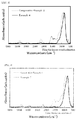
- Figs. 2 to 4 indicate absorbance spectra according to Examples 1, 4, and 7 as well as Comparative Examples 1 to 3 as representative examples.
- Figs. 2 to 4 indicate peaks at about a wavenumber of 850 cm -1 due to Si-N stretching vibration absorption, peaks at about a wavenumber of 2180 cm -1 due to Si-H stretching vibration absorption, peaks at about a wavenumber of 2950 cm -1 due to C-H stretching vibration absorption, and peaks at about a wavenumber of 3380 cm -1 due to N-H stretching vibration absorption. Peak intensity ratios of Si-H, C-H, and N-H to Si-N peak intensity are shown in Table 2.
- the leakage current value at a field intensity of 1 MV/cm according to each of the examples was less than 1.0 ⁇ 10 -6 A/cm 2 . It was found that the leakage current decreases as a result of a decrease in the carbon atom content ratio and/or the hydrogen atom content ratio assuming that a sum of the silicon atom content and the nitrogen atom content is 1, in comparison to that according to each of the comparative examples.
- the measurement results according to each of the examples indicate that a preferred leakage current value and good wet resistance are achieved when the carbon atom content ratio and/or the hydrogen atom content ratio is decreased significantly assuming that a sum the silicon atom content and the nitrogen atom content in the silicon nitride film is 1.
- the silicon nitride film according to the embodiment described above thus achieves reduced leakage current as well as higher wet resistance since the carbon atom content ratio is small assuming that a sum of at least the silicon atom content and the nitrogen atom content in the silicon nitride film is 1. Furthermore, in the silicon nitride film according to the embodiment described above, reduction in hydrogen atom content ratio is achieved assuming that a sum of the silicon atom content and the nitrogen atom content in the silicon nitride film is 1. Thus, it is made possible to suppress or prevent temporal variation in quality of the silicon nitride film.
- the hydrogen gas and/or the ammonia gas is used as an additive gas in the above embodiment.
- a deuterium gas is used as a different additive gas in place of or along with the hydrogen gas.
- the above embodiment adopts a plasma generator configured to generate a parallel-plate capacitive-coupled plasma (CCP), but the present invention is not limited thereto.
- a plasma generator configured to generate a different high-density plasma such as an inductively-coupled plasma (ICP) or an electron-cyclotron resonance plasma (ECR).
- ICP inductively-coupled plasma
- ECR electron-cyclotron resonance plasma
Landscapes
- Chemical & Material Sciences (AREA)
- Engineering & Computer Science (AREA)
- Plasma & Fusion (AREA)
- Physics & Mathematics (AREA)
- Organic Chemistry (AREA)
- Analytical Chemistry (AREA)
- Materials Engineering (AREA)
- Mechanical Engineering (AREA)
- Metallurgy (AREA)
- Chemical Kinetics & Catalysis (AREA)
- General Chemical & Material Sciences (AREA)
- Inorganic Chemistry (AREA)
- Life Sciences & Earth Sciences (AREA)
- Wood Science & Technology (AREA)
- Formation Of Insulating Films (AREA)
- Chemical Vapour Deposition (AREA)
Abstract
Description
- The present invention relates to a silicon nitride film made of an organic silane material, a production method therefor, and a production device therefor.
- Various devices including a semiconductor have been developed and many techniques for film formation and film processing have been disclosed to date. There has been disclosed a silicon carbonitride film according to a conventional technique, which was devised in order to solve the problem that a carbon nitride film has an unstable and small nitrogen content. There has also been disclosed an example of forming a silicon carbonitride film by a plasma CVD method using tetrakis dimethylamino silane as a material (Patent Document 1).
- Patent Document 1:
Japanese Patent Laid-open Publication No. 2011-89186 - In the production of a silicon nitride film by a plasma CVD method, an inorganic silane that has high explosibility is used. Use of an organic silane having low explosibility as a material is significant in terms of safety. However, as disclosed in
Patent Document 1, a silicon nitride film formed by the plasma CVD method using an organic silane such as tetrakis dimethylamino silane as a material contains hydrocarbon groups, so that the silicon nitride film has quite a high carbon atom content (e.g. a carbon atom content ratio of 1.86 assuming that a sum of a silicon atom content and a nitrogen atom content is 1). In a silicon nitride film containing many carbon atoms and many hydrogen atoms, many C-C bonds, N-C bonds, or Si-H bonds are formed. These bonds highly possibly cause increase in leakage current and/or deterioration in wet resistance. Further improvement in properties (particularly electrical properties or wet resistance) of a silicon nitride film is thus required for improvement in reliability of various devices including the silicon nitride film. - The present invention has been devised to achieve the object mentioned above, improves various properties of a silicon nitride film, which is formed by a plasma CVD method using an organic silane as a material, and significantly contributes to improvement in reliability of various devices including the silicon nitride film.
- The inventors of the present application have found that improvement in electrical property or wet resistance is quite difficult if the techniques as well as the technique according to
Patent Document 1 for formation of a silicon nitride film using, as a material, the already disclosed organic silane, particularly due to a large carbon atom content ratio and/or a large hydrogen atom content ratio. The inventors have gone through intensive researches and repeated trial and error for solving the problems. The inventors have finally found that use of at least one particular additive gas as one of source gases along with an organic silane such as tetrakis dimethylamino silane achieves reduction in carbon atom content and/or hydrogen atom content in the silicon nitride film as well as improvement in properties of the silicon nitride film including wet resistance or electrical properties represented by leakage current. A silicon nitride film, a production method for the silicon nitride film, and a production device for the silicon nitride film according to the present invention have been devised in view of the above points. - The present invention provides an exemplary silicon nitride film formed by a plasma CVD method using an organic silane as one of materials. The silicon nitride film has a carbon atom content ratio of less than 0.8 assuming that a sum of a silicon atom content and a nitrogen atom content in the silicon nitride film is 1.
- The silicon nitride film has a small carbon atom content ratio and/or a small hydrogen atom content ratio assuming that a sum of the silicon atom content and the nitrogen atom content is 1, even in the case where the organic silane is used as one of source gases. Accordingly, the silicon nitride film achieves a low leakage current value and/or high wet resistance, for example. It is thus possible to improve reliability of various devices including the silicon nitride film.
- An exemplary production method for a silicon nitride film according to the present invention includes the step of forming a plasma of an organic silane and at least one additive gas selected from the group consisting of a hydrogen gas and an ammonia gas by a plasma CVD method to form a silicon nitride film.
- The production method for the silicon nitride film achieves reduction in carbon atom content ratio and/or hydrogen atom content ratio assuming that a sum of a silicon atom content and a nitrogen atom content is 1, even in the case where the organic silane is used as one of source gases. This production method will achieve a low leakage current value and/or high wet resistance, for example, and will thus enable improvement in reliability of various devices including the silicon nitride film.
- The present invention provides an exemplary production device for a silicon nitride film, and the device includes a gas introducing unit configured to introduce into a chamber an organic silane and at least one additive gas selected from the group consisting of a hydrogen gas and an ammonia gas, and a plasma generator configured to form a plasma of the organic silane and the additive gas in the chamber.
- The production device for the silicon nitride film achieves production of a silicon nitride film having a reduced carbon atom content ratio and/or a reduced hydrogen atom content ratio assuming that a sum of a silicon atom content and a nitrogen atom content is 1, even in the case where the organic silane is used as one of source gases. Accordingly, this production device will achieve production of the silicon nitride film having a low leakage current value and/or high wet resistance, for example.
- The exemplary silicon nitride film according to the present invention achieves a low leakage current value and/or high wet resistance, for example, even in the case where the organic silane is used as one of the source gases.
- The exemplary production method for the silicon nitride film according to the present invention achieves reduction in carbon atom content ratio and/or hydrogen atom content ratio assuming that a sum of the silicon atom content and the nitrogen atom content in the silicon nitride film is 1, even in the case where the organic silane is used as one of the source gases.
- The exemplary production device for the silicon nitride film according to the present invention achieves production of the silicon nitride film having a reduced carbon atom content ratio and/or a reduced hydrogen atom content ratio assuming that a sum of the silicon atom content and the nitrogen atom content in the silicon nitride film is 1, even in the case where the organic silane is used as one of the source gases.
-
-
Fig. 1 is a partial sectional view depicting a configuration of a production device for a silicon nitride film according to an embodiment of the present invention. -
Fig. 2 is a graph indicating measurement results of infrared absorption spectra of silicon nitride films according to Example 1 and Comparative Example 1. -
Fig. 3 is a graph indicating measurement results of infrared absorption spectra of silicon nitride films according to Example 4 and Comparative Example 2. -
Fig. 4 is a graph indicating measurement results of infrared absorption spectra of silicon nitride films according to Example 7 and Comparative Example 3. - An embodiment of the present invention will now be described in detail with reference to the accompanying drawings. Common parts will be denoted by common reference signs throughout all the drawings in this description. Elements according to the present embodiment will not always be depicted at relative scale ratios in the drawings. Flow rates of various gases to be indicated below will be under a standard condition.
-
Fig. 1 is a partial sectional view depicting a configuration of aproduction device 100 for a silicon nitride film according to the present embodiment. This drawing is a schematic view in which peripheral devices including part of a known gas feed mechanism and part of a known exhaust mechanism are not depicted. - A
substrate 20 conveyed by a substrate conveying chamber (not depicted) is mounted on astage 41 that is provided substantially in the center of achamber 40. Thesubstrate 20 and the interior of thechamber 40 are heated byheaters chamber 40. Thechamber 40 is connected with anorganic silane cylinder 50 containing an organic silane gas as one of source gases, via agas flow regulator 51. Typical examples of the organic silane gas according to the present embodiment include tetrakis dimethylamino silane, tris dimethylamino silane, and bis diethylamino silane. - The
chamber 40 is also connected with agas cylinder 54 containing a hydrogen (H2) gas as an additive gas to be introduced into thechamber 40 along with the organic silane gas according to the present embodiment, via agas flow regulator 55. Thechamber 40 is further connected with agas cylinder 52 containing an ammonia (NH3) gas as an additive gas to be introduced into thechamber 40 in place of or along with hydrogen, via agas flow regulator 53. Thechamber 40 includes a shower headgas introducing unit 45. - According to the present embodiment, the organic silane gas as well as at least one additive gas selected from the group consisting of the hydrogen gas and the ammonia gas are introduced from the shower head
gas introducing unit 45 into thechamber 40. Piping from theorganic silane cylinder 50 to thechamber 40 is heated by a heater (not depicted) to about 200°C, for example. - The shower head
gas introducing unit 45 is electrically insulated from thechamber 40 by a sealant S in a ring shape. Thestage 41 is also electrically insulated from thechamber 40 by a sealant S in a ring shape. Thechamber 40 is also connected, via anexhaust flow regulator 48, with avacuum pump 47 configured to depressurize the interior of thechamber 40 and discharge a gas to be generated after processing. Theexhaust flow regulator 48 changes an exhaust flow rate from thechamber 40. There is provided acontroller 49 configured to control thegas flow regulators heaters power supplies exhaust flow regulator 48. - The gases fed from the
organic silane cylinder 50, thehydrogen gas cylinder 54, and theammonia gas cylinder 52 eventually pass through an identical channel to reach thechamber 40. Thepower supply 46a applies electric power of a predetermined frequency to the shower headgas introducing unit 45 to form a plasma of the gases discharged from the shower headgas introducing unit 45. The plasma thus generated reaches thesubstrate 20 on thestage 41 to which thepower supply 46b applies electric power of a predetermined frequency as necessary. Thesubstrate 20 exposed to the plasma is provided thereon with a silicon nitride film. The frequency of the applied electric power is not particularly limited in the present embodiment. At least some of the effects of the present embodiment will be obtained in either case where the frequency is low (e.g. 380 kHz) or high (e.g. 13.56 MHz). - The
production device 100 for a silicon nitride film according to the present embodiment includes thecontroller 49 connected to acomputer 60. Thecomputer 60 monitors or integrally controls a production process for a silicon nitride film in accordance with a production program for asilicon nitride film 30 referred to for execution of the production process. The production program according to the present embodiment is stored in a hard disk drive in thecomputer 60 or a known recording medium such as an optical disk inserted to an optical disk drive provided to thecomputer 60. The production program is not limited in terms of its stored place. Alternatively, this production program is partially or entirely stored in thecontroller 49 included in each processing chamber according to the present embodiment. Still alternatively, the production process is monitored or controlled in accordance with the production program via a local area network, an internet connection, or the like according to a known technique. - A production method for a silicon nitride film will be described next. The production method for the silicon nitride film according to the present embodiment includes the step of forming a plasma of an organic silane and at least one additive gas selected from the group consisting of a hydrogen gas and an ammonia gas by a plasma CVD method to form a silicon nitride film.
- The silicon nitride film according to the present embodiment is made from materials including the organic silane gas by the plasma CVD method. As described above, typical examples of the organic silane gas according to the present embodiment include tetrakis dimethylamino silane, tris dimethylamino silane, and bis diethylamino silane.
- According to the present embodiment, the
substrate 20 to be treated is initially mounted on the stage in thechamber 40. Thesubstrate 20 is heated and is subsequently exposed, in thechamber 40, to the organic silane gas and the additive gas thus formed into a plasma by the plasma CVD method. As a result, a silicon nitride film is formed on thesubstrate 20. The additive gas according to the present embodiment is at least one gas selected from the group consisting of the hydrogen gas and the ammonia gas. These additive gases will contribute to generation of a hydrogen radical to be used for removing carbon atoms or hydrogen atoms in the silicon nitride film in the form of a hydrocarbon gas or a hydrogen gas. - A leakage current value and/or wet resistance is likely to deteriorate if the silicon nitride film contains many carbon atoms and/or many hydrogen atoms. Accordingly, it is not preferred that the carbon atoms and/or the hydrogen atoms remain in the silicon nitride film. For example, a tetrakis dimethylamino silane molecule includes a methyl group. According to a result of theoretical chemical calculation (the Gaussian 09 program, B3LYP/cc-pVDZ) of bond dissociation energy of tetrakis dimethylamino silane by the inventors of the present application, a bond between nitrogen and carbon (N-C bond) is most likely to be dissociated from each other. Carbon atoms and/or the hydrogen atoms are thus less likely to be contained in the silicon nitride film. However, the methyl group may further be dissociated and carbon atoms and/or the hydrogen atoms may be contained in the silicon nitride film. In view of this, the present embodiment achieves improvement in properties of the silicon nitride film by introduction of the respective additive gases, which promotes removal of carbon atoms and/or the hydrogen atoms in a reaction system during the formation process of the silicon nitride film in the form of a hydrocarbon gas and/or a hydrogen gas.
- The silicon nitride film is produced under the following specific production conditions in the present embodiment. First, the
chamber 40 is fed with the organic silane gas and the additive gas until internal pressure of thechamber 40 reaches a predetermined level. The internal pressure of thechamber 40 is preferably 10 Pa or more and 500 Pa or less in terms of a residence time of the materials in the chamber, for allowing the materials to be decomposed in the plasma and react on the substrate. The organic silane gas preferably has a flow rate of 0.05 sccm or more and 500 sccm or less in terms of productivity and sufficient decomposition of the materials. Furthermore, a mixing ratio between hydrocarbon molecules contained in the organic silane gas and hydrogen atoms contained in the additive gas is preferably in the range from 1 : 1 to 1 : 300 in terms of generation of a hydrocarbon gas and/or a hydrogen gas from carbon atoms and/or hydrogen atoms and its productivity. - The
stage 41 is heated by theheater 44b in the present embodiment until the temperature of thestage 41 reaches a predetermined level. The temperature of thestage 41 has an upper limit that is not particularly limited, but is preferably set to 500°C or less in terms of cost efficiency and productivity. The temperature of thestage 41 is further preferably set to 400°C or less in terms of the same points. Electric power of the predetermined frequency is subsequently applied to the shower headgas introducing unit 45. - The silicon nitride film is produced by the above process. The silicon nitride film produced at 400°C or less by the production method for the silicon nitride film of the present embodiment has a carbon atom content ratio of less than 0.8 assuming that a sum of a silicon atom content and a nitrogen atom content in the silicon nitride film is 1. Reduction in content ratio of the carbon atoms in the silicon nitride film will highly possibly improve reliability of various devices including the silicon nitride film. In terms of the above points, the silicon nitride film preferably has a carbon atom content ratio of less than 0.4 and more preferably less than 0.2 assuming that a sum of the silicon atom content and the nitrogen atom content in the silicon nitride film is 1.
- The silicon nitride film according to the present embodiment achieves reduction in content by percentage of the hydrogen atoms as well as the carbon atoms. Specifically, the silicon nitride film produced at 400°C or less by the production method for the silicon nitride film according to the present embodiment has a carbon atom content ratio of less than 0.9 assuming that a sum of the silicon atom content and the nitrogen atom content in the silicon nitride film is 1. Reduction in content ratio of the hydrogen atoms in the silicon nitride film will highly possibly improve reliability of various devices including the silicon nitride film. In terms of the above points, the silicon nitride film preferably has a hydrogen atom content ratio of less than 0.6 and more preferably less than 0.5 assuming that a sum of the silicon atom content and the nitrogen atom content in the silicon nitride film is 1.
- The silicon nitride film according to the present embodiment achieves a leakage current value of less than 1.0 × 10⁻⁶ A/cm2 at a field intensity of 1 MV/cm. When the leakage current value at a field intensity of 1 MV/cm is less than 1.0 × 10⁻⁸ A/cm2, the silicon nitride film according to the present embodiment will sufficiently serve as an insulating layer. As to be described later, it is worth mentioning that the silicon nitride film made from tetrakis dimethylamino silane as the organic silane gas according to the present embodiment achieves a leakage current value of less than 2.6 × 10⁻⁹ A/cm2.
- Examples and comparative examples will be described below, but the present invention is not limited to these examples. In each of the examples and the comparative examples, physical properties of the silicon nitride film were measured and composition of the silicon nitride film was analyzed by the following methods.
- Elemental analysis was performed in accordance with Rutherford Backscattering spectrometry (RBS spectrometry) and Hydrogen Forward Scattering spectrometry (HFS spectrometry) to obtain atomic composition percentages (at%) of carbon atoms (C), hydrogen atoms (H), silicon atoms (Si), and nitrogen atoms (N) in the silicon nitride film according to each of the examples and the comparative examples.
- An infrared absorption spectrum of the silicon nitride film was analyzed. The infrared absorption spectrum was measured using a Fourier transform infrared spectrophotometer (FTIR spectrophotometer).
- The leakage current value of the silicon nitride film was measured by means of IV measurement using a mercury probe.
- The silicon nitride films according to some of the examples to be mentioned below were analyzed also in terms of wet resistance. The wet resistance was evaluated by execution of a pressure cooker test (PCT). The PCT was executed at 2 atm and 121°C for 6 hours. This evaluation was made by calculating hygroscopicity from an FTIR spectrum. It is known that a Si-N bond is replaced with a Si-O bond when a silicon nitride film absorbs moisture. The evaluation was thus made based on a numerical value obtained by subtracting Si-N absorption intensity from Si-O absorption intensity. Accordingly, a smaller numerical value indicates higher wet resistance.
- A silicon nitride film according to Example 1 was produced by the production method of the first embodiment. Tetrakis dimethylamino silane was used as the organic silane gas as one of the materials and a hydrogen gas was used as the additive gas. The internal pressure of the
chamber 40 was set to 93.3 Pa, and 1 sccm of tetrakis dimethylamino silane and 400 sccm of the hydrogen gas were fed. Electric power of 13.56 MHz and 600 W was applied to the shower headgas introducing unit 45. The temperature of the stage was set to 300°C. - A silicon nitride film was produced under conditions similar to those of Example 1 except that a hydrogen gas and an ammonia gas were used as the additive gases as source gases, and were fed at flow rates of 300 sccm and 100 sccm, respectively.
- A silicon nitride film was produced under conditions similar to those of Example 1 except that an ammonia gas was used as the additive gas as a source gas, and was fed at a flow rate of 400 sccm.
- A silicon nitride film was produced under conditions similar to those of Example 1 except that tris dimethylamino silane was used as the organic silane gas as a source gas, and was fed at a flow rate of 1 sccm.
- A silicon nitride film was produced under conditions similar to those of Example 2 except that tris dimethylamino silane was used as the organic silane gas, and was fed at a flow rate of 1 sccm.
- A silicon nitride film was produced under conditions similar to those of Example 3 except that tris dimethylamino silane was used as the organic silane gas, and was fed at a flow rate of 1 sccm.
- A silicon nitride film was produced under conditions similar to those of Example 1 except that bis diethylamino silane was used as the organic silane gas as a source gas, and was fed at a flow rate of 1 sccm.
- A silicon nitride film was produced under conditions similar to those of Example 2 except that bis diethylamino silane was used as the organic silane gas as a source gas, and was fed at a flow rate of 1 sccm.
- A silicon nitride film was produced under conditions similar to those of Example 3 except that bis diethylamino silane was used as the organic silane gas as a source gas, and was fed at a flow rate of 1 sccm.
- A silicon nitride film according to Comparative Example 1 was produced under conditions similar to those of Example 1 except that a helium gas was used as a diluent gas incapable of providing any hydrogen radical, and was fed at a flow rate of 400 sccm.
- A silicon nitride film according to Comparative Example 2 was produced under conditions similar to those of Example 4 except that a helium gas was used as a diluent gas incapable of providing any hydrogen radical, and was fed at a flow rate of 400 sccm.
- A silicon nitride film according to Comparative Example 3 was produced under conditions similar to those of Example 7 except that a helium gas was used as a diluent gas incapable of providing any hydrogen radical, and was fed at a flow rate of 400 sccm.
- Carbon atom content ratios and hydrogen atom content ratios assuming that a sum of a silicon atom content and a nitrogen atom content obtained from the contents by percentage of the elements in the silicon nitride film according to each of Examples 1 to 9 and Comparative Examples 1 to 3 is 1, as well as electrical properties and evaluation results of wet resistance of the silicon nitride films are shown in Table 1.
Table 1 One of source gases (Organic silane gas) Composition ratio/ measurement target Example 1 Example 2 Example 3 Comparative Example 1 Tetrakis diethylamino silane (4DMAS) C/(Si+N) 0.18 0.14 0.13 0.91 H/CSi+N) 0.44 0.44 0.48 0.94 Leakage current (A/cm2) 4.77E-09 2.87E-09 2.56E-09 2.72E-06 Wet resistance evaluation 0.002 0.003 0.003 0.08 Tris diethylamino silane (3DMAS) Composition ratio/ measurement target Example 4 Example 5 Example 6 Comparative Example 2 C/(Si+N) 0.19 0.14 0.13 0.86 H/CSi+N) 0.42 0.44 0.48 0.92 Leakage current (A/cm2) 2.67E-09 2.38E-09 2.11E-09 5.66E-06 Wet resistance evaluation 0.002 0.003 0.002 0.05 Bis dimethylamino silane (BDEAS) Composition ratio/ measurement target Example 7 Example 8 Example 9 Comparative Example 3 C/(Si+N) 0.38 0.31 0.28 0.94 H/CSi+N) 0.51 0.54 0.57 0.91 Leakage current (A/cm2) 8.55E-07 6.78E-07 5.22E-07 5.20E-06 Wet resistance evaluation 0.002 0.004 0.003 0.04 - It is a preferred aspect in terms of more reliable achievement of the effects of the silicon nitride film according to the first embodiment that the carbon atom content ratio is less than 0.8 assuming that a sum of the silicon atom content and the nitrogen atom content is 1 in the silicon nitride film according to each of Examples 1 to 9 in which tetrakis dimethylamino silane, tris dimethylamino silane, or bis diethylamino silane was used as one of the source gases. It is worth mentioning that the silicon nitride film has a carbon atom content ratio of 0.13 or more and 0.19 or less assuming that a sum of the silicon atom content and the nitrogen atom content is 1 in the silicon nitride film produced using tetrakis dimethylamino silane or tris dimethylamino silane as the organic silane gas according to the present embodiment.
- In Comparative Examples 1 to 3, the silicon nitride film was found to have a carbon atom content ratio of 0.8 or more assuming that a sum of the silicon atom content and the nitrogen atom content in the silicon nitride film is 1.
-
Figs. 2 to 4 indicate absorbance spectra according to Examples 1, 4, and 7 as well as Comparative Examples 1 to 3 as representative examples.Figs. 2 to 4 indicate peaks at about a wavenumber of 850 cm-1 due to Si-N stretching vibration absorption, peaks at about a wavenumber of 2180 cm-1 due to Si-H stretching vibration absorption, peaks at about a wavenumber of 2950 cm-1 due to C-H stretching vibration absorption, and peaks at about a wavenumber of 3380 cm-1 due to N-H stretching vibration absorption. Peak intensity ratios of Si-H, C-H, and N-H to Si-N peak intensity are shown in Table 2. In comparison to Comparative Examples 1 to 3 in which no additive gas was used, Examples 1, 4, and 7 had less absorption of the carbon atoms and the hydrogen atoms. It is thus found that use of an additive gas leads to reduction in carbon atom content.Table 2 One of source gases (Organic silane gas) Intensity ratio/ measurement target Example 1 Comparative Example 1 Tetrakis dimethylamino silane (4DMAS) Si-H/Si-N 0.0234 0.13259 N-H/Si-N 0.0254 0.10367 C-H/Si-N 0.0183 0.01833 Tris dimethylamino silane (3DMAS) Intensity ratio/ measurement target Example 4 Comparative Example 2 Si-H/Si-N 0.0303 0.1451 N-H/Si-N 0.0282 0.0743 C-H/Si-N 0.0161 0.0268 Bis dimethylamino silane (BDEAS) Intensity ratio/ measurement target Example 7 Comparative Example 3 Si-H/Si-N 0.0376 0.0821 N-H/Si-N 0.0148 0.0750 C-H/Si-N 0.0188 0.0544 - The leakage current value at a field intensity of 1 MV/cm according to each of the examples was less than 1.0 × 10⁻⁶ A/cm2. It was found that the leakage current decreases as a result of a decrease in the carbon atom content ratio and/or the hydrogen atom content ratio assuming that a sum of the silicon atom content and the nitrogen atom content is 1, in comparison to that according to each of the comparative examples.
-
- (4) The wet resistance evaluated in each of the examples was less than 0.04. It was found that the wet resistance improves as a result of a decrease in the carbon atom content ratio and/or the hydrogen atom content ratio assuming that a sum of the silicon atom content and the nitrogen atom content is 1, in comparison to that according to each of the comparative examples.
- The measurement results according to each of the examples indicate that a preferred leakage current value and good wet resistance are achieved when the carbon atom content ratio and/or the hydrogen atom content ratio is decreased significantly assuming that a sum the silicon atom content and the nitrogen atom content in the silicon nitride film is 1.
- The silicon nitride film according to the embodiment described above thus achieves reduced leakage current as well as higher wet resistance since the carbon atom content ratio is small assuming that a sum of at least the silicon atom content and the nitrogen atom content in the silicon nitride film is 1. Furthermore, in the silicon nitride film according to the embodiment described above, reduction in hydrogen atom content ratio is achieved assuming that a sum of the silicon atom content and the nitrogen atom content in the silicon nitride film is 1. Thus, it is made possible to suppress or prevent temporal variation in quality of the silicon nitride film. Application of the silicon nitride film according to the above embodiment achieving improvement in insulation and wet resistance as an insulating film, a dielectric film, a passivation film, or the like of various electronic devices significantly contributes to improvement in reliability and/or properties of these devices.
- The hydrogen gas and/or the ammonia gas is used as an additive gas in the above embodiment. According to another adoptable aspect, a deuterium gas is used as a different additive gas in place of or along with the hydrogen gas.
- The above embodiment adopts a plasma generator configured to generate a parallel-plate capacitive-coupled plasma (CCP), but the present invention is not limited thereto. The effects of the present invention will also be achieved by alternatively using a plasma generator configured to generate a different high-density plasma such as an inductively-coupled plasma (ICP) or an electron-cyclotron resonance plasma (ECR).
- The above embodiments have been disclosed for description of these embodiments and not for limitation to the present invention. Any modification example within the scope of the present invention, inclusive of other combinations of the embodiments, will also be included within the scope of patent claims.
-
- 20
- Substrate
- 30, 130
- Silicon nitride film
- 41
- Stage
- 50, 52, 54
- Gas cylinder
- 50
- Organic silane cylinder
- 51, 53, 55
- Gas flow regulator
- 40
- Chamber
- 46a, 46b
- Power supply
- 47
- Vacuum pump
- 48
- Exhaust flow regulator
- 49
- Controller
- 44a, 44b
- Heater
- 45
- Shower head gas introducing unit
- 100
- Production device for silicon nitride film
Claims (13)
- A silicon nitride film formed by a plasma CVD method using an organic silane as one of materials, wherein the silicon nitride film has a carbon atom content ratio of less than 0.8 assuming that a sum of a silicon atom content and a nitrogen atom content in the silicon nitride film is 1.
- The silicon nitride film according to claim 1, wherein the silicon nitride film has a hydrogen atom content ratio of less than 0.9 assuming that a sum of the silicon atom content and the nitrogen atom content in the silicon nitride film is 1.
- The silicon nitride film according to claim 1 or 2, having a leakage current value of less than 1.0 × 10⁻⁶ A/cm2 at a field intensity of 1 MV/cm.
- The silicon nitride film according to any one of claims 1 to 3, wherein the organic silane is tetrakis dimethylamino silane, tris dimethylamino silane, or bis diethylamino silane.
- A device comprising the silicon nitride film according to any one of claims 1 to 4 as an insulating film, a dielectric film, or a passivation film.
- A production method for a silicon nitride film, the method comprising:forming a plasma of an organic silane and at least one additive gas selected from the group consisting of a hydrogen gas and an ammonia gas by a plasma CVD method to form a silicon nitride film.
- The production method for the silicon nitride film according to claim 6, wherein the silicon nitride film has a carbon atom content ratio of less than 0.8 assuming that a sum of a silicon atom content and a nitrogen atom content in the silicon nitride film is 1.
- The production method for the silicon nitride film according to claim 6 or 7, wherein the silicon nitride film has a hydrogen atom content ratio of less than 0.9 assuming that a sum of a silicon atom content and a nitrogen atom content in the silicon nitride film is 1.
- The production method for the silicon nitride film according to any one of claims 6 to 8, wherein the organic silane is tetrakis dimethylamino silane, tris dimethylamino silane, or bis diethylamino silane.
- A production device for a silicon nitride film, the device comprising:a gas introducing unit configured to introduce into a chamber an organic silane and at least one additive gas selected from the group consisting of a hydrogen gas and an ammonia gas, and a plasma generator configured to form a plasma of the organic silane and the additive gas in the chamber.
- The production device for the silicon nitride film according to claim 10, configured to form, on a treatment target mounted on a stage provided in the chamber, a silicon nitride film having a carbon atom content ratio of less than 0.8 assuming that a sum of a silicon atom content and a nitrogen atom content in the silicon nitride film is 1.
- The production device for the silicon nitride film according to claim 10 or 11, configured to form, on a treatment target mounted on a stage provided in the chamber, a silicon nitride film having a hydrogen atom content ratio of less than 0.9 assuming that a sum of a silicon atom content and a nitrogen atom content in the silicon nitride film is 1.
- The production device for the silicon nitride film according to any one of claims 10 to 12, wherein the organic silane is tetrakis dimethylamino silane, tris dimethylamino silane, or bis diethylamino silane.
Applications Claiming Priority (2)
| Application Number | Priority Date | Filing Date | Title |
|---|---|---|---|
| JP2013246798 | 2013-11-28 | ||
| PCT/JP2014/080300 WO2015079938A1 (en) | 2013-11-28 | 2014-11-17 | Silicon nitride film, production method therefor, and production device therefor |
Publications (2)
| Publication Number | Publication Date |
|---|---|
| EP3076423A1 true EP3076423A1 (en) | 2016-10-05 |
| EP3076423A4 EP3076423A4 (en) | 2017-11-01 |
Family
ID=53198884
Family Applications (1)
| Application Number | Title | Priority Date | Filing Date |
|---|---|---|---|
| EP14866390.9A Withdrawn EP3076423A4 (en) | 2013-11-28 | 2014-11-17 | Silicon nitride film, production method therefor, and production device therefor |
Country Status (7)
| Country | Link |
|---|---|
| US (1) | US10280084B2 (en) |
| EP (1) | EP3076423A4 (en) |
| JP (1) | JPWO2015079938A1 (en) |
| KR (1) | KR102128589B1 (en) |
| CN (1) | CN105765705B (en) |
| TW (1) | TWI646600B (en) |
| WO (1) | WO2015079938A1 (en) |
Families Citing this family (3)
| Publication number | Priority date | Publication date | Assignee | Title |
|---|---|---|---|---|
| US10559459B2 (en) | 2016-03-11 | 2020-02-11 | Taiyo Nippon Sanso Corporation | Method for producing silicon nitride film and silicon nitride film |
| JP6652644B2 (en) * | 2016-07-21 | 2020-02-26 | 株式会社Kokusai Electric | Plasma generation apparatus, substrate processing apparatus, semiconductor device manufacturing method and program |
| US10950428B1 (en) * | 2019-08-30 | 2021-03-16 | Mattson Technology, Inc. | Method for processing a workpiece |
Family Cites Families (11)
| Publication number | Priority date | Publication date | Assignee | Title |
|---|---|---|---|---|
| JP2637265B2 (en) * | 1990-06-28 | 1997-08-06 | 株式会社東芝 | Method of forming silicon nitride film |
| JPH06132284A (en) * | 1992-10-22 | 1994-05-13 | Kawasaki Steel Corp | Method for forming protective film of semiconductor device |
| JP2641385B2 (en) | 1993-09-24 | 1997-08-13 | アプライド マテリアルズ インコーポレイテッド | Film formation method |
| JP3488324B2 (en) * | 1995-09-08 | 2004-01-19 | 株式会社半導体エネルギー研究所 | Semiconductor device manufacturing method and semiconductor device manufacturing apparatus |
| JP4119791B2 (en) * | 2003-05-30 | 2008-07-16 | サムコ株式会社 | Method for producing carbon-containing silicon film using cathode coupling type plasma CVD apparatus |
| US20060045986A1 (en) * | 2004-08-30 | 2006-03-02 | Hochberg Arthur K | Silicon nitride from aminosilane using PECVD |
| US20060105106A1 (en) * | 2004-11-16 | 2006-05-18 | Applied Materials, Inc. | Tensile and compressive stressed materials for semiconductors |
| CN1940132A (en) * | 2005-09-30 | 2007-04-04 | 气体产品与化学公司 | Preparation of silicon nitride from aminosilane by PECVD process |
| JP2007273094A (en) * | 2006-03-30 | 2007-10-18 | Toppan Printing Co Ltd | Organic electroluminescence device and method for manufacturing the same |
| US7651961B2 (en) * | 2007-03-30 | 2010-01-26 | Tokyo Electron Limited | Method for forming strained silicon nitride films and a device containing such films |
| JP2011089186A (en) | 2009-10-26 | 2011-05-06 | Tosoh Corp | Silicon carbonitride-containing film, method for producing the same, and usage of the same |
-
2014
- 2014-11-17 JP JP2015550644A patent/JPWO2015079938A1/en active Pending
- 2014-11-17 CN CN201480063046.6A patent/CN105765705B/en active Active
- 2014-11-17 EP EP14866390.9A patent/EP3076423A4/en not_active Withdrawn
- 2014-11-17 US US15/035,744 patent/US10280084B2/en active Active
- 2014-11-17 WO PCT/JP2014/080300 patent/WO2015079938A1/en not_active Ceased
- 2014-11-17 KR KR1020167013172A patent/KR102128589B1/en not_active Expired - Fee Related
- 2014-11-24 TW TW103140587A patent/TWI646600B/en active
Also Published As
| Publication number | Publication date |
|---|---|
| KR102128589B1 (en) | 2020-06-30 |
| US20160251224A1 (en) | 2016-09-01 |
| TWI646600B (en) | 2019-01-01 |
| EP3076423A4 (en) | 2017-11-01 |
| KR20160091326A (en) | 2016-08-02 |
| CN105765705B (en) | 2019-09-03 |
| US10280084B2 (en) | 2019-05-07 |
| WO2015079938A1 (en) | 2015-06-04 |
| TW201528375A (en) | 2015-07-16 |
| CN105765705A (en) | 2016-07-13 |
| JPWO2015079938A1 (en) | 2017-03-16 |
Similar Documents
| Publication | Publication Date | Title |
|---|---|---|
| US12300488B2 (en) | Doped or undoped silicon carbide deposition and remote hydrogen plasma exposure for gapfill | |
| US8479683B2 (en) | Apparatus including a plasma chamber and controller including instructions for forming a boron nitride layer | |
| US7462571B2 (en) | Film formation method and apparatus for semiconductor process for forming a silicon nitride film | |
| US20140051263A1 (en) | Film forming method | |
| US20040126929A1 (en) | Silicon carbide having low dielectric constant | |
| EP2362003B1 (en) | Method of depositing SiO2 films | |
| KR20090063170A (en) | Silicon Nitride Film Deposition Method | |
| WO2014160467A1 (en) | Hydrogen plasma cleaning of germanium oxide surfaces | |
| SG182333A1 (en) | In-situ ozone cure for radical-component cvd | |
| CN103026473A (en) | Interlayer insulating layer forming method and semiconductor device | |
| US10280084B2 (en) | Silicon nitride film and method of making thereof | |
| TWI668740B (en) | Film formation method of nitride film | |
| US11692269B2 (en) | Plasma processing apparatus | |
| Brooks et al. | Deposition chemistry and structure of plasma‐deposited silicon nitride films from 1, 1, 3, 3, 5, 5‐hexamethylcyclotrisilazane | |
| EP3428959B1 (en) | Method for producing silicon nitride film, and silicon nitride film | |
| US20110318502A1 (en) | Methods of depositing sio2 films | |
| US20260090294A1 (en) | Doped silicon or boron layer formation | |
| KR20060129471A (en) | Method for producing silicon oxide film | |
| Vinogradov et al. | Diagnostics of SiCOH‐Film‐Deposition in the Dielectric Barrier Discharge at Atmospheric Pressure | |
| US20250144667A1 (en) | Substrate-processing method | |
| Morimoto et al. | High Quality TEOS Silicon Oxide Deposited at Low Temperature for TFT Gate Dielectric Application | |
| KR20170086852A (en) | Method and Apparatus of forming a Low-K dielectric film |
Legal Events
| Date | Code | Title | Description |
|---|---|---|---|
| PUAI | Public reference made under article 153(3) epc to a published international application that has entered the european phase |
Free format text: ORIGINAL CODE: 0009012 |
|
| 17P | Request for examination filed |
Effective date: 20160425 |
|
| AK | Designated contracting states |
Kind code of ref document: A1 Designated state(s): AL AT BE BG CH CY CZ DE DK EE ES FI FR GB GR HR HU IE IS IT LI LT LU LV MC MK MT NL NO PL PT RO RS SE SI SK SM TR |
|
| AX | Request for extension of the european patent |
Extension state: BA ME |
|
| DAX | Request for extension of the european patent (deleted) | ||
| A4 | Supplementary search report drawn up and despatched |
Effective date: 20171004 |
|
| RIC1 | Information provided on ipc code assigned before grant |
Ipc: C01B 21/068 20060101ALI20170927BHEP Ipc: H01J 37/32 20060101ALI20170927BHEP Ipc: H01L 21/318 20060101AFI20170927BHEP Ipc: C23C 16/34 20060101ALI20170927BHEP |
|
| RAP1 | Party data changed (applicant data changed or rights of an application transferred) |
Owner name: SPP TECHNOLOGIES CO., LTD. Owner name: TAIYO NIPPON SANSO CORPORATION |
|
| STAA | Information on the status of an ep patent application or granted ep patent |
Free format text: STATUS: EXAMINATION IS IN PROGRESS |
|
| 17Q | First examination report despatched |
Effective date: 20201223 |
|
| STAA | Information on the status of an ep patent application or granted ep patent |
Free format text: STATUS: THE APPLICATION HAS BEEN WITHDRAWN |
|
| 18W | Application withdrawn |
Effective date: 20240222 |