EP3076227A1 - Transmittance-variable film and method for producing same - Google Patents
Transmittance-variable film and method for producing same Download PDFInfo
- Publication number
- EP3076227A1 EP3076227A1 EP14865494.0A EP14865494A EP3076227A1 EP 3076227 A1 EP3076227 A1 EP 3076227A1 EP 14865494 A EP14865494 A EP 14865494A EP 3076227 A1 EP3076227 A1 EP 3076227A1
- Authority
- EP
- European Patent Office
- Prior art keywords
- transmittance
- insulating layer
- variable film
- partition walls
- transmittance variable
- Prior art date
- Legal status (The legal status is an assumption and is not a legal conclusion. Google has not performed a legal analysis and makes no representation as to the accuracy of the status listed.)
- Granted
Links
- 238000004519 manufacturing process Methods 0.000 title claims abstract description 25
- 238000005192 partition Methods 0.000 claims abstract description 65
- 239000002245 particle Substances 0.000 claims abstract description 40
- 239000000758 substrate Substances 0.000 claims abstract description 39
- 239000012530 fluid Substances 0.000 claims abstract description 21
- 238000002834 transmittance Methods 0.000 claims description 126
- 238000000034 method Methods 0.000 claims description 16
- 229920000139 polyethylene terephthalate Polymers 0.000 claims description 12
- 239000005020 polyethylene terephthalate Substances 0.000 claims description 12
- 239000004215 Carbon black (E152) Substances 0.000 claims description 11
- UHESRSKEBRADOO-UHFFFAOYSA-N ethyl carbamate;prop-2-enoic acid Chemical compound OC(=O)C=C.CCOC(N)=O UHESRSKEBRADOO-UHFFFAOYSA-N 0.000 claims description 11
- 229930195733 hydrocarbon Natural products 0.000 claims description 11
- 150000002430 hydrocarbons Chemical class 0.000 claims description 11
- KCTAWXVAICEBSD-UHFFFAOYSA-N prop-2-enoyloxy prop-2-eneperoxoate Chemical compound C=CC(=O)OOOC(=O)C=C KCTAWXVAICEBSD-UHFFFAOYSA-N 0.000 claims description 8
- 239000011342 resin composition Substances 0.000 claims description 7
- NIXOWILDQLNWCW-UHFFFAOYSA-M Acrylate Chemical compound [O-]C(=O)C=C NIXOWILDQLNWCW-UHFFFAOYSA-M 0.000 claims description 6
- 239000004721 Polyphenylene oxide Substances 0.000 claims description 6
- 239000004433 Thermoplastic polyurethane Substances 0.000 claims description 6
- JAONJTDQXUSBGG-UHFFFAOYSA-N dialuminum;dizinc;oxygen(2-) Chemical compound [O-2].[O-2].[O-2].[O-2].[O-2].[Al+3].[Al+3].[Zn+2].[Zn+2] JAONJTDQXUSBGG-UHFFFAOYSA-N 0.000 claims description 6
- 238000005530 etching Methods 0.000 claims description 6
- AMGQUBHHOARCQH-UHFFFAOYSA-N indium;oxotin Chemical compound [In].[Sn]=O AMGQUBHHOARCQH-UHFFFAOYSA-N 0.000 claims description 6
- 239000000463 material Substances 0.000 claims description 6
- 229920000728 polyester Polymers 0.000 claims description 6
- 229920000570 polyether Polymers 0.000 claims description 6
- -1 polyethylene terephthalate Polymers 0.000 claims description 6
- 229920002803 thermoplastic polyurethane Polymers 0.000 claims description 6
- RSJKGSCJYJTIGS-UHFFFAOYSA-N undecane Chemical compound CCCCCCCCCCC RSJKGSCJYJTIGS-UHFFFAOYSA-N 0.000 claims description 6
- BQCADISMDOOEFD-UHFFFAOYSA-N Silver Chemical compound [Ag] BQCADISMDOOEFD-UHFFFAOYSA-N 0.000 claims description 5
- SNRUBQQJIBEYMU-UHFFFAOYSA-N dodecane Chemical compound CCCCCCCCCCCC SNRUBQQJIBEYMU-UHFFFAOYSA-N 0.000 claims description 4
- 229940094933 n-dodecane Drugs 0.000 claims description 4
- 229910052709 silver Inorganic materials 0.000 claims description 4
- 239000004332 silver Substances 0.000 claims description 4
- RYGMFSIKBFXOCR-UHFFFAOYSA-N Copper Chemical compound [Cu] RYGMFSIKBFXOCR-UHFFFAOYSA-N 0.000 claims description 3
- VVQNEPGJFQJSBK-UHFFFAOYSA-N Methyl methacrylate Chemical compound COC(=O)C(C)=C VVQNEPGJFQJSBK-UHFFFAOYSA-N 0.000 claims description 3
- NPNMHHNXCILFEF-UHFFFAOYSA-N [F].[Sn]=O Chemical compound [F].[Sn]=O NPNMHHNXCILFEF-UHFFFAOYSA-N 0.000 claims description 3
- 229910052782 aluminium Inorganic materials 0.000 claims description 3
- XAGFODPZIPBFFR-UHFFFAOYSA-N aluminium Chemical compound [Al] XAGFODPZIPBFFR-UHFFFAOYSA-N 0.000 claims description 3
- 229910052802 copper Inorganic materials 0.000 claims description 3
- 239000010949 copper Substances 0.000 claims description 3
- 239000004800 polyvinyl chloride Substances 0.000 claims description 3
- 238000005096 rolling process Methods 0.000 claims description 3
- XLOMVQKBTHCTTD-UHFFFAOYSA-N zinc oxide Inorganic materials [Zn]=O XLOMVQKBTHCTTD-UHFFFAOYSA-N 0.000 claims description 3
- 239000011787 zinc oxide Substances 0.000 claims description 3
- 230000000052 comparative effect Effects 0.000 description 6
- 230000000694 effects Effects 0.000 description 4
- 230000005684 electric field Effects 0.000 description 4
- 239000004983 Polymer Dispersed Liquid Crystal Substances 0.000 description 3
- 239000011347 resin Substances 0.000 description 3
- 229920005989 resin Polymers 0.000 description 3
- 239000004925 Acrylic resin Substances 0.000 description 2
- 239000011248 coating agent Substances 0.000 description 2
- 238000000576 coating method Methods 0.000 description 2
- 239000011521 glass Substances 0.000 description 2
- 238000010030 laminating Methods 0.000 description 2
- 238000005259 measurement Methods 0.000 description 2
- 238000012986 modification Methods 0.000 description 2
- 230000004048 modification Effects 0.000 description 2
- 230000009286 beneficial effect Effects 0.000 description 1
- 230000007797 corrosion Effects 0.000 description 1
- 238000005260 corrosion Methods 0.000 description 1
- 239000013078 crystal Substances 0.000 description 1
- 230000003247 decreasing effect Effects 0.000 description 1
- 238000000151 deposition Methods 0.000 description 1
- 230000008021 deposition Effects 0.000 description 1
- 238000005137 deposition process Methods 0.000 description 1
- 239000006185 dispersion Substances 0.000 description 1
- 230000007613 environmental effect Effects 0.000 description 1
- 238000003912 environmental pollution Methods 0.000 description 1
- 238000011156 evaluation Methods 0.000 description 1
- 238000002474 experimental method Methods 0.000 description 1
- 239000007788 liquid Substances 0.000 description 1
- 239000004973 liquid crystal related substance Substances 0.000 description 1
- 229910052751 metal Inorganic materials 0.000 description 1
- 239000002184 metal Substances 0.000 description 1
- 230000003287 optical effect Effects 0.000 description 1
- 229920000642 polymer Polymers 0.000 description 1
- 239000000843 powder Substances 0.000 description 1
- 230000035484 reaction time Effects 0.000 description 1
- 239000002904 solvent Substances 0.000 description 1
- 238000004544 sputter deposition Methods 0.000 description 1
- 238000006467 substitution reaction Methods 0.000 description 1
- 238000012546 transfer Methods 0.000 description 1
Images
Classifications
-
- G—PHYSICS
- G02—OPTICS
- G02F—OPTICAL DEVICES OR ARRANGEMENTS FOR THE CONTROL OF LIGHT BY MODIFICATION OF THE OPTICAL PROPERTIES OF THE MEDIA OF THE ELEMENTS INVOLVED THEREIN; NON-LINEAR OPTICS; FREQUENCY-CHANGING OF LIGHT; OPTICAL LOGIC ELEMENTS; OPTICAL ANALOGUE/DIGITAL CONVERTERS
- G02F1/00—Devices or arrangements for the control of the intensity, colour, phase, polarisation or direction of light arriving from an independent light source, e.g. switching, gating or modulating; Non-linear optics
- G02F1/01—Devices or arrangements for the control of the intensity, colour, phase, polarisation or direction of light arriving from an independent light source, e.g. switching, gating or modulating; Non-linear optics for the control of the intensity, phase, polarisation or colour
- G02F1/165—Devices or arrangements for the control of the intensity, colour, phase, polarisation or direction of light arriving from an independent light source, e.g. switching, gating or modulating; Non-linear optics for the control of the intensity, phase, polarisation or colour based on translational movement of particles in a fluid under the influence of an applied field
- G02F1/166—Devices or arrangements for the control of the intensity, colour, phase, polarisation or direction of light arriving from an independent light source, e.g. switching, gating or modulating; Non-linear optics for the control of the intensity, phase, polarisation or colour based on translational movement of particles in a fluid under the influence of an applied field characterised by the electro-optical or magneto-optical effect
- G02F1/167—Devices or arrangements for the control of the intensity, colour, phase, polarisation or direction of light arriving from an independent light source, e.g. switching, gating or modulating; Non-linear optics for the control of the intensity, phase, polarisation or colour based on translational movement of particles in a fluid under the influence of an applied field characterised by the electro-optical or magneto-optical effect by electrophoresis
-
- G—PHYSICS
- G02—OPTICS
- G02B—OPTICAL ELEMENTS, SYSTEMS OR APPARATUS
- G02B26/00—Optical devices or arrangements for the control of light using movable or deformable optical elements
-
- G—PHYSICS
- G02—OPTICS
- G02F—OPTICAL DEVICES OR ARRANGEMENTS FOR THE CONTROL OF LIGHT BY MODIFICATION OF THE OPTICAL PROPERTIES OF THE MEDIA OF THE ELEMENTS INVOLVED THEREIN; NON-LINEAR OPTICS; FREQUENCY-CHANGING OF LIGHT; OPTICAL LOGIC ELEMENTS; OPTICAL ANALOGUE/DIGITAL CONVERTERS
- G02F1/00—Devices or arrangements for the control of the intensity, colour, phase, polarisation or direction of light arriving from an independent light source, e.g. switching, gating or modulating; Non-linear optics
- G02F1/01—Devices or arrangements for the control of the intensity, colour, phase, polarisation or direction of light arriving from an independent light source, e.g. switching, gating or modulating; Non-linear optics for the control of the intensity, phase, polarisation or colour
- G02F1/13—Devices or arrangements for the control of the intensity, colour, phase, polarisation or direction of light arriving from an independent light source, e.g. switching, gating or modulating; Non-linear optics for the control of the intensity, phase, polarisation or colour based on liquid crystals, e.g. single liquid crystal display cells
- G02F1/133—Constructional arrangements; Operation of liquid crystal cells; Circuit arrangements
- G02F1/1333—Constructional arrangements; Manufacturing methods
- G02F1/133305—Flexible substrates, e.g. plastics, organic film
-
- G—PHYSICS
- G02—OPTICS
- G02F—OPTICAL DEVICES OR ARRANGEMENTS FOR THE CONTROL OF LIGHT BY MODIFICATION OF THE OPTICAL PROPERTIES OF THE MEDIA OF THE ELEMENTS INVOLVED THEREIN; NON-LINEAR OPTICS; FREQUENCY-CHANGING OF LIGHT; OPTICAL LOGIC ELEMENTS; OPTICAL ANALOGUE/DIGITAL CONVERTERS
- G02F1/00—Devices or arrangements for the control of the intensity, colour, phase, polarisation or direction of light arriving from an independent light source, e.g. switching, gating or modulating; Non-linear optics
- G02F1/01—Devices or arrangements for the control of the intensity, colour, phase, polarisation or direction of light arriving from an independent light source, e.g. switching, gating or modulating; Non-linear optics for the control of the intensity, phase, polarisation or colour
- G02F1/13—Devices or arrangements for the control of the intensity, colour, phase, polarisation or direction of light arriving from an independent light source, e.g. switching, gating or modulating; Non-linear optics for the control of the intensity, phase, polarisation or colour based on liquid crystals, e.g. single liquid crystal display cells
- G02F1/133—Constructional arrangements; Operation of liquid crystal cells; Circuit arrangements
- G02F1/1333—Constructional arrangements; Manufacturing methods
- G02F1/133345—Insulating layers
-
- G—PHYSICS
- G02—OPTICS
- G02F—OPTICAL DEVICES OR ARRANGEMENTS FOR THE CONTROL OF LIGHT BY MODIFICATION OF THE OPTICAL PROPERTIES OF THE MEDIA OF THE ELEMENTS INVOLVED THEREIN; NON-LINEAR OPTICS; FREQUENCY-CHANGING OF LIGHT; OPTICAL LOGIC ELEMENTS; OPTICAL ANALOGUE/DIGITAL CONVERTERS
- G02F1/00—Devices or arrangements for the control of the intensity, colour, phase, polarisation or direction of light arriving from an independent light source, e.g. switching, gating or modulating; Non-linear optics
- G02F1/01—Devices or arrangements for the control of the intensity, colour, phase, polarisation or direction of light arriving from an independent light source, e.g. switching, gating or modulating; Non-linear optics for the control of the intensity, phase, polarisation or colour
- G02F1/165—Devices or arrangements for the control of the intensity, colour, phase, polarisation or direction of light arriving from an independent light source, e.g. switching, gating or modulating; Non-linear optics for the control of the intensity, phase, polarisation or colour based on translational movement of particles in a fluid under the influence of an applied field
- G02F1/1675—Constructional details
- G02F1/16755—Substrates
-
- G—PHYSICS
- G02—OPTICS
- G02F—OPTICAL DEVICES OR ARRANGEMENTS FOR THE CONTROL OF LIGHT BY MODIFICATION OF THE OPTICAL PROPERTIES OF THE MEDIA OF THE ELEMENTS INVOLVED THEREIN; NON-LINEAR OPTICS; FREQUENCY-CHANGING OF LIGHT; OPTICAL LOGIC ELEMENTS; OPTICAL ANALOGUE/DIGITAL CONVERTERS
- G02F1/00—Devices or arrangements for the control of the intensity, colour, phase, polarisation or direction of light arriving from an independent light source, e.g. switching, gating or modulating; Non-linear optics
- G02F1/01—Devices or arrangements for the control of the intensity, colour, phase, polarisation or direction of light arriving from an independent light source, e.g. switching, gating or modulating; Non-linear optics for the control of the intensity, phase, polarisation or colour
- G02F1/165—Devices or arrangements for the control of the intensity, colour, phase, polarisation or direction of light arriving from an independent light source, e.g. switching, gating or modulating; Non-linear optics for the control of the intensity, phase, polarisation or colour based on translational movement of particles in a fluid under the influence of an applied field
- G02F1/1675—Constructional details
- G02F1/16756—Insulating layers
-
- G—PHYSICS
- G02—OPTICS
- G02F—OPTICAL DEVICES OR ARRANGEMENTS FOR THE CONTROL OF LIGHT BY MODIFICATION OF THE OPTICAL PROPERTIES OF THE MEDIA OF THE ELEMENTS INVOLVED THEREIN; NON-LINEAR OPTICS; FREQUENCY-CHANGING OF LIGHT; OPTICAL LOGIC ELEMENTS; OPTICAL ANALOGUE/DIGITAL CONVERTERS
- G02F1/00—Devices or arrangements for the control of the intensity, colour, phase, polarisation or direction of light arriving from an independent light source, e.g. switching, gating or modulating; Non-linear optics
- G02F1/01—Devices or arrangements for the control of the intensity, colour, phase, polarisation or direction of light arriving from an independent light source, e.g. switching, gating or modulating; Non-linear optics for the control of the intensity, phase, polarisation or colour
- G02F1/165—Devices or arrangements for the control of the intensity, colour, phase, polarisation or direction of light arriving from an independent light source, e.g. switching, gating or modulating; Non-linear optics for the control of the intensity, phase, polarisation or colour based on translational movement of particles in a fluid under the influence of an applied field
- G02F1/1675—Constructional details
- G02F1/1679—Gaskets; Spacers; Sealing of cells; Filling or closing of cells
- G02F1/1681—Gaskets; Spacers; Sealing of cells; Filling or closing of cells having two or more microcells partitioned by walls, e.g. of microcup type
-
- G—PHYSICS
- G02—OPTICS
- G02F—OPTICAL DEVICES OR ARRANGEMENTS FOR THE CONTROL OF LIGHT BY MODIFICATION OF THE OPTICAL PROPERTIES OF THE MEDIA OF THE ELEMENTS INVOLVED THEREIN; NON-LINEAR OPTICS; FREQUENCY-CHANGING OF LIGHT; OPTICAL LOGIC ELEMENTS; OPTICAL ANALOGUE/DIGITAL CONVERTERS
- G02F1/00—Devices or arrangements for the control of the intensity, colour, phase, polarisation or direction of light arriving from an independent light source, e.g. switching, gating or modulating; Non-linear optics
- G02F1/01—Devices or arrangements for the control of the intensity, colour, phase, polarisation or direction of light arriving from an independent light source, e.g. switching, gating or modulating; Non-linear optics for the control of the intensity, phase, polarisation or colour
- G02F1/165—Devices or arrangements for the control of the intensity, colour, phase, polarisation or direction of light arriving from an independent light source, e.g. switching, gating or modulating; Non-linear optics for the control of the intensity, phase, polarisation or colour based on translational movement of particles in a fluid under the influence of an applied field
- G02F1/1675—Constructional details
- G02F1/1676—Electrodes
-
- G—PHYSICS
- G02—OPTICS
- G02F—OPTICAL DEVICES OR ARRANGEMENTS FOR THE CONTROL OF LIGHT BY MODIFICATION OF THE OPTICAL PROPERTIES OF THE MEDIA OF THE ELEMENTS INVOLVED THEREIN; NON-LINEAR OPTICS; FREQUENCY-CHANGING OF LIGHT; OPTICAL LOGIC ELEMENTS; OPTICAL ANALOGUE/DIGITAL CONVERTERS
- G02F1/00—Devices or arrangements for the control of the intensity, colour, phase, polarisation or direction of light arriving from an independent light source, e.g. switching, gating or modulating; Non-linear optics
- G02F1/01—Devices or arrangements for the control of the intensity, colour, phase, polarisation or direction of light arriving from an independent light source, e.g. switching, gating or modulating; Non-linear optics for the control of the intensity, phase, polarisation or colour
- G02F1/165—Devices or arrangements for the control of the intensity, colour, phase, polarisation or direction of light arriving from an independent light source, e.g. switching, gating or modulating; Non-linear optics for the control of the intensity, phase, polarisation or colour based on translational movement of particles in a fluid under the influence of an applied field
- G02F1/1675—Constructional details
- G02F2001/1678—Constructional details characterised by the composition or particle type
Definitions
- the present disclosure relates to a transmittance variable film using a voltage and a method for producing the same.
- Conventional transmittance variable film is activated by a polymer dispersed liquid crystal (PDLC) or an electrochromism (EC).
- PDLC film an encapsulated liquid crystal is present in a polymer and the reflectance and transmittance is adjusted by controlling the orientation of the crystal by an electric field.
- EC film the transmittance is adjusted using a material whose color is changed by an electric field.
- One aspect of the present disclosure is to provide a transmittance variable film with excellent variation in transmittance and durability, while it can be driven at a low voltage.
- Another aspect of the present disclosure is to provide a method for producing the transmittance variable film.
- a transmittance variable film comprising: a transparent substrate; a wire electrode formed on the transparent substrate; an insulating layer formed on the wire electrode; a plurality of partition walls positioned on both sides of the wire electrode; a transparent electrode formed on the plurality of the partition walls; a cell configured to be surrounded by the plurality of the partition walls, the insulating layer and the transparent electrode; and a charged particle fluid contained inside the cell, wherein the insulating layer may be formed with a thickness of 0.4 ⁇ m to 1 ⁇ m.
- the insulating layer and the partition walls may be integrally formed of a same material.
- the insulating layer and the partition walls may include at least one selected from the group consisting of urethane acrylate, epoxy acrylate, polyester acrylate, polyether, and combinations thereof.
- the wire electrode may be formed of a metal-mesh including silver, copper or aluminum.
- the metal-mesh may have a line width of 2 ⁇ m to 20 ⁇ m, and a line interval of 40 ⁇ m to 300 ⁇ m.
- the transparent substrate may include at least one selected from the group consisting of polyethylene terephthalate (PET), polyvinyl chloride (PVC), thermoplastic polyurethane (TPU), and combinations thereof.
- PET polyethylene terephthalate
- PVC polyvinyl chloride
- TPU thermoplastic polyurethane
- the charged particle fluid may include a plurality of charged particles dispersed in a hydrocarbon-based medium.
- the hydrocarbon-based medium may include at least one selected from the group consisting of n-dodecane, methyl methacrylate (MMA), undecane, and combinations thereof.
- the plurality of the charged particles may have a same charge one another.
- the transparent electrode may include an indium-tin oxide (ITO), a fluorine-tin oxide (FTO), an aluminum-zinc oxide (AZO), or a gallium-zinc oxide (GZO).
- ITO indium-tin oxide
- FTO fluorine-tin oxide
- AZO aluminum-zinc oxide
- GZO gallium-zinc oxide
- a method for producing a transmittance variable film comprising: preparing a transparent substrate; forming a wire electrode on the transparent substrate via printing or etching process; forming an insulating layer and a plurality of partition walls integrally on the transparent substrate and the wire electrode via roll-to-roll process; curing the insulating layer and the plurality of the partition walls; forming a transparent electrode on the plurality of the partition walls; and injecting a charged particle fluid into a cell configured to be surrounded by the plurality of the partition walls, the insulating layer and the transparent electrode, wherein the insulating layer may be formed with a thickness of 0.4 ⁇ m to 1 ⁇ m.
- the step of forming an insulating layer and a plurality of partition walls integrally may include providing a roll around which a mold with a structure of the plurality of the partition walls imprinted therein is wound; applying a resin composition to the roll; and rolling the roll over the transparent substrate and the wire electrode.
- the resin composition may include at least one selected from the group consisting of urethane acrylate, epoxy acrylate, polyester acrylate, polyether, and combinations thereof.
- the transmittance variable film may implement a fast variation in transmittance even at a low voltage, and is applicable to a glass for a variety of display devices and windows.
- the method for producing a transmittance variable film may provide advantages of saving the production cost and reducing the production time, while at the same time providing a transmittance variable film with a rapid variation rate in the transmittance and high energy efficiency.
- a transmittance variable film comprising: a transparent substrate; a wire electrode formed on the transparent substrate; an insulating layer formed on the wire electrode; a plurality of partition walls positioned on both sides of the wire electrode; a transparent electrode formed on the plurality of the partition walls; a cell configured to be surrounded by the plurality of the partition walls, the insulating layer and the transparent electrode; and a charged particle fluid contained inside the cell, wherein the insulating layer may be formed with a thickness of 0.4 ⁇ m to 1 ⁇ m
- the insulating layer is formed on an electrode with a predetermined thickness to prevent electrons from leaking to the electrode, damages to an electric field generated due to the insulating layer increases a driving voltage for operating an element.
- the element is a transmittance variable film, it leads to a less variation in transmittance, therefore narrowing the application field of the element.
- the transmittance variable film may have a wire electrode and an insulating layer formed on the wire electrode, wherein the thickness of the insulating layer may be about 0.4 ⁇ m to about 1 ⁇ m, whereby rapid variation in the transmittance is possible even at a low driving voltage.
- the thickness of the insulating layer may be from about 0.4 ⁇ m to about 1 ⁇ m, and more particularly about 1 ⁇ m.
- the thickness of the insulating layer is less than about 0.4 ⁇ m, it is difficult to form the insulating layer on the wire electrode, due to which the production process becomes complicated, and further it is difficult to achieve an effect of preventing a charge transfer phenomena.
- the thickness of the insulating layer exceeds about 1 ⁇ m, the insulating layer interrupts the flow of an electric field, due to which the driving voltage may be increased to ensure a rapid variation in the transmittance.
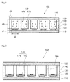
- FIGs. 1 and 2 illustrate cross-sectional views of a transmittance variable film 100 and 200 in accordance with one embodiment of the present disclosure, respectively, which includes a transparent substrate 110, a wire electrode 120, an insulating layer 130, plurality of partition walls 140, a transparent electrode 150, a cell 160, and a charged particle fluid 170.
- Fig. 1 shows a transmittance variable film prior to applying a voltage (OFF mode)
- Fig. 2 shows a transmittance variable film after applying a voltage (ON mode).
- the transparent substrate 110 is configured to secure transparency of the transmittance variable film and impart durability as a support.
- the transparent substrate 110 may be a transparent resin, and include at least one selected from the group consisting of polyethylene terephthalate (PET), polyvinyl chloride (PVC), thermoplastic polyurethane (TPU), and combinations thereof.
- the transparent substrate 110 may be a polyethylene terephthalate (PET), whereby a transmittance variable film 200 having excellent transparency and durability can be achieved.
- the thickness d1 of the transparent substrate 110 may be about 50 ⁇ m to about 200 ⁇ m, and particularly about 120 ⁇ m to about 150 ⁇ m.
- the transparent substrate 110 may provide an excellent durability as a support for the transmittance variable film, and also provide an advantageous effect on the visibility since it prevents unevenness caused by at least in part a warpage of the film.
- the transmittance variable film may include a wire electrode 120 formed on the transparent substrate 110.
- the wire electrode 120 may act as a positive electrode (cathode).
- the wire electrode 120 interacts with charged particles 171 to serve to change transmittance.
- the transmittance variable film 100 when a voltage is applied to the transmittance variable film 100, the charged particles 171 that have been dispersed in the charged particle fluid 170 are assembled on top of the wire electrode 120 by an electrical power, with the transmittance being increased.
- the wire electrode 120 may be formed of a metal-mesh including silver, copper or aluminum.
- the wire electrode 120 may be formed of a metal-mesh including silver, so that it is possible to provide a beneficial effect in terms of the electrical conductivity and the corrosion resistance.
- the wire electrode 120 may be formed through laminating the metal-mesh on the transparent substrate 110 via printing or etching process. As a result, the etching process which results in a severe environmental pollution and the deposition process which consumes lots of energy can be simplified to thereby make the processes environmentally friendly.
- the metal-mesh may have a line width of about 2 ⁇ m to about 20 ⁇ m and a line interval of about 40 ⁇ m to about 300 ⁇ m. Specifically, the metal-mesh may have a line width of about 5 ⁇ m to about 10 ⁇ m and a line interval of about 50 ⁇ m to about 150 ⁇ m.
- the metal-mesh When the metal-mesh satisfies the requirements on the line width and the line interval within the above described ranges, it may be laminated together with the transparent substrate 110, so that a light transmittance of at least about 90% can be secured. Thus, the production cost and production time for the transmittance variable film can be saved, but also sufficient transparency functionally required therefor can be obtained.
- the transmittance variable film 100 and 200 may include an insulating layer 130 formed respectively on the wire electrode 120, as shown in Figs. 1 and 2 .
- an insulating layer 130 formed respectively on the wire electrode 120, as shown in Figs. 1 and 2 .
- the transmittance variable film 100 and 200 may include a plurality of partition walls 140 positioned on both sides of the wire electrode 120.
- the plurality of the partition walls 140 are transparent and serve as a support for the whole structure of the transmittance variable film, and particularly serve to support the transparent electrode 150 formed thereon.
- the plurality of the partition walls may be configured to be a part of a cell 160, which serves as a container having the charged particle fluid therein, whereby a deflection of the charged particles can be prevented.
- Each of the plurality of the partition walls 140 may have a width d2 of about 5 ⁇ m to about 30 ⁇ m, such as about 10 ⁇ m to about 15 ⁇ m.
- the transparent electrode 150 may be rigidly supported, and the deflection of the charged particle fluid can be prevented.
- the plurality of the partition walls 140 may be arranged such that the distance d3 between the adjacent partition walls is about 1000 to about 2000 ⁇ m. This indicates a width of the cell 160.
- the volume of the cell 160 holding sufficient charged particle fluid can be obtained by arranging the plurality of the partition walls 140 at an interval within the above range, which can therefore rigidly support the transparent electrode 150, and at the same time provide excellent variation in transmittance effects.
- the plurality of the partition walls may have a height of about 10 ⁇ m to about 30 ⁇ m, such as about 20 ⁇ m to about 25 ⁇ m.
- Such height d4 of the partition walls means the height of the cell.
- the transmittance variable film can easily be operated at a low voltage (e.g., about 10 V to about 20 V). Further, an initial transmittance can be adjusted by controlling the height, and thereby controlling the amount of the charged particle fluid 170.
- the insulating layer 130 and the plurality of the partition walls 140 may be integrally formed of a same material. As such, the insulating layer 130 and the plurality of the partition walls 140 may be integrally formed of a same material, such that the production cost and the production time can be saved.
- the insulating layer 130 and the partition walls 140 may be a transparent resin, and include at least one selected from the group consisting of urethane acrylate, epoxy acrylate, polyester acrylate, polyether, and combinations thereof, and particularly include at least one of urethane acrylate and epoxy acrylate.
- the insulating layer 130 and the partition walls 140 may include a urethane acrylate resin, so that a transmittance variable film which is strong against an external impact and has excellent durability due to a high elasticity of the urethane acrylate resin can be obtained.
- a transparent electrode 150 may be formed on upper portion of the plurality of the partition walls 140.
- the transparent electrode 150 may act as a negative electrode (anode), and include an indium-tin oxide (ITO), a fluorine-tin oxide (FTO), an aluminum-zinc oxide (AZO), or a gallium-zinc oxide (GZO).
- the transparent electrode 150 may be a front electrode including indium-tin oxide, thereby implementing a higher electrical conductivity.
- the transparent electrode 150 may be formed by coating the oxide on top of the transparent film, and, in particular, prepared by coating an indium-tin oxide (ITO) on upper portion of the transparent film having polyethylene terephthalate (PET) material by means of sputtering deposition.
- ITO indium-tin oxide
- PET polyethylene terephthalate
- the thickness of the transparent electrode 150 may be about 50 to about 200 ⁇ m, and particularly about 120 to about 150 ⁇ m. When the transparent electrode 150 has a thickness within the above described range, the film having an excellent durability and flexibility as well can be achieved.
- the transmittance variable film 100 and 200 may be configured such that the transparent electrode 150 is formed as ITO front electrode and the wire electrode 120 is formed as the metal-mesh, thereby resolving resource depletion and environmental problems and at the same time obtaining an excellent efficiency in the variation in transmittance.
- the transmittance variable film 100 and 200 may include a cell 160 configured to be surrounded by the plurality of the partition walls 140, the insulating layer 130, and the transparent electrode 150, wherein the cell 160 may serve as a container holding the charged particle fluid 170 therein.
- the charged particle fluid 170 refers to a fluid in which a plurality of charged particles 172 is dispersed in a hydrocarbon-based medium 171.
- the plurality of the charged particles 172 may be charged and colored particles.
- Fig. 1 before a voltage is applied to the transmittance variable film 100, the plurality of the charged particles 172 is freely dispersed in the hydrocarbon-based medium 171 to represent a non-transparent property.
- Fig. 2 After a voltage is applied thereto, as shown in Fig. 2 , the plurality of the charged particles 172 is gathered on top of the wire electrode 120, whereby the transmittance of the film is increased.
- the hydrocarbon-based medium 171 is a transparent liquid, which has low volatility, high flash point and non-polar characteristics.
- This hydrocarbon-based medium may include at least one selected from the group consisting of n-dodecane, methyl methacrylate (MMA), undecane, and combinations thereof.
- the hydrocarbon-based medium 171 may include n-dodecane, and thus it is advantageous in that it is not easily evaporated, but helps a smooth dispersion of the charged particles.
- the plurality of the charged particles 172 may have a same charge one another. Specifically, in one embodiment, all of the plurality of the charged particles 172 may have a negative (-) charging property, and the wire electrode 120 may act as a positive electrode (cathode), whereby the plurality of the charged particles 172 may be integrally assembled on the wire electrode 120, whereby excellent variation in transmittance can be accomplished.
- the transmittance variable film may have a variation in transmittance of about 20% to about 70%, particularly about 40% to about 70%, and more particularly about 50% to about 70%, as calculated by the following formula (1).
- the transmittance variable film includes an insulating layer having a thickness of about 0.4 ⁇ m to about 1 ⁇ m, whereby it can have a variation in transmittance within the above range, and can be used in a variety of fields that require high variation in transmittance properties, such as a variety of display devices.
- Variation in transmittance % final transmittance % ⁇ initial transmittance %
- the final transmittance indicates a transmittance of the transmittance variable film as measured after a driving voltage is applied
- the initial transmittance indicates a transmittance of the transmittance variable film as measured before a driving voltage is applied.
- the driving voltage may be about 10 V to about 40 V, such as about 40 V.
- the transmittance variable film includes a wire electrode and an insulating layer having a thickness of about 0.4 ⁇ m to about 1 ⁇ m formed on the wire electrode, whereby the reaction time for the variation in transmittance can be decreased, and excellent variation in transmittance can be achieved even at a low driving voltage.
- a method for producing a transmittance variable film comprising: preparing a transparent substrate; forming a wire electrode on the transparent substrate via printing or etching process; forming an insulating layer and a plurality of partition walls integrally on the transparent substrate and the wire electrode via roll-to-roll process; curing the insulating layer and the plurality of the partition walls; forming a transparent electrode on the plurality of the partition walls; and injecting a charged particle fluid into a cell configured to be surrounded by the plurality of the partition walls, the insulating layer and the transparent electrode, wherein the insulating layer may be formed with a thickness of 0.4 ⁇ m to 1 ⁇ m.
- the wire electrode may be formed by laminating a metal-mesh on the transparent substrate through printing or etching process. The details made on the metal-mesh are as described above.
- the wire electrode may be formed through a printing process, particularly by jetting an ink solution containing a metal powder to form the wire electrode in a form of a metal-mesh.
- finer patterns may be formed, such that the production process may be simplified to reduce the production cost and time.
- the insulating layer and the plurality of the partition walls may be formed by a roll-to-roll process.
- the step of forming the insulating layer and the plurality of the partition walls integrally may include providing a roll around which a mold having a structure of the plurality of the partition walls imprinted therein is wound; applying a resin composition to the roll; and rolling the roll over the transparent substrate.
- the resin composition may include at least one selected from the group consisting of urethane acrylate, epoxy acrylate, polyester acrylate, polyether, and combination thereof. In one embodiment, the resin composition may include at least one of urethane acrylate and epoxy acrylate.
- the insulating layer and the plurality of the partition walls are integrally formed through roll-to-roll process, whereby the production cost and production time can be reduced. Further, the insulating layer may be easily formed with a thickness of 0.4 ⁇ m to 1 ⁇ m, whereby excellent variation in transmittance can also be implemented.
- the transmittance variable film may have 0.4 ⁇ m to 1 ⁇ m thick insulating layer, such that a rapid variation in transmittance can be accomplished even at a low voltage, and the charged particles can be prevented from passing through the electrodes, as well as a short circuit between the anode and the cathode can be avoided.
- the insulating layer and the plurality of the partition walls are integrally formed by the method for producing a transmittance variable film, whereby the production cost and production time can be reduced and also the insulating layer having a thickness of 0.4 ⁇ m to 1 ⁇ m can easily be prepared.
- PET film having a thickness of 120 ⁇ m was provided as a transparent substrate.
- an ink solution containing a silver powder was jetted over the transparent substrate by way of printing in a metal-mesh pattern to thereby form a wire electrode.
- a roll around which a mold having a plurality of partition walls imprinted therein was wound was applied by a resin containing a non-solvent type of urethane acrylate, and subsequently rolled over the transparent substrate and the wire electrode to integrally form the insulating layer of 0.4 ⁇ m thick and the plurality of the partition walls.
- the insulating layer and the partition walls were photo-cured with energy of about 350 mJ/cm 2 .
- a transparent electrode having an indium-tin oxide (ITO) was laminated on the plurality of the partition walls.
- a charged particle fluid into which a plurality of charged particles having a negative (-) charge in a hydrocarbon-based medium was dispersed was injected into a cell configured to be surrounded by the plurality of the partition walls, the insulating layer and the transparent electrode to thereby prepare a transmittance variable film.
- the transmittance variable film was prepared in a similar manner as in Example 1, except that the insulating layer was provided with a thickness of 0.8 ⁇ m.
- the transmittance variable film was prepared in a similar manner as in Example 1, except that the insulating layer was provided with a thickness of 1 ⁇ m.
- the transmittance variable film was prepared in a similar manner as in Example 1, except that the insulating layer was provided with a thickness of 2 ⁇ m.
- the transmittance variable film was prepared in a similar manner as in Example 1, except that the insulating layer was provided with a thickness of 3 ⁇ m.
- the transmittance variable films having an insulating layer of 0.4 ⁇ m to 1 ⁇ m thickness according to Examples 1 to 3 show a higher variation in transmittance compared to the transmittance variable films according to Comparative Examples 1 and 2.
- the transmittance variable films of Examples 1 to 3 can have faster variation in transmittance rates than the transmittance variable films of Comparative Examples 1 and 2, and thereby can show a superior optical function.
Landscapes
- Physics & Mathematics (AREA)
- Nonlinear Science (AREA)
- General Physics & Mathematics (AREA)
- Optics & Photonics (AREA)
- Chemical & Material Sciences (AREA)
- Crystallography & Structural Chemistry (AREA)
- Mathematical Physics (AREA)
- Health & Medical Sciences (AREA)
- Life Sciences & Earth Sciences (AREA)
- Chemical Kinetics & Catalysis (AREA)
- Electrochemistry (AREA)
- Molecular Biology (AREA)
- Electrochromic Elements, Electrophoresis, Or Variable Reflection Or Absorption Elements (AREA)
- Laminated Bodies (AREA)
Abstract
Description
- The present disclosure relates to a transmittance variable film using a voltage and a method for producing the same.
- Conventional transmittance variable film is activated by a polymer dispersed liquid crystal (PDLC) or an electrochromism (EC). In PDLC film, an encapsulated liquid crystal is present in a polymer and the reflectance and transmittance is adjusted by controlling the orientation of the crystal by an electric field. In EC film, the transmittance is adjusted using a material whose color is changed by an electric field. With recent increase of interests in a variety of display devices and functional glasses, there is an increasing trend in interests for a transmittance variable film with a high performance and high energy efficiency.
- One aspect of the present disclosure is to provide a transmittance variable film with excellent variation in transmittance and durability, while it can be driven at a low voltage.
- Another aspect of the present disclosure is to provide a method for producing the transmittance variable film.
- In one embodiment of the present disclosure, there is provided a transmittance variable film, the film comprising: a transparent substrate; a wire electrode formed on the transparent substrate; an insulating layer formed on the wire electrode; a plurality of partition walls positioned on both sides of the wire electrode; a transparent electrode formed on the plurality of the partition walls; a cell configured to be surrounded by the plurality of the partition walls, the insulating layer and the transparent electrode; and a charged particle fluid contained inside the cell, wherein the insulating layer may be formed with a thickness of 0.4 µm to 1 µm.
- In the transmittance variable film, the insulating layer and the partition walls may be integrally formed of a same material.
- The insulating layer and the partition walls may include at least one selected from the group consisting of urethane acrylate, epoxy acrylate, polyester acrylate, polyether, and combinations thereof.
- The wire electrode may be formed of a metal-mesh including silver, copper or aluminum.
- The metal-mesh may have a line width of 2 µm to 20 µm, and a line interval of 40 µm to 300 µm.
- The transparent substrate may include at least one selected from the group consisting of polyethylene terephthalate (PET), polyvinyl chloride (PVC), thermoplastic polyurethane (TPU), and combinations thereof.
- The charged particle fluid may include a plurality of charged particles dispersed in a hydrocarbon-based medium.
- The hydrocarbon-based medium may include at least one selected from the group consisting of n-dodecane, methyl methacrylate (MMA), undecane, and combinations thereof.
- The plurality of the charged particles may have a same charge one another.
- The transparent electrode may include an indium-tin oxide (ITO), a fluorine-tin oxide (FTO), an aluminum-zinc oxide (AZO), or a gallium-zinc oxide (GZO).
- The transmittance variable film may have a variation in transmittance of 20% to 70%, as calculated by the following formula (1):

- In another embodiment of the present disclosure, there is provided a method for producing a transmittance variable film, the method comprising: preparing a transparent substrate; forming a wire electrode on the transparent substrate via printing or etching process; forming an insulating layer and a plurality of partition walls integrally on the transparent substrate and the wire electrode via roll-to-roll process; curing the insulating layer and the plurality of the partition walls; forming a transparent electrode on the plurality of the partition walls; and injecting a charged particle fluid into a cell configured to be surrounded by the plurality of the partition walls, the insulating layer and the transparent electrode, wherein the insulating layer may be formed with a thickness of 0.4 µm to 1 µm.
- The step of forming an insulating layer and a plurality of partition walls integrally may include providing a roll around which a mold with a structure of the plurality of the partition walls imprinted therein is wound; applying a resin composition to the roll; and rolling the roll over the transparent substrate and the wire electrode.
- The resin composition may include at least one selected from the group consisting of urethane acrylate, epoxy acrylate, polyester acrylate, polyether, and combinations thereof.
- The transmittance variable film may implement a fast variation in transmittance even at a low voltage, and is applicable to a glass for a variety of display devices and windows.
- The method for producing a transmittance variable film may provide advantages of saving the production cost and reducing the production time, while at the same time providing a transmittance variable film with a rapid variation rate in the transmittance and high energy efficiency.
- The above and other objects and features of the present disclosure will become apparent from the following description of the disclosure, when taken in conjunction with the accompanying drawings, in which:
-
Fig. 1 shows a transmittance variable film in accordance with one embodiment of the present disclosure, prior to applying a voltage. -
Fig. 2 shows a transmittance variable film after applying a voltage. -
- 100, 200: transmittance variable film
- 110: transparent substrate
- 120: wire electrode
- 130: insulating layer
- 140: partition walls
- 150: transparent electrode
- 160: cell
- 170: charged particle fluid
- 171: hydrocarbon-based medium
- d1: thickness of transparent substrate
- d2: width of partition wall
- d3: interval of partition wall
- d4: height of partition wall
- Hereinafter, exemplary embodiments will be described in detail with reference to the accompanying drawings so as to be easily practiced by a person of ordinary skill in the art. However, It should be understood that the present disclosure is not to be construed as limited to the exemplary embodiments set forth herein and may be embodied in many different forms. Like reference numerals refer to like elements throughout the specification. In the drawings, lengths or thicknesses are enlarged for clarity of various layers and regions. In addition, lengths or thicknesses of some layers and regions are exaggerated for convenience of description.
- Further, it will be understood that when an element such as a layer, region or substrate is referred to as being "on" or extending "onto" another element, it can be directly on or extend directly onto the other element or intervening elements may also be present.
- In one embodiment of the present disclosure, there is provided a transmittance variable film, the film comprising: a transparent substrate; a wire electrode formed on the transparent substrate; an insulating layer formed on the wire electrode; a plurality of partition walls positioned on both sides of the wire electrode; a transparent electrode formed on the plurality of the partition walls; a cell configured to be surrounded by the plurality of the partition walls, the insulating layer and the transparent electrode; and a charged particle fluid contained inside the cell, wherein the insulating layer may be formed with a thickness of 0.4 µm to 1 µm
- In general, when the insulating layer is formed on an electrode with a predetermined thickness to prevent electrons from leaking to the electrode, damages to an electric field generated due to the insulating layer increases a driving voltage for operating an element. Particularly in the case where the element is a transmittance variable film, it leads to a less variation in transmittance, therefore narrowing the application field of the element.
- In order to solve the above mentioned problem, the transmittance variable film may have a wire electrode and an insulating layer formed on the wire electrode, wherein the thickness of the insulating layer may be about 0.4 µm to about 1 µm, whereby rapid variation in the transmittance is possible even at a low driving voltage.
- Particularly, the thickness of the insulating layer may be from about 0.4 µm to about 1 µm, and more particularly about 1 µm. When the thickness of the insulating layer is less than about 0.4 µm, it is difficult to form the insulating layer on the wire electrode, due to which the production process becomes complicated, and further it is difficult to achieve an effect of preventing a charge transfer phenomena. In addition, when the thickness of the insulating layer exceeds about 1 µm, the insulating layer interrupts the flow of an electric field, due to which the driving voltage may be increased to ensure a rapid variation in the transmittance.
- Referring now to
Figs. 1 and 2 , the transmittance variable film will be described in detail.Figs. 1 and 2 illustrate cross-sectional views of atransmittance variable film transparent substrate 110, awire electrode 120, aninsulating layer 130, plurality ofpartition walls 140, atransparent electrode 150, acell 160, and acharged particle fluid 170. Particularly,Fig. 1 shows a transmittance variable film prior to applying a voltage (OFF mode), andFig. 2 shows a transmittance variable film after applying a voltage (ON mode). - The
transparent substrate 110 is configured to secure transparency of the transmittance variable film and impart durability as a support. Thetransparent substrate 110 may be a transparent resin, and include at least one selected from the group consisting of polyethylene terephthalate (PET), polyvinyl chloride (PVC), thermoplastic polyurethane (TPU), and combinations thereof. In one embodiment, thetransparent substrate 110 may be a polyethylene terephthalate (PET), whereby atransmittance variable film 200 having excellent transparency and durability can be achieved. - The thickness d1 of the
transparent substrate 110 may be about 50 µm to about 200 µm, and particularly about 120 µm to about 150 µm. When thetransparent substrate 110 is formed with a thickness within the above range, it may provide an excellent durability as a support for the transmittance variable film, and also provide an advantageous effect on the visibility since it prevents unevenness caused by at least in part a warpage of the film. - The transmittance variable film may include a
wire electrode 120 formed on thetransparent substrate 110. Thewire electrode 120 may act as a positive electrode (cathode). As a voltage is applied, thewire electrode 120 interacts with chargedparticles 171 to serve to change transmittance. Specifically, when a voltage is applied to thetransmittance variable film 100, the chargedparticles 171 that have been dispersed in the chargedparticle fluid 170 are assembled on top of thewire electrode 120 by an electrical power, with the transmittance being increased. - The
wire electrode 120 may be formed of a metal-mesh including silver, copper or aluminum. In one embodiment, thewire electrode 120 may be formed of a metal-mesh including silver, so that it is possible to provide a beneficial effect in terms of the electrical conductivity and the corrosion resistance. In particular, thewire electrode 120 may be formed through laminating the metal-mesh on thetransparent substrate 110 via printing or etching process. As a result, the etching process which results in a severe environmental pollution and the deposition process which consumes lots of energy can be simplified to thereby make the processes environmentally friendly. - The metal-mesh may have a line width of about 2 µm to about 20 µm and a line interval of about 40 µm to about 300 µm. Specifically, the metal-mesh may have a line width of about 5 µm to about 10 µm and a line interval of about 50 µm to about 150 µm. When the metal-mesh satisfies the requirements on the line width and the line interval within the above described ranges, it may be laminated together with the
transparent substrate 110, so that a light transmittance of at least about 90% can be secured. Thus, the production cost and production time for the transmittance variable film can be saved, but also sufficient transparency functionally required therefor can be obtained. - The
transmittance variable film layer 130 formed respectively on thewire electrode 120, as shown inFigs. 1 and 2 . By forming the insulatinglayer 130 on thewire electrode 120, it is possible to prevent a short circuit with thetransparent electrode 150, and also ensure a stable operability and durability since it prevents a direct contact between the wire electrode and the chargedparticles 172 contained in the chargedparticle fluid 170 and avoid the chargedparticles 172 from escaping therethrough. - The
transmittance variable film partition walls 140 positioned on both sides of thewire electrode 120. The plurality of thepartition walls 140 are transparent and serve as a support for the whole structure of the transmittance variable film, and particularly serve to support thetransparent electrode 150 formed thereon. In addition, the plurality of the partition walls may be configured to be a part of acell 160, which serves as a container having the charged particle fluid therein, whereby a deflection of the charged particles can be prevented. - Each of the plurality of the
partition walls 140 may have a width d2 of about 5 µm to about 30 µm, such as about 10 µm to about 15 µm. When each of the plurality of thepartition walls 140 has a thickness within the above range, thetransparent electrode 150 may be rigidly supported, and the deflection of the charged particle fluid can be prevented. - In addition, the plurality of the
partition walls 140 may be arranged such that the distance d3 between the adjacent partition walls is about 1000 to about 2000 µm. This indicates a width of thecell 160. The volume of thecell 160 holding sufficient charged particle fluid can be obtained by arranging the plurality of thepartition walls 140 at an interval within the above range, which can therefore rigidly support thetransparent electrode 150, and at the same time provide excellent variation in transmittance effects. - The plurality of the partition walls may have a height of about 10 µm to about 30 µm, such as about 20 µm to about 25 µm. Such height d4 of the partition walls means the height of the cell. When the plurality of the partition walls have a height within the above range, the transmittance variable film can easily be operated at a low voltage (e.g., about 10 V to about 20 V). Further, an initial transmittance can be adjusted by controlling the height, and thereby controlling the amount of the charged
particle fluid 170. - The insulating
layer 130 and the plurality of thepartition walls 140 may be integrally formed of a same material. As such, the insulatinglayer 130 and the plurality of thepartition walls 140 may be integrally formed of a same material, such that the production cost and the production time can be saved. - The insulating
layer 130 and thepartition walls 140 may be a transparent resin, and include at least one selected from the group consisting of urethane acrylate, epoxy acrylate, polyester acrylate, polyether, and combinations thereof, and particularly include at least one of urethane acrylate and epoxy acrylate. In one embodiment, the insulatinglayer 130 and thepartition walls 140 may include a urethane acrylate resin, so that a transmittance variable film which is strong against an external impact and has excellent durability due to a high elasticity of the urethane acrylate resin can be obtained. - A
transparent electrode 150 may be formed on upper portion of the plurality of thepartition walls 140. Thetransparent electrode 150 may act as a negative electrode (anode), and include an indium-tin oxide (ITO), a fluorine-tin oxide (FTO), an aluminum-zinc oxide (AZO), or a gallium-zinc oxide (GZO). In one embodiment, thetransparent electrode 150 may be a front electrode including indium-tin oxide, thereby implementing a higher electrical conductivity. - The
transparent electrode 150 may be formed by coating the oxide on top of the transparent film, and, in particular, prepared by coating an indium-tin oxide (ITO) on upper portion of the transparent film having polyethylene terephthalate (PET) material by means of sputtering deposition. - The thickness of the
transparent electrode 150 may be about 50 to about 200 µm, and particularly about 120 to about 150 µm. When thetransparent electrode 150 has a thickness within the above described range, the film having an excellent durability and flexibility as well can be achieved. - The
transmittance variable film transparent electrode 150 is formed as ITO front electrode and thewire electrode 120 is formed as the metal-mesh, thereby resolving resource depletion and environmental problems and at the same time obtaining an excellent efficiency in the variation in transmittance. - The
transmittance variable film cell 160 configured to be surrounded by the plurality of thepartition walls 140, the insulatinglayer 130, and thetransparent electrode 150, wherein thecell 160 may serve as a container holding the chargedparticle fluid 170 therein. - The charged
particle fluid 170 refers to a fluid in which a plurality of chargedparticles 172 is dispersed in a hydrocarbon-basedmedium 171. The plurality of the chargedparticles 172 may be charged and colored particles. As shown inFig. 1 , before a voltage is applied to thetransmittance variable film 100, the plurality of the chargedparticles 172 is freely dispersed in the hydrocarbon-basedmedium 171 to represent a non-transparent property. After a voltage is applied thereto, as shown inFig. 2 , the plurality of the chargedparticles 172 is gathered on top of thewire electrode 120, whereby the transmittance of the film is increased. - The hydrocarbon-based
medium 171 is a transparent liquid, which has low volatility, high flash point and non-polar characteristics. This hydrocarbon-based medium may include at least one selected from the group consisting of n-dodecane, methyl methacrylate (MMA), undecane, and combinations thereof. In one embodiment, the hydrocarbon-basedmedium 171 may include n-dodecane, and thus it is advantageous in that it is not easily evaporated, but helps a smooth dispersion of the charged particles. - The plurality of the charged
particles 172 may have a same charge one another. Specifically, in one embodiment, all of the plurality of the chargedparticles 172 may have a negative (-) charging property, and thewire electrode 120 may act as a positive electrode (cathode), whereby the plurality of the chargedparticles 172 may be integrally assembled on thewire electrode 120, whereby excellent variation in transmittance can be accomplished. - The transmittance variable film may have a variation in transmittance of about 20% to about 70%, particularly about 40% to about 70%, and more particularly about 50% to about 70%, as calculated by the following formula (1). The transmittance variable film includes an insulating layer having a thickness of about 0.4 µm to about 1 µm, whereby it can have a variation in transmittance within the above range, and can be used in a variety of fields that require high variation in transmittance properties, such as a variety of display devices.

- In the general formula (1), the final transmittance indicates a transmittance of the transmittance variable film as measured after a driving voltage is applied, and the initial transmittance indicates a transmittance of the transmittance variable film as measured before a driving voltage is applied.
- The driving voltage may be about 10 V to about 40 V, such as about 40 V. The transmittance variable film includes a wire electrode and an insulating layer having a thickness of about 0.4 µm to about 1 µm formed on the wire electrode, whereby the reaction time for the variation in transmittance can be decreased, and excellent variation in transmittance can be achieved even at a low driving voltage.
- In another embodiment of the present disclosure, there is provided a method for producing a transmittance variable film, the method comprising: preparing a transparent substrate; forming a wire electrode on the transparent substrate via printing or etching process; forming an insulating layer and a plurality of partition walls integrally on the transparent substrate and the wire electrode via roll-to-roll process; curing the insulating layer and the plurality of the partition walls; forming a transparent electrode on the plurality of the partition walls; and injecting a charged particle fluid into a cell configured to be surrounded by the plurality of the partition walls, the insulating layer and the transparent electrode, wherein the insulating layer may be formed with a thickness of 0.4 µm to 1 µm.
- The details on the transparent substrate are as previously described.
- In the step of forming the wire electrode, the wire electrode may be formed by laminating a metal-mesh on the transparent substrate through printing or etching process. The details made on the metal-mesh are as described above. In one embodiment, the wire electrode may be formed through a printing process, particularly by jetting an ink solution containing a metal powder to form the wire electrode in a form of a metal-mesh. In forming the wire electrode, by way of a printing process, finer patterns may be formed, such that the production process may be simplified to reduce the production cost and time.
- In the step of forming the insulating layer and the plurality of the partition walls integrally, the insulating layer and the plurality of the partition walls may be formed by a roll-to-roll process. Specifically, the step of forming the insulating layer and the plurality of the partition walls integrally may include providing a roll around which a mold having a structure of the plurality of the partition walls imprinted therein is wound; applying a resin composition to the roll; and rolling the roll over the transparent substrate.
- The resin composition may include at least one selected from the group consisting of urethane acrylate, epoxy acrylate, polyester acrylate, polyether, and combination thereof. In one embodiment, the resin composition may include at least one of urethane acrylate and epoxy acrylate.
- The insulating layer and the plurality of the partition walls are integrally formed through roll-to-roll process, whereby the production cost and production time can be reduced. Further, the insulating layer may be easily formed with a thickness of 0.4 µm to 1 µm, whereby excellent variation in transmittance can also be implemented.
- The transmittance variable film may have 0.4 µm to 1 µm thick insulating layer, such that a rapid variation in transmittance can be accomplished even at a low voltage, and the charged particles can be prevented from passing through the electrodes, as well as a short circuit between the anode and the cathode can be avoided.
- In addition, the insulating layer and the plurality of the partition walls are integrally formed by the method for producing a transmittance variable film, whereby the production cost and production time can be reduced and also the insulating layer having a thickness of 0.4 µm to 1 µm can easily be prepared.
- Hereinafter, exemplary Examples of the present disclosure will now be described. However, it should be noted that while the exemplary examples are listed for explaining the present disclosure, the present disclosure is not limited to these exemplary examples.
- Polyethylene terephthalate (PET) film having a thickness of 120 µm was provided as a transparent substrate. T hen, an ink solution containing a silver powder was jetted over the transparent substrate by way of printing in a metal-mesh pattern to thereby form a wire electrode. Then, a roll around which a mold having a plurality of partition walls imprinted therein was wound was applied by a resin containing a non-solvent type of urethane acrylate, and subsequently rolled over the transparent substrate and the wire electrode to integrally form the insulating layer of 0.4 µm thick and the plurality of the partition walls. Then, the insulating layer and the partition walls were photo-cured with energy of about 350 mJ/cm2. Then, a transparent electrode having an indium-tin oxide (ITO) was laminated on the plurality of the partition walls. Then, a charged particle fluid into which a plurality of charged particles having a negative (-) charge in a hydrocarbon-based medium was dispersed was injected into a cell configured to be surrounded by the plurality of the partition walls, the insulating layer and the transparent electrode to thereby prepare a transmittance variable film.
- The transmittance variable film was prepared in a similar manner as in Example 1, except that the insulating layer was provided with a thickness of 0.8 µm.
- The transmittance variable film was prepared in a similar manner as in Example 1, except that the insulating layer was provided with a thickness of 1 µm.
- The transmittance variable film was prepared in a similar manner as in Example 1, except that the insulating layer was provided with a thickness of 2 µm.
- The transmittance variable film was prepared in a similar manner as in Example 1, except that the insulating layer was provided with a thickness of 3 µm.
- For the transmittance variable films prepared in Examples 1 to 3 and Comparative Examples 1 and 2, initial transmittance and final transmittance were measured at the wavelength of 500 nm using a transmittance measurement apparatus ("haze-gard plus," BYK-Gardner GmbH), and variation in transmittance were calculated by the general formula (1). The results were reported in Table 1 below. The initial transmittance indicates a transmittance of the transmittance variable film prior to applying a voltage to the film, and the final transmittance indicates a transmittance of the transmittance variable film after applying a voltage of about 40 V to the film.

Table 1 Thickness of insulating layer [µm] Variation in transmittance (%) Ex. 1 0.4 50.2 Ex. 2 0.8 47.1 Ex. 3 1 45.3 C. Ex. 1 2 16.3 C. Ex. 2 3 7.9 - As shown in Table 2, it can be seen that the transmittance variable films having an insulating layer of 0.4 µm to 1 µm thickness according to Examples 1 to 3 show a higher variation in transmittance compared to the transmittance variable films according to Comparative Examples 1 and 2. In other words, the transmittance variable films of Examples 1 to 3 can have faster variation in transmittance rates than the transmittance variable films of Comparative Examples 1 and 2, and thereby can show a superior optical function.
- While the preferred examples of the invention have been shown and described, it should be understood that various substitutions, modifications and variations may be made by those skilled in the art without departing from the spirit or scope of the invention. Accordingly, all such modifications and variations are included in the scope of the invention as defined by the following claims.
Claims (14)
- A transmittance variable film, comprising: a transparent substrate; a wire electrode formed on the transparent substrate; an insulating layer formed on the wire electrode; a plurality of partition walls positioned on both sides of the wire electrode; a transparent electrode formed on the plurality of the partition walls; a cell configured to be surrounded by the plurality of the partition walls, the insulating layer and the transparent electrode; and a charged particle fluid contained inside the cell, wherein the insulating layer is formed with a thickness of 0.4 µm to 1 µm.
- The transmittance variable film of claim 1, wherein the insulating layer and the partition walls are integrally formed of a same material.
- The transmittance variable film of claim 1, wherein the insulating layer and the partition walls comprise at least one selected from the group consisting of urethane acrylate, epoxy acrylate, polyester acrylate, polyether, and combinations thereof.
- The transmittance variable film of claim 1, wherein the wire electrode is formed of a metal-mesh comprising silver, copper or aluminum.
- The transmittance variable film of claim 4, wherein the metal-mesh has a line width of 2 µm to 20 µm, and a line interval of 40 µm to 300 µm.
- The transmittance variable film of claim 1, wherein the transparent substrate comprises at least one selected from the group consisting of polyethylene terephthalate (PET), polyvinyl chloride (PVC), thermoplastic polyurethane (TPU), and combinations thereof.
- The transmittance variable film of claim 1, wherein the charged particle fluid comprises a plurality of charged particles dispersed in a hydrocarbon-based medium.
- The transmittance variable film of claim 7, wherein the hydrocarbon-based medium comprises at least one selected from the group consisting of n-dodecane, methyl methacrylate (MMA), undecane, and combinations thereof.
- The transmittance variable film of claim 7, wherein the plurality of the charged particles have a same charge one another.
- The transmittance variable film of claim 1, wherein the transparent electrode comprises an indium-tin oxide (ITO), a fluorine-tin oxide (FTO), an aluminum-zinc oxide (AZO), or a gallium-zinc oxide (GZO).
- The transmittance variable film of claim 1, wherein the transmittance variable film has a variation in transmittance of 20% to 70%, as calculated by the following formula (1):

- A method for producing a transmittance variable film, comprising: preparing a transparent substrate; forming a wire electrode on the transparent substrate via printing or etching process; forming an insulating layer and a plurality of partition walls integrally on the transparent substrate and the wire electrode via roll-to-roll process; curing the insulating layer and the plurality of the partition walls; forming a transparent electrode on the plurality of the partition walls; and injecting a charged particle fluid into a cell configured to be surrounded by the plurality of the partition walls, the insulating layer and the transparent electrode, wherein the insulating layer is formed with a thickness of 0.4 µm to 1 µm.
- The method for producing a transmittance variable film of claim 12, wherein the step of forming an insulating layer and a plurality of partition walls integrally comprises providing a roll around which a mold having a structure of the plurality of the partition walls imprinted therein is wound; applying a resin composition to the roll; and rolling the roll over the transparent substrate and the wire electrode.
- The method for producing a transmittance variable film of claim 13, wherein the resin composition comprises at least one selected from the group consisting of urethane acrylate, epoxy acrylate, polyester acrylate, polyether, and combinations thereof.
Applications Claiming Priority (2)
| Application Number | Priority Date | Filing Date | Title |
|---|---|---|---|
| KR1020130146486A KR20150062240A (en) | 2013-11-28 | 2013-11-28 | Transmissivity-changeable film and method of manufacturing the same |
| PCT/KR2014/010189 WO2015080385A1 (en) | 2013-11-28 | 2014-10-28 | Transmittance-variable film and method for producing same |
Publications (3)
| Publication Number | Publication Date |
|---|---|
| EP3076227A1 true EP3076227A1 (en) | 2016-10-05 |
| EP3076227A4 EP3076227A4 (en) | 2016-12-07 |
| EP3076227B1 EP3076227B1 (en) | 2018-07-04 |
Family
ID=53199295
Family Applications (1)
| Application Number | Title | Priority Date | Filing Date |
|---|---|---|---|
| EP14865494.0A Not-in-force EP3076227B1 (en) | 2013-11-28 | 2014-10-28 | Transmittance-variable film and method for producing same |
Country Status (7)
| Country | Link |
|---|---|
| US (1) | US10067399B2 (en) |
| EP (1) | EP3076227B1 (en) |
| JP (1) | JP6655535B2 (en) |
| KR (1) | KR20150062240A (en) |
| CN (1) | CN105793768B (en) |
| TW (1) | TWI629538B (en) |
| WO (1) | WO2015080385A1 (en) |
Families Citing this family (10)
| Publication number | Priority date | Publication date | Assignee | Title |
|---|---|---|---|---|
| KR102070571B1 (en) * | 2016-09-09 | 2020-01-29 | 주식회사 엘지화학 | A Device having changeable transparency |
| KR102184385B1 (en) * | 2017-11-03 | 2020-11-30 | 주식회사 엘지화학 | Transmittance controllable device |
| KR102056597B1 (en) * | 2017-11-03 | 2019-12-17 | 주식회사 엘지화학 | Transmittance controllable film |
| KR102184389B1 (en) * | 2017-11-03 | 2020-11-30 | 주식회사 엘지화학 | Transmittance controllable device |
| KR102179729B1 (en) * | 2018-03-27 | 2020-11-17 | 주식회사 엘지화학 | Black partition wall pattern film and method for manufacturing thereof |
| CN108776405B (en) * | 2018-05-30 | 2020-11-24 | 东华大学 | Multi-state smart window, preparation method thereof, and multi-pattern smart window prepared therefrom |
| ES2984320T3 (en) | 2018-06-28 | 2024-10-29 | E Ink Corp | Methods for driving variable transmission electrophoretic media |
| TWI764243B (en) * | 2020-08-20 | 2022-05-11 | 元太科技工業股份有限公司 | Electrophoretic display device |
| CN114077113A (en) * | 2020-08-20 | 2022-02-22 | 元太科技工业股份有限公司 | Electrophoretic display device |
| KR20240068881A (en) * | 2022-11-09 | 2024-05-20 | 삼성디스플레이 주식회사 | Display Apparatus |
Family Cites Families (22)
| Publication number | Priority date | Publication date | Assignee | Title |
|---|---|---|---|---|
| JPH0329834U (en) * | 1989-04-14 | 1991-03-25 | ||
| JP3116844B2 (en) * | 1996-06-21 | 2000-12-11 | 日本電気株式会社 | Color plasma display panel and method of manufacturing the same |
| US5903382A (en) | 1997-12-19 | 1999-05-11 | Rockwell International Corporation | Electrodeposition cell with high light transmission |
| JP3554222B2 (en) * | 1999-05-18 | 2004-08-18 | キヤノン株式会社 | Display device |
| US6672921B1 (en) | 2000-03-03 | 2004-01-06 | Sipix Imaging, Inc. | Manufacturing process for electrophoretic display |
| US6829078B2 (en) | 2000-03-03 | 2004-12-07 | Sipix Imaging Inc. | Electrophoretic display and novel process for its manufacture |
| JP3667242B2 (en) * | 2000-04-13 | 2005-07-06 | キヤノン株式会社 | Electrophoretic display method and electrophoretic display device |
| KR100417258B1 (en) | 2001-06-13 | 2004-02-11 | 주식회사 미라클 | a portable phone keypad and manufacturing method thereof |
| TW539928B (en) * | 2001-08-20 | 2003-07-01 | Sipix Imaging Inc | An improved transflective electrophoretic display |
| JP4024172B2 (en) * | 2003-03-19 | 2007-12-19 | 株式会社日立製作所 | Electrophoretic display device and manufacturing method |
| US7880958B2 (en) * | 2005-09-23 | 2011-02-01 | Sipix Imaging, Inc. | Display cell structure and electrode protecting layer compositions |
| CN101246911B (en) * | 2008-03-10 | 2010-06-09 | 北京航空航天大学 | A metal microgrid transparent electrode and its preparation method |
| JP2011002695A (en) | 2009-06-19 | 2011-01-06 | Konica Minolta Business Technologies Inc | Display particle for image display device, and image display device |
| KR101085570B1 (en) * | 2010-03-15 | 2011-11-25 | 한국생산기술연구원 | Method of manufacturing an electronic paper display device including an insulating layer |
| KR101123952B1 (en) * | 2010-03-15 | 2012-03-23 | 한국생산기술연구원 | Electronic paper display apparatus comprising dielectric layer |
| KR20120121121A (en) | 2011-04-26 | 2012-11-05 | 서울시립대학교 산학협력단 | E-Papar ane method of manufacturing the same |
| KR101241306B1 (en) * | 2010-07-29 | 2013-03-11 | 주식회사 이미지앤머터리얼스 | Window filter sheet and window assembly using the same |
| JP5547015B2 (en) * | 2010-09-28 | 2014-07-09 | 三菱鉛筆株式会社 | White particles for electrophoretic ink and electrophoretic ink using the same |
| JP2012252091A (en) * | 2011-06-01 | 2012-12-20 | Sony Corp | Display apparatus |
| EP2761360A4 (en) | 2011-09-30 | 2015-06-10 | 3M Innovative Properties Co | Electronically switchable privacy film and display device having same |
| JP5991012B2 (en) | 2012-05-08 | 2016-09-14 | セイコーエプソン株式会社 | Display device and manufacturing method of display device |
| CN103278955B (en) * | 2012-12-14 | 2015-11-11 | 上海天马微电子有限公司 | Color film substrate and touch liquid crystal display device |
-
2013
- 2013-11-28 KR KR1020130146486A patent/KR20150062240A/en not_active Ceased
-
2014
- 2014-10-28 JP JP2016534730A patent/JP6655535B2/en not_active Expired - Fee Related
- 2014-10-28 US US15/039,394 patent/US10067399B2/en not_active Expired - Fee Related
- 2014-10-28 CN CN201480065406.6A patent/CN105793768B/en not_active Expired - Fee Related
- 2014-10-28 WO PCT/KR2014/010189 patent/WO2015080385A1/en not_active Ceased
- 2014-10-28 EP EP14865494.0A patent/EP3076227B1/en not_active Not-in-force
- 2014-10-31 TW TW103137812A patent/TWI629538B/en not_active IP Right Cessation
Also Published As
| Publication number | Publication date |
|---|---|
| CN105793768B (en) | 2019-07-09 |
| EP3076227B1 (en) | 2018-07-04 |
| KR20150062240A (en) | 2015-06-08 |
| CN105793768A (en) | 2016-07-20 |
| TW201520640A (en) | 2015-06-01 |
| JP6655535B2 (en) | 2020-02-26 |
| EP3076227A4 (en) | 2016-12-07 |
| TWI629538B (en) | 2018-07-11 |
| WO2015080385A1 (en) | 2015-06-04 |
| JP2016540249A (en) | 2016-12-22 |
| US10067399B2 (en) | 2018-09-04 |
| US20170153525A1 (en) | 2017-06-01 |
Similar Documents
| Publication | Publication Date | Title |
|---|---|---|
| EP3076227B1 (en) | Transmittance-variable film and method for producing same | |
| US9869918B2 (en) | Electrochromic apparatus, electrochromic element, and method of manufacturing electrochromic element | |
| KR101127277B1 (en) | Electrode for electrochromic device and electrochromic device having the same | |
| EP4055442A1 (en) | Three-dimensional, color-changing objects including a light-transmissive substrate and an electrophoretic medium | |
| US20240201555A1 (en) | Method of production of an electro-optic device comprising integrated conductive edge seal | |
| CN114868079B (en) | Electrophoretic display layer with thin film upper electrode | |
| EP3598219B1 (en) | Barrier rib pattern film and manufacturing method therefor | |
| EP3654095A1 (en) | Electrochromic films with edge protection | |
| US9971223B2 (en) | Display substrate, display apparatus having the same, and fabricating method thereof | |
| US8654431B2 (en) | Active matrix electrochromic device and method of manufacturing the same | |
| KR20130056491A (en) | Electrochromism film | |
| CN105807451A (en) | Intelligent light adjusting film based on graphene/organic matter composite transparent conductive film | |
| CN103399443B (en) | Electrochromic display panel and preparation method thereof, display device | |
| US8873130B2 (en) | Electronic paper display device and method of fabricating the same | |
| US20090155544A1 (en) | Web-like electrode material and method for producing same | |
| CN115407575A (en) | Electrochromic device and manufacturing method thereof | |
| JP5316701B2 (en) | Electrochemical display element | |
| KR20230099657A (en) | electrochromic device | |
| CN106292116A (en) | Display floater and manufacture method, display device | |
| KR20030067021A (en) | Passive matrix electorchromic display using electrochromic matrial and manufacturing method thereof | |
| US10042216B2 (en) | Array substrate and manufacturing method thereof, liquid crystal panel and liquid crystal display device | |
| CN103365472A (en) | Polarized light and light filtering module and touch display screen | |
| CN102890381A (en) | Electrochromic device and preparation method thereof | |
| KR20260014673A (en) | Electro-optical device having an electrophoretic medium comprising an organic electroactive compound | |
| KR20220004427A (en) | Electrochromic device comprising inorganic coating layer formed on the electrochromic layer |
Legal Events
| Date | Code | Title | Description |
|---|---|---|---|
| PUAI | Public reference made under article 153(3) epc to a published international application that has entered the european phase |
Free format text: ORIGINAL CODE: 0009012 |
|
| 17P | Request for examination filed |
Effective date: 20160628 |
|
| AK | Designated contracting states |
Kind code of ref document: A1 Designated state(s): AL AT BE BG CH CY CZ DE DK EE ES FI FR GB GR HR HU IE IS IT LI LT LU LV MC MK MT NL NO PL PT RO RS SE SI SK SM TR |
|
| AX | Request for extension of the european patent |
Extension state: BA ME |
|
| REG | Reference to a national code |
Ref country code: DE Ref legal event code: R079 Ref document number: 602014028097 Country of ref document: DE Free format text: PREVIOUS MAIN CLASS: G02F0001010000 Ipc: G02F0001167000 |
|
| A4 | Supplementary search report drawn up and despatched |
Effective date: 20161107 |
|
| RIC1 | Information provided on ipc code assigned before grant |
Ipc: G02F 1/167 20060101AFI20161031BHEP |
|
| DAX | Request for extension of the european patent (deleted) | ||
| GRAP | Despatch of communication of intention to grant a patent |
Free format text: ORIGINAL CODE: EPIDOSNIGR1 |
|
| INTG | Intention to grant announced |
Effective date: 20180130 |
|
| GRAS | Grant fee paid |
Free format text: ORIGINAL CODE: EPIDOSNIGR3 |
|
| GRAA | (expected) grant |
Free format text: ORIGINAL CODE: 0009210 |
|
| AK | Designated contracting states |
Kind code of ref document: B1 Designated state(s): AL AT BE BG CH CY CZ DE DK EE ES FI FR GB GR HR HU IE IS IT LI LT LU LV MC MK MT NL NO PL PT RO RS SE SI SK SM TR |
|
| REG | Reference to a national code |
Ref country code: GB Ref legal event code: FG4D |
|
| REG | Reference to a national code |
Ref country code: CH Ref legal event code: EP |
|
| REG | Reference to a national code |
Ref country code: AT Ref legal event code: REF Ref document number: 1015126 Country of ref document: AT Kind code of ref document: T Effective date: 20180715 |
|
| REG | Reference to a national code |
Ref country code: IE Ref legal event code: FG4D |
|
| REG | Reference to a national code |
Ref country code: DE Ref legal event code: R096 Ref document number: 602014028097 Country of ref document: DE |
|
| REG | Reference to a national code |
Ref country code: NL Ref legal event code: MP Effective date: 20180704 |
|
| REG | Reference to a national code |
Ref country code: LT Ref legal event code: MG4D |
|
| REG | Reference to a national code |
Ref country code: AT Ref legal event code: MK05 Ref document number: 1015126 Country of ref document: AT Kind code of ref document: T Effective date: 20180704 |
|
| PG25 | Lapsed in a contracting state [announced via postgrant information from national office to epo] |
Ref country code: NL Free format text: LAPSE BECAUSE OF FAILURE TO SUBMIT A TRANSLATION OF THE DESCRIPTION OR TO PAY THE FEE WITHIN THE PRESCRIBED TIME-LIMIT Effective date: 20180704 |
|
| PG25 | Lapsed in a contracting state [announced via postgrant information from national office to epo] |
Ref country code: AT Free format text: LAPSE BECAUSE OF FAILURE TO SUBMIT A TRANSLATION OF THE DESCRIPTION OR TO PAY THE FEE WITHIN THE PRESCRIBED TIME-LIMIT Effective date: 20180704 Ref country code: SE Free format text: LAPSE BECAUSE OF FAILURE TO SUBMIT A TRANSLATION OF THE DESCRIPTION OR TO PAY THE FEE WITHIN THE PRESCRIBED TIME-LIMIT Effective date: 20180704 Ref country code: IS Free format text: LAPSE BECAUSE OF FAILURE TO SUBMIT A TRANSLATION OF THE DESCRIPTION OR TO PAY THE FEE WITHIN THE PRESCRIBED TIME-LIMIT Effective date: 20181104 Ref country code: BG Free format text: LAPSE BECAUSE OF FAILURE TO SUBMIT A TRANSLATION OF THE DESCRIPTION OR TO PAY THE FEE WITHIN THE PRESCRIBED TIME-LIMIT Effective date: 20181004 Ref country code: GR Free format text: LAPSE BECAUSE OF FAILURE TO SUBMIT A TRANSLATION OF THE DESCRIPTION OR TO PAY THE FEE WITHIN THE PRESCRIBED TIME-LIMIT Effective date: 20181005 Ref country code: NO Free format text: LAPSE BECAUSE OF FAILURE TO SUBMIT A TRANSLATION OF THE DESCRIPTION OR TO PAY THE FEE WITHIN THE PRESCRIBED TIME-LIMIT Effective date: 20181004 Ref country code: LT Free format text: LAPSE BECAUSE OF FAILURE TO SUBMIT A TRANSLATION OF THE DESCRIPTION OR TO PAY THE FEE WITHIN THE PRESCRIBED TIME-LIMIT Effective date: 20180704 Ref country code: RS Free format text: LAPSE BECAUSE OF FAILURE TO SUBMIT A TRANSLATION OF THE DESCRIPTION OR TO PAY THE FEE WITHIN THE PRESCRIBED TIME-LIMIT Effective date: 20180704 Ref country code: PL Free format text: LAPSE BECAUSE OF FAILURE TO SUBMIT A TRANSLATION OF THE DESCRIPTION OR TO PAY THE FEE WITHIN THE PRESCRIBED TIME-LIMIT Effective date: 20180704 Ref country code: CZ Free format text: LAPSE BECAUSE OF FAILURE TO SUBMIT A TRANSLATION OF THE DESCRIPTION OR TO PAY THE FEE WITHIN THE PRESCRIBED TIME-LIMIT Effective date: 20180704 Ref country code: FI Free format text: LAPSE BECAUSE OF FAILURE TO SUBMIT A TRANSLATION OF THE DESCRIPTION OR TO PAY THE FEE WITHIN THE PRESCRIBED TIME-LIMIT Effective date: 20180704 |
|
| PG25 | Lapsed in a contracting state [announced via postgrant information from national office to epo] |
Ref country code: LV Free format text: LAPSE BECAUSE OF FAILURE TO SUBMIT A TRANSLATION OF THE DESCRIPTION OR TO PAY THE FEE WITHIN THE PRESCRIBED TIME-LIMIT Effective date: 20180704 Ref country code: AL Free format text: LAPSE BECAUSE OF FAILURE TO SUBMIT A TRANSLATION OF THE DESCRIPTION OR TO PAY THE FEE WITHIN THE PRESCRIBED TIME-LIMIT Effective date: 20180704 Ref country code: ES Free format text: LAPSE BECAUSE OF FAILURE TO SUBMIT A TRANSLATION OF THE DESCRIPTION OR TO PAY THE FEE WITHIN THE PRESCRIBED TIME-LIMIT Effective date: 20180704 Ref country code: HR Free format text: LAPSE BECAUSE OF FAILURE TO SUBMIT A TRANSLATION OF THE DESCRIPTION OR TO PAY THE FEE WITHIN THE PRESCRIBED TIME-LIMIT Effective date: 20180704 |
|
| REG | Reference to a national code |
Ref country code: DE Ref legal event code: R097 Ref document number: 602014028097 Country of ref document: DE |
|
| PG25 | Lapsed in a contracting state [announced via postgrant information from national office to epo] |
Ref country code: IT Free format text: LAPSE BECAUSE OF FAILURE TO SUBMIT A TRANSLATION OF THE DESCRIPTION OR TO PAY THE FEE WITHIN THE PRESCRIBED TIME-LIMIT Effective date: 20180704 Ref country code: EE Free format text: LAPSE BECAUSE OF FAILURE TO SUBMIT A TRANSLATION OF THE DESCRIPTION OR TO PAY THE FEE WITHIN THE PRESCRIBED TIME-LIMIT Effective date: 20180704 Ref country code: RO Free format text: LAPSE BECAUSE OF FAILURE TO SUBMIT A TRANSLATION OF THE DESCRIPTION OR TO PAY THE FEE WITHIN THE PRESCRIBED TIME-LIMIT Effective date: 20180704 |
|
| PLBE | No opposition filed within time limit |
Free format text: ORIGINAL CODE: 0009261 |
|
| STAA | Information on the status of an ep patent application or granted ep patent |
Free format text: STATUS: NO OPPOSITION FILED WITHIN TIME LIMIT |
|
| PG25 | Lapsed in a contracting state [announced via postgrant information from national office to epo] |
Ref country code: SK Free format text: LAPSE BECAUSE OF FAILURE TO SUBMIT A TRANSLATION OF THE DESCRIPTION OR TO PAY THE FEE WITHIN THE PRESCRIBED TIME-LIMIT Effective date: 20180704 Ref country code: SM Free format text: LAPSE BECAUSE OF FAILURE TO SUBMIT A TRANSLATION OF THE DESCRIPTION OR TO PAY THE FEE WITHIN THE PRESCRIBED TIME-LIMIT Effective date: 20180704 Ref country code: DK Free format text: LAPSE BECAUSE OF FAILURE TO SUBMIT A TRANSLATION OF THE DESCRIPTION OR TO PAY THE FEE WITHIN THE PRESCRIBED TIME-LIMIT Effective date: 20180704 |
|
| REG | Reference to a national code |
Ref country code: CH Ref legal event code: PL |
|
| 26N | No opposition filed |
Effective date: 20190405 |
|
| GBPC | Gb: european patent ceased through non-payment of renewal fee |
Effective date: 20181028 |
|
| REG | Reference to a national code |
Ref country code: BE Ref legal event code: MM Effective date: 20181031 |
|
| PG25 | Lapsed in a contracting state [announced via postgrant information from national office to epo] |
Ref country code: MC Free format text: LAPSE BECAUSE OF FAILURE TO SUBMIT A TRANSLATION OF THE DESCRIPTION OR TO PAY THE FEE WITHIN THE PRESCRIBED TIME-LIMIT Effective date: 20180704 Ref country code: LU Free format text: LAPSE BECAUSE OF NON-PAYMENT OF DUE FEES Effective date: 20181028 |
|
| REG | Reference to a national code |
Ref country code: IE Ref legal event code: MM4A |
|
| PG25 | Lapsed in a contracting state [announced via postgrant information from national office to epo] |
Ref country code: CH Free format text: LAPSE BECAUSE OF NON-PAYMENT OF DUE FEES Effective date: 20181031 Ref country code: LI Free format text: LAPSE BECAUSE OF NON-PAYMENT OF DUE FEES Effective date: 20181031 Ref country code: FR Free format text: LAPSE BECAUSE OF NON-PAYMENT OF DUE FEES Effective date: 20181031 Ref country code: SI Free format text: LAPSE BECAUSE OF FAILURE TO SUBMIT A TRANSLATION OF THE DESCRIPTION OR TO PAY THE FEE WITHIN THE PRESCRIBED TIME-LIMIT Effective date: 20180704 Ref country code: BE Free format text: LAPSE BECAUSE OF NON-PAYMENT OF DUE FEES Effective date: 20181031 |
|
| PG25 | Lapsed in a contracting state [announced via postgrant information from national office to epo] |
Ref country code: GB Free format text: LAPSE BECAUSE OF NON-PAYMENT OF DUE FEES Effective date: 20181028 Ref country code: IE Free format text: LAPSE BECAUSE OF NON-PAYMENT OF DUE FEES Effective date: 20181028 |
|
| PG25 | Lapsed in a contracting state [announced via postgrant information from national office to epo] |
Ref country code: MT Free format text: LAPSE BECAUSE OF NON-PAYMENT OF DUE FEES Effective date: 20181028 |
|
| PGFP | Annual fee paid to national office [announced via postgrant information from national office to epo] |
Ref country code: DE Payment date: 20190905 Year of fee payment: 6 |
|
| PG25 | Lapsed in a contracting state [announced via postgrant information from national office to epo] |
Ref country code: TR Free format text: LAPSE BECAUSE OF FAILURE TO SUBMIT A TRANSLATION OF THE DESCRIPTION OR TO PAY THE FEE WITHIN THE PRESCRIBED TIME-LIMIT Effective date: 20180704 |
|
| PG25 | Lapsed in a contracting state [announced via postgrant information from national office to epo] |
Ref country code: PT Free format text: LAPSE BECAUSE OF FAILURE TO SUBMIT A TRANSLATION OF THE DESCRIPTION OR TO PAY THE FEE WITHIN THE PRESCRIBED TIME-LIMIT Effective date: 20180704 |
|
| PG25 | Lapsed in a contracting state [announced via postgrant information from national office to epo] |
Ref country code: HU Free format text: LAPSE BECAUSE OF FAILURE TO SUBMIT A TRANSLATION OF THE DESCRIPTION OR TO PAY THE FEE WITHIN THE PRESCRIBED TIME-LIMIT; INVALID AB INITIO Effective date: 20141028 Ref country code: MK Free format text: LAPSE BECAUSE OF NON-PAYMENT OF DUE FEES Effective date: 20180704 Ref country code: CY Free format text: LAPSE BECAUSE OF FAILURE TO SUBMIT A TRANSLATION OF THE DESCRIPTION OR TO PAY THE FEE WITHIN THE PRESCRIBED TIME-LIMIT Effective date: 20180704 |
|
| REG | Reference to a national code |
Ref country code: DE Ref legal event code: R119 Ref document number: 602014028097 Country of ref document: DE |
|
| PG25 | Lapsed in a contracting state [announced via postgrant information from national office to epo] |
Ref country code: DE Free format text: LAPSE BECAUSE OF NON-PAYMENT OF DUE FEES Effective date: 20210501 |