EP3073550A1 - Connection structure for electrical storage element group - Google Patents
Connection structure for electrical storage element group Download PDFInfo
- Publication number
- EP3073550A1 EP3073550A1 EP14864034.5A EP14864034A EP3073550A1 EP 3073550 A1 EP3073550 A1 EP 3073550A1 EP 14864034 A EP14864034 A EP 14864034A EP 3073550 A1 EP3073550 A1 EP 3073550A1
- Authority
- EP
- European Patent Office
- Prior art keywords
- electrical storage
- storage element
- connecting member
- element groups
- terminal
- Prior art date
- Legal status (The legal status is an assumption and is not a legal conclusion. Google has not performed a legal analysis and makes no representation as to the accuracy of the status listed.)
- Granted
Links
Images


Classifications
-
- H—ELECTRICITY
- H01—ELECTRIC ELEMENTS
- H01G—CAPACITORS; CAPACITORS, RECTIFIERS, DETECTORS, SWITCHING DEVICES, LIGHT-SENSITIVE OR TEMPERATURE-SENSITIVE DEVICES OF THE ELECTROLYTIC TYPE
- H01G11/00—Hybrid capacitors, i.e. capacitors having different positive and negative electrodes; Electric double-layer [EDL] capacitors; Processes for the manufacture thereof or of parts thereof
- H01G11/10—Multiple hybrid or EDL capacitors, e.g. arrays or modules
-
- H—ELECTRICITY
- H01—ELECTRIC ELEMENTS
- H01G—CAPACITORS; CAPACITORS, RECTIFIERS, DETECTORS, SWITCHING DEVICES, LIGHT-SENSITIVE OR TEMPERATURE-SENSITIVE DEVICES OF THE ELECTROLYTIC TYPE
- H01G11/00—Hybrid capacitors, i.e. capacitors having different positive and negative electrodes; Electric double-layer [EDL] capacitors; Processes for the manufacture thereof or of parts thereof
- H01G11/74—Terminals, e.g. extensions of current collectors
- H01G11/76—Terminals, e.g. extensions of current collectors specially adapted for integration in multiple or stacked hybrid or EDL capacitors
-
- H—ELECTRICITY
- H01—ELECTRIC ELEMENTS
- H01M—PROCESSES OR MEANS, e.g. BATTERIES, FOR THE DIRECT CONVERSION OF CHEMICAL ENERGY INTO ELECTRICAL ENERGY
- H01M50/00—Constructional details or processes of manufacture of the non-active parts of electrochemical cells other than fuel cells, e.g. hybrid cells
- H01M50/20—Mountings; Secondary casings or frames; Racks, modules or packs; Suspension devices; Shock absorbers; Transport or carrying devices; Holders
- H01M50/204—Racks, modules or packs for multiple batteries or multiple cells
- H01M50/207—Racks, modules or packs for multiple batteries or multiple cells characterised by their shape
- H01M50/209—Racks, modules or packs for multiple batteries or multiple cells characterised by their shape adapted for prismatic or rectangular cells
-
- H—ELECTRICITY
- H01—ELECTRIC ELEMENTS
- H01M—PROCESSES OR MEANS, e.g. BATTERIES, FOR THE DIRECT CONVERSION OF CHEMICAL ENERGY INTO ELECTRICAL ENERGY
- H01M50/00—Constructional details or processes of manufacture of the non-active parts of electrochemical cells other than fuel cells, e.g. hybrid cells
- H01M50/50—Current conducting connections for cells or batteries
- H01M50/502—Interconnectors for connecting terminals of adjacent batteries; Interconnectors for connecting cells outside a battery casing
- H01M50/509—Interconnectors for connecting terminals of adjacent batteries; Interconnectors for connecting cells outside a battery casing characterised by the type of connection, e.g. mixed connections
- H01M50/51—Connection only in series
-
- H—ELECTRICITY
- H01—ELECTRIC ELEMENTS
- H01M—PROCESSES OR MEANS, e.g. BATTERIES, FOR THE DIRECT CONVERSION OF CHEMICAL ENERGY INTO ELECTRICAL ENERGY
- H01M50/00—Constructional details or processes of manufacture of the non-active parts of electrochemical cells other than fuel cells, e.g. hybrid cells
- H01M50/50—Current conducting connections for cells or batteries
- H01M50/502—Interconnectors for connecting terminals of adjacent batteries; Interconnectors for connecting cells outside a battery casing
- H01M50/514—Methods for interconnecting adjacent batteries or cells
- H01M50/517—Methods for interconnecting adjacent batteries or cells by fixing means, e.g. screws, rivets or bolts
-
- H—ELECTRICITY
- H01—ELECTRIC ELEMENTS
- H01M—PROCESSES OR MEANS, e.g. BATTERIES, FOR THE DIRECT CONVERSION OF CHEMICAL ENERGY INTO ELECTRICAL ENERGY
- H01M50/00—Constructional details or processes of manufacture of the non-active parts of electrochemical cells other than fuel cells, e.g. hybrid cells
- H01M50/50—Current conducting connections for cells or batteries
- H01M50/502—Interconnectors for connecting terminals of adjacent batteries; Interconnectors for connecting cells outside a battery casing
- H01M50/521—Interconnectors for connecting terminals of adjacent batteries; Interconnectors for connecting cells outside a battery casing characterised by the material
- H01M50/524—Organic material
-
- H—ELECTRICITY
- H01—ELECTRIC ELEMENTS
- H01M—PROCESSES OR MEANS, e.g. BATTERIES, FOR THE DIRECT CONVERSION OF CHEMICAL ENERGY INTO ELECTRICAL ENERGY
- H01M50/00—Constructional details or processes of manufacture of the non-active parts of electrochemical cells other than fuel cells, e.g. hybrid cells
- H01M50/50—Current conducting connections for cells or batteries
- H01M50/572—Means for preventing undesired use or discharge
- H01M50/584—Means for preventing undesired use or discharge for preventing incorrect connections inside or outside the batteries
- H01M50/588—Means for preventing undesired use or discharge for preventing incorrect connections inside or outside the batteries outside the batteries, e.g. incorrect connections of terminals or busbars
-
- H—ELECTRICITY
- H01—ELECTRIC ELEMENTS
- H01G—CAPACITORS; CAPACITORS, RECTIFIERS, DETECTORS, SWITCHING DEVICES, LIGHT-SENSITIVE OR TEMPERATURE-SENSITIVE DEVICES OF THE ELECTROLYTIC TYPE
- H01G2/00—Details of capacitors not covered by a single one of groups H01G4/00-H01G11/00
- H01G2/02—Mountings
- H01G2/04—Mountings specially adapted for mounting on a chassis
-
- H—ELECTRICITY
- H01—ELECTRIC ELEMENTS
- H01M—PROCESSES OR MEANS, e.g. BATTERIES, FOR THE DIRECT CONVERSION OF CHEMICAL ENERGY INTO ELECTRICAL ENERGY
- H01M2220/00—Batteries for particular applications
- H01M2220/20—Batteries in motive systems, e.g. vehicle, ship, plane
-
- H—ELECTRICITY
- H01—ELECTRIC ELEMENTS
- H01M—PROCESSES OR MEANS, e.g. BATTERIES, FOR THE DIRECT CONVERSION OF CHEMICAL ENERGY INTO ELECTRICAL ENERGY
- H01M50/00—Constructional details or processes of manufacture of the non-active parts of electrochemical cells other than fuel cells, e.g. hybrid cells
- H01M50/50—Current conducting connections for cells or batteries
- H01M50/569—Constructional details of current conducting connections for detecting conditions inside cells or batteries, e.g. details of voltage sensing terminals
-
- Y—GENERAL TAGGING OF NEW TECHNOLOGICAL DEVELOPMENTS; GENERAL TAGGING OF CROSS-SECTIONAL TECHNOLOGIES SPANNING OVER SEVERAL SECTIONS OF THE IPC; TECHNICAL SUBJECTS COVERED BY FORMER USPC CROSS-REFERENCE ART COLLECTIONS [XRACs] AND DIGESTS
- Y02—TECHNOLOGIES OR APPLICATIONS FOR MITIGATION OR ADAPTATION AGAINST CLIMATE CHANGE
- Y02E—REDUCTION OF GREENHOUSE GAS [GHG] EMISSIONS, RELATED TO ENERGY GENERATION, TRANSMISSION OR DISTRIBUTION
- Y02E60/00—Enabling technologies; Technologies with a potential or indirect contribution to GHG emissions mitigation
- Y02E60/10—Energy storage using batteries
-
- Y—GENERAL TAGGING OF NEW TECHNOLOGICAL DEVELOPMENTS; GENERAL TAGGING OF CROSS-SECTIONAL TECHNOLOGIES SPANNING OVER SEVERAL SECTIONS OF THE IPC; TECHNICAL SUBJECTS COVERED BY FORMER USPC CROSS-REFERENCE ART COLLECTIONS [XRACs] AND DIGESTS
- Y02—TECHNOLOGIES OR APPLICATIONS FOR MITIGATION OR ADAPTATION AGAINST CLIMATE CHANGE
- Y02E—REDUCTION OF GREENHOUSE GAS [GHG] EMISSIONS, RELATED TO ENERGY GENERATION, TRANSMISSION OR DISTRIBUTION
- Y02E60/00—Enabling technologies; Technologies with a potential or indirect contribution to GHG emissions mitigation
- Y02E60/13—Energy storage using capacitors
Definitions
- the present invention may be configured as follows.
- the linking portion of the connecting member may include a locking portion to be locked to the holding portion of the insulation protector.
- connection structure for electrical storage element groups reduced in cost and weight.
- the first connecting member 20 is made of metal such as copper, copper alloy, stainless steel (SUS) or aluminum.
- the first connecting member 20 includes a terminal connecting portion 21 to be connected to the first electrode terminal 16A arranged on a left lower end part in FIG. 1 and a terminal connecting portion 21 to be connected to the second electrode terminal 16B arranged on a shown right upper end part.
- the voltage detection terminal 28 is for detecting a voltage of the electrical storage element 13 and includes, as shown in FIG. 1 , a connecting portion 29 in the form of a flat plate formed in a central part with a penetrating circular insertion hole 29A through which the shaft part of the bolt is insertable, and a wire connecting portion 30 connected to an end part of the connecting portion 29 and to be connected to an end of a wire W.
- the connecting portion 29 of the voltage detection terminal 28 is a part to be overlapped and connected to the second connecting member 25 or the first connecting member 20.
- the wire W connected to the voltage detection terminal 28 is drawn out from a wire draw-out portion 34 to a wire holding portion 35 and guided to an unillustrated battery ECU.
- This battery ECU is mounted with a microcomputer, devices and the like and has a known configuration with functions of detecting voltages, currents, temperatures and the like of the electrical storage elements 13 and executing a charge/discharge control of each electrical storage element 13.
- the insulation protector 31 is made of an insulating material and dividable into two units 31A, 31 B for each electrical storage element group 12 as shown in FIG. 1 .
- the insulation protector 31 is configured by coupling the two units 31 A, 31B via coupling portions 32 (described in detail later).
- the wire holding portion 35 for holding the wires W connected to the voltage detection terminals 28 is provided between the two rows of the first holding portions 33, 33.
- the wire holding portion 35 includes a bottom wall 35A on which the wires W are to be placed, and a pair of side walls 35B, 35B standing up from the bottom wall 35A. Parts of the side walls 35B connected to the wire draw-out portions 34 are open.
- the coupling portion 32 coupling the two units 31 A, 31 B is composed of a coupling protrusion 32A and a coupling receiving portion 32B for receiving the coupling protrusion 32A, and the two units 31A, 31 B are coupled by the coupling protrusion 32A of one (31A or 31 B) of the adjacent units 31A, 31 B being received by the coupling receiving portion 32B of the other unit (31B or 31A).
- the coupling protrusion 32A is movable in the coupling receiving portion 32B in an arrangement direction of the electrical storage element groups 12 (lateral direction of FIG. 1 ) and an arrangement direction of the electrical storage elements 13 (vertical direction of FIG. 1 ).
- clearances C2 are also provided between the protection wall 36C and end parts 21A of the terminal connecting portions 21 of the first connecting member 20 to be able to accommodate the displacement between the first end part 16A and the terminal connecting portion 21 and that between the second electrode terminal 16B and the terminal connecting portion 21 in the arrangement direction of the electrical storage element groups 12.
- positioning portions 38 projecting downwardly and to be positioned with respect to the electrical storage element groups 12 by being fitted into the nuts of the electrical storage elements 13 are provided on the underside of the insulation protector 31. As shown in FIG. 4 , the positioning portions 38 are formed on the undersides of the first and fourth first holding portions 33 from top.
- two electrical storage element groups 12 (12A, 12B) in each of which seven electrical storage elements 13 are so arranged that the adjacent electrode terminals 14A, 14B have opposite polarities are fabricated and arranged side by side.
- the wiring module 11 is mounted on surfaces of the two electrical storage element groups 12, 12 arranged side by side where the electrode terminals 14 are arranged.
- the nuts of the electrode terminals 14 are fitted into the positioning portions 38 of the insulation protector 31 to position the insulation protector 31 and each terminal connecting portion 21 of the first connecting member 20 is positioned with respect to the electrical storage element groups 12.
- FIG. 2 if the adjacent two electrical storage element groups 12A, 12B are arranged as shown in FIG. 2 , there is almost no tolerance between the two electrical storage element groups 12A, 12B in the arrangement direction of the electrical storage elements 13 (vertical direction as shown). Thus, the left and right units 31A, 31 B of the wiring module 11 mounted on the electrical storage element groups 12 are hardly displaced (see FIG. 1 ).
- X1 in FIG. 2 denotes an interval between the adjacent electrical storage element groups 12. Cases where the two electrical storage element groups 12A, 12B are displaced in the arrangement direction of the electrical storage elements and the interval between the two electrical storage element groups 12A, 12B is different from the one shown in FIG. 2 are described below.
- an interval X3 between the adjacent two electrical storage element groups 12A, 12B is smaller than the interval X1 between the electrical storage element groups 12, 12 of FIG. 2 and the second electrical storage element group 12B is projecting more (upwardly in FIG. 7 ) than the first electrical storage element group 12A.
- Y3 in FIG. 7 denotes a projecting distance and Z3 in FIG. 8 denotes an interval between the units 31A, 31B.
- the first connecting member 20 is movable in the second holding portion 36 in both the arrangement direction of the electrical storage element groups 12 and that of the electrical storage elements 13.
- the wiring module 11 is mounted such that the left unit 31A is displaced upwardly with respect to the right unit 31 B as shown in FIG. 10 , and the connecting member 20 moves in the second holding portion 36 of the insulation protector 31.
- the adjacent two electrical storage element groups 12A, 12B can be electrically connected by one connecting member 20 regardless of the number of the electrical storage elements 13 constituting the electrical storage element groups 12.
- weight saving is possible and a material for fabricating an electrically connecting member can be reduced.
- the clearances C2 are provided between the end parts 21A of the terminal connecting portions 21 of the first connecting member 20 and the protection wall 36C, the displacement between the first electrode terminal 16A and the terminal connecting portion 21 and that between the second electrode terminal 16B and the terminal connecting portion 21 in the arrangement direction of the electrical storage element groups 12, 12 can be accommodated.
- the linking portion 23 of the first connecting member 20 is provided with the locking portions 24 to be locked to the second holding portion 36 of the insulation protector 31, excessive movements of the first connecting member 20 can be suppressed.
- FIGS. 11 to 14 Components similar to those of the first embodiment are denoted by the same reference signs and repeated description is omitted.
- the electrode terminal 14 arranged on a shown lower end part of the first electrical storage element group 42A (an example of one end part of one electrical storage element group) and on the side of the second electrical storage element group 42B is a first electrode terminal 46A.
- the electrode terminal 14 arranged on a shown upper end part (another end part opposite to the end part) of the second electrical storage element group 42B and on the side of the first electrical storage element group 42A (on the side of the adjacent one electrical storage element group 42A) is a second electrode terminal 46B.
- Through holes 52 through which shaft parts of bolts are to be inserted, are formed to penetrate through the terminal connecting portions 51.
- the through holes 52 of the first connecting member 50 are set to be larger than through holes 26 of second connecting members 25 and capable of accommodating tolerances.
- the linking portion 53 of the first connecting member 50 of this embodiment is not provided with any structure to be locked to the insulation protector 61.
- the configuration of the second connecting members 25 is as in the first embodiment.
- Retaining protrusions 66D for retaining the first connecting member 50 are provided on the inner surface of the protection wall 66C. Clearances C3 are provided between the protection wall 66C and the linking portion 53 of the first connecting member 50 so that the first connecting member 50 moves in the second holding portion 66 to accommodate a displacement between the first electrode terminal 46A and the terminal connecting portion 51 and that between the second electrode terminal 46B and the terminal connecting portion 51 in an arrangement direction of the electrical storage elements 13 and an arrangement direction of the electrical storage element groups 42.
Landscapes
- Chemical & Material Sciences (AREA)
- Chemical Kinetics & Catalysis (AREA)
- Electrochemistry (AREA)
- General Chemical & Material Sciences (AREA)
- Engineering & Computer Science (AREA)
- Power Engineering (AREA)
- Microelectronics & Electronic Packaging (AREA)
- Connection Of Batteries Or Terminals (AREA)
- Battery Mounting, Suspending (AREA)
- Electric Double-Layer Capacitors Or The Like (AREA)
Abstract
Description
- The present invention relates to a connection structure for electrical storage element groups.
- An electrical storage module for a vehicle such as an electric vehicle or a hybrid vehicle is configured such that a plurality of electrical storage elements having positive and negative electrode terminals are arranged side by side and connected in series and in parallel by connecting the electrode terminals of adjacent electrical storage elements by connecting members.
- An electric vehicle or the like requires an electrical storage module having a high voltage and a high output in some cases. In such cases, a plurality of electrical storage element groups each formed by laminating a plurality of electrical storage elements may be arranged side by side and connected in series (see, for example, patent literature 1).
- Patent literature 1:
- Japanese Unexamined Patent Publication No.
2013-37988 - In an electrical storage module described in the above patent literature 1, a plurality of electrical storage elements are connected in series by connecting electrode terminals of adjacent electrical storage elements in a lamination direction by busbars and connecting the electrode terminals of adjacent electrical storage element groups by connecting members having a first shape (see
FIG. 7 of patent literature 1). - In the electrical storage module having such a connection structure, the connecting members having the first shape for connecting between the adjacent electrical storage element groups are necessary as many as the (laminated) electrical storage elements constituting the electrical storage element groups. Thus, there have been problems that cost is high and the electrical storage module is heavy.
- The present invention was completed based on the above situation and aims to provide a connection structure for electrical storage element groups reduced in cost and weight.
- The present invention is directed to a connection structure for electrical storage element groups for connecting a plurality of electrical storage element groups side by side, each electrical storage element group being formed by connecting a plurality of electrical storage elements each having positive and negative electrode terminals on the same surface in series, wherein the plurality of electrical storage element groups are electrically connected by connecting a connecting member for connecting adjacent ones of the electrical storage element groups to a first electrode terminal and a second electrode terminal, the first electrode terminal being the electrode terminal arranged on one end part of one electrical storage element group and on the side of the adjacent other electrical storage element group and the second electrode terminal being the electrode terminal arranged on another end part of the other electrical storage element group opposite to the one end part of the one electrical storage element group and on the side of the adjacent one electrical storage element group.
- In the present invention, the adjacent electrical storage element groups are connected by connecting the connecting member to the first electrode terminal that is the electrode terminal arranged on the one end part of the one electrical storage element group and on the side of the adjacent other electrical storage element group, and the second electrode terminal that is the electrode terminal arranged on the other end part of the other electrical storage element group opposite to the one end part of the one electrical storage element group and on the side of the one adjacent electrical storage element group. Note that the plurality of electrical storage elements constituting one electrical storage element group are connected in series.
- That is, since the adjacent electrical storage element groups can be electrically connected by one connecting member regardless of the number of the electrical storage elements constituting the electrical storage element groups, weight saving is possible and a material for fabricating the connecting member can be reduced. As a result, according to the present invention, it is possible to provide a connection structure for electrical storage element groups reduced in cost and weight.
- The present invention may be configured as follows.
- An insulation protector may be provided which is made of an insulating material, includes a holding portion for holding the connecting member and is dividable for each of the electrical storage element groups, and the connecting member may include two terminal connecting portions to be respectively connected to the first and second electrode terminals and a linking portion linking the two terminal connecting portions, whereas the holding portion of the insulation protector may include a protection wall arranged along a peripheral edge of the connecting member, and a clearance may be provided between the linking portion of the connecting member and the protection wall.
- In this configuration, since the insulation protector is dividable for each electrical storage element group and the clearance is provided between the protection wall of the holding portion of the insulation protector and the linking portion of the connecting member, the connecting member moves in the holding portion to accommodate a displacement between the first electrode terminal and the terminal connecting portion and that between the second electrode terminal and the terminal connecting portion in an arrangement direction of the adjacent electrical storage elements and an arrangement direction of the electrical storage element groups.
- A clearance may be provided between an end part of the terminal connecting portion of the connecting member and the protection wall.
- If this configuration is adopted, the displacement between the first electrode terminal and the terminal connecting portion and that between the second electrode terminal and the terminal connecting portion in the arrangement direction of the electrical storage element groups can be accommodated.
- The insulation protector may include a positioning portion to be positioned with respect to the electrical storage element groups.
- If this configuration is adopted, the insulation protector can be positioned with respect to the electrical storage element groups, wherefore an operation of mounting the insulation protector on the electrical storage element groups is easily performed.
- The linking portion of the connecting member may include a locking portion to be locked to the holding portion of the insulation protector.
- If this configuration is adopted, excessive movements of the connecting member can be suppressed.
- According to the present invention, it is possible to provide a connection structure for electrical storage element groups reduced in cost and weight.
-
-
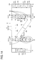
FIG. 1 shows an insulation protector used in a connection structure for electrical storage element groups of a first embodiment, -
FIG. 2 is a plan view of electrical storage element groups on which the insulation protector ofFIG. 1 is to be mounted, -
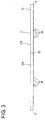
FIG. 3 is a side view of the insulation protector, -
FIG. 4 is a partial section along A-A ofFIG. 3 , -
FIG. 5 is a plan view of the electrical storage element groups on which the insulation protector ofFIG. 6 is to be mounted, -
FIG. 6 is a partial plan view of the insulation protector to be mounted on the electrical storage element groups ofFIG. 5 , -
FIG. 7 is a plan view of the electrical storage element groups on which the insulation protector ofFIG. 8 is to be mounted, -
FIG. 8 is a partial plan view of the insulation protector to be mounted on the electrical storage element groups ofFIG. 7 , -
FIG. 9 is a plan view of the electrical storage element groups on which the insulation protector ofFIG. 10 is to be mounted, -
FIG. 10 is a partial plan view of the insulation protector to be mounted on the electrical storage element groups ofFIG. 9 , -
FIG. 11 is a plan view of an electrical storage module mounted with an insulation protector used in a connection structure for electrical storage element groups of a second embodiment, -
FIG. 12 is a plan view of the electrical storage element groups, -
FIG. 13 is a plan view of the insulation protector, and -
FIG. 14 is a bottom view of the insulation protector. - Hereinafter, a first embodiment of the present invention is described with reference to
FIGS. 1 to 10 . - A
connection structure 10 for electricalstorage element groups 12 of this embodiment is such that a plurality of (two in this embodiment) electricalstorage element groups 12 are connected side by side as shown inFIG. 2 . As shown inFIG. 1 , theconnection structure 10 for the electricalstorage element groups 12 includes a first connecting member 20 (an example of a connecting member) for connecting the adjacent electricalstorage element groups 12, second connectingmembers 25 for connecting betweenelectrical storage elements storage element groups 12 and aninsulation protector 31 having a second holding portion 36 (an example of a holding portion) for holding the first connectingmember 20. An electrical storage module (not shown) formed by connecting the plurality of electricalstorage element groups 12 is used, for example, as a drive source of a vehicle such as an electric vehicle or a hybrid vehicle. - As shown in
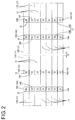
FIG. 2 , each electricalstorage element group 12 is formed by connecting a plurality of (seven in this embodiment)electrical storage elements 13 in series, eachelectrical storage element 13 including positive andnegative electrode terminals 14 on anelectrode forming surface 17A (an example of the same surface) of amain body portion 17. In each electricalstorage element group 12, theelectrical storage elements FIG. 2 are so arranged that the polarities of theelectrode terminals - The adjacent two electrical storage element groups 12 (12A, 12B) are so arranged that an
input terminal 15A and anoutput terminal 15B are diagonal to each other. Out of theelectrode terminals 14 of the two electricalstorage element groups 12, theelectrode terminal 14 on a left upper end part of the left electrical storage element group (first electricalstorage element group 12A) inFIG. 2 is theinput terminal 15A and theelectrode terminal 14 on a shown right lower end part of the right electrical storage element group (second electricalstorage element group 12B) is theoutput terminal 15B. - In this embodiment, the
electrode terminal 14 arranged on a shown lower end part (an example of one end part) of the first electricalstorage element group 12A (an example of one electrical storage element group) and on the side of the second electricalstorage element group 12B (on the side of the adjacent other electrical storage element group) is afirst electrode terminal 16A. Theelectrode terminal 14 arranged on a shown upper end part (an example of another end part opposite to the one end part of the first electricalstorage element group 12A) of the second electricalstorage element group 12B (an example of the other electrical storage element group) and on the side of the first electricalstorage element group 12A (on the side of the adjacent one electrical storage element group) is asecond electrode terminal 16B. - The
electrical storage element 13 includes the electrode terminals 14 (positive electrode terminal 14 is denoted by 14A andnegative electrode terminal 14 is denoted by 14B) perpendicularly projecting from themain body portion 17 in the form of a flat rectangular parallelepiped containing unillustrated electrical storage constituents inside. The positive andnegative electrode terminals electrical storage element 13 is rectangular tube nuts andcircular screw holes 18 are formed to penetrate therethrough. Theinsulation protector 31 is fixed by aligning throughholes 26 of the second connectingmembers 25 with thescrew holes 18 of these nuts and threadably engaging shaft parts of bolts (not shown) with these aligned holes. - The second connecting
member 25 is made of metal such as copper, copper alloy, stainless steel (SUS) or aluminum and in the form of a plate having a length corresponding to a dimension between theelectrode terminals holes 26, through which the shaft parts of the bolts (not shown) are inserted, are formed to penetrate through the second connectingmember 25. These throughholes 26 have an elliptical shape long in a lateral direction. - The first connecting
member 20 is made of metal such as copper, copper alloy, stainless steel (SUS) or aluminum. The first connectingmember 20 includes aterminal connecting portion 21 to be connected to thefirst electrode terminal 16A arranged on a left lower end part inFIG. 1 and aterminal connecting portion 21 to be connected to thesecond electrode terminal 16B arranged on a shown right upper end part. - Through
holes 22, through which the shaft parts of the bolts are inserted, are formed to penetrate through theterminal connecting portions 21. The through holes 22 of the first connectingmember 21 are set to be larger than the throughholes 26 of the second connectingmembers 25 and capable of accommodating tolerances. A part linking the twoterminal connecting portions 21 of the first connectingmember 20 is a linkingportion 23. The linkingportion 23 is formed with lockingportions 24 to be locked to the second holdingportion 36 of the insulation protector and projecting outwardly. The linkingportion 23 is arranged in an oblique direction. - The
connection structure 10 for the electricalstorage element groups 12 of this embodiment includesvoltage detection terminals 28 respectively arranged to overlap the second connectingmembers 25 and the first connectingmember 20. - The
voltage detection terminal 28 is for detecting a voltage of theelectrical storage element 13 and includes, as shown inFIG. 1 , a connectingportion 29 in the form of a flat plate formed in a central part with a penetratingcircular insertion hole 29A through which the shaft part of the bolt is insertable, and awire connecting portion 30 connected to an end part of the connectingportion 29 and to be connected to an end of a wire W. The connectingportion 29 of thevoltage detection terminal 28 is a part to be overlapped and connected to the second connectingmember 25 or the first connectingmember 20. - The
wire connecting portion 30 is crimped to a conductor exposed by stripping an insulation coating of the end of the wire W, which is a coated wire, and includes awire barrel 30A to be crimped to a conductor part of the wire W and aninsulation barrel 30B to be caulked onto the insulation coating of the wire W from above. - The wire W connected to the
voltage detection terminal 28 is drawn out from a wire draw-outportion 34 to awire holding portion 35 and guided to an unillustrated battery ECU. This battery ECU is mounted with a microcomputer, devices and the like and has a known configuration with functions of detecting voltages, currents, temperatures and the like of theelectrical storage elements 13 and executing a charge/discharge control of eachelectrical storage element 13. - The
insulation protector 31 is made of an insulating material and dividable into twounits storage element group 12 as shown inFIG. 1 . Theinsulation protector 31 is configured by coupling the twounits - Two rows of first holding
portions 33 for holding the second connectingmembers 25 connecting between theelectrical storage elements wire holding portions 35 for holding the wires W for voltage detection are provided on each of left and right end parts of theinsulation protector 31 inFIG. 1 . Further, thecoupling portions 32 for coupling the twounits member 20 connecting between the adjacent electricalstorage element groups insulation protector 31. - The
first holding portion 33 includes abottom plate 33A on which each second connectingmember 25 is to be placed and a holdingwall 33C standing up from thebottom plate 33A along the outer peripheral edge of the second connectingmembers 25. Further, a retainingprotrusion 33D for retaining the second connectingmember 25, aterminal holding portion 33E for holding thevoltage detection terminal 28 and the groove-like wire draw-outportion 34 connected to theterminal holding portion 33E and configured to draw out the wire W toward thewire holding portion 35 are provided on the inner surface of the holdingwall 33C of the first holdingportion 33. The wire draw-outportion 34 is connected to thewire holding portion 35. Parts of thebottom plate 33A into which theelectrode terminals 14 are to be inserted serve asopenings 33B where thebottom plate 33A is absent. - The holding
wall 33C is set at a height where a short circuit due to the contact of a tool or the like with the second connectingmember 25 or a head part of the bolt can be prevented. - The
wire holding portion 35 for holding the wires W connected to thevoltage detection terminals 28 is provided between the two rows of thefirst holding portions wire holding portion 35 includes abottom wall 35A on which the wires W are to be placed, and a pair ofside walls bottom wall 35A. Parts of theside walls 35B connected to the wire draw-outportions 34 are open. - The
coupling portion 32 coupling the twounits coupling protrusion 32A and acoupling receiving portion 32B for receiving thecoupling protrusion 32A, and the twounits coupling protrusion 32A of one (31A or 31 B) of theadjacent units coupling receiving portion 32B of the other unit (31B or 31A). Thecoupling protrusion 32A is movable in thecoupling receiving portion 32B in an arrangement direction of the electrical storage element groups 12 (lateral direction ofFIG. 1 ) and an arrangement direction of the electrical storage elements 13 (vertical direction ofFIG. 1 ). - The
second holding portion 36 for holding the first connectingmember 20 includes abottom plate 36A on which the first connectingmember 20 is to be placed, and aprotection wall 36C standing up from thebottom plate 36A along the outer peripheral edge of the first connectingmember 20. A part of theprotection wall 36C where one end part (end part arranged on a right upper side shown inFIG. 1 ) of the first connectingmember 20 is to be arranged is formed with aterminal holding portion 36E for holding thevoltage detection terminal 28. Parts of thebottom plate 36A where theelectrode terminals 14 are to be arranged serve asopenings 36B where thebottom plate 36A is absent. Theprotection wall 36C is set at a height where a short circuit due to the contact of the tool or the like with the first connectingmember 20 or the head part of the bolt can be prevented. - Retaining
protrusions 36D for retaining the first connectingmember 20 are provided on the inner surface of theprotection wall 36C. Further, theprotection wall 36C is formed with lockedportions 37 to which the lockingportions 24 of the first connectingmember 20 are to be locked. Clearances C1 are provided between theprotection wall 36C and the linkingportion 23 of the first connectingmember 20 so that the first connectingmember 20 moves in the second holdingportion 36 to accommodate a displacement between thefirst electrode terminal 16A and theterminal connecting portion 21 and that between thesecond electrode terminal 16B and theterminal connecting portion 21 in the arrangement direction of theelectrical storage elements 13 and the arrangement direction of the electrical storage element groups 12. - Further, clearances C2 are also provided between the
protection wall 36C and endparts 21A of theterminal connecting portions 21 of the first connectingmember 20 to be able to accommodate the displacement between thefirst end part 16A and theterminal connecting portion 21 and that between thesecond electrode terminal 16B and theterminal connecting portion 21 in the arrangement direction of the electrical storage element groups 12. - As shown in
FIG. 3 ,positioning portions 38 projecting downwardly and to be positioned with respect to the electricalstorage element groups 12 by being fitted into the nuts of theelectrical storage elements 13 are provided on the underside of theinsulation protector 31. As shown inFIG. 4 , thepositioning portions 38 are formed on the undersides of the first and fourth first holdingportions 33 from top. - Next, a connection method of the electrical
storage element groups 12 is described. - As shown in
FIG. 2 , two electrical storage element groups 12 (12A, 12B) in each of which sevenelectrical storage elements 13 are so arranged that theadjacent electrode terminals - Subsequently, the
voltage detection terminals 28 connected to the wires W are placed on the second connectingmembers 25 and the first connectingmember 20 and this assembly is accommodated into thefirst holding portions 33 and the second holdingportion 36 of the insulation protector 31 (this is a wiring module 11). - Subsequently, the
wiring module 11 is mounted on surfaces of the two electricalstorage element groups electrode terminals 14 are arranged. When thewiring module 11 is mounted on the electricalstorage element groups 12, the nuts of theelectrode terminals 14 are fitted into thepositioning portions 38 of theinsulation protector 31 to position theinsulation protector 31 and eachterminal connecting portion 21 of the first connectingmember 20 is positioned with respect to the electrical storage element groups 12. - Here, if the adjacent two electrical
storage element groups FIG. 2 , there is almost no tolerance between the two electricalstorage element groups right units wiring module 11 mounted on the electricalstorage element groups 12 are hardly displaced (seeFIG. 1 ). X1 inFIG. 2 denotes an interval between the adjacent electrical storage element groups 12. Cases where the two electricalstorage element groups storage element groups FIG. 2 are described below. - There are cases where, as shown in
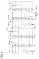
FIG. 5 , the second electricalstorage element group 12B is projecting more (upwardly inFIG. 5 ) than the first electricalstorage element group 12A although an interval X2 between the adjacent two electricalstorage element groups storage element groups FIG. 2 . Y2 inFIG. 5 denotes a projecting distance and Z2 inFIG. 6 denotes an interval between theunits - Even in cases as shown in
FIG. 5 , the clearances C2 are set between the linkingportion 23 of the first connectingmember 20 and theprotection wall 36C and between theend parts 21A of theterminal connecting portions 21 of the first connectingmember 20 and theprotection wall 36C in this embodiment. Thus, the first connectingmember 20 is movable in the second holdingportion 36 in both the arrangement direction of the electricalstorage element groups 12 and that of theelectrical storage elements 13. In cases as shown inFIG. 5 , thewiring module 11 is mounted such that theright unit 31B is displaced upwardly with respect to theleft unit 31A as shown inFIG. 6 , and the connectingmember 20 moves in the second holdingportion 36 of theinsulation protector 31. - There are cases where, as shown in
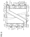
FIG. 7 , an interval X3 between the adjacent two electricalstorage element groups storage element groups FIG. 2 and the second electricalstorage element group 12B is projecting more (upwardly inFIG. 7 ) than the first electricalstorage element group 12A. Y3 inFIG. 7 denotes a projecting distance and Z3 inFIG. 8 denotes an interval between theunits - Even in cases as shown in
FIG. 7 , the first connectingmember 20 is movable in the second holdingportion 36 in both the arrangement direction of the electricalstorage element groups 12 and that of theelectrical storage elements 13 as in cases as shown inFIG. 5 . In cases as shown inFIG. 7 , thewiring module 11 is mounted such that theright unit 31B is displaced upwardly with respect to theleft unit 31A and the interval Z3 between theunits FIG. 8 , and the connectingmember 20 moves in the second holdingportion 36 of theinsulation protector 31. - There are cases where, as shown in
FIG. 9 , the first electricalstorage element group 12A is projecting more (upwardly inFIG. 9 ) than the second electricalstorage element group 12B although an interval X4 between the adjacent two electricalstorage element groups storage element groups FIG. 2 . Y4 inFIG. 9 denotes a projecting distance and Z4 inFIG. 10 denotes an interval between theunits - Even in cases as shown in
FIG. 9 , the first connectingmember 20 is movable in the second holdingportion 36 in both the arrangement direction of the electricalstorage element groups 12 and that of theelectrical storage elements 13. In cases as shown inFIG. 9 , thewiring module 11 is mounted such that theleft unit 31A is displaced upwardly with respect to theright unit 31 B as shown inFIG. 10 , and the connectingmember 20 moves in the second holdingportion 36 of theinsulation protector 31. - Since the locking
portions 24 of the first connectingmember 20 are locked to the lockedportions 37 of the second holdingportion 36 regardless of which one of the arranged states ofFIGS. 2 ,5 ,7 and9 the arranged state of the two electricalstorage element groups members 20 can be suppressed. - If the
wiring module 11 is fixed to the electricalstorage element groups 12 by being bolted to eachelectrode terminal 14 after being mounted in this way, the electrical storage module in a state where theelectrical storage elements 13 can be electrically connected by the second connectingmembers 25 and the two electricalstorage element groups member 20 is obtained. - According to the above embodiment, the following effects are exhibited.
- In this embodiment, the adjacent electrical
storage element groups member 20 for connecting thefirst electrode terminal 16A that is theelectrode terminal 14 arranged on one end part of one 12A of the adjacent electricalstorage element groups 12 and on the side of the adjacent other electricalstorage element group 12B, and thesecond electrode terminal 16B that is theelectrode terminal 14 arranged on the other end part of the other electricalstorage element group 12B opposite to the one end part of the one electricalstorage element group 12A and on the side of the adjacent one electricalstorage element group 12A. - That is, in this embodiment, the adjacent two electrical
storage element groups member 20 regardless of the number of theelectrical storage elements 13 constituting the electrical storage element groups 12. Thus, weight saving is possible and a material for fabricating an electrically connecting member can be reduced. As a result, according to this embodiment, it is possible to provide theconnection structure 10 for the electricalstorage element groups 12 reduced in cost and weight. - Further, according to this embodiment, the
insulation protector 31 is dividable into units for each electricalstorage element group 12, and the clearances C1 are provided between theprotection wall 36C of the second holdingportion 36 of theinsulation protector 31 and the linkingportion 23 of the first connectingmember 20. Thus, the first connectingmember 20 can move in the second holdingportion 36 to be able to accommodate the displacement between thefirst electrode terminal 16A and theterminal connecting portion 21 and that between thesecond electrode terminal 16B and theterminal connecting portion 21 in the arrangement direction of theelectrical storage elements storage element groups - Further, according to this embodiment, since the clearances C2 are provided between the
end parts 21A of theterminal connecting portions 21 of the first connectingmember 20 and theprotection wall 36C, the displacement between thefirst electrode terminal 16A and theterminal connecting portion 21 and that between thesecond electrode terminal 16B and theterminal connecting portion 21 in the arrangement direction of the electricalstorage element groups - Further, according to this embodiment, since the
insulation protector 31 includes thepositioning portions 38 to be positioned with respect to the electricalstorage element groups 12, an operation of mounting theinsulation protector 31 on the electricalstorage element groups 12 is easily performed. - Furthermore, according to this embodiment, since the linking
portion 23 of the first connectingmember 20 is provided with the lockingportions 24 to be locked to the second holdingportion 36 of theinsulation protector 31, excessive movements of the first connectingmember 20 can be suppressed. - Hereinafter, a second embodiment of the present invention is described with reference to
FIGS. 11 to 14 . Components similar to those of the first embodiment are denoted by the same reference signs and repeated description is omitted. - This embodiment differs from the first embodiment in that a left electrical storage element group (an example of one electrical storage element group, referred to as a first electrical
storage element group 42A) inFIG. 11 is electrically connected also to a shown right upper electrical storage element (third electrical storage element 43) (seeFIG. 11 ). - A connection structure 40 for electrical storage element groups of this embodiment includes, as shown in
FIG. 11 , a first connecting member 50 (an example of a connecting member) for connecting two adjacent electricalstorage element groups 42, second connectingmembers 25 for connecting betweenelectrical storage elements storage element groups 42 and aninsulation protector 61 having a second holding portion 66 (an example of a holding portion) for holding the first connectingmember 50. In this embodiment, the connection structure 40 further includes a third connectingmember 54 for electrically connecting the first electricalstorage element group 42A and the thirdelectrical storage element 43. - As shown in
FIG. 11 , the first electricalstorage element group 42A is formed by connecting fourelectrical storage elements 13 in series, eachelectrical storage element 13 having positive andnegative electrode terminals 14 on anelectrode forming surface 17A of amain body portion 17. As shown inFIG. 11 , the second electricalstorage element group 42B is formed by connecting threeelectrical storage elements 13 in series, eachelectrical storage element 13 having positive andnegative electrode terminals 14 on anelectrode forming surface 17A of amain body portion 17. In each electricalstorage element group 42, theelectrical storage elements FIG. 11 are so arranged that the polarities of theelectrode terminals - The
electrode terminal 14 on a lower end part of a right side of the second electricalstorage element group 42B out of theelectrode terminals 14 of the two electrical storage element groups 42 (42A, 42B) is aninput terminal 45A and theelectrode terminal 14 on a shown right side of the thirdelectrical storage element 43 is an output terminal 45B. - In this embodiment, the
electrode terminal 14 arranged on a shown lower end part of the first electricalstorage element group 42A (an example of one end part of one electrical storage element group) and on the side of the second electricalstorage element group 42B is afirst electrode terminal 46A. Theelectrode terminal 14 arranged on a shown upper end part (another end part opposite to the end part) of the second electricalstorage element group 42B and on the side of the first electricalstorage element group 42A (on the side of the adjacent one electricalstorage element group 42A) is asecond electrode terminal 46B. - In this embodiment, the first connecting
member 50 is made of metal such as copper, copper alloy, stainless steel (SUS) or aluminum. The first connectingmember 50 includes aterminal connecting portion 51 to be connected to thefirst electrode terminal 46A on a left lower side inFIG. 11 and aterminal connecting portion 51 to be connected to thesecond end part 46B on a shown right upper end part. A part of the first connectingmember 50 linking the twoterminal connecting portions 51 is a linkingportion 53. The linkingportion 53 is arranged in an oblique direction. - Through
holes 52, through which shaft parts of bolts are to be inserted, are formed to penetrate through theterminal connecting portions 51. The through holes 52 of the first connectingmember 50 are set to be larger than throughholes 26 of second connectingmembers 25 and capable of accommodating tolerances. The linkingportion 53 of the first connectingmember 50 of this embodiment is not provided with any structure to be locked to theinsulation protector 61. The configuration of the second connectingmembers 25 is as in the first embodiment. - The third connecting
member 54 is a rectangular connecting member made of metal such as copper, copper alloy, stainless steel (SUS) or aluminum. The third connectingmember 54 has a length corresponding to a dimension between the right electrode terminal of the first electricalstorage element group 42A and theleft electrode terminal 14 of the thirdelectrical storage element 43 and is formed with a pair of throughholes 56 through which shaft parts of bolts (not shown) are to be inserted. These throughholes 56 have an elliptical shape long in the lateral direction. - The
insulation protector 61 is made of an insulating material and dividable into twounits storage element group 42 as shown inFIG. 11 . Theinsulation protector 61 is configured by coupling the twounits coupling portions 65 provided on athird holding portion 64. Thesecond holding portion 66 and the third holdingportion 64 are formed by coupling the twounits - Two rows of first holding
portions 63 for holding the second connectingmembers 25 connecting between theelectrical storage elements insulation protector 61 inFIG. 11 . Further, the third holdingportion 64 for holding the third connectingmember 54 and the second holdingportion 66 for holding the first connectingmember 50 are provided substantially in the center of theinsulation protector 61. - The
first holding portion 63 includes abottom plate 63A on which each second connectingmember 25 is to be placed, and a holdingwall 63C standing up from thebottom plate 63A along the outer peripheral edge of the second connectingmembers 25. Further, a retainingprotrusion 63D for retaining the second connectingmember 25 is provided on the inner surface of the holdingwall 63C of the first holdingportion 63. Parts of thebottom plate 63A into which theelectrode terminals 14 are to be inserted serve asopenings 63B where thebottom plate 63A is absent. Aprotection wall 64C is set at a height where a short circuit due to the contact of a tool or the like with the second connectingmember 25 or a head part of the bolt can be prevented. - The
second holding portion 66 includes abottom plate 66A on which the first connectingmember 50 is to be placed, and aprotection wall 66C standing up from thebottom plate 66A along the outer peripheral edge of the first connectingmember 50. Parts of thebottom plate 66A where theelectrode terminals 14 are to be arranged serve asopenings 66B where thebottom plate 66A is absent. Theprotection wall 66C is set at a height where a short circuit due to the contact of the tool or the like with the first connectingmember 50 or the head part of the bolt can be prevented. - Retaining
protrusions 66D for retaining the first connectingmember 50 are provided on the inner surface of theprotection wall 66C. Clearances C3 are provided between theprotection wall 66C and the linkingportion 53 of the first connectingmember 50 so that the first connectingmember 50 moves in the second holdingportion 66 to accommodate a displacement between thefirst electrode terminal 46A and theterminal connecting portion 51 and that between thesecond electrode terminal 46B and theterminal connecting portion 51 in an arrangement direction of theelectrical storage elements 13 and an arrangement direction of the electrical storage element groups 42. - Further, clearances C4 are provided also between the
protection wall 66C and endparts 51A of theterminal connecting portions 51 of the first connectingmember 50 to be able to accommodate the displacement between thefirst end part 46A and theterminal connecting portion 51 and that between thesecond electrode terminal 46B and theterminal connecting portion 51 in the arrangement direction of the electrical storage element groups 42. - The
third holding portion 64 for holding the third connectingmember 54 includes abottom plate 64A on which the third connectingmember 54 is to be placed, and aprotection wall 64C standing up from thebottom plate 64A along the outer peripheral edge of the third connectingmember 54. Parts of thebottom plate 64A where theelectrode terminals 14 are to be arranged serve asopenings 64B where thebottom plate 64A is absent. Theprotection wall 64C is set at a height where a short circuit due to the contact of the tool or the like with the third connectingmember 54 or the head part of the bolt can be prevented. Retainingprotrusions 64D for retaining the third connectingmember 54 are provided on the inner surface of theprotection wall 64C. Clearances C5 are provided also between theprotection wall 64C and endparts 55A of terminal connectingportions 55 of the third connectingmember 54 to be able to accommodate a displacement between theelectrode terminal 14 of the thirdelectrical storage element 43 and theterminal connecting portion 55 and that between theelectrode terminal 14 of the first electricalstorage element group 42B and theterminal connecting portion 55 in the arrangement direction of theelectrical storage elements 42. - The
third holding portion 64 is provided with thecoupling portions 65 for coupling the twounits coupling portion 65 is composed of acoupling protrusion 65A and acoupling receiving portion 65B for receiving thecoupling protrusion 65A, and theunits coupling protrusion 65A of one 61A or 61B of theadjacent units coupling receiving portion 65B of theother unit coupling protrusion 65A is movable in thecoupling receiving portion 65B in the arrangement direction of the electrical storage element groups 42 (lateral direction ofFIG. 11 ). - As shown in
FIG. 13 ,positioning portions 68 projecting downwardly and to be positioned with respect to the electricalstorage element groups 42 by being fitted into nuts of theelectrical storage elements 13 are provided on the underside of theinsulation protector 61. As shown inFIG. 14 , thepositioning portions 68 are formed on the underside of thethird holding portions 63 from top. - Next, a connection method of the electrical
storage element groups 42 is described. - As shown in
FIG. 12 , the first electricalstorage element group 42A in which fourelectrical storage elements 13 are so arranged that theadjacent electrode terminals storage element group 42B in which threeelectrical storage elements 13 are so arranged that theadjacent electrode terminals electrical storage element 43 is arranged above the second electricalstorage element group 42B as shown. - By coupling the two
units insulation protector 61 formed with the second holdingportion 66 and the third holdingportion 64 is obtained. By accommodating the first connectingmember 50 into the second holdingportion 66 of thisinsulation protector 61, the second connectingmembers 25 into thefirst holding portions 63 and the third connectingmember 54 into the third holdingportion 64, awiring module 41 is obtained. If necessary, voltage detection terminals (not shown) connected to wires may be placed on predetermined connecting member(s) and accommodated in predetermined holding portions of theinsulation protector 61. Voltage detection terminals configured as illustrated in the first embodiment may be used. - Subsequently, the
wiring module 41 is mounted on surfaces of the two electricalstorage element groups electrical storage element 43 where theelectrode terminals 14 are arranged. When thewiring module 41 is mounted on the electricalstorage element groups 42 and the thirdelectrical storage element 43, the nuts of theelectrode terminals 14 are fitted into thepositioning portions 68 of theinsulation protector 61 to position theinsulation protector 61 and eachterminal connecting portion 51 of the first connectingmember 50 is positioned on the electrical storage element groups 42. - Here, if there is almost no tolerance between the two electrical
storage element groups electrical storage elements 13, thewiring module 41 is mounted on the electricalstorage element groups 42 without any problem. Even if there is any deviation in the interval between the electricalstorage element groups 42 or any displacement in the arrangement direction, the first connectingmember 50 is movable in the second holdingportion 66 in both the arrangement direction of the electricalstorage element groups 42 and that of theelectrical storage elements 13 since the clearances C3 are set between the linkingportion 53 of the first connectingmember 50 and theprotection wall 66C and the clearances C4 are set between theend parts 51A of theterminal connecting portions 51 of the first connectingmember 50 and theprotection wall 66C. - If the
wiring module 41 is fixed to the electricalstorage element groups 42 and the thirdelectrical storage element 43 by being bolted to eachelectrode terminal 14 after being mounted in this way, an electrical storage module M in a state where theelectrical storage elements 13 can be electrically connected by the second connectingmembers 25, the two electricalstorage element groups member 50 and the first electricalstorage element group 42A and the thirdelectrical storage element 43 can be electrically connected by the third connectingmember 54 is obtained. - Also in this embodiment, the adjacent two electrical
storage element groups member 50 regardless of the number of theelectrical storage elements 13 constituting the electricalstorage element groups 42 as in the first embodiment. Thus, weight saving is possible and a material for fabricating an electrically connecting member can be reduced. As a result, according to this embodiment, it is possible to provide the connection structure 40 for electrical storage element groups reduced in cost and weight. - Further, the following effects are obtained also by this embodiment.
- According to this embodiment, the
insulation protector 61 is dividable for each electricalstorage element group 42, and the clearances C3 are provided between theprotection wall 66C of the second holdingportion 66 of theinsulation protector 61 and the linkingportion 53 of the first connectingmember 50. Thus, the first connectingmember 50 can move in the second holdingportion 66 to be able to accommodate the displacement between thefirst electrode terminal 46A and theterminal connecting portion 51 and that between thesecond electrode terminal 46B and theterminal connecting portion 51 in the arrangement direction of theelectrical storage elements - According to this embodiment, since the clearances C4 are provided between the
end parts 51A of theterminal connecting portions 51 of the first connectingmember 50 and theprotection wall 66C, the displacement between thefirst electrode terminal 46A and theterminal connecting portion 51 and that between thesecond electrode terminal 46B and theterminal connecting portion 51 in the arrangement direction of the electricalstorage element groups 42 can be accommodated. - According to this embodiment, since the
insulation protector 61 includes thepositioning portions 68 to be positioned with respect to the electricalstorage element groups 42, an operation of mounting theinsulation protector 61 on the electricalstorage element groups 42 is easily performed. - The present invention is not limited to the above described and illustrated embodiments. For example, the following embodiments are also included in the technical scope of the present invention.
- (1) Although the
insulation protector 31 dividable for each electricalstorage element group 12 is illustrated in the above embodiments, an integrated insulation protector may be used. - (2) Although the clearances C1, C2 provided between the linking
portion 23 of the first connectingmember 20 and theprotection wall 36C and between theend parts 21A of theterminal connecting portions 21 of the first connectingmember 20 and theprotection wall 36C are illustrated in the above embodiments, only either one of them may be provided. - (3) Although the
insulation protector 31 including thepositioning portions 38 to be positioned with respect to the electricalstorage element groups 12 is illustrated in the above embodiments, the positioning portions may not be provided. - (4) Although the electrical storage module formed by connecting two electrical
storage element groups 42 and one electrical storage element 13 (third electrical storage element 43) is shown in the second embodiment, an electrical storage element group composed of a plurality of electrical storage elements may be connected to two electrical storage element groups instead of oneelectrical storage element 13. Further, four or more electrical storage element groups may be connected. -
- 10, 40 ....
- connection structure for electrical storage element groups
- 11, 41 ...
- wiring module
- 12, 42 ...
- electrical storage element group
- 12A, 42A ...
- first electrical storage element group (one electrical storage element group)
- 12B, 42B ...
- second electrical storage element group (other electrical storage element group)
- 13 ...
- electrical storage element
- 14 ...
- electrode terminal
- 14A ...
- positive electrode terminal
- 14B c
- negative electrode terminal
- 15A, 45A ...
- input terminal
- 15B, 45B ...
- output terminal
- 16A, 46A ...
- first electrode terminal
- 16B, 46B ...
- second electrode terminal
- 20, 50 ...
- first connecting member (connecting member)
- 21, 51 ...
- terminal connecting portion
- 21A, 51A ...
- end part (of terminal connecting portion)
- 23, 53 ...
- linking portion
- 24 ...
- locking portion
- 31, 61 ...
- insulation protector
- 31A, 61A ...
- (left) unit
- 31B, 61B ...
- (right) unit
- 36, 66 ...
- second holding portion
- 36A, 66A ...
- bottom plate
- 36C, 66C ...
- protection wall
- 36E ...
- terminal holding portion
- 37 ...
- locked portion
- 38, 68...
- positioning portion
- C1, C3 ...
- clearance (between linking portion and protection wall)
- C2, C4 ...
- clearance (between end part of terminal connecting portion and protection wall)
Claims (5)
- A connection structure for electrical storage element groups for connecting a plurality of electrical storage element groups side by side, each electrical storage element group being formed by connecting a plurality of electrical storage elements each having positive and negative electrode terminals on the same surface in series, wherein:the plurality of electrical storage element groups are electrically connected by connecting a connecting member for connecting adjacent ones of the electrical storage element groups to a first electrode terminal and a second electrode terminal, the first electrode terminal being the electrode terminal arranged on one end part of one electrical storage element group and on the side of the adjacent other electrical storage element group and the second electrode terminal being the electrode terminal arranged on another end part of the other electrical storage element group opposite to the one end part of the one electrical storage element group and on the side of the adjacent one electrical storage element group.
- A connection structure for electrical storage element groups according to claim 1, further comprising an insulation protector made of an insulating material, including a holding portion for holding the connecting member and dividable for each of the electrical storage element groups, wherein:the connecting member includes two terminal connecting portions to be respectively connected to the first and second electrode terminals and a linking portion linking the two terminal connecting portions, whereas the holding portion of the insulation protector includes a protection wall arranged along a peripheral edge of the connecting member; anda clearance is provided between the linking portion of the connecting member and the protection wall.
- A connection structure for electrical storage element groups according to claim 2, wherein a clearance is provided between an end part of the terminal connecting portion of the connecting member and the protection wall.
- A connection structure for electrical storage element groups according to claim 2 or 3, wherein the insulation protector includes a positioning portion to be positioned with respect to the electrical storage element groups.
- A connection structure for electrical storage element groups according to any one of claims 2 to 4, wherein the linking portion of the connecting member includes a locking portion to be locked to the holding portion of the insulation protector.
Applications Claiming Priority (2)
| Application Number | Priority Date | Filing Date | Title |
|---|---|---|---|
| JP2013241754 | 2013-11-22 | ||
| PCT/JP2014/077160 WO2015076034A1 (en) | 2013-11-22 | 2014-10-10 | Connection structure for electrical storage element group |
Publications (3)
| Publication Number | Publication Date |
|---|---|
| EP3073550A1 true EP3073550A1 (en) | 2016-09-28 |
| EP3073550A4 EP3073550A4 (en) | 2017-01-25 |
| EP3073550B1 EP3073550B1 (en) | 2018-03-14 |
Family
ID=53179304
Family Applications (1)
| Application Number | Title | Priority Date | Filing Date |
|---|---|---|---|
| EP14864034.5A Not-in-force EP3073550B1 (en) | 2013-11-22 | 2014-10-10 | Connection structure for electrical storage element group |
Country Status (5)
| Country | Link |
|---|---|
| US (1) | US10297806B2 (en) |
| EP (1) | EP3073550B1 (en) |
| JP (1) | JP6052427B2 (en) |
| CN (1) | CN106104853B (en) |
| WO (1) | WO2015076034A1 (en) |
Families Citing this family (8)
| Publication number | Priority date | Publication date | Assignee | Title |
|---|---|---|---|---|
| DE102016121265B4 (en) * | 2016-11-07 | 2025-08-07 | Elringklinger Ag | Cell contact system for an electrochemical device |
| JP6629710B2 (en) * | 2016-11-08 | 2020-01-15 | トヨタ自動車株式会社 | Battery pack |
| JP6790923B2 (en) * | 2017-03-03 | 2020-11-25 | 株式会社オートネットワーク技術研究所 | Connection module |
| JP6350721B1 (en) * | 2017-06-12 | 2018-07-04 | 株式会社オートネットワーク技術研究所 | External connection busbar holding module, connection module and power storage module |
| JP6414361B1 (en) * | 2018-03-30 | 2018-10-31 | 株式会社オートネットワーク技術研究所 | Connection module |
| CN111384347B (en) * | 2018-12-29 | 2022-08-30 | 东莞莫仕连接器有限公司 | Battery connection module |
| JP7147701B2 (en) * | 2019-07-05 | 2022-10-05 | 株式会社オートネットワーク技術研究所 | Battery pack and external connection module system |
| EP4195353A1 (en) * | 2021-12-13 | 2023-06-14 | Volvo Car Corporation | Battery cell assembly and battery unit for an electric vehicle |
Family Cites Families (13)
| Publication number | Priority date | Publication date | Assignee | Title |
|---|---|---|---|---|
| KR100889241B1 (en) | 2006-10-23 | 2009-03-17 | 주식회사 엘지화학 | Electrode terminal connection member of battery module |
| JP2009087720A (en) | 2007-09-28 | 2009-04-23 | Toshiba Corp | Battery pack |
| US8403091B2 (en) | 2009-04-22 | 2013-03-26 | Amit Prakash | Pneumatic-IC engine based power management system for automobiles and the like |
| JP5504979B2 (en) * | 2010-03-03 | 2014-05-28 | 株式会社オートネットワーク技術研究所 | Battery connection assembly |
| JP5396366B2 (en) | 2010-10-13 | 2014-01-22 | 大東電機工業株式会社 | Massage equipment |
| JP2012099355A (en) * | 2010-11-02 | 2012-05-24 | Sumitomo Wiring Syst Ltd | Battery module and battery connection configuration |
| CN103238232A (en) * | 2010-11-30 | 2013-08-07 | 松下电器产业株式会社 | Battery module and battery pack |
| US8632905B2 (en) | 2010-12-13 | 2014-01-21 | Panasonic Corporation | Battery module and battery pack |
| JP5418522B2 (en) * | 2011-03-07 | 2014-02-19 | 株式会社オートネットワーク技術研究所 | Battery connection assembly and battery module |
| JP5803405B2 (en) | 2011-08-10 | 2015-11-04 | 株式会社オートネットワーク技術研究所 | Bus bar cover and bus bar with cover |
| JP5145452B1 (en) | 2011-09-16 | 2013-02-20 | 日本航空電子工業株式会社 | Power storage device |
| JP2013077500A (en) * | 2011-09-30 | 2013-04-25 | Lithium Energy Japan:Kk | Battery pack |
| JP2013187046A (en) * | 2012-03-08 | 2013-09-19 | Nissan Motor Co Ltd | Battery pack |
-
2014
- 2014-10-10 US US15/037,082 patent/US10297806B2/en not_active Expired - Fee Related
- 2014-10-10 CN CN201480062658.3A patent/CN106104853B/en not_active Expired - Fee Related
- 2014-10-10 EP EP14864034.5A patent/EP3073550B1/en not_active Not-in-force
- 2014-10-10 WO PCT/JP2014/077160 patent/WO2015076034A1/en not_active Ceased
- 2014-10-10 JP JP2015549031A patent/JP6052427B2/en not_active Expired - Fee Related
Also Published As
| Publication number | Publication date |
|---|---|
| JPWO2015076034A1 (en) | 2017-03-16 |
| EP3073550B1 (en) | 2018-03-14 |
| WO2015076034A1 (en) | 2015-05-28 |
| EP3073550A4 (en) | 2017-01-25 |
| US20160293925A1 (en) | 2016-10-06 |
| CN106104853B (en) | 2019-03-15 |
| US10297806B2 (en) | 2019-05-21 |
| JP6052427B2 (en) | 2016-12-27 |
| CN106104853A (en) | 2016-11-09 |
Similar Documents
| Publication | Publication Date | Title |
|---|---|---|
| EP3073550B1 (en) | Connection structure for electrical storage element group | |
| EP2772961B1 (en) | Battery module | |
| US9780351B2 (en) | Wiring module | |
| EP3136470B1 (en) | Wiring module, wiring-module intermediary body, and method for manufacturing wiring module | |
| EP2674998B1 (en) | Bus bar module | |
| US11139536B2 (en) | Connection module | |
| EP2688122A1 (en) | Wiring module | |
| US9905832B2 (en) | Battery wiring module | |
| JP6579030B2 (en) | Connection module | |
| CN106471647B (en) | Motor vehicle batteries that can be manufactured with voltage protection | |
| EP2908362B1 (en) | Wiring module | |
| US20170294640A1 (en) | Wiring module and method for producing wiring module | |
| JP2013150526A (en) | Power converter | |
| CN106797009B (en) | Wiring module and power storage module | |
| CN108780872A (en) | Battery and method for manufacturing battery | |
| EP3496179B1 (en) | Connector for a battery pack | |
| CN112534632A (en) | Battery case, battery system, and mounting method for battery system | |
| US20180122574A1 (en) | Power storage module | |
| EP2879255A1 (en) | Electrical connection box | |
| EP3136472A1 (en) | Wiring module | |
| US10084210B2 (en) | Electrochemical cell module | |
| JP2016201179A (en) | Power storage module | |
| EP2892089B1 (en) | Electric wire routing structure for bus bar module | |
| EP3116045B1 (en) | Electricity storage module | |
| JP2016225231A (en) | Battery pack |
Legal Events
| Date | Code | Title | Description |
|---|---|---|---|
| PUAI | Public reference made under article 153(3) epc to a published international application that has entered the european phase |
Free format text: ORIGINAL CODE: 0009012 |
|
| 17P | Request for examination filed |
Effective date: 20160428 |
|
| AK | Designated contracting states |
Kind code of ref document: A1 Designated state(s): AL AT BE BG CH CY CZ DE DK EE ES FI FR GB GR HR HU IE IS IT LI LT LU LV MC MK MT NL NO PL PT RO RS SE SI SK SM TR |
|
| AX | Request for extension of the european patent |
Extension state: BA ME |
|
| A4 | Supplementary search report drawn up and despatched |
Effective date: 20161223 |
|
| RIC1 | Information provided on ipc code assigned before grant |
Ipc: H01M 2/10 20060101ALI20161219BHEP Ipc: H01G 11/76 20130101ALI20161219BHEP Ipc: H01G 2/04 20060101ALN20161219BHEP Ipc: H01G 11/10 20130101ALI20161219BHEP Ipc: H01M 2/34 20060101ALI20161219BHEP Ipc: H01M 2/20 20060101AFI20161219BHEP |
|
| DAX | Request for extension of the european patent (deleted) | ||
| GRAP | Despatch of communication of intention to grant a patent |
Free format text: ORIGINAL CODE: EPIDOSNIGR1 |
|
| STAA | Information on the status of an ep patent application or granted ep patent |
Free format text: STATUS: GRANT OF PATENT IS INTENDED |
|
| RIC1 | Information provided on ipc code assigned before grant |
Ipc: H01M 2/10 20060101ALI20171005BHEP Ipc: H01M 2/34 20060101ALI20171005BHEP Ipc: H01G 11/76 20130101ALI20171005BHEP Ipc: H01G 2/04 20060101ALN20171005BHEP Ipc: H01G 11/10 20130101ALI20171005BHEP Ipc: H01M 2/20 20060101AFI20171005BHEP |
|
| RIC1 | Information provided on ipc code assigned before grant |
Ipc: H01M 2/10 20060101ALI20171006BHEP Ipc: H01M 2/20 20060101AFI20171006BHEP Ipc: H01M 2/34 20060101ALI20171006BHEP Ipc: H01G 2/04 20060101ALN20171006BHEP Ipc: H01G 11/76 20130101ALI20171006BHEP Ipc: H01G 11/10 20130101ALI20171006BHEP |
|
| INTG | Intention to grant announced |
Effective date: 20171026 |
|
| RAP1 | Party data changed (applicant data changed or rights of an application transferred) |
Owner name: SUMITOMO ELECTRIC INDUSTRIES, LTD. Owner name: SUMITOMO WIRING SYSTEMS, LTD. Owner name: AUTONETWORKS TECHNOLOGIES, LTD. |
|
| GRAS | Grant fee paid |
Free format text: ORIGINAL CODE: EPIDOSNIGR3 |
|
| GRAA | (expected) grant |
Free format text: ORIGINAL CODE: 0009210 |
|
| STAA | Information on the status of an ep patent application or granted ep patent |
Free format text: STATUS: THE PATENT HAS BEEN GRANTED |
|
| AK | Designated contracting states |
Kind code of ref document: B1 Designated state(s): AL AT BE BG CH CY CZ DE DK EE ES FI FR GB GR HR HU IE IS IT LI LT LU LV MC MK MT NL NO PL PT RO RS SE SI SK SM TR |
|
| REG | Reference to a national code |
Ref country code: GB Ref legal event code: FG4D |
|
| REG | Reference to a national code |
Ref country code: CH Ref legal event code: EP Ref country code: AT Ref legal event code: REF Ref document number: 979678 Country of ref document: AT Kind code of ref document: T Effective date: 20180315 |
|
| REG | Reference to a national code |
Ref country code: IE Ref legal event code: FG4D |
|
| REG | Reference to a national code |
Ref country code: DE Ref legal event code: R096 Ref document number: 602014022453 Country of ref document: DE |
|
| REG | Reference to a national code |
Ref country code: NL Ref legal event code: MP Effective date: 20180314 |
|
| REG | Reference to a national code |
Ref country code: LT Ref legal event code: MG4D |
|
| PG25 | Lapsed in a contracting state [announced via postgrant information from national office to epo] |
Ref country code: FI Free format text: LAPSE BECAUSE OF FAILURE TO SUBMIT A TRANSLATION OF THE DESCRIPTION OR TO PAY THE FEE WITHIN THE PRESCRIBED TIME-LIMIT Effective date: 20180314 Ref country code: HR Free format text: LAPSE BECAUSE OF FAILURE TO SUBMIT A TRANSLATION OF THE DESCRIPTION OR TO PAY THE FEE WITHIN THE PRESCRIBED TIME-LIMIT Effective date: 20180314 Ref country code: NO Free format text: LAPSE BECAUSE OF FAILURE TO SUBMIT A TRANSLATION OF THE DESCRIPTION OR TO PAY THE FEE WITHIN THE PRESCRIBED TIME-LIMIT Effective date: 20180614 Ref country code: CY Free format text: LAPSE BECAUSE OF FAILURE TO SUBMIT A TRANSLATION OF THE DESCRIPTION OR TO PAY THE FEE WITHIN THE PRESCRIBED TIME-LIMIT Effective date: 20180314 Ref country code: LT Free format text: LAPSE BECAUSE OF FAILURE TO SUBMIT A TRANSLATION OF THE DESCRIPTION OR TO PAY THE FEE WITHIN THE PRESCRIBED TIME-LIMIT Effective date: 20180314 |
|
| REG | Reference to a national code |
Ref country code: AT Ref legal event code: MK05 Ref document number: 979678 Country of ref document: AT Kind code of ref document: T Effective date: 20180314 |
|
| PG25 | Lapsed in a contracting state [announced via postgrant information from national office to epo] |
Ref country code: GR Free format text: LAPSE BECAUSE OF FAILURE TO SUBMIT A TRANSLATION OF THE DESCRIPTION OR TO PAY THE FEE WITHIN THE PRESCRIBED TIME-LIMIT Effective date: 20180615 Ref country code: BG Free format text: LAPSE BECAUSE OF FAILURE TO SUBMIT A TRANSLATION OF THE DESCRIPTION OR TO PAY THE FEE WITHIN THE PRESCRIBED TIME-LIMIT Effective date: 20180614 Ref country code: RS Free format text: LAPSE BECAUSE OF FAILURE TO SUBMIT A TRANSLATION OF THE DESCRIPTION OR TO PAY THE FEE WITHIN THE PRESCRIBED TIME-LIMIT Effective date: 20180314 Ref country code: SE Free format text: LAPSE BECAUSE OF FAILURE TO SUBMIT A TRANSLATION OF THE DESCRIPTION OR TO PAY THE FEE WITHIN THE PRESCRIBED TIME-LIMIT Effective date: 20180314 Ref country code: LV Free format text: LAPSE BECAUSE OF FAILURE TO SUBMIT A TRANSLATION OF THE DESCRIPTION OR TO PAY THE FEE WITHIN THE PRESCRIBED TIME-LIMIT Effective date: 20180314 |
|
| PG25 | Lapsed in a contracting state [announced via postgrant information from national office to epo] |
Ref country code: NL Free format text: LAPSE BECAUSE OF FAILURE TO SUBMIT A TRANSLATION OF THE DESCRIPTION OR TO PAY THE FEE WITHIN THE PRESCRIBED TIME-LIMIT Effective date: 20180314 Ref country code: EE Free format text: LAPSE BECAUSE OF FAILURE TO SUBMIT A TRANSLATION OF THE DESCRIPTION OR TO PAY THE FEE WITHIN THE PRESCRIBED TIME-LIMIT Effective date: 20180314 Ref country code: IT Free format text: LAPSE BECAUSE OF FAILURE TO SUBMIT A TRANSLATION OF THE DESCRIPTION OR TO PAY THE FEE WITHIN THE PRESCRIBED TIME-LIMIT Effective date: 20180314 Ref country code: AL Free format text: LAPSE BECAUSE OF FAILURE TO SUBMIT A TRANSLATION OF THE DESCRIPTION OR TO PAY THE FEE WITHIN THE PRESCRIBED TIME-LIMIT Effective date: 20180314 Ref country code: RO Free format text: LAPSE BECAUSE OF FAILURE TO SUBMIT A TRANSLATION OF THE DESCRIPTION OR TO PAY THE FEE WITHIN THE PRESCRIBED TIME-LIMIT Effective date: 20180314 Ref country code: ES Free format text: LAPSE BECAUSE OF FAILURE TO SUBMIT A TRANSLATION OF THE DESCRIPTION OR TO PAY THE FEE WITHIN THE PRESCRIBED TIME-LIMIT Effective date: 20180314 Ref country code: PL Free format text: LAPSE BECAUSE OF FAILURE TO SUBMIT A TRANSLATION OF THE DESCRIPTION OR TO PAY THE FEE WITHIN THE PRESCRIBED TIME-LIMIT Effective date: 20180314 |
|
| PG25 | Lapsed in a contracting state [announced via postgrant information from national office to epo] |
Ref country code: CZ Free format text: LAPSE BECAUSE OF FAILURE TO SUBMIT A TRANSLATION OF THE DESCRIPTION OR TO PAY THE FEE WITHIN THE PRESCRIBED TIME-LIMIT Effective date: 20180314 Ref country code: SK Free format text: LAPSE BECAUSE OF FAILURE TO SUBMIT A TRANSLATION OF THE DESCRIPTION OR TO PAY THE FEE WITHIN THE PRESCRIBED TIME-LIMIT Effective date: 20180314 Ref country code: AT Free format text: LAPSE BECAUSE OF FAILURE TO SUBMIT A TRANSLATION OF THE DESCRIPTION OR TO PAY THE FEE WITHIN THE PRESCRIBED TIME-LIMIT Effective date: 20180314 Ref country code: SM Free format text: LAPSE BECAUSE OF FAILURE TO SUBMIT A TRANSLATION OF THE DESCRIPTION OR TO PAY THE FEE WITHIN THE PRESCRIBED TIME-LIMIT Effective date: 20180314 |
|
| REG | Reference to a national code |
Ref country code: DE Ref legal event code: R097 Ref document number: 602014022453 Country of ref document: DE |
|
| PG25 | Lapsed in a contracting state [announced via postgrant information from national office to epo] |
Ref country code: PT Free format text: LAPSE BECAUSE OF FAILURE TO SUBMIT A TRANSLATION OF THE DESCRIPTION OR TO PAY THE FEE WITHIN THE PRESCRIBED TIME-LIMIT Effective date: 20180716 |
|
| PLBE | No opposition filed within time limit |
Free format text: ORIGINAL CODE: 0009261 |
|
| STAA | Information on the status of an ep patent application or granted ep patent |
Free format text: STATUS: NO OPPOSITION FILED WITHIN TIME LIMIT |
|
| PG25 | Lapsed in a contracting state [announced via postgrant information from national office to epo] |
Ref country code: DK Free format text: LAPSE BECAUSE OF FAILURE TO SUBMIT A TRANSLATION OF THE DESCRIPTION OR TO PAY THE FEE WITHIN THE PRESCRIBED TIME-LIMIT Effective date: 20180314 |
|
| 26N | No opposition filed |
Effective date: 20181217 |
|
| PG25 | Lapsed in a contracting state [announced via postgrant information from national office to epo] |
Ref country code: SI Free format text: LAPSE BECAUSE OF FAILURE TO SUBMIT A TRANSLATION OF THE DESCRIPTION OR TO PAY THE FEE WITHIN THE PRESCRIBED TIME-LIMIT Effective date: 20180314 |
|
| REG | Reference to a national code |
Ref country code: CH Ref legal event code: PL |
|
| GBPC | Gb: european patent ceased through non-payment of renewal fee |
Effective date: 20181010 |
|
| REG | Reference to a national code |
Ref country code: BE Ref legal event code: MM Effective date: 20181031 |
|
| PG25 | Lapsed in a contracting state [announced via postgrant information from national office to epo] |
Ref country code: LU Free format text: LAPSE BECAUSE OF NON-PAYMENT OF DUE FEES Effective date: 20181010 Ref country code: MC Free format text: LAPSE BECAUSE OF FAILURE TO SUBMIT A TRANSLATION OF THE DESCRIPTION OR TO PAY THE FEE WITHIN THE PRESCRIBED TIME-LIMIT Effective date: 20180314 |
|
| REG | Reference to a national code |
Ref country code: IE Ref legal event code: MM4A |
|
| PG25 | Lapsed in a contracting state [announced via postgrant information from national office to epo] |
Ref country code: FR Free format text: LAPSE BECAUSE OF NON-PAYMENT OF DUE FEES Effective date: 20181031 Ref country code: BE Free format text: LAPSE BECAUSE OF NON-PAYMENT OF DUE FEES Effective date: 20181031 Ref country code: LI Free format text: LAPSE BECAUSE OF NON-PAYMENT OF DUE FEES Effective date: 20181031 Ref country code: CH Free format text: LAPSE BECAUSE OF NON-PAYMENT OF DUE FEES Effective date: 20181031 |
|
| PG25 | Lapsed in a contracting state [announced via postgrant information from national office to epo] |
Ref country code: GB Free format text: LAPSE BECAUSE OF NON-PAYMENT OF DUE FEES Effective date: 20181010 Ref country code: IE Free format text: LAPSE BECAUSE OF NON-PAYMENT OF DUE FEES Effective date: 20181010 |
|
| PG25 | Lapsed in a contracting state [announced via postgrant information from national office to epo] |
Ref country code: MT Free format text: LAPSE BECAUSE OF NON-PAYMENT OF DUE FEES Effective date: 20181010 |
|
| PG25 | Lapsed in a contracting state [announced via postgrant information from national office to epo] |
Ref country code: TR Free format text: LAPSE BECAUSE OF FAILURE TO SUBMIT A TRANSLATION OF THE DESCRIPTION OR TO PAY THE FEE WITHIN THE PRESCRIBED TIME-LIMIT Effective date: 20180314 |
|
| PG25 | Lapsed in a contracting state [announced via postgrant information from national office to epo] |
Ref country code: HU Free format text: LAPSE BECAUSE OF FAILURE TO SUBMIT A TRANSLATION OF THE DESCRIPTION OR TO PAY THE FEE WITHIN THE PRESCRIBED TIME-LIMIT; INVALID AB INITIO Effective date: 20141010 Ref country code: MK Free format text: LAPSE BECAUSE OF NON-PAYMENT OF DUE FEES Effective date: 20180314 |
|
| PG25 | Lapsed in a contracting state [announced via postgrant information from national office to epo] |
Ref country code: IS Free format text: LAPSE BECAUSE OF FAILURE TO SUBMIT A TRANSLATION OF THE DESCRIPTION OR TO PAY THE FEE WITHIN THE PRESCRIBED TIME-LIMIT Effective date: 20180714 |
|
| REG | Reference to a national code |
Ref country code: DE Ref legal event code: R079 Ref document number: 602014022453 Country of ref document: DE Free format text: PREVIOUS MAIN CLASS: H01M0002200000 Ipc: H01M0050500000 |
|
| PGFP | Annual fee paid to national office [announced via postgrant information from national office to epo] |
Ref country code: DE Payment date: 20210831 Year of fee payment: 8 |
|
| REG | Reference to a national code |
Ref country code: DE Ref legal event code: R119 Ref document number: 602014022453 Country of ref document: DE |
|
| PG25 | Lapsed in a contracting state [announced via postgrant information from national office to epo] |
Ref country code: DE Free format text: LAPSE BECAUSE OF NON-PAYMENT OF DUE FEES Effective date: 20230503 |