EP3070826A1 - Convertisseur de source de tension - Google Patents
Convertisseur de source de tension Download PDFInfo
- Publication number
- EP3070826A1 EP3070826A1 EP15275074.1A EP15275074A EP3070826A1 EP 3070826 A1 EP3070826 A1 EP 3070826A1 EP 15275074 A EP15275074 A EP 15275074A EP 3070826 A1 EP3070826 A1 EP 3070826A1
- Authority
- EP
- European Patent Office
- Prior art keywords
- voltage
- voltage source
- converter
- phase
- source converter
- Prior art date
- Legal status (The legal status is an assumption and is not a legal conclusion. Google has not performed a legal analysis and makes no representation as to the accuracy of the status listed.)
- Granted
Links
Images


Classifications
-
- H—ELECTRICITY
- H02—GENERATION; CONVERSION OR DISTRIBUTION OF ELECTRIC POWER
- H02M—APPARATUS FOR CONVERSION BETWEEN AC AND AC, BETWEEN AC AND DC, OR BETWEEN DC AND DC, AND FOR USE WITH MAINS OR SIMILAR POWER SUPPLY SYSTEMS; CONVERSION OF DC OR AC INPUT POWER INTO SURGE OUTPUT POWER; CONTROL OR REGULATION THEREOF
- H02M1/00—Details of apparatus for conversion
- H02M1/14—Arrangements for reducing ripples from dc input or output
- H02M1/15—Arrangements for reducing ripples from dc input or output using active elements
-
- H—ELECTRICITY
- H02—GENERATION; CONVERSION OR DISTRIBUTION OF ELECTRIC POWER
- H02M—APPARATUS FOR CONVERSION BETWEEN AC AND AC, BETWEEN AC AND DC, OR BETWEEN DC AND DC, AND FOR USE WITH MAINS OR SIMILAR POWER SUPPLY SYSTEMS; CONVERSION OF DC OR AC INPUT POWER INTO SURGE OUTPUT POWER; CONTROL OR REGULATION THEREOF
- H02M7/00—Conversion of ac power input into dc power output; Conversion of dc power input into ac power output
- H02M7/42—Conversion of dc power input into ac power output without possibility of reversal
- H02M7/44—Conversion of dc power input into ac power output without possibility of reversal by static converters
- H02M7/48—Conversion of dc power input into ac power output without possibility of reversal by static converters using discharge tubes with control electrode or semiconductor devices with control electrode
- H02M7/483—Converters with outputs that each can have more than two voltages levels
- H02M7/4835—Converters with outputs that each can have more than two voltages levels comprising two or more cells, each including a switchable capacitor, the capacitors having a nominal charge voltage which corresponds to a given fraction of the input voltage, and the capacitors being selectively connected in series to determine the instantaneous output voltage
-
- H—ELECTRICITY
- H02—GENERATION; CONVERSION OR DISTRIBUTION OF ELECTRIC POWER
- H02M—APPARATUS FOR CONVERSION BETWEEN AC AND AC, BETWEEN AC AND DC, OR BETWEEN DC AND DC, AND FOR USE WITH MAINS OR SIMILAR POWER SUPPLY SYSTEMS; CONVERSION OF DC OR AC INPUT POWER INTO SURGE OUTPUT POWER; CONTROL OR REGULATION THEREOF
- H02M7/00—Conversion of ac power input into dc power output; Conversion of dc power input into ac power output
- H02M7/42—Conversion of dc power input into ac power output without possibility of reversal
- H02M7/44—Conversion of dc power input into ac power output without possibility of reversal by static converters
- H02M7/48—Conversion of dc power input into ac power output without possibility of reversal by static converters using discharge tubes with control electrode or semiconductor devices with control electrode
- H02M7/483—Converters with outputs that each can have more than two voltages levels
- H02M7/49—Combination of the output voltage waveforms of a plurality of converters
-
- H—ELECTRICITY
- H02—GENERATION; CONVERSION OR DISTRIBUTION OF ELECTRIC POWER
- H02M—APPARATUS FOR CONVERSION BETWEEN AC AND AC, BETWEEN AC AND DC, OR BETWEEN DC AND DC, AND FOR USE WITH MAINS OR SIMILAR POWER SUPPLY SYSTEMS; CONVERSION OF DC OR AC INPUT POWER INTO SURGE OUTPUT POWER; CONTROL OR REGULATION THEREOF
- H02M1/00—Details of apparatus for conversion
- H02M1/0067—Converter structures employing plural converter units, other than for parallel operation of the units on a single load
- H02M1/0077—Plural converter units whose outputs are connected in series
-
- H—ELECTRICITY
- H02—GENERATION; CONVERSION OR DISTRIBUTION OF ELECTRIC POWER
- H02M—APPARATUS FOR CONVERSION BETWEEN AC AND AC, BETWEEN AC AND DC, OR BETWEEN DC AND DC, AND FOR USE WITH MAINS OR SIMILAR POWER SUPPLY SYSTEMS; CONVERSION OF DC OR AC INPUT POWER INTO SURGE OUTPUT POWER; CONTROL OR REGULATION THEREOF
- H02M1/00—Details of apparatus for conversion
- H02M1/0095—Hybrid converter topologies, e.g. NPC mixed with flying capacitor, thyristor converter mixed with MMC or charge pump mixed with buck
Definitions
- This invention relates to a voltage source converter.
- alternating current (AC) power is converted to direct current (DC) power for transmission via overhead lines, under-sea cables, underground cables, and so on.
- DC power removes the need to compensate for the AC capacitive load effects imposed by the power transmission medium, i.e. the transmission line or cable, and reduces the cost per kilometre of the lines and/or cables, and thus becomes cost-effective when power needs to be transmitted over a long distance.
- a converter such as a voltage source converter, provides the required conversion between AC power and DC power within the network.
- a voltage source converter comprising first and second DC terminals for connection to a DC network, the voltage source converter including at least one limb connected between the first and second DC terminals, the or each limb including:
- the coordination of the operation of the DC and AC side sub-converters as the respective waveform synthesizers in accordance with the invention not only permits presentation of a constant or substantially constant DC voltage to the DC network to provide a stable and reliable connection between the voltage source converter and the DC network, but also facilitates cancellation of the or each selected harmonic voltage component from the or each AC side voltage to enable the shaping of the AC phase voltage(s) to transfer high quality power between the AC and DC networks.
- the arrangement of the AC side sub-converter(s) at the AC side(s) of the phase element(s) means that the AC side sub-converter(s) may optionally be operated to provide the voltage source converter with additional functionality.
- synthesis of one or more selected harmonic voltage components to control the or each DC side voltage so as to present a constant or substantially constant DC voltage to the DC network may include the control of the or each DC side voltage to take the form of a voltage waveform constructed from a series of straight line voltage functions.
- a voltage waveform constructed from a series of straight line voltage functions may be a rectified trapezoidal voltage waveform.
- each DC side voltage takes the form of a voltage waveform constructed from a series of straight line voltage functions makes it straightforward to control the DC voltage presented to the DC network to be constant or substantially constant.
- the or each selected harmonic voltage component may be a non-zero sequence harmonic voltage component.
- the voltage source converter may include a plurality of limbs connected between the first and second DC terminals.
- the controller may be programmed to selectively operate each DC side sub-converter as a waveform synthesizer to control each DC side voltage so that the time shifts between each two consecutive DC side voltages are equal.
- the operation of the DC side sub-converters in this manner not only permits generation of a plurality of symmetrical DC side voltages which simplifies the formation of the DC voltage presented to the DC network, but also permits generation of a plurality of symmetrical AC side voltages which simplifies the formation of the AC phase voltages presented to the AC network.
- the controller may be programmed to selectively operate each DC side sub-converter as a waveform synthesizer to control each DC side voltage so as to generate a plurality of imbalanced DC side voltages.
- the operation of the DC side sub-converters in this manner permits generation of a plurality of imbalanced AC side voltages that may be configured to compensate for an imbalance between the AC phase voltages, which may arise as a result of a fault in the AC network.
- the synthesis of one or more selected harmonic voltage components to control each DC side voltage so as to present a constant or substantially constant DC voltage to the DC network includes the control of each DC side voltage so as to generate the plurality of imbalanced DC side voltages. This permits the connection of the voltage source converter to the DC network to remain unaffected during the operation of the voltage source converter to compensate for an imbalance in the AC phase voltages.
- the operation of the voltage source converter of the invention may be supplemented by the use of one or more windings connected at the AC side of each phase element.
- the or each winding may be in the form of a transformer winding or a reactor.
- each limb may further include a winding connected at the AC side of the corresponding phase element, each winding is magnetically coupled to a respective one of a plurality of additional windings, and the plurality of additional windings are electrically interconnected in a daisy chain arrangement, preferably a delta arrangement.
- each winding having a low or zero impedance at one or more harmonic frequencies which permits the plurality of additional windings to act as a filter to certain harmonic components (e.g. zero sequence harmonic components).
- certain harmonic components e.g. zero sequence harmonic components
- each limb may further include a reactor connected in series with the corresponding winding.
- the provision of the series-connected reactors provides control over the currents in the respective windings, and thereby acts to limit the rise in harmonic current in the respective windings when the plurality of additional windings acts as a filter to certain harmonic components.
- the controller may be programmed to selectively operate each AC side sub-converter as a waveform synthesizer to control the current in the corresponding winding so as to limit or block the circulation of one or more harmonic current components (e.g. one or more zero sequence harmonic current components) between the AC phases.
- the operation of the AC side sub-converters in this manner provides control over the currents in the respective windings, and thereby acts to limit the rise in harmonic current in the respective windings when the plurality of additional windings acts as a filter to certain harmonic components.
- each limb may further include a winding connected at the AC side of the corresponding phase element, each winding is magnetically coupled to a respective one of a plurality of additional windings, and the plurality of additional windings are electrically connected in parallel.
- each limb may further include a winding connected at the AC side of the corresponding phase element, and each winding is magnetically coupled to at least one other of the plurality of windings.
- the configuration of the windings at the AC sides of the phase elements in this manner provides another way of filtering one or more harmonic components by providing a high impedance to the or each harmonic component to be filtered. This also allows a corresponding reduction in the rating of each AC side sub-converter.
- the controller may be programmed to selectively operate each AC side sub-converter as a waveform synthesizer to control the voltage across the corresponding winding to exchange power between the AC phases via the magnetically coupled windings.
- the exchange of power via the magnetically coupled windings provides a compact and reliable means of exchanging power between the AC phases.
- Exchanging power between the AC phases via the magnetically coupled windings may include compensating for an imbalance between the AC phase voltages. Such compensation not only may be applied to the regulation of the energy levels of the AC side sub-converters that have been adversely affected by the imbalance between the AC phase voltages, but also reduces or eliminates the need for the DC side sub-converters to generate the plurality of imbalanced DC side voltages.
- the control of the voltage across the corresponding winding to exchange power between the AC phases via the magnetically coupled windings may include injection of a zero sequence harmonic voltage component into the voltage across the corresponding winding.
- a zero sequence harmonic voltage component can be readily prevented from interfering with the AC network.
- one way of preventing the zero sequence harmonic voltage component from interfering with the AC network is by using the daisy chain arrangement to couple the various windings.
- the controller may be programmed to selectively operate the or each AC side sub-converter as a waveform synthesizer to control the or each AC side voltage so as to drive the voltage across the corresponding plurality of switching elements to a zero or substantially zero value during the switching of the corresponding plurality of switching elements and during the exchange of reactive power between the voltage source converter and the AC network. This permits soft-switching of the corresponding plurality of switching elements, which would otherwise be difficult due to the exchange of reactive power between the voltage source converter and the AC network.
- the controller may be programmed to operate the or each AC side sub-converter to provide a corresponding compensation voltage to vary a phase difference between the corresponding AC side and AC phase voltages so as to maintain a zero net change in energy level of the AC side sub-converter over a power cycle.
- the arrangement and configuration of the components of the voltage source converter may vary, embodiments of which are described as follows.
- the or each DC side sub-converter may be connected in parallel with the corresponding phase element between the first and second DC terminals.
- the plurality of limbs may be connected in series between the first and second DC terminals so that the DC side voltages combine to form a summed DC voltage for presentation to the DC network.
- the plurality of switching elements in the or each phase element may include two parallel-connected pairs of series-connected switching elements.
- a respective junction between each pair of series-connected switching elements may define a respective AC terminal for connection to the corresponding AC phase of the AC network.
- the or each AC side sub-converter may be connected in series with one or both of the corresponding AC terminals.
- Each sub-converter may be a multilevel sub-converter.
- Each sub-converter may include at least one module.
- the or each module may include at least one switching element and at least one energy storage device.
- the or each switching element and the or each energy storage device in the or each module may be arranged to be combinable to selectively provide a voltage source.
- each sub-converter provides a reliable means of operating each sub-converter as a waveform synthesizer.
- the or each module in each sub-converter may vary in configuration.
- the or each switching element and the or each energy storage device in a given module may be arranged to be combinable to selectively provide a unidirectional voltage source.
- the or each module in each sub-converter may include a pair of switching elements connected in parallel with an energy storage device in a half-bridge arrangement to define a 2-quadrant unipolar module that can provide zero or positive voltage and can conduct current in two directions.
- the or each switching element and the or each energy storage device in a given module may be arranged to be combinable to selectively provide a bidirectional voltage source.
- the or each module in each sub-converter may include two pairs of switching elements connected in parallel with an energy storage device in a full-bridge arrangement to define a 4-quadrant bipolar module that can provide negative, zero or positive voltage and can conduct current in two directions.
- Each sub-converter may include a plurality of series-connected modules that defines a chain-link converter.
- the structure of the chain-link converter permits build-up of a combined voltage across the chain-link converter, which is higher than the voltage available from each of its individual modules, via the insertion of the energy storage devices of multiple modules, each providing its own voltage, into the chain-link converter.
- switching of the or each switching element in each module causes the chain-link converter to provide a stepped variable voltage source, which permits the generation of a voltage waveform across the chain-link converter using a step-wise approximation.
- the chain-link converter is capable of providing a wide range of complex voltage waveforms, which facilitates synthesis of the or each selected harmonic voltage component by each DC side sub-converter and cancellation of the or each selected harmonic voltage component by each AC side sub-converter.
- At least one switching element may include at least one self-commutated switching device.
- the or each self-commutated switching device may be an insulated gate bipolar transistor, a gate turn-off thyristor, a field effect transistor, an injection-enhanced gate transistor, an integrated gate commutated thyristor or any other self-commutated switching device.
- the number of switching devices in each switching element may vary depending on the required voltage and current ratings of that switching element.
- the or each switching element may further include a passive current check element that is connected in anti-parallel with the or each switching device.
- the or each passive current check element may include at least one passive current check device.
- the or each passive current check device may be any device that is capable of limiting current flow in only one direction, e.g. a diode.
- the number of passive current check devices in each passive current check element may vary depending on the required voltage and current ratings of that passive current check element.
- Each energy storage device may be any device that is capable of storing and releasing energy, e.g. a capacitor, fuel cell or battery.
- a first voltage source converter according to a first embodiment of the invention is shown in Figure 1 and is designated generally by the reference numeral 30.
- the first voltage source converter 30 comprises first and second DC terminals 32,34 and a plurality of limbs. Each limb includes a phase element 36, a DC side sub-converter 38, and an AC side sub-converter 39.
- Each phase element 36 includes two parallel-connected pairs of series-connected switching elements 40, as shown in Figure 2a .
- a respective junction between each pair of series-connected switching elements 40 defines a respective AC terminal.
- the AC terminals of each phase element 36 define the AC side 42 of that phase element 36.
- each phase element 36 includes a DC side reactor L DC connected in series with the plurality of switching elements 40.
- the DC side reactor L DC may be a discrete passive component or may be a stray inductance contributed by the power circuit interconnections and busbars.
- Each DC side sub-converter 38 is connected in parallel with the corresponding phase element 36 between the first and second DC terminals 32,34.
- the plurality of limbs is connected in series between the first and second DC terminals 32,34.
- the first and second DC terminals 32,34 are respectively connected to first and second terminals of a DC network 58, the first terminal of the DC network 58 carrying a positive DC voltage, the second terminal of the DC network 58 carrying a negative DC voltage.
- the configuration of the limbs as set out above means that, in use, a respective DC side voltage appears across each phase element 36.
- the series connection of the limbs between the first and second DC terminals 32,34 means that, in use, the DC side voltages combine to form a summed DC voltage that is presented to the DC network 58.
- each phase element 36 is interconnected via a respective one of the AC side sub-converters 39 and a respective one of a plurality of open secondary transformer windings 44. More specifically, in respect of each phase element 36, the AC side sub-converter 39 and the secondary transformer winding 44 are connected in series between the AC terminals.
- Each secondary transformer winding 44 is mutually coupled with a respective one of a plurality of primary transformer windings 46.
- the plurality of primary transformer windings 46 are connected in a star configuration in which a first end of each primary transformer winding 46 is connected to a common junction 48 and a second end of each primary transformer winding 46 is connected to a respective phase of a three-phase AC network 50.
- the AC side 42 of each phase element 36 is connected to a respective phase of a three-phase AC network 50.
- the plurality of primary transformer windings 46 may be connected in a closed delta arrangement.
- phase elements 36 as set out above means that, in use, a respective AC side voltage appears across the AC terminals of each phase element 36.
- the common junction 48 defines a neutral point of the plurality of primary transformer windings 46, and is grounded.
- each phase element 36 interconnects a DC side voltage and an AC side voltage.
- each phase element may include a plurality of switching elements with a different configuration to interconnect a DC side voltage and an AC side voltage.
- Each sub-converter 38,39 includes a plurality of modules 52.
- Each module 52 of each DC side sub-converter 38 includes a pair of switching elements 54 and an energy storage device 56 in the form of a capacitor.
- the pair of switching elements 54 is connected in parallel with the capacitor 56 in a half-bridge arrangement to define a 2-quadrant unipolar module that can provide zero or positive voltage and can conduct current in two directions, as shown in Figure 2b .
- Each module 52 of each AC side sub-converter 39 includes two pairs of switching elements 54 and an energy storage device 56 in the form of a capacitor.
- the pairs of switching elements 54 are connected in parallel with the capacitor 56 in a full-bridge arrangement to define a 4-quadrant bipolar module that can provide negative, zero or positive voltage and can conduct current in two directions, as shown in Figure 2c .
- Each switching element 40,54 includes a single switching device. Each switching element 40,54 further includes a passive current check element that is connected in anti-parallel with each switching device.
- Each switching device is in the form of an insulated gate bipolar transistor (IGBT). It is envisaged that, in other embodiments of the invention, each IGBT may be replaced by a gate turn-off thyristor, a field effect transistor, an injection-enhanced gate transistor, an integrated gate commutated thyristor or any other self-commutated switching device.
- the number of switching devices in each switching element may vary depending on the required voltage rating of that switching element.
- Each passive current check element includes a passive current check device in the form of a diode. It is envisaged that, in other embodiments, each diode may be replaced by any other device that is capable of limiting current flow in only one direction. The number of passive current check devices in each passive current check element may vary depending on the required voltage rating of that passive current check element.
- each capacitor may be replaced by another type of energy storage device that is capable of storing and releasing energy, e.g. a fuel cell or battery.
- the plurality of series-connected modules 52 in each sub-converter 38,39 defines a chain-link converter.
- each module 52 is selectively bypassed or inserted into the chain-link converter by changing the states of the switching elements 54. This selectively directs current through the capacitor 56 or causes current to bypass the capacitor 56 so that the module 52 provides a zero or positive voltage in the case of each DC side sub-converter 38, and the module 52 provides a negative, zero or positive voltage in the case of each AC side sub-converter 39.
- the capacitor 56 of the module 52 is bypassed when the switching elements 54 in the module 52 are configured to form a short circuit in the module 52. This causes current in the chain-link converter to pass through the short circuit and bypass the capacitor 56, and so the module 52 provides a zero voltage, i.e. the module 52 is configured in a bypassed mode.
- the capacitor 56 of the module 52 is inserted into the chain-link converter when the switching elements 54 in the module 52 are configured to allow the current in the chain-link converter to flow into and out of the capacitor 56.
- the capacitor 56 then charges or discharges its stored energy so as to provide a non-zero voltage, i.e. the module 52 is configured in a non-bypassed mode.
- each module may be replaced by another type of module that includes at least one switching element and at least one energy storage device, the or each switching element and the or each energy storage device in the or each module arranged to be combinable to selectively provide a voltage source.
- the structure of the chain-link converter permits build-up of a combined voltage across the chain-link converter, which is higher than the voltage available from each of its individual modules 52, via the insertion of the energy storage devices 56 of multiple modules 52, each providing its own voltage, into the chain-link converter.
- switching of each switching element 54 in each module 52 causes the chain-link converter to provide a stepped variable voltage source, which permits the generation of a voltage waveform across the chain-link converter using a step-wise approximation.
- each chain-link converter is capable of providing a wide range of complex voltage waveforms, which enables each sub-converter 38,39 to be operable as a waveform synthesizer.
- each DC side sub-converter 38 is operable as a waveform synthesizer to control the corresponding DC side voltage.
- each AC side sub-converter 39 is operable as a waveform synthesizer to control the corresponding AC side voltage to form a respective AC phase voltage that is presented to the respective phase of the AC network 50.
- each DC side sub-converter may vary as long as each DC side sub-converter is capable of being selectively operated as a waveform synthesizer to control the corresponding DC side voltage
- the configuration of each AC side sub-converter may vary as long as each AC side sub-converter is capable of being selectively operated as a waveform synthesizer to control the corresponding AC side voltage to form the corresponding AC phase voltage
- each sub-converter may be a multilevel converter other than a chain-link converter.
- the first voltage source converter 30 further includes a controller 60 programmed to control the operation of the DC and AC side sub-converters 38,39 as the respective waveform synthesizers.
- the operation of the first voltage source converter 30 to transfer power between the AC and DC networks 58,50 is described as follows, with reference to Figures 3a to 3d .
- Each DC side sub-converter 38 is operated as a waveform synthesizer to synthesise one or more selected harmonic voltage components to control the corresponding DC side voltage to take the form of a voltage waveform constructed from a series of straight line voltage functions.
- the voltage waveform constructed from a series of straight line voltage functions is a rectified trapezoidal voltage waveform 62, which is generated through the synthesis of selected non-zero sequence harmonic voltage components.
- Each rectified trapezoidal voltage waveform 62 may be generated through calculation of a trapezoidal voltage waveform using a state machine on the basis of a phase value obtained from a phased locked loop or using a truth table, and by rectifying the calculated trapezoidal voltage waveform to provide a reference voltage waveform for each DC side sub-converter 38.
- the polarity of the calculated trapezoidal voltage waveform provides a reference polarity value for controlling the switching of the plurality of switching elements 40.
- Each DC side sub-converter 38 is further operated to control the corresponding DC side voltage so that the time shifts between each two consecutive DC side voltages 62 are equal and so that the phase difference between each two consecutive AC side voltages is 120 electrical degrees so as to be compatible with the three-phase AC network 50.
- the summation of the plurality of rectified trapezoidal voltage waveforms 62 results in the presentation of a constant DC voltage 64 appearing across the DC terminals 32,34, which is presented to the DC network 50.
- the build-up of the constant DC voltage 64 is illustrated in Figure 3b in which a first rectified trapezoidal voltage waveform 62 is summed with a second rectified trapezoidal voltage waveform 62 and then further summed with a third rectified trapezoidal voltage waveform 62 to give the constant DC voltage 64.
- the flow of current in the DC network 50 is regulated by collectively regulating the reference voltage waveforms of the DC side sub-converters against the constant DC voltage 64.
- each AC side sub-converter 39 is operated as a waveform synthesizer to cancel the selected non-zero sequence harmonic voltage components from the corresponding AC side voltage. More specifically a measurement of each trapezoidal AC side voltage 63 is passed through a notch filter to remove the fundamental voltage waveform so as to output a respective differential value 65, and each AC side sub-converter 39 is operated to synthesize the respective differential value 65 for combination with the respective trapezoidal AC side voltage 63 in order to form the respective AC phase voltage 67, as shown in Figure 3c .
- Each differential value 65 indicates the number of modules 52 required of each AC side sub-converter 39 in steady-state operation. For example, in Figure 3c , the differential value 65 ranges from -15 kV to +25 kV, thus indicating that twenty five modules each capable of providing a voltage of 1 kV would be required.
- the coordination of the operation of the DC and AC side sub-converters 38,39 as the respective waveform synthesizers in this manner therefore not only permits presentation of a constant DC voltage 64 to the DC network 58 to provide a stable and reliable connection between the first voltage source converter 30 and the DC network 58, but also facilitates cancellation of the or each selected harmonic voltage component from each AC side voltage to enable the shaping of the AC phase voltages to transfer high quality power between the AC and DC networks 50,58.
- the DC side sub-converters 38 may be rated specifically to enable the synthesis of the or each selected harmonic voltage component and to support the DC voltage appearing across the DC terminals 32,34, while the AC side sub-converters 39 may be rated specifically to enable the cancellation of the or each selected harmonic voltage component from the respective AC side voltages.
- the arrangement of the AC side sub-converters 39 at the AC sides 42 of the phase elements 36 means that the AC side sub-converters 39 may optionally be operated to provide the first voltage source converter 30 with additional functionality, examples of which are described as follows.
- the formation of the AC phase voltages by the AC side sub-converters 39 for presentation to the AC network 50 may further involve the circulation of a fundamental current at quadrature to the AC voltages through the AC side sub-converters 39 and phase elements 36, thus resulting in the addition of reactive power. Meanwhile each AC side sub-converter 39 is operated to maintain a zero net change in energy level so as to neither absorb nor supply real power during the operation of the first voltage source converter 30.
- the real power and quadrature power demanded by the first voltage source converter 30 give rise to the alternating current I AC at angle ⁇ to the reference frame vertical axis.
- the first voltage source converter 30 is coupled to the AC network 50 through the transformer with a phase reactance.
- the alternating current flowing through the phase reactance gives rise to a voltage difference of V 1 across the phase reactance which, neglecting losses, is a vector component ⁇ /2 displaced from the current vector.
- the rectified trapezoidal voltage waveforms 62 are summed to provide a constant DC voltage 64 that can define the direct current in relation to a given DC voltage of the DC network 58 and, when "unfolded" by the phase elements 36 to form the trapezoidal AC side voltages, must be capable of acting independently of any of the other vectors in the system in terms of magnitude V DCE (as denoted by the arc).
- V DCE magnitude of magnitude
- each AC side sub-converter 39 is operated to provide a corresponding compensation voltage in order to, as each AC phase voltage rises and falls, vary the phase difference between the corresponding AC side and AC phase voltages so as to maintain a zero net change in energy level of the AC side sub-converter 39 over a power cycle.
- Figure 5 illustrates a first exemplary set of operating points for the first voltage source converter operating at a positive real power and a positive quadrature power.
- the terms “reactor voltage vector” refers to the voltage vector of the phase reactance
- the term “shunt chainlink” refers to the DC side sub-converter 38
- the term “series chainlink” refers to the AC side sub-converter 39.
- Figure 6a shows the voltages and currents at a point of common coupling for the first voltage source converter 30 operating at 600 MW with 200M VAr corresponding to the vector diagram shown in Figure 5 .
- Figure 6b illustrates the formation of an AC phase voltage through operation of an AC side sub-converter 39 to generate a first compensation voltage 69. It can be seen that there is a phase difference between the trapezoidal AC side voltage 63 and the AC phase voltage 67.
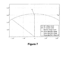
- Figure 7 illustrates a second exemplary set of operating points for the first voltage source converter operating at a positive real power and a positive quadrature power.
- the terms “reactor voltage vector” refers to the voltage vector of the phase reactance
- the term “shunt chainlink” refers to the DC side sub-converter 38
- the term “series chainlink” refers to the AC side sub-converter 39.
- Figure 8a shows the voltages and currents at a point of common coupling for the first voltage source converter 30 operating at 600 MW with -200M VAr corresponding to the vector diagram shown in Figure 7 .
- Figure 8b illustrates the formation of an AC phase voltage through operation of an AC side sub-converter 39 to generate a second compensation voltage. It can be seen that that there is a phase difference between the trapezoidal AC side voltage 63 and the AC phase voltage 67, and the second compensation voltage 71 is relatively larger than the first compensation voltage 69.
- each AC side sub-converter 39 to add and subtract voltage steps permits variation in the value of the phase reactance to reduce the required voltage range and optimise the associated losses of the AC side sub-converters 39.
- the plurality of AC phase voltages may become imbalanced.
- Such imbalance between the plurality of AC phase voltages can not only adversely affect the transfer of power between the AC and DC networks 50,58, but also disturb the regulation of the energy levels of the AC side sub-converters 39.
- each DC side sub-converter 38 may operate as a waveform synthesizer to control each DC side voltage so as to generate a plurality of imbalanced DC side voltages.
- each DC side sub-converter 38 in the first voltage source converter 30 permits each DC side sub-converter 38 to control the respective DC side voltage independently of the control of the other DC side voltages by the other DC side sub-converters 38.
- the magnitude of each DC side voltage can therefore be set to result in the generation of a plurality of imbalanced AC side voltages that is configured to compensate for the imbalance between the AC phase voltages.
- the operation of the DC side sub-converters 38 to enable presentation of a constant DC voltage to the DC network 58 is performed at the same time as the control of each DC side voltage so as to generate the plurality of imbalanced DC side voltages.
- the first voltage source converter 30 may be required to exchange reactive power with the AC network 50. Under such circumstances, the resulting discontinuity in each AC phase current means that the stray inductance on the AC side 42 of each phase element 36 of the first voltage source converter 30 requires an infinite AC phase voltage at the instant of the discontinuity, thus preventing the soft-switching of the plurality of switching elements 40 of the phase elements 36.
- the controller may operate each AC side sub-converter 39 as a waveform synthesizer to control each AC side voltage so as to drive the voltage across each of the plurality of switching elements 40 to a zero or substantially zero value during the switching of the plurality of switching elements 40 of the corresponding phase element 36, thus permitting the soft-switching of the plurality of switching elements 40 of the phase elements 36.
- the energy storage devices 56 of the AC side sub-converters 39 maintain the flow of the AC phase currents at the AC sides 42 of the phase elements 36.
- AC side sub-converters 39 may be rated specifically for the above additional functions, in addition to enabling the cancellation of the or each selected harmonic voltage component from the respective AC side voltages.
- a second voltage source converter 130 according to a second embodiment of the invention is shown in Figure 9 and is designated generally by the reference numeral 130.
- the second voltage source converter 130 is similar in structure and operation to the first voltage source converter 30, and like features share the same reference numerals.
- the second voltage source converter 130 differs from the first voltage source converter 30 in that, in the second voltage source converter 130, each limb further includes a respective tertiary transformer winding 70 that is magnetically coupled to the corresponding secondary transformer winding 44.
- the plurality of tertiary transformer windings 70 are electrically interconnected in a delta arrangement.
- each secondary transformer winding 44 having a low or zero impedance at zero-sequence harmonic frequencies, which permits the plurality of tertiary transformer windings 70 to act as a filter to zero-sequence harmonic components.
- This allows a corresponding reduction in the rating of each AC side sub-converter 39, since the AC side sub-converters 39 are no longer required to control the AC side voltages to cancel any zero sequence harmonic component synthesised by the DC side converters 38.
- each limb may include a respective reactor (not shown) connected in series with the corresponding secondary transformer winding 44.
- the provision of the series-connected reactors provides control over the currents in the respective secondary transformer windings 44, and thereby acts to limit the rise in harmonic current in the respective secondary transformer windings 44 when the plurality of tertiary transformer windings 70 acts as a filter to the zero-sequence harmonic components.
- controller 60 may be programmed to selectively operate each AC side sub-converter 39 as a waveform synthesizer to control the current in the corresponding secondary transformer winding 44 so as to limit or block the circulation of the zero-sequence harmonic components between the AC phases.
- the operation of the AC side sub-converters 39 in this manner provides control over the currents in the respective secondary transformer windings 44, and thereby acts to limit the rise in harmonic current in the respective secondary transformer windings 44 when the plurality of tertiary transformer windings 70 acts as a filter to the zero-sequence harmonic components.
- controller 60 may be programmed to selectively operate each AC side sub-converter 39 as a waveform synthesizer to control the voltage across the corresponding secondary transformer winding 44 to exchange power between the AC phases via the magnetically coupled secondary and tertiary transformer windings 44,70.
- the exchange of power via the magnetically coupled windings 44,70 provides a compact and reliable means of exchanging power between the AC phases.
- Exchanging power between the AC phases via the magnetically coupled windings 44,70 may include compensating for an imbalance between the AC phase voltages. Such compensation not only may be applied to the regulation of the energy levels of the AC side sub-converters 39 that have been adversely affected by the imbalance between the AC phase voltages, but also reduces or eliminates the need for the DC side sub-converters 38 to generate the plurality of imbalanced DC side voltages.
- the control of the voltage across the corresponding secondary transformer winding 44 to exchange power between the AC phases via the magnetically coupled windings 44,70 may include injection of a zero sequence harmonic voltage component into the voltage across the corresponding secondary transformer winding 44.
- a third voltage source converter 230 according to a third embodiment of the invention is shown in Figure 10 and is designated generally by the reference numeral 230.
- the third voltage source converter 230 is similar in structure and operation to the second voltage source converter 130, and like features share the same reference numerals.
- the third voltage source converter 230 differs from the second voltage source converter 130 in that, in the third voltage source converter 230, each limb includes a respective AC side reactor L AC connected in series with the corresponding secondary transformer winding 44 and the corresponding AC side sub-converter 39, instead of the respective tertiary transformer winding 70.
- Each AC side reactor L AC is in the form of a winding that is magnetically coupled to each of the other AC side reactors L AC .
- the configuration of the AC side reactors L AC in this manner provides a way of filtering one or more harmonic components by providing a high impedance to the or each harmonic component to be filtered. This also allows a corresponding reduction in the rating of each AC side sub-converter 39.
- the exchange of power between the AC phases may be carried out through the controller being programmed to selectively operate each AC side sub-converter 39 as a waveform synthesizer to control the voltage across the corresponding AC side reactor L AC to exchange power between the AC phases via the magnetically coupled AC side reactors L AC .
- a fourth voltage source converter 330 according to a fourth embodiment of the invention is shown in Figure 11 and is designated generally by the reference numeral 330.
- the fourth voltage source converter 330 is similar in structure and operation to the second voltage source converter 130, and like features share the same reference numerals.
- the fourth voltage source converter 330 differs from the second voltage source converter 130 in that, in the fourth voltage source converter 330, each limb includes a respective further winding 72 connected in series with the corresponding secondary transformer winding 44 and the corresponding AC side sub-converter 39, instead of the respective tertiary transformer winding 70.
- Each further winding 72 is magnetically coupled to a respective one of a plurality of additional windings 74, and the plurality of additional windings 74 are electrically connected in parallel.
- the configuration of the further and additional windings 72,74 in this manner provides another way of filtering one or more harmonic components by providing a high impedance to the or each harmonic component to be filtered. This also allows a corresponding reduction in the rating of each AC side sub-converter 39.
- the exchange of power between the AC phases may be carried out through the controller being programmed to selectively operate each AC side sub-converter 39 as a waveform synthesizer to control the voltage across the corresponding further winding 72 to exchange power between the AC phases via the magnetically coupled further and additional windings 72,74.
- the AC side 42 of each phase element 36 is connected to a respective phase of a three-phase AC network 50. It is envisaged that, in other embodiments, the number of limbs in the voltage source converter may vary with the number of phases of a multi-phase AC network, and the AC side of each phase element may be connected to a respective AC phase of the multi-phase phase AC network.
- the voltage source converter may include a single phase limb, whereby the AC side of the phase element is connected to an AC phase of a single-phase AC network.
Landscapes
- Engineering & Computer Science (AREA)
- Power Engineering (AREA)
- Rectifiers (AREA)
Priority Applications (1)
| Application Number | Priority Date | Filing Date | Title |
|---|---|---|---|
| EP15275074.1A EP3070826B1 (fr) | 2015-03-18 | 2015-03-18 | Convertisseur de source de tension |
Applications Claiming Priority (1)
| Application Number | Priority Date | Filing Date | Title |
|---|---|---|---|
| EP15275074.1A EP3070826B1 (fr) | 2015-03-18 | 2015-03-18 | Convertisseur de source de tension |
Publications (2)
| Publication Number | Publication Date |
|---|---|
| EP3070826A1 true EP3070826A1 (fr) | 2016-09-21 |
| EP3070826B1 EP3070826B1 (fr) | 2020-03-04 |
Family
ID=52697332
Family Applications (1)
| Application Number | Title | Priority Date | Filing Date |
|---|---|---|---|
| EP15275074.1A Active EP3070826B1 (fr) | 2015-03-18 | 2015-03-18 | Convertisseur de source de tension |
Country Status (1)
| Country | Link |
|---|---|
| EP (1) | EP3070826B1 (fr) |
Citations (2)
| Publication number | Priority date | Publication date | Assignee | Title |
|---|---|---|---|---|
| US20130128629A1 (en) * | 2010-04-15 | 2013-05-23 | Alstom Technology Ltd | Hybrid 2-level and multilevel hvdc converter |
| EP2755315A1 (fr) * | 2013-01-11 | 2014-07-16 | Alstom Technology Ltd | Convertisseur hybride et modulaire |
Family Cites Families (1)
| Publication number | Priority date | Publication date | Assignee | Title |
|---|---|---|---|---|
| EP2534742B8 (fr) * | 2010-02-09 | 2016-02-24 | General Electric Technology GmbH | Convertisseur pour transmission continu-continu à haute tension |
-
2015
- 2015-03-18 EP EP15275074.1A patent/EP3070826B1/fr active Active
Patent Citations (2)
| Publication number | Priority date | Publication date | Assignee | Title |
|---|---|---|---|---|
| US20130128629A1 (en) * | 2010-04-15 | 2013-05-23 | Alstom Technology Ltd | Hybrid 2-level and multilevel hvdc converter |
| EP2755315A1 (fr) * | 2013-01-11 | 2014-07-16 | Alstom Technology Ltd | Convertisseur hybride et modulaire |
Also Published As
| Publication number | Publication date |
|---|---|
| EP3070826B1 (fr) | 2020-03-04 |
Similar Documents
| Publication | Publication Date | Title |
|---|---|---|
| EP2863534B1 (fr) | Convertisseur de source de tension | |
| CA2793701C (fr) | Convertisseur ccht hybride | |
| US9831759B2 (en) | Voltage source converter | |
| EP3053242B1 (fr) | Convertisseur de source de tension | |
| CN110574278B (zh) | 电压源转换器 | |
| WO2015062975A1 (fr) | Convertisseur de source de tension | |
| EP2816718A1 (fr) | Convertisseur de puissance à plusieurs niveaux | |
| EP3352354B1 (fr) | Convertisseur de source de tension | |
| US10985671B2 (en) | Alternate arm converter | |
| EP3070826B1 (fr) | Convertisseur de source de tension | |
| EP3582379B1 (fr) | Convertisseur de source de tension | |
| CA2993752A1 (fr) | Convertisseur de source de tension | |
| EP3512088B1 (fr) | Convertisseur de source de tension | |
| Chakrabarti et al. | A Fault Tolerant Control Scheme of Grid Connected VSI for Balanced Power Injection |
Legal Events
| Date | Code | Title | Description |
|---|---|---|---|
| PUAI | Public reference made under article 153(3) epc to a published international application that has entered the european phase |
Free format text: ORIGINAL CODE: 0009012 |
|
| AK | Designated contracting states |
Kind code of ref document: A1 Designated state(s): AL AT BE BG CH CY CZ DE DK EE ES FI FR GB GR HR HU IE IS IT LI LT LU LV MC MK MT NL NO PL PT RO RS SE SI SK SM TR |
|
| AX | Request for extension of the european patent |
Extension state: BA ME |
|
| RAP1 | Party data changed (applicant data changed or rights of an application transferred) |
Owner name: GENERAL ELECTRIC TECHNOLOGY GMBH |
|
| STAA | Information on the status of an ep patent application or granted ep patent |
Free format text: STATUS: REQUEST FOR EXAMINATION WAS MADE |
|
| 17P | Request for examination filed |
Effective date: 20170321 |
|
| RBV | Designated contracting states (corrected) |
Designated state(s): AL AT BE BG CH CY CZ DE DK EE ES FI FR GB GR HR HU IE IS IT LI LT LU LV MC MK MT NL NO PL PT RO RS SE SI SK SM TR |
|
| GRAJ | Information related to disapproval of communication of intention to grant by the applicant or resumption of examination proceedings by the epo deleted |
Free format text: ORIGINAL CODE: EPIDOSDIGR1 |
|
| GRAP | Despatch of communication of intention to grant a patent |
Free format text: ORIGINAL CODE: EPIDOSNIGR1 |
|
| GRAP | Despatch of communication of intention to grant a patent |
Free format text: ORIGINAL CODE: EPIDOSNIGR1 |
|
| STAA | Information on the status of an ep patent application or granted ep patent |
Free format text: STATUS: GRANT OF PATENT IS INTENDED |
|
| INTG | Intention to grant announced |
Effective date: 20190904 |
|
| GRAS | Grant fee paid |
Free format text: ORIGINAL CODE: EPIDOSNIGR3 |
|
| GRAJ | Information related to disapproval of communication of intention to grant by the applicant or resumption of examination proceedings by the epo deleted |
Free format text: ORIGINAL CODE: EPIDOSDIGR1 |
|
| GRAL | Information related to payment of fee for publishing/printing deleted |
Free format text: ORIGINAL CODE: EPIDOSDIGR3 |
|
| STAA | Information on the status of an ep patent application or granted ep patent |
Free format text: STATUS: REQUEST FOR EXAMINATION WAS MADE |
|
| GRAR | Information related to intention to grant a patent recorded |
Free format text: ORIGINAL CODE: EPIDOSNIGR71 |
|
| STAA | Information on the status of an ep patent application or granted ep patent |
Free format text: STATUS: GRANT OF PATENT IS INTENDED |
|
| GRAA | (expected) grant |
Free format text: ORIGINAL CODE: 0009210 |
|
| STAA | Information on the status of an ep patent application or granted ep patent |
Free format text: STATUS: THE PATENT HAS BEEN GRANTED |
|
| INTC | Intention to grant announced (deleted) | ||
| AK | Designated contracting states |
Kind code of ref document: B1 Designated state(s): AL AT BE BG CH CY CZ DE DK EE ES FI FR GB GR HR HU IE IS IT LI LT LU LV MC MK MT NL NO PL PT RO RS SE SI SK SM TR |
|
| INTG | Intention to grant announced |
Effective date: 20200124 |
|
| REG | Reference to a national code |
Ref country code: GB Ref legal event code: FG4D |
|
| REG | Reference to a national code |
Ref country code: CH Ref legal event code: EP |
|
| REG | Reference to a national code |
Ref country code: AT Ref legal event code: REF Ref document number: 1241522 Country of ref document: AT Kind code of ref document: T Effective date: 20200315 |
|
| REG | Reference to a national code |
Ref country code: DE Ref legal event code: R096 Ref document number: 602015048082 Country of ref document: DE |
|
| REG | Reference to a national code |
Ref country code: IE Ref legal event code: FG4D |
|
| REG | Reference to a national code |
Ref country code: SE Ref legal event code: TRGR |
|
| PG25 | Lapsed in a contracting state [announced via postgrant information from national office to epo] |
Ref country code: NO Free format text: LAPSE BECAUSE OF FAILURE TO SUBMIT A TRANSLATION OF THE DESCRIPTION OR TO PAY THE FEE WITHIN THE PRESCRIBED TIME-LIMIT Effective date: 20200604 Ref country code: RS Free format text: LAPSE BECAUSE OF FAILURE TO SUBMIT A TRANSLATION OF THE DESCRIPTION OR TO PAY THE FEE WITHIN THE PRESCRIBED TIME-LIMIT Effective date: 20200304 Ref country code: FI Free format text: LAPSE BECAUSE OF FAILURE TO SUBMIT A TRANSLATION OF THE DESCRIPTION OR TO PAY THE FEE WITHIN THE PRESCRIBED TIME-LIMIT Effective date: 20200304 |
|
| REG | Reference to a national code |
Ref country code: NL Ref legal event code: MP Effective date: 20200304 |
|
| PG25 | Lapsed in a contracting state [announced via postgrant information from national office to epo] |
Ref country code: GR Free format text: LAPSE BECAUSE OF FAILURE TO SUBMIT A TRANSLATION OF THE DESCRIPTION OR TO PAY THE FEE WITHIN THE PRESCRIBED TIME-LIMIT Effective date: 20200605 Ref country code: HR Free format text: LAPSE BECAUSE OF FAILURE TO SUBMIT A TRANSLATION OF THE DESCRIPTION OR TO PAY THE FEE WITHIN THE PRESCRIBED TIME-LIMIT Effective date: 20200304 Ref country code: LV Free format text: LAPSE BECAUSE OF FAILURE TO SUBMIT A TRANSLATION OF THE DESCRIPTION OR TO PAY THE FEE WITHIN THE PRESCRIBED TIME-LIMIT Effective date: 20200304 Ref country code: BG Free format text: LAPSE BECAUSE OF FAILURE TO SUBMIT A TRANSLATION OF THE DESCRIPTION OR TO PAY THE FEE WITHIN THE PRESCRIBED TIME-LIMIT Effective date: 20200604 |
|
| REG | Reference to a national code |
Ref country code: LT Ref legal event code: MG4D |
|
| PG25 | Lapsed in a contracting state [announced via postgrant information from national office to epo] |
Ref country code: NL Free format text: LAPSE BECAUSE OF FAILURE TO SUBMIT A TRANSLATION OF THE DESCRIPTION OR TO PAY THE FEE WITHIN THE PRESCRIBED TIME-LIMIT Effective date: 20200304 |
|
| PG25 | Lapsed in a contracting state [announced via postgrant information from national office to epo] |
Ref country code: ES Free format text: LAPSE BECAUSE OF FAILURE TO SUBMIT A TRANSLATION OF THE DESCRIPTION OR TO PAY THE FEE WITHIN THE PRESCRIBED TIME-LIMIT Effective date: 20200304 Ref country code: PT Free format text: LAPSE BECAUSE OF FAILURE TO SUBMIT A TRANSLATION OF THE DESCRIPTION OR TO PAY THE FEE WITHIN THE PRESCRIBED TIME-LIMIT Effective date: 20200729 Ref country code: EE Free format text: LAPSE BECAUSE OF FAILURE TO SUBMIT A TRANSLATION OF THE DESCRIPTION OR TO PAY THE FEE WITHIN THE PRESCRIBED TIME-LIMIT Effective date: 20200304 Ref country code: LT Free format text: LAPSE BECAUSE OF FAILURE TO SUBMIT A TRANSLATION OF THE DESCRIPTION OR TO PAY THE FEE WITHIN THE PRESCRIBED TIME-LIMIT Effective date: 20200304 Ref country code: CZ Free format text: LAPSE BECAUSE OF FAILURE TO SUBMIT A TRANSLATION OF THE DESCRIPTION OR TO PAY THE FEE WITHIN THE PRESCRIBED TIME-LIMIT Effective date: 20200304 Ref country code: RO Free format text: LAPSE BECAUSE OF FAILURE TO SUBMIT A TRANSLATION OF THE DESCRIPTION OR TO PAY THE FEE WITHIN THE PRESCRIBED TIME-LIMIT Effective date: 20200304 Ref country code: SK Free format text: LAPSE BECAUSE OF FAILURE TO SUBMIT A TRANSLATION OF THE DESCRIPTION OR TO PAY THE FEE WITHIN THE PRESCRIBED TIME-LIMIT Effective date: 20200304 Ref country code: SM Free format text: LAPSE BECAUSE OF FAILURE TO SUBMIT A TRANSLATION OF THE DESCRIPTION OR TO PAY THE FEE WITHIN THE PRESCRIBED TIME-LIMIT Effective date: 20200304 Ref country code: IS Free format text: LAPSE BECAUSE OF FAILURE TO SUBMIT A TRANSLATION OF THE DESCRIPTION OR TO PAY THE FEE WITHIN THE PRESCRIBED TIME-LIMIT Effective date: 20200704 |
|
| REG | Reference to a national code |
Ref country code: CH Ref legal event code: PL |
|
| REG | Reference to a national code |
Ref country code: AT Ref legal event code: MK05 Ref document number: 1241522 Country of ref document: AT Kind code of ref document: T Effective date: 20200304 |
|
| REG | Reference to a national code |
Ref country code: DE Ref legal event code: R097 Ref document number: 602015048082 Country of ref document: DE |
|
| REG | Reference to a national code |
Ref country code: BE Ref legal event code: MM Effective date: 20200331 |
|
| PG25 | Lapsed in a contracting state [announced via postgrant information from national office to epo] |
Ref country code: LU Free format text: LAPSE BECAUSE OF NON-PAYMENT OF DUE FEES Effective date: 20200318 Ref country code: MC Free format text: LAPSE BECAUSE OF FAILURE TO SUBMIT A TRANSLATION OF THE DESCRIPTION OR TO PAY THE FEE WITHIN THE PRESCRIBED TIME-LIMIT Effective date: 20200304 |
|
| PLBE | No opposition filed within time limit |
Free format text: ORIGINAL CODE: 0009261 |
|
| STAA | Information on the status of an ep patent application or granted ep patent |
Free format text: STATUS: NO OPPOSITION FILED WITHIN TIME LIMIT |
|
| PG25 | Lapsed in a contracting state [announced via postgrant information from national office to epo] |
Ref country code: IT Free format text: LAPSE BECAUSE OF FAILURE TO SUBMIT A TRANSLATION OF THE DESCRIPTION OR TO PAY THE FEE WITHIN THE PRESCRIBED TIME-LIMIT Effective date: 20200304 Ref country code: AT Free format text: LAPSE BECAUSE OF FAILURE TO SUBMIT A TRANSLATION OF THE DESCRIPTION OR TO PAY THE FEE WITHIN THE PRESCRIBED TIME-LIMIT Effective date: 20200304 Ref country code: IE Free format text: LAPSE BECAUSE OF NON-PAYMENT OF DUE FEES Effective date: 20200318 Ref country code: CH Free format text: LAPSE BECAUSE OF NON-PAYMENT OF DUE FEES Effective date: 20200331 Ref country code: DK Free format text: LAPSE BECAUSE OF FAILURE TO SUBMIT A TRANSLATION OF THE DESCRIPTION OR TO PAY THE FEE WITHIN THE PRESCRIBED TIME-LIMIT Effective date: 20200304 Ref country code: LI Free format text: LAPSE BECAUSE OF NON-PAYMENT OF DUE FEES Effective date: 20200331 |
|
| 26N | No opposition filed |
Effective date: 20201207 |
|
| PG25 | Lapsed in a contracting state [announced via postgrant information from national office to epo] |
Ref country code: BE Free format text: LAPSE BECAUSE OF NON-PAYMENT OF DUE FEES Effective date: 20200331 Ref country code: SI Free format text: LAPSE BECAUSE OF FAILURE TO SUBMIT A TRANSLATION OF THE DESCRIPTION OR TO PAY THE FEE WITHIN THE PRESCRIBED TIME-LIMIT Effective date: 20200304 Ref country code: PL Free format text: LAPSE BECAUSE OF FAILURE TO SUBMIT A TRANSLATION OF THE DESCRIPTION OR TO PAY THE FEE WITHIN THE PRESCRIBED TIME-LIMIT Effective date: 20200304 |
|
| PG25 | Lapsed in a contracting state [announced via postgrant information from national office to epo] |
Ref country code: FR Free format text: LAPSE BECAUSE OF NON-PAYMENT OF DUE FEES Effective date: 20200504 |
|
| PG25 | Lapsed in a contracting state [announced via postgrant information from national office to epo] |
Ref country code: TR Free format text: LAPSE BECAUSE OF FAILURE TO SUBMIT A TRANSLATION OF THE DESCRIPTION OR TO PAY THE FEE WITHIN THE PRESCRIBED TIME-LIMIT Effective date: 20200304 Ref country code: MT Free format text: LAPSE BECAUSE OF FAILURE TO SUBMIT A TRANSLATION OF THE DESCRIPTION OR TO PAY THE FEE WITHIN THE PRESCRIBED TIME-LIMIT Effective date: 20200304 Ref country code: CY Free format text: LAPSE BECAUSE OF FAILURE TO SUBMIT A TRANSLATION OF THE DESCRIPTION OR TO PAY THE FEE WITHIN THE PRESCRIBED TIME-LIMIT Effective date: 20200304 |
|
| PG25 | Lapsed in a contracting state [announced via postgrant information from national office to epo] |
Ref country code: MK Free format text: LAPSE BECAUSE OF FAILURE TO SUBMIT A TRANSLATION OF THE DESCRIPTION OR TO PAY THE FEE WITHIN THE PRESCRIBED TIME-LIMIT Effective date: 20200304 Ref country code: AL Free format text: LAPSE BECAUSE OF FAILURE TO SUBMIT A TRANSLATION OF THE DESCRIPTION OR TO PAY THE FEE WITHIN THE PRESCRIBED TIME-LIMIT Effective date: 20200304 |
|
| PGFP | Annual fee paid to national office [announced via postgrant information from national office to epo] |
Ref country code: SE Payment date: 20230222 Year of fee payment: 9 Ref country code: GB Payment date: 20230221 Year of fee payment: 9 Ref country code: DE Payment date: 20230221 Year of fee payment: 9 |
|
| P01 | Opt-out of the competence of the unified patent court (upc) registered |
Effective date: 20230522 |