EP3070757A1 - Organic electroluminescent device and method for manufacture thereof - Google Patents
Organic electroluminescent device and method for manufacture thereof Download PDFInfo
- Publication number
- EP3070757A1 EP3070757A1 EP14872476.8A EP14872476A EP3070757A1 EP 3070757 A1 EP3070757 A1 EP 3070757A1 EP 14872476 A EP14872476 A EP 14872476A EP 3070757 A1 EP3070757 A1 EP 3070757A1
- Authority
- EP
- European Patent Office
- Prior art keywords
- phenyl
- substituted
- alkyl
- organic electroluminescent
- ethyoxyl
- Prior art date
- Legal status (The legal status is an assumption and is not a legal conclusion. Google has not performed a legal analysis and makes no representation as to the accuracy of the status listed.)
- Granted
Links
- 0 CC*(C)C=C[C@@](C)N(CCCC(N)=CCC)*1(*=*=CC1)OC Chemical compound CC*(C)C=C[C@@](C)N(CCCC(N)=CCC)*1(*=*=CC1)OC 0.000 description 2
- AJQBILKBVIQSPU-UHFFFAOYSA-N CC1C=Cc2c(-c3ccc[s]3)c3n[s]nc3c(-c(cc3)ccc3N(c3ccccc3)c3ccccc3)c2C1 Chemical compound CC1C=Cc2c(-c3ccc[s]3)c3n[s]nc3c(-c(cc3)ccc3N(c3ccccc3)c3ccccc3)c2C1 AJQBILKBVIQSPU-UHFFFAOYSA-N 0.000 description 1
- ISVJEOQEDRVYAL-UHFFFAOYSA-N CC1N=C2c3ccccc3-c3ccccc3C2N1C Chemical compound CC1N=C2c3ccccc3-c3ccccc3C2N1C ISVJEOQEDRVYAL-UHFFFAOYSA-N 0.000 description 1
- ACWPRLJPSFFMRN-SOWVJEBXSA-N CCC[IH](CCC=C1)=C1N(CC(CC1)[IH]c(c([Tl])c2/C=C\C)c1[n]2-c1nc(/C=C/C=C\CC)nc(Nc(c(/C(/C)=C/CCC=C)c2)ccc2-[n]2c(C=CCC=C3)c3c3ccccc23)n1)C(C)/C=C\C Chemical compound CCC[IH](CCC=C1)=C1N(CC(CC1)[IH]c(c([Tl])c2/C=C\C)c1[n]2-c1nc(/C=C/C=C\CC)nc(Nc(c(/C(/C)=C/CCC=C)c2)ccc2-[n]2c(C=CCC=C3)c3c3ccccc23)n1)C(C)/C=C\C ACWPRLJPSFFMRN-SOWVJEBXSA-N 0.000 description 1
- CCECUAHRFQGOMQ-UHFFFAOYSA-N Cc1c(cccc2)c2c(C)c2n[s]nc12 Chemical compound Cc1c(cccc2)c2c(C)c2n[s]nc12 CCECUAHRFQGOMQ-UHFFFAOYSA-N 0.000 description 1
- HGMZVWRYEANWTD-UHFFFAOYSA-N Cc1ccc(C)c2n[s]nc12 Chemical compound Cc1ccc(C)c2n[s]nc12 HGMZVWRYEANWTD-UHFFFAOYSA-N 0.000 description 1
- STTGYIUESPWXOW-UHFFFAOYSA-N Cc1nc(c2nc(C)cc(-c3ccccc3)c2cc2)c2c(-c2ccccc2)c1 Chemical compound Cc1nc(c2nc(C)cc(-c3ccccc3)c2cc2)c2c(-c2ccccc2)c1 STTGYIUESPWXOW-UHFFFAOYSA-N 0.000 description 1
- YVDWFZIVIIKYBQ-UHFFFAOYSA-N Cc1nnc(C)[o]1 Chemical compound Cc1nnc(C)[o]1 YVDWFZIVIIKYBQ-UHFFFAOYSA-N 0.000 description 1
- YFOHWVZJAFEMKE-UHFFFAOYSA-N O=[SH-](c(cc1)ccc1-[n]1c(ccc(-c2ccccc2)c2)c2c2ccccc12)c(cc1)ccc1-[n](c(cccc1)c1c1c2)c1ccc2-c1ccccc1 Chemical compound O=[SH-](c(cc1)ccc1-[n]1c(ccc(-c2ccccc2)c2)c2c2ccccc12)c(cc1)ccc1-[n](c(cccc1)c1c1c2)c1ccc2-c1ccccc1 YFOHWVZJAFEMKE-UHFFFAOYSA-N 0.000 description 1
- TWLHIDGFFOHAGH-UHFFFAOYSA-N O[S-](c(cc1)ccc1-[n](c(cccc1)c1c1c2)c1ccc2-[n]1c2ccccc2c2c1cccc2)(c(cc1)ccc1-[n]1c(ccc(-[n]2c3ccccc3c3ccccc23)c2)c2c2ccccc12)=O Chemical compound O[S-](c(cc1)ccc1-[n](c(cccc1)c1c1c2)c1ccc2-[n]1c2ccccc2c2c1cccc2)(c(cc1)ccc1-[n]1c(ccc(-[n]2c3ccccc3c3ccccc23)c2)c2c2ccccc12)=O TWLHIDGFFOHAGH-UHFFFAOYSA-N 0.000 description 1
- FXOPNNZOEPMMQV-UHFFFAOYSA-N c(cc1)ccc1-c(c1n[s]nc11)c(cccc2)c2c1-c(cc1)ccc1N(c1ccccc1)c1ccccc1 Chemical compound c(cc1)ccc1-c(c1n[s]nc11)c(cccc2)c2c1-c(cc1)ccc1N(c1ccccc1)c1ccccc1 FXOPNNZOEPMMQV-UHFFFAOYSA-N 0.000 description 1
- DHDHJYNTEFLIHY-UHFFFAOYSA-N c(cc1)ccc1-c1c(ccc(c2ncc3)c3-c3ccccc3)c2ncc1 Chemical compound c(cc1)ccc1-c1c(ccc(c2ncc3)c3-c3ccccc3)c2ncc1 DHDHJYNTEFLIHY-UHFFFAOYSA-N 0.000 description 1
- RYBHBXOLGCIDJA-UHFFFAOYSA-N c(cc1)ccc1-c1nc(-c(cc2)ccc2-[n]2c3ccccc3c3c2cccc3)nc(-c(cc2)ccc2-[n]2c3ccccc3c3ccccc23)n1 Chemical compound c(cc1)ccc1-c1nc(-c(cc2)ccc2-[n]2c3ccccc3c3c2cccc3)nc(-c(cc2)ccc2-[n]2c3ccccc3c3ccccc23)n1 RYBHBXOLGCIDJA-UHFFFAOYSA-N 0.000 description 1
- ZABORCXHTNWZRV-UHFFFAOYSA-N c(cc1)ccc1-c1nc(-c(cc2)ccc2N2c(cccc3)c3Oc3ccccc23)nc(-c2ccccc2)n1 Chemical compound c(cc1)ccc1-c1nc(-c(cc2)ccc2N2c(cccc3)c3Oc3ccccc23)nc(-c2ccccc2)n1 ZABORCXHTNWZRV-UHFFFAOYSA-N 0.000 description 1
- SWUBEMMFTUPINB-UHFFFAOYSA-N c(cc1)ccc1-c1nc(-c2cc(-[n]3c4ccccc4c4c3cccc4)cc(-[n]3c4ccccc4c4c3cccc4)c2)nc(-c2ccccc2)n1 Chemical compound c(cc1)ccc1-c1nc(-c2cc(-[n]3c4ccccc4c4c3cccc4)cc(-[n]3c4ccccc4c4c3cccc4)c2)nc(-c2ccccc2)n1 SWUBEMMFTUPINB-UHFFFAOYSA-N 0.000 description 1
- XSKXKOZLUCZSLC-UHFFFAOYSA-N c(cc1)ccc1-c1nc(-c2cccc(N3c(cccc4)c4Oc4c3cccc4)c2)nc(-c2cccc(N3c(cccc4)c4Oc4c3cccc4)c2)n1 Chemical compound c(cc1)ccc1-c1nc(-c2cccc(N3c(cccc4)c4Oc4c3cccc4)c2)nc(-c2cccc(N3c(cccc4)c4Oc4c3cccc4)c2)n1 XSKXKOZLUCZSLC-UHFFFAOYSA-N 0.000 description 1
- ASHFOTPVKVKBHQ-UHFFFAOYSA-N c(cc1)ccc1-c1nnc(-c(cc2)ccc2N2c(cccc3)c3Oc3c2cccc3)[n]1-c1ccccc1 Chemical compound c(cc1)ccc1-c1nnc(-c(cc2)ccc2N2c(cccc3)c3Oc3c2cccc3)[n]1-c1ccccc1 ASHFOTPVKVKBHQ-UHFFFAOYSA-N 0.000 description 1
- BKWVNXPZFIACTJ-UHFFFAOYSA-N c(cc1)ccc1-c1nnc(-c(cc2)ccc2N2c(cccc3)c3Oc3c2cccc3)[o]1 Chemical compound c(cc1)ccc1-c1nnc(-c(cc2)ccc2N2c(cccc3)c3Oc3c2cccc3)[o]1 BKWVNXPZFIACTJ-UHFFFAOYSA-N 0.000 description 1
Images


Classifications
-
- C—CHEMISTRY; METALLURGY
- C09—DYES; PAINTS; POLISHES; NATURAL RESINS; ADHESIVES; COMPOSITIONS NOT OTHERWISE PROVIDED FOR; APPLICATIONS OF MATERIALS NOT OTHERWISE PROVIDED FOR
- C09K—MATERIALS FOR MISCELLANEOUS APPLICATIONS, NOT PROVIDED FOR ELSEWHERE
- C09K11/00—Luminescent materials, e.g. electroluminescent or chemiluminescent
- C09K11/02—Use of particular materials as binders, particle coatings or suspension media therefor
- C09K11/025—Use of particular materials as binders, particle coatings or suspension media therefor non-luminescent particle coatings or suspension media
-
- H—ELECTRICITY
- H10—SEMICONDUCTOR DEVICES; ELECTRIC SOLID-STATE DEVICES NOT OTHERWISE PROVIDED FOR
- H10K—ORGANIC ELECTRIC SOLID-STATE DEVICES
- H10K50/00—Organic light-emitting devices
- H10K50/10—OLEDs or polymer light-emitting diodes [PLED]
- H10K50/11—OLEDs or polymer light-emitting diodes [PLED] characterised by the electroluminescent [EL] layers
-
- C—CHEMISTRY; METALLURGY
- C09—DYES; PAINTS; POLISHES; NATURAL RESINS; ADHESIVES; COMPOSITIONS NOT OTHERWISE PROVIDED FOR; APPLICATIONS OF MATERIALS NOT OTHERWISE PROVIDED FOR
- C09K—MATERIALS FOR MISCELLANEOUS APPLICATIONS, NOT PROVIDED FOR ELSEWHERE
- C09K11/00—Luminescent materials, e.g. electroluminescent or chemiluminescent
- C09K11/06—Luminescent materials, e.g. electroluminescent or chemiluminescent containing organic luminescent materials
-
- H—ELECTRICITY
- H10—SEMICONDUCTOR DEVICES; ELECTRIC SOLID-STATE DEVICES NOT OTHERWISE PROVIDED FOR
- H10K—ORGANIC ELECTRIC SOLID-STATE DEVICES
- H10K85/00—Organic materials used in the body or electrodes of devices covered by this subclass
- H10K85/60—Organic compounds having low molecular weight
- H10K85/611—Charge transfer complexes
-
- H—ELECTRICITY
- H10—SEMICONDUCTOR DEVICES; ELECTRIC SOLID-STATE DEVICES NOT OTHERWISE PROVIDED FOR
- H10K—ORGANIC ELECTRIC SOLID-STATE DEVICES
- H10K85/00—Organic materials used in the body or electrodes of devices covered by this subclass
- H10K85/60—Organic compounds having low molecular weight
- H10K85/615—Polycyclic condensed aromatic hydrocarbons, e.g. anthracene
- H10K85/622—Polycyclic condensed aromatic hydrocarbons, e.g. anthracene containing four rings, e.g. pyrene
-
- H—ELECTRICITY
- H10—SEMICONDUCTOR DEVICES; ELECTRIC SOLID-STATE DEVICES NOT OTHERWISE PROVIDED FOR
- H10K—ORGANIC ELECTRIC SOLID-STATE DEVICES
- H10K85/00—Organic materials used in the body or electrodes of devices covered by this subclass
- H10K85/60—Organic compounds having low molecular weight
- H10K85/615—Polycyclic condensed aromatic hydrocarbons, e.g. anthracene
- H10K85/624—Polycyclic condensed aromatic hydrocarbons, e.g. anthracene containing six or more rings
-
- H—ELECTRICITY
- H10—SEMICONDUCTOR DEVICES; ELECTRIC SOLID-STATE DEVICES NOT OTHERWISE PROVIDED FOR
- H10K—ORGANIC ELECTRIC SOLID-STATE DEVICES
- H10K85/00—Organic materials used in the body or electrodes of devices covered by this subclass
- H10K85/60—Organic compounds having low molecular weight
- H10K85/631—Amine compounds having at least two aryl rest on at least one amine-nitrogen atom, e.g. triphenylamine
- H10K85/633—Amine compounds having at least two aryl rest on at least one amine-nitrogen atom, e.g. triphenylamine comprising polycyclic condensed aromatic hydrocarbons as substituents on the nitrogen atom
-
- H—ELECTRICITY
- H10—SEMICONDUCTOR DEVICES; ELECTRIC SOLID-STATE DEVICES NOT OTHERWISE PROVIDED FOR
- H10K—ORGANIC ELECTRIC SOLID-STATE DEVICES
- H10K85/00—Organic materials used in the body or electrodes of devices covered by this subclass
- H10K85/60—Organic compounds having low molecular weight
- H10K85/631—Amine compounds having at least two aryl rest on at least one amine-nitrogen atom, e.g. triphenylamine
- H10K85/636—Amine compounds having at least two aryl rest on at least one amine-nitrogen atom, e.g. triphenylamine comprising heteroaromatic hydrocarbons as substituents on the nitrogen atom
-
- H—ELECTRICITY
- H10—SEMICONDUCTOR DEVICES; ELECTRIC SOLID-STATE DEVICES NOT OTHERWISE PROVIDED FOR
- H10K—ORGANIC ELECTRIC SOLID-STATE DEVICES
- H10K85/00—Organic materials used in the body or electrodes of devices covered by this subclass
- H10K85/60—Organic compounds having low molecular weight
- H10K85/649—Aromatic compounds comprising a hetero atom
- H10K85/653—Aromatic compounds comprising a hetero atom comprising only oxygen as heteroatom
-
- H—ELECTRICITY
- H10—SEMICONDUCTOR DEVICES; ELECTRIC SOLID-STATE DEVICES NOT OTHERWISE PROVIDED FOR
- H10K—ORGANIC ELECTRIC SOLID-STATE DEVICES
- H10K85/00—Organic materials used in the body or electrodes of devices covered by this subclass
- H10K85/60—Organic compounds having low molecular weight
- H10K85/649—Aromatic compounds comprising a hetero atom
- H10K85/654—Aromatic compounds comprising a hetero atom comprising only nitrogen as heteroatom
-
- H—ELECTRICITY
- H10—SEMICONDUCTOR DEVICES; ELECTRIC SOLID-STATE DEVICES NOT OTHERWISE PROVIDED FOR
- H10K—ORGANIC ELECTRIC SOLID-STATE DEVICES
- H10K85/00—Organic materials used in the body or electrodes of devices covered by this subclass
- H10K85/60—Organic compounds having low molecular weight
- H10K85/649—Aromatic compounds comprising a hetero atom
- H10K85/656—Aromatic compounds comprising a hetero atom comprising two or more different heteroatoms per ring
-
- H—ELECTRICITY
- H10—SEMICONDUCTOR DEVICES; ELECTRIC SOLID-STATE DEVICES NOT OTHERWISE PROVIDED FOR
- H10K—ORGANIC ELECTRIC SOLID-STATE DEVICES
- H10K85/00—Organic materials used in the body or electrodes of devices covered by this subclass
- H10K85/60—Organic compounds having low molecular weight
- H10K85/649—Aromatic compounds comprising a hetero atom
- H10K85/656—Aromatic compounds comprising a hetero atom comprising two or more different heteroatoms per ring
- H10K85/6565—Oxadiazole compounds
-
- H—ELECTRICITY
- H10—SEMICONDUCTOR DEVICES; ELECTRIC SOLID-STATE DEVICES NOT OTHERWISE PROVIDED FOR
- H10K—ORGANIC ELECTRIC SOLID-STATE DEVICES
- H10K85/00—Organic materials used in the body or electrodes of devices covered by this subclass
- H10K85/60—Organic compounds having low molecular weight
- H10K85/649—Aromatic compounds comprising a hetero atom
- H10K85/657—Polycyclic condensed heteroaromatic hydrocarbons
-
- H—ELECTRICITY
- H10—SEMICONDUCTOR DEVICES; ELECTRIC SOLID-STATE DEVICES NOT OTHERWISE PROVIDED FOR
- H10K—ORGANIC ELECTRIC SOLID-STATE DEVICES
- H10K85/00—Organic materials used in the body or electrodes of devices covered by this subclass
- H10K85/60—Organic compounds having low molecular weight
- H10K85/649—Aromatic compounds comprising a hetero atom
- H10K85/657—Polycyclic condensed heteroaromatic hydrocarbons
- H10K85/6572—Polycyclic condensed heteroaromatic hydrocarbons comprising only nitrogen in the heteroaromatic polycondensed ring system, e.g. phenanthroline or carbazole
-
- C—CHEMISTRY; METALLURGY
- C09—DYES; PAINTS; POLISHES; NATURAL RESINS; ADHESIVES; COMPOSITIONS NOT OTHERWISE PROVIDED FOR; APPLICATIONS OF MATERIALS NOT OTHERWISE PROVIDED FOR
- C09K—MATERIALS FOR MISCELLANEOUS APPLICATIONS, NOT PROVIDED FOR ELSEWHERE
- C09K2211/00—Chemical nature of organic luminescent or tenebrescent compounds
- C09K2211/10—Non-macromolecular compounds
- C09K2211/1003—Carbocyclic compounds
- C09K2211/1007—Non-condensed systems
-
- C—CHEMISTRY; METALLURGY
- C09—DYES; PAINTS; POLISHES; NATURAL RESINS; ADHESIVES; COMPOSITIONS NOT OTHERWISE PROVIDED FOR; APPLICATIONS OF MATERIALS NOT OTHERWISE PROVIDED FOR
- C09K—MATERIALS FOR MISCELLANEOUS APPLICATIONS, NOT PROVIDED FOR ELSEWHERE
- C09K2211/00—Chemical nature of organic luminescent or tenebrescent compounds
- C09K2211/10—Non-macromolecular compounds
- C09K2211/1003—Carbocyclic compounds
- C09K2211/1011—Condensed systems
-
- C—CHEMISTRY; METALLURGY
- C09—DYES; PAINTS; POLISHES; NATURAL RESINS; ADHESIVES; COMPOSITIONS NOT OTHERWISE PROVIDED FOR; APPLICATIONS OF MATERIALS NOT OTHERWISE PROVIDED FOR
- C09K—MATERIALS FOR MISCELLANEOUS APPLICATIONS, NOT PROVIDED FOR ELSEWHERE
- C09K2211/00—Chemical nature of organic luminescent or tenebrescent compounds
- C09K2211/10—Non-macromolecular compounds
- C09K2211/1018—Heterocyclic compounds
- C09K2211/1025—Heterocyclic compounds characterised by ligands
- C09K2211/1029—Heterocyclic compounds characterised by ligands containing one nitrogen atom as the heteroatom
-
- C—CHEMISTRY; METALLURGY
- C09—DYES; PAINTS; POLISHES; NATURAL RESINS; ADHESIVES; COMPOSITIONS NOT OTHERWISE PROVIDED FOR; APPLICATIONS OF MATERIALS NOT OTHERWISE PROVIDED FOR
- C09K—MATERIALS FOR MISCELLANEOUS APPLICATIONS, NOT PROVIDED FOR ELSEWHERE
- C09K2211/00—Chemical nature of organic luminescent or tenebrescent compounds
- C09K2211/10—Non-macromolecular compounds
- C09K2211/1018—Heterocyclic compounds
- C09K2211/1025—Heterocyclic compounds characterised by ligands
- C09K2211/1088—Heterocyclic compounds characterised by ligands containing oxygen as the only heteroatom
-
- H—ELECTRICITY
- H10—SEMICONDUCTOR DEVICES; ELECTRIC SOLID-STATE DEVICES NOT OTHERWISE PROVIDED FOR
- H10K—ORGANIC ELECTRIC SOLID-STATE DEVICES
- H10K2101/00—Properties of the organic materials covered by group H10K85/00
-
- H—ELECTRICITY
- H10—SEMICONDUCTOR DEVICES; ELECTRIC SOLID-STATE DEVICES NOT OTHERWISE PROVIDED FOR
- H10K—ORGANIC ELECTRIC SOLID-STATE DEVICES
- H10K2101/00—Properties of the organic materials covered by group H10K85/00
- H10K2101/10—Triplet emission
-
- H—ELECTRICITY
- H10—SEMICONDUCTOR DEVICES; ELECTRIC SOLID-STATE DEVICES NOT OTHERWISE PROVIDED FOR
- H10K—ORGANIC ELECTRIC SOLID-STATE DEVICES
- H10K2101/00—Properties of the organic materials covered by group H10K85/00
- H10K2101/20—Delayed fluorescence emission
-
- H—ELECTRICITY
- H10—SEMICONDUCTOR DEVICES; ELECTRIC SOLID-STATE DEVICES NOT OTHERWISE PROVIDED FOR
- H10K—ORGANIC ELECTRIC SOLID-STATE DEVICES
- H10K2101/00—Properties of the organic materials covered by group H10K85/00
- H10K2101/40—Interrelation of parameters between multiple constituent active layers or sublayers, e.g. HOMO values in adjacent layers
-
- H—ELECTRICITY
- H10—SEMICONDUCTOR DEVICES; ELECTRIC SOLID-STATE DEVICES NOT OTHERWISE PROVIDED FOR
- H10K—ORGANIC ELECTRIC SOLID-STATE DEVICES
- H10K2101/00—Properties of the organic materials covered by group H10K85/00
- H10K2101/60—Up-conversion, e.g. by triplet-triplet annihilation
-
- H—ELECTRICITY
- H10—SEMICONDUCTOR DEVICES; ELECTRIC SOLID-STATE DEVICES NOT OTHERWISE PROVIDED FOR
- H10K—ORGANIC ELECTRIC SOLID-STATE DEVICES
- H10K2101/00—Properties of the organic materials covered by group H10K85/00
- H10K2101/70—Down-conversion, e.g. by singlet fission
-
- H—ELECTRICITY
- H10—SEMICONDUCTOR DEVICES; ELECTRIC SOLID-STATE DEVICES NOT OTHERWISE PROVIDED FOR
- H10K—ORGANIC ELECTRIC SOLID-STATE DEVICES
- H10K50/00—Organic light-emitting devices
- H10K50/10—OLEDs or polymer light-emitting diodes [PLED]
- H10K50/14—Carrier transporting layers
- H10K50/15—Hole transporting layers
-
- H—ELECTRICITY
- H10—SEMICONDUCTOR DEVICES; ELECTRIC SOLID-STATE DEVICES NOT OTHERWISE PROVIDED FOR
- H10K—ORGANIC ELECTRIC SOLID-STATE DEVICES
- H10K50/00—Organic light-emitting devices
- H10K50/10—OLEDs or polymer light-emitting diodes [PLED]
- H10K50/14—Carrier transporting layers
- H10K50/16—Electron transporting layers
-
- H—ELECTRICITY
- H10—SEMICONDUCTOR DEVICES; ELECTRIC SOLID-STATE DEVICES NOT OTHERWISE PROVIDED FOR
- H10K—ORGANIC ELECTRIC SOLID-STATE DEVICES
- H10K71/00—Manufacture or treatment specially adapted for the organic devices covered by this subclass
-
- H—ELECTRICITY
- H10—SEMICONDUCTOR DEVICES; ELECTRIC SOLID-STATE DEVICES NOT OTHERWISE PROVIDED FOR
- H10K—ORGANIC ELECTRIC SOLID-STATE DEVICES
- H10K85/00—Organic materials used in the body or electrodes of devices covered by this subclass
- H10K85/60—Organic compounds having low molecular weight
- H10K85/649—Aromatic compounds comprising a hetero atom
- H10K85/655—Aromatic compounds comprising a hetero atom comprising only sulfur as heteroatom
Definitions
- the present invention relates to the field of electroluminescent devices, and in particular, relates to an electroluminescent device and a manufacturing method thereof.
- an organic electroluminescent device When electro-excited, an organic electroluminescent device will generate 25% of singlet state and 75% of triplet state. Because of being spin-forbidden, traditional fluorescent material can only utilize 25% of single state excitons, and thus the external quantum efficiency is only limited within 5%. Almost all triplet state excitons may be lost only in the form of heat to enhance the efficiency of organic electroluminescent devices, and the triplet state excitons needs to be fully utilized.
- the present invention provides a novel organic electroluminescent device and a manufacturing method thereof.
- the present invention provides a light-emitting layer of a novel organic electroluminescent device.
- host material in this light-emitting layer is special material with charge-transfer transition.
- the present invention also provides an organic electroluminescent device including the light-emitting layer mentioned above, including an anode, a hole transport layer, a light-emitting layer, an electron transport layer and a cathode which are stacked.
- the present invention also provides a method for manufacturing the organic electroluminescent, including: successively depositing an anode, a hole transport layer, a light-emitting layer, an electron transport layer and a cathode, on a substrate, which are stacked; and then packaging, wherein the host material of the light-emitting layer is a special material with charge-transfer transition.
- the singlet state and the triplet state of material may be divided into: singlet state of CT state, singlet state of (n- ⁇ ) state transition, triplet state of CT state, and triplet state of (n- ⁇ ) state transition.
- the energy level of CT excited state is higher than that of (n- ⁇ ) excited state.
- the triplet state of the CT excited state is higher than that of (n- ⁇ ) excited state.
- the difference in energy level between the two may be specifically described by electron volt (eV). According to difference in material structure, there may be three cases: 1) a very small difference in energy level between the two, for example, 0 to 0.3 eV; 2) a very great difference in energy level between the two, for example, above 1.0 eV; and 3) a difference in energy level between the above two cases.
- eV electron volt
- the following host material is selected: material with a small difference in energy level (0 to 0.3 eV) between the triplet state of the CT excited state and the triplet state of the (n- ⁇ ) excited state; or material with a great difference in energy level (higher than 1.0 eV) but a second triplet state of the (n- ⁇ ) excited state slightly lower or higher than the first singlet state of the CT excited state (a difference of 0 to 0.1 eV between the two).
- the energy level structure of material is as shown in FIG. 1 and FIG. 2 .
- the first triplet state in the (n- ⁇ ) excited state is slightly lower than that in the CT excited state (0 to 0.3 eV).
- the first triplet state of the (n- ⁇ ) excited state will transition to the first triplet state of the CT excited state with higher energy, and transition back to the first singlet state of the CT excited state from the first triplet state.
- energy is transferred to a dye in order to emit light.
- the CT state may be obtained in a compound having both of a donor group and an acceptor group. As the donor and the acceptor are separated spatially, an HOMO energy level and an LUMO energy level which are separated spatially may be obtained.
- Difference in energy level between the triplet state and the singlet state of the CT state is in proportion to the overlapping of HOMO and LUMO.
- the energy level of HOMO and LUMO, which are separated can have a small difference in energy level between the singlet state and the triplet state of the CT state, and such an energy level difference is generally lower than 0.3 eV.
- a large-volume donor group for example, indolocarbazolyl
- an acceptor group the material is caused to be distorted to some extent so that the spatial separation is realized; or, by introducing a linking group with spatial distortion (for example, spiro-fluorenyl), the donor group and the acceptor group are separated.
- the first triplet state of the (n- ⁇ ) excited state is far lower than that of the CT excited state (higher than 1.0 eV).
- the first triplet state of the (n- ⁇ ) excited state is seldom generated, and the second triplet state of the (n- ⁇ ) excited state is mostly generated.
- the energy of the second triplet state may be transferred to the first singlet state of the CT excited state, the energy is transferred to the dye to emit light so that 100% of light-emitting efficiency is achieved.
- Such material has both of localized state and CT state, and there is a great difference in energy level between the singlet state and the triplet state of the localized state, thereby making the intersystem crossing from the singlet state to the triplet state difficult. Meanwhile, there is a small difference in energy level between the triplet state of the CT state and the singlet state of the localized state of the material. Thus, the triplet state of the CT state of the material may be transferred to the singlet state.
- material which has certain spatial distortion and in which both the donor group and the acceptor group exist so that the CT state is obtained, is required. Meanwhile, it is required that there is a great difference in energy level between the localized singlet state and the triplet state of the donor group (or the acceptor group).
- An organic electroluminescent device comprises an anode, a hole transport layer, a light-emitting layer, an electron transport layer and a cathode which are stacked, the light-emitting layer including a host material and a luminescent dye, wherein the host material of the light-emitting layer is a material in which the triplet state energy level in a CT excited state is higher than that in an n- ⁇ excited state by 0 to 0.3 eV; or the host material of the light-emitting layer is a material in which the triplet state energy level in a CT excited state is higher than that in an n- ⁇ excited state by more than 1.0 eV, and the difference between the second triplet state energy level in the n- ⁇ excited state of the host material and the first singlet state energy level in the CT excited state is -0.1 to 0.1 eV; and the luminescent dye is a fluorescent dye.
- the singlet state energy level of the fluorescent dye is lower than that of the host material.
- the host material is a material with charge-transfer transition, and the host material has both a donor group unit and an acceptor group unit.
- the donor group unit is a group consisting of one donor group or more than two donor groups connected together.
- the acceptor group unit is a group consisting of one acceptor group or more than two acceptor groups connected together.
- the donor group is selected from indolocarbazolyl; carbazolyl; dicarbazyl; triphenylamine; phenoxazine; indolocarbazolyl substituted by more than one of C 1-6 alkyl, methoxyl, ethyoxyl or phenyl; carbazolyl substituted by more than one of C 1-6 alkyl, methoxyl, ethyoxyl or phenyl; dicarbazyl substituted by more than one of C 1-6 alkyl, methoxyl, ethyoxyl or phenyl; triphenylamine substituted by more than one of C 1-6 alkyl, methoxyl, ethyoxyl or phenyl; or phenoxazine substituted by more than one of C 1-6 alkyl, methoxyl, ethyoxyl or phenyl.
- the acceptor group is selected from naphthyl; anthryl; phenanthryl; pyrenyl; triazinyl; benzimidazolyl; cyano; pyridyl; sulfonyl; phenanthroimidazolyl; naphthoimidazolyl; benzothiazolyl; oxiadiazolyl; naphthyl substituted by more than one of C 1-6 alkyl, methoxyl, ethyoxyl, phenyl or pyridyl; anthryl substituted by more than one of C 1-6 alkyl, methoxyl, ethyoxyl, phenyl or pyridyl; phenanthryl substituted by more than one of C 1-6 alkyl, methoxyl, ethyoxyl, phenyl or pyridyl; pyrenyl substituted by more than one of C 1-6 alkyl, methoxyl, ethyoxyl,
- One or more of the donor group units are directly linked to one or more of the acceptor group units to form the host material; or one or more of the donor group units and one or more of the acceptor group units are respectively linked to a linking group to form the host material, the linking group being a group with steric hindrance.
- one or two donor group units and one or two acceptor group units are respectively linked to a linking group to form the host material; or one or two acceptor group units are directly linked to one or two donor group units to form the host material.
- the linking group is selected from spiro-fluorenyl; phenyl; biphenylyl; spiro-fluorenyl substituted by at least one of C 1-6 alkyl or phenyl; phenyl substituted by at least one of C 1-6 alkyl or phenyl; or biphenylyl substituted by at least one of C 1-6 alkyl or phenyl.
- the donor group is selected from the following groups:
- the acceptor group is selected from the following groups:
- the host material has the following structures:
- the luminescent dye is a fluorescent dye with the triplet state energy level lower than 2.3 eV. More preferably, the fluorescent dye is selected from coumarins or bipyranes.
- the doping concentration of the fluorescent dye in the light-emitting layer is not greater than 5% by weight. Further preferably, the doping concentration of the fluorescent dye in the light-emitting layer is 0.001% to 1% by weight. More preferably, the doping concentration of the fluorescent dye in the light-emitting layer is 0.1 % to 1% by weight.
- the triplet state energy level of the material of the hole transport layer is higher than that of the host material. Further preferably, the triplet state energy level of the material of the hole transport layer is higher than 2.5 eV. More preferably, the hole transport layer is made from a low-molecular material, for example, arylamines and/or branched polymers, and most preferably N,N'-diphenyl-N,N'-(1-naphthyl)-1,1'-biphenyl-4,4'-diamine.
- the triplet state energy level of the material of the electron transport layer is higher than 2.5 eV.
- a hole injection layer is provided between the anode and the hole transport layer.
- the hole injection layer is made from 4,4',4"-tris (3-methylphenylaniline) triphenylamine doped with F4TCNQ, or copper phthalocyanine, or metal oxide for example molybdenum oxide and rhenium oxide.
- the present invention provides a method for preparing the organic electroluminescent device, including: successively depositing an anode, a hole transport layer, a light-emitting layer, an electron transport layer and a cathode which are stacked; and then packaging the deposition.
- the organic electroluminescent device since a new host material in the light-emitting layer is used, which has both a donor group and an acceptor group, and the triplet state generated in the light-emitting layer may be fully utilized to achieve 100% of light-emitting efficiency in the fluorescent device. Furthermore, no noble metal is required, thus reducing the cost.
- the organic electroluminescent device of the present invention includes an anode, a hole transfer layer, a light-emitting layer, an electron transport layer and a cathode, which are stacked, wherein the host material of the light-emitting layer is a material with a small difference in energy level (0 to 0.3 eV) between the triplet state of the CT excited state and the triplet state of the n- ⁇ excited state, and material with a great difference in energy level (more than 10 eV) between the two but the second triplet state of the n- ⁇ excited state slightly lower or higher than the first singlet state of the CT excited state (a difference of 0 to 0.1 eV between the two).
- the host material of the light-emitting layer is a material with a small difference in energy level (0 to 0.3 eV) between the triplet state of the CT excited state and the triplet state of the n- ⁇ excited state, and material with a great difference in energy level (more than 10 eV) between the two but the second triple
- the material selected or designed herein has both of donor groups and acceptor groups, which are spatially separated from each other, leading to spatial separation of HOMO energy level and LUMO energy level with reduced overlap integral.
- donor groups and acceptor groups which are spatially separated from each other, leading to spatial separation of HOMO energy level and LUMO energy level with reduced overlap integral.
- difference in energy level between the singlet state and the triplet state of phenanthroimidazolyl, naphthoimidazolyl, benzothiazolyl or anthryl which are selected herein is above 1.0 eV, and thus the requirements of the second type of material can also be met.
- the host material is preferably doped with a fluorescent dye, and the energy level of the singlet state of the fluorescent dye is lower than that of the CT state of the host material.
- the light-emitting wavelength of the fluorescent dye selected is longer than that of the host material, and thus the energy level of the singlet state of the dye may be promised to be lower than that of the host material.
- the concentration of the fluorescent dye is preferably lower than the mass concentration of 1%, and material with a relatively great overlapping between the absorption spectrum of the fluorescent dye and the body emission spectrum is preferred. In view of this, efficiency for energy transfer is enhanced, and meanwhile, Dexter energy transfer within short distance is reduced since excitons in this portion will be lost. Meanwhile, the triplet state energy level of the electron transport material and the hole transport material in the present invention is higher than that of the host material, which helps to confine excitons in the light-emitting layer.
- the triplet state energy level of the fluorescent dye in the present invention is lower than 2.3 eV, while the triplet state energy level of the electrons and holes is higher than 2.5 eV. Thus, the excitons in the light-emitting layer may be effectively confined.
- the light-emitting layer of the organic electroluminescent device of the present invention includes host material and a luminescent dye, the host material is material with charge-transfer transition, and the host material has both of a donor group unit and an acceptor group unit.
- the donor group unit is a group consisting of one donor group or more than two donor groups connected together; and the acceptor group unit is a group consisting of one acceptor group or more than two acceptor groups connected together.
- the structure of the host material may be a donor-connection-acceptor structure or a donor-acceptor-donor structure or the like.
- the donor group is selected from indolocarbazolyl; carbazolyl; dicarbazyl; triphenylamine; phenoxazine; indolocarbazolyl substituted by more than one of C 1-6 alkyl, methoxyl, ethyoxyl or phenyl; carbazolyl substituted by more than one of C 1-6 alkyl, methoxyl, ethyoxyl or phenyl; dibenzofuryl substituted by more than one of C 1-6 alkyl, methoxyl, ethyoxyl or phenyl; triphenylamine substituted by more than one of C 1-6 alkyl, methoxyl, ethyoxyl or phenyl; or phenoxazine substituted by more than one of C 1-6 alkyl, methoxyl, ethyoxyl or phenyl.
- the acceptor group is selected from naphthyl; anthryl; phenanthryl; pyrenyl; triazinyl; benzimidazolyl; cyano; pyridyl; sulfonyl; phenanthroimidazolyl; naphthoimidazolyl; benzothiazolyl; oxiadiazolyl; naphthyl substituted by more than one of C 1-6 alkyl, methoxyl, ethyoxyl, phenyl or pyridyl; anthryl substituted by more than one of C 1-6 alkyl, methoxyl, ethyoxyl, phenyl or pyridyl; phenanthryl substituted by more than one of C 1-6 alkyl, methoxyl, ethyoxyl, phenyl or pyridyl; pyrenyl substituted by more than one of C 1-6 alkyl, methoxyl, ethyoxyl,
- One or more of the donor group units are directly linked to one or more of the acceptor group units to form the host material; or one or more of the donor group units and one or more of the acceptor group units are respectively linked to a linking group to form the host material, the linking group being a group with steric hindrance.
- the linking group is selected from spiro-fluorenyl; phenyl; biphenylyl; spiro-fluorenyl substituted by at least one of C 1-6 alkyl or phenyl; phenyl substituted by at least one of C 1-6 alkyl or phenyl; or biphenylyl substituted by at least one of C 1-6 alkyl or phenyl.
- the donor group is preferably selected from the following structures:
- the acceptor group is preferably selected from the following structures:
- the host material is selected from compounds with the following structures: between the singlet state and the triplet state of the localized state is 1.4 eV, which is calculated by using Gaussian 03/TD-DFT)
- Mass spectrometry data ESI-MSm/z: 498[M+H] + ; elemental analysis: C 36 H 23 N 3 :C86.90, H:4.66, N:8.44.
- Mass spectrometry data ESI-MSm/z: 401[M+H] + ; elemental analysis: C 20 H 17 BrS, C:59.85, H: 4.27.
- Mass spectrometry data ESI-MSm/z: 465[M+H] + ; elemental analysis: C 20 H 17 BrO 4 S 2 , C:86.90, H: 4.66, N: 8.44.
- Mass spectrometry data ESI-MSm/z: 882[M+H] + ; elemental analysis: C 56 H 39 N 3 O 4 S 2 , C 76.25, H 4.46, N 4.76.
- the synthesis of 1-4 may be referenced to the synthesis of 1-7, substance test data: mass spectrometry data: ESI-MSm/Z: 717[M+H] + ; elemental analysis: C 44 H 32 N 2 O 4 S 2 , C 73.72, H 4.50, N 3.91.
- Mass spectrometry data ESI-MSm/z: 640[M+H] + ; elemental analysis: C 45 H 29 N 5 , C 84.48, H 4.57, N 10.95.
- Mass spectrometry data ESI-MSm/z: 701[M+H] + ; elemental analysis: C 48 H 32 N 2 O 2 S, C 82.26, H 4.60, N 4.0.
- the synthesis of compound 2-2 may be referenced to the synthesis of 2-1.
- the method is basically the same as that of the compound 2-1, and the difference is that 2-1a is replaced by bicarbazolyl.
- Mass spectrometry data ESI-MSm/z: 879[M+H] + ; elemental analysis: C 60 H 38 N 4 O 2 S, C 81.98, H 4.36, N 6.37.
- Mass spectrometry data ESI-MSm/z: 466[M+H] + ; elemental analysis: C 21 H 13 Br 2 N 3 , C 53.99, H 2.80, N 8.99.
- Mass spectrometry data ESI-MSm/z: 672[M+H] + ; elemental analysis: C 45 H 29 N 5 O 2 , C:80.46, H: 4.35, N: 4.76.
- Mass spectrometry data ESI-MSm/z: 466[M+H] + ; elemental analysis: C 21 H 13 Br 2 N 3 , C 53.99, H 2.80, N 8.99.
- Mass spectrometry data ESI-MSm/z: 640[M+H] + ; elemental analysis: C 45 H 29 N 5 , C 84.48, H 4.57, N 10.95.
- the synthesis of 2-9 may be referenced to the synthesis of 2-7, and the difference is that different donor groups were used, and the phenoxazine was replaced by carbazole.4.65 g of 2-8a, 3.0 g of carbazole, 0.5 g of CuI, 0.5 g of phenanthroline and 5.2 g potassium carbonate were added into a 100-ml round-bottom flask; the mixture was added with 60 ml of DMF, and heated and refluxed under a nitrogen atmosphere for 48 hours; and the reaction solution was poured into water and vacuum filtered to obtain solids. The solids were separated by a chromatographic column to obtain 2-9. The yield was 50%.
- Mass spectrometry data ESI-MSm/z: 640[M+H] + ; elemental analysis: C 45 H 29 N 5 , C 84.48, H 4.57, N 10.95.
- Mass spectrometry data ESI-MSm/z: 564[M+H] + ; elemental analysis: C 39 H 25 N 5 , C 83.10, H 4.47, N 12.43.
- Mass spectrometry data ESI-MSm/z: 205.
- Mass spectrometry data ESI-MSm/z: 456[M+H] + ; elemental analysis: C 30 H 24 N 3 S, C 79.09, H 4.65, N 9.22.
- the synthesis of compound 3-4 may be referenced to the synthesis of compound 3-3.
- the steps are basically the same, and the difference is that the acceptor groups are thiophene-substituted benzothiazole.
- the synthesis of compound 3-5 may be referenced to the synthesis of compound 3-3.
- the steps are basically the same, and the difference is that the acceptor groups are thiophene-substituted naphthothiazole.
- Mass spectrometry data ESI-MSm/z: 512[M+H] + ; elemental analysis: C 32 H 21 N 3 S 2 : C: 75.12, H: 4.15, N: 8.21.
- the anode may be inorganic material or organic conducting polymer.
- the inorganic material is generally metal oxide (for example, indium tin oxide (ITO), zinc oxide (ZnO), indium zinc oxide (IZO) or the like) or metal with a relatively high work function (for example, gold, copper, silver), and is preferably ITO; and the organic conducting polymer is preferably one of polythiophene/polyvinyl benzenesulfonate (hereinafter, PEDOT/PSS for short) and polyaniline (hereinafter, PANI for short).
- PEDOT/PSS polythiophene/polyvinyl benzenesulfonate
- PANI polyaniline
- the cathode is generally metal with a relatively low work function (for example, lithium, magnesium, calcium, strontium, aluminum, indium or the like, or the ir alloys with copper, gold, and silver) or an electrode layer alternately formed of metal and metal fluorides.
- the cathode in the present invention is preferably an LiF layer and an Al layer which are stacked (with the LiF layer being on the outer side).
- the hole transport layer may be made from a low-molecular material, for example, arylamines and/or branched polymers, and is preferably NPB.
- the fluorescent dye is preferably selected from coumarin compounds (for example, DMQA, C545T) or bipyrane compounds (for example DCJTB, DCM), or the like.
- the electron transport layer may be made from an organic metal complexe (for example, Alq 3 , Gaq 3 , BAlq or Ga(Saph-q)) or other materials commonly used in the electron transport layer, for example aromatic fused ring compounds (for example, pentacene, perylene) or o-phenanthroline compounds (for example, Bphen, BCP).
- organic metal complexe for example, Alq 3 , Gaq 3 , BAlq or Ga(Saph-q)
- other materials commonly used in the electron transport layer for example aromatic fused ring compounds (for example, pentacene, perylene) or o-phenanthroline compounds (for example, Bphen, BCP).
- a hole injection layer can also be provided between the anode and the hole transport layer, and the hole injection layer may be made from 4,4',4"-tri(3-methyl phenylaniline) triphenylamine doped with F4TCNQ, or may be CuPc, or may be metal oxides (for example, molybdenum oxide, rhenium oxide).
- each layer described above may be a common thickness of these layers in the prior art.
- the present invention also provides a method for manufacturing the organic electroluminescent device, as shown in FIG. 3 , including: successively depositing, on a substrate 01, an anode 02, a hole transport layer 05, a light-emitting layer 06, an electron transport layer 07 and a cathode 03 which are stacked; then packaging the deposition wherein the difference in energy level between the triplet state and the singlet state of the host material in the light-emitting layer 06 is lower than 0.15 eV.
- the substrate may be glass or a flexible substrate, and the substrate may be made from a polyester compound material, polyimide compound material or a thin metal sheet.
- the stacking and the packaging may be performed by any suitable method well known to those skilled in the art.
- the light-emitting efficiency of the device is tested by a test device consisting of keithley 2602 and a corrected silicon photodiode. Dividing the brightness obtained by the test device by the current density is the light-emitting efficiency. The luminescence spectrum is tested by Pr655.
- the light-emitting layer contains one host material (Host1) and one fluorescent dye (YD1) for doping, wherein the Host 1 material is the first type of host material having a first triplet state of the (n- ⁇ ) excited state thereof slowly lower than that of the CT excited state (0.1 eV), and the singlet state energy level of YD 1 is 2.2 eV, which is lower than that of the Host 1Host1 and YD1 respectively have the following structural formulas:
- the specific method for manufacturing the organic electroluminescent device is as follows.
- a glass substrate is cleaned with a detergent and deionized water, and the glass substrate is dried under an infrared lamp; and a layer of anode material is sputtered on the glass, with a film thickness of 150 nm.
- the glass substrate with an anode is put in a vacuum chamber, and evacuated to 1 ⁇ 10 -4 Pa; NPB is continuously evaporated on the anode layer film as a hole transport layer, with a film formation rate of 0.1 nm/s and an evaporated film thickness of 40 nm.
- a light-emitting layer is evaporated on the hole transport layer by double-source co-evaporation; and the mass percentages of Host1 and YD1 is controlled by a film thickness monitor by adjusting the film formation rate.
- the evaporated film thickness is 30 nm.
- a layer of Alq 3 material is continuously evaporated on the light-emitting layer as an electron transport layer, with an evaporation rate of 0.1 nm/s and an overall evaporated film thickness of 20 nm.
- an LiF layer and an Al layer are successively evaporated on the light-emitting layer as the cathode layer of the device, wherein the evaporation rate of the LiF layer is 0.01 nm/s to 0.02 nm/s and the thickness is 0.5 nm, and the evaporation rate of the Al layer is 1.0 nm/s and the thickness is 150 nm.
- Organic electroluminescent device are manufactured by the same method as in Embodiment 1, and the devices have the following structure:
- the host material in the light-emitting layer of the device is AND without CT state transition.
- the doping concentration of the fluorescent dye is between 0.5% and 1%, high light-emitting efficiency may be particularly obtained.
- Red light-emitting devices with different doping concentrations of fluorescent dyes are manufactured in this embodiment, and these devices have structures shown in FIG. 3 .
- the light-emitting layer contains one host material (Host 2) and one fluorescent doping dye (RD 1),wherein there is a great difference in energy level between the triplet state of the CT excited state and the triplet state of the (n- ⁇ ) excited state of the Host 2, and the second triplet state of the (n- ⁇ ) excited state is higher than the first singlet state of the CT state thereof; the singlet state energy lever of RD 1 is 2.0 eV, and the singlet state energy level of RD 1 is lower than that of Host 2.
- Host 1 and RD 1 have the following structural formulas:
- Organic electroluminescent devices are manufactured by the same method as in Embodiment 1, and the devices have the following structure:
- Organic electroluminescent devices are manufactured by the same method as in Embodiment 1, and the devices have the following structure:
- Alq 3 is used as the host material of the light-emitting layer, without CT state transition.
- Table 2 Device Composition of the light-emitting layer Light-emitting efficiency Embodiment 2 Host 2 (3-6): (0.01%) RD 1 (30 nm) 5.0 Host 2 (3-6): (0.5%) RD 1 (30 nm) 6.6 Host 2 (3-6): (1.0%) RD 1 (30 nm) 5.9 Host 2 (3-6): (5.0%) RD 1 (30 nm) 4.2 Host 2 (3-6): (10.0%) RD 1 (30 nm) 2.1 Comparative Example 2 Alq 3 : (0.01%) RD 1 (30 nm) 0.4 Alq 3 : (0.5%) RD 1 (30 nm) 2.2 Alq 3 : (1.0%) RD 1 (30 nm) 2.3 Alq 3 : (5.0%) RD 1 (30 nm) 1.2 Alq 3 : (10.0%) RD 1 (30 nm) 0.7
- the doping concentration of the fluorescent dye is between 0.01% and 1%, particularly, a high light-emitting efficiency may be particularly obtained.
- organic electroluminescent devices are manufactured by the same method as in Embodiment 1, and the light-emitting devices have the following structure:
Landscapes
- Chemical & Material Sciences (AREA)
- Engineering & Computer Science (AREA)
- Materials Engineering (AREA)
- Physics & Mathematics (AREA)
- Spectroscopy & Molecular Physics (AREA)
- Organic Chemistry (AREA)
- Optics & Photonics (AREA)
- Electroluminescent Light Sources (AREA)
- Organic Low-Molecular-Weight Compounds And Preparation Thereof (AREA)
- Other In-Based Heterocyclic Compounds (AREA)
- Nitrogen- Or Sulfur-Containing Heterocyclic Ring Compounds With Rings Of Six Or More Members (AREA)
- Nitrogen Condensed Heterocyclic Rings (AREA)
- Plural Heterocyclic Compounds (AREA)
- Indole Compounds (AREA)
Abstract
Description
- The present invention relates to the field of electroluminescent devices, and in particular, relates to an electroluminescent device and a manufacturing method thereof.
- When electro-excited, an organic electroluminescent device will generate 25% of singlet state and 75% of triplet state. Because of being spin-forbidden, traditional fluorescent material can only utilize 25% of single state excitons, and thus the external quantum efficiency is only limited within 5%. Almost all triplet state excitons may be lost only in the form of heat to enhance the efficiency of organic electroluminescent devices, and the triplet state excitons needs to be fully utilized.
- Researchers have put forward many methods for utilizing the triplet state excitons. The most prominent one is the utilization of phosphorescent material. Phosphorescent material, into which heavy atoms are introduced, has a spin-orbit coupling effect. Thus, 75% of triplet state may be fully utilized so that 100% of internal quantum efficiency is achieved. However, rare heavy metals which are expensive are used in the phosphorescent material, which is disadvantageous to the reduction of cost of products. If fluorescent devices can make good use of triplet state excitons, this problem may be dissolved very well. Researchers have proposed the generation of the singlet state by the triplet state annihilation in a fluorescent device to improve the efficiency of the fluorescent device. However, the maximum external quantum efficiency that may be theoretically achieved by this method is only 62.5% which is much lower than that of the phosphorescent material. Thus, it is very necessary to find a new technology to make full use of triplet state energy level of the fluorescent material in order to enhance the light-emitting efficiency.
- To solve technical problems mentioned above, the present invention provides a novel organic electroluminescent device and a manufacturing method thereof.
- For the purposes of fully utilizing 75% of triplet state generated in a fluorescent device, enhancing the light-emitting efficiency of the device, and reducing the cost of devices, the present invention provides a light-emitting layer of a novel organic electroluminescent device. host material in this light-emitting layer is special material with charge-transfer transition.
- The present invention also provides an organic electroluminescent device including the light-emitting layer mentioned above, including an anode, a hole transport layer, a light-emitting layer, an electron transport layer and a cathode which are stacked.
- The present invention also provides a method for manufacturing the organic electroluminescent, including: successively depositing an anode, a hole transport layer, a light-emitting layer, an electron transport layer and a cathode, on a substrate, which are stacked; and then packaging, wherein the host material of the light-emitting layer is a special material with charge-transfer transition.
- When there are a donor group and an acceptor group in one type of host material, intra-molecular charge-transfer transition (CT) will often occur, and the resulting exited state is a CT state. Meanwhile, with the presence of hetero atoms, other transitions (for example, n-π transition or the like) will occur in the material. Thus, the singlet state and the triplet state of material may be divided into: singlet state of CT state, singlet state of (n-π) state transition, triplet state of CT state, and triplet state of (n-π) state transition. Generally, the energy level of CT excited state is higher than that of (n-π) excited state. The triplet state of the CT excited state is higher than that of (n-π) excited state. The difference in energy level between the two may be specifically described by electron volt (eV). According to difference in material structure, there may be three cases: 1) a very small difference in energy level between the two, for example, 0 to 0.3 eV; 2) a very great difference in energy level between the two, for example, above 1.0 eV; and 3) a difference in energy level between the above two cases. Herein, the following host material is selected: material with a small difference in energy level (0 to 0.3 eV) between the triplet state of the CT excited state and the triplet state of the (n-π) excited state; or material with a great difference in energy level (higher than 1.0 eV) but a second triplet state of the (n-π) excited state slightly lower or higher than the first singlet state of the CT excited state (a difference of 0 to 0.1 eV between the two). The energy level structure of material is as shown in
FIG. 1 and FIG. 2 . - In the first type of host material, the first triplet state in the (n-π) excited state is slightly lower than that in the CT excited state (0 to 0.3 eV). Thus, when absorbing heat from the outside, the first triplet state of the (n-π) excited state will transition to the first triplet state of the CT excited state with higher energy, and transition back to the first singlet state of the CT excited state from the first triplet state. Thus, energy is transferred to a dye in order to emit light. By this method, the triplet state of the host material will be fully utilized. The CT state may be obtained in a compound having both of a donor group and an acceptor group. As the donor and the acceptor are separated spatially, an HOMO energy level and an LUMO energy level which are separated spatially may be obtained. Difference in energy level between the triplet state and the singlet state of the CT state is in proportion to the overlapping of HOMO and LUMO. In view of this, the energy level of HOMO and LUMO, which are separated, can have a small difference in energy level between the singlet state and the triplet state of the CT state, and such an energy level difference is generally lower than 0.3 eV. With the design of such material, by introducing a large-volume donor group (for example, indolocarbazolyl) or an acceptor group, the material is caused to be distorted to some extent so that the spatial separation is realized; or, by introducing a linking group with spatial distortion (for example, spiro-fluorenyl), the donor group and the acceptor group are separated.
- In the second type of host material, the first triplet state of the (n-π) excited state is far lower than that of the CT excited state (higher than 1.0 eV). Thus, when electro-excited, the first triplet state of the (n-π) excited state is seldom generated, and the second triplet state of the (n-π) excited state is mostly generated. However, since the energy of the second triplet state may be transferred to the first singlet state of the CT excited state, the energy is transferred to the dye to emit light so that 100% of light-emitting efficiency is achieved. Such material has both of localized state and CT state, and there is a great difference in energy level between the singlet state and the triplet state of the localized state, thereby making the intersystem crossing from the singlet state to the triplet state difficult. Meanwhile, there is a small difference in energy level between the triplet state of the CT state and the singlet state of the localized state of the material. Thus, the triplet state of the CT state of the material may be transferred to the singlet state. In order to obtain such a function, material, which has certain spatial distortion and in which both the donor group and the acceptor group exist so that the CT state is obtained, is required. Meanwhile, it is required that there is a great difference in energy level between the localized singlet state and the triplet state of the donor group (or the acceptor group). According to what was reported in literatures, difference in energy level between the singlet state and the triplet state of phenanthroimidazolyl, naphthoimidazolyl, benzothiazolyl or anthryl is above 1.0 eV, and such material contains acceptor groups only. Thus, by bonding certain donor groups, compounds with such effects may be obtained.
- Other host material with unsuitable energy level for the two types of material is unable to effectively utilize the triplet state by the above method, and thus will be not considered.
- An organic electroluminescent device provided by the present invention comprises an anode, a hole transport layer, a light-emitting layer, an electron transport layer and a cathode which are stacked, the light-emitting layer including a host material and a luminescent dye, wherein
the host material of the light-emitting layer is a material in which the triplet state energy level in a CT excited state is higher than that in an n-π excited state by 0 to 0.3 eV; or
the host material of the light-emitting layer is a material in which the triplet state energy level in a CT excited state is higher than that in an n-π excited state by more than 1.0 eV, and the difference between the second triplet state energy level in the n-π excited state of the host material and the first singlet state energy level in the CT excited state is -0.1 to 0.1 eV; and
the luminescent dye is a fluorescent dye. - Preferably, the singlet state energy level of the fluorescent dye is lower than that of the host material.
- The host material is a material with charge-transfer transition, and the host material has both a donor group unit and an acceptor group unit.
- The donor group unit is a group consisting of one donor group or more than two donor groups connected together.
- The acceptor group unit is a group consisting of one acceptor group or more than two acceptor groups connected together.
- The donor group is selected from indolocarbazolyl; carbazolyl; dicarbazyl; triphenylamine; phenoxazine; indolocarbazolyl substituted by more than one of C1-6 alkyl, methoxyl, ethyoxyl or phenyl; carbazolyl substituted by more than one of C1-6 alkyl, methoxyl, ethyoxyl or phenyl; dicarbazyl substituted by more than one of C1-6 alkyl, methoxyl, ethyoxyl or phenyl; triphenylamine substituted by more than one of C1-6 alkyl, methoxyl, ethyoxyl or phenyl; or phenoxazine substituted by more than one of C1-6 alkyl, methoxyl, ethyoxyl or phenyl.
- The acceptor group is selected from naphthyl; anthryl; phenanthryl; pyrenyl; triazinyl; benzimidazolyl; cyano; pyridyl; sulfonyl; phenanthroimidazolyl; naphthoimidazolyl; benzothiazolyl; oxiadiazolyl; naphthyl substituted by more than one of C1-6 alkyl, methoxyl, ethyoxyl, phenyl or pyridyl; anthryl substituted by more than one of C1-6 alkyl, methoxyl, ethyoxyl, phenyl or pyridyl; phenanthryl substituted by more than one of C1-6 alkyl, methoxyl, ethyoxyl, phenyl or pyridyl; pyrenyl substituted by more than one of C1-6 alkyl, methoxyl, ethyoxyl, phenyl or pyridyl; triazinyl substituted by more than one of C1-6 alkyl, methoxyl, ethyoxyl, phenyl or pyridyl; benzimidazolyl substituted by more than one of C1-6 alkyl, methoxyl, ethyoxyl, phenyl or pyridyl; pyridyl substituted by more than one of C1-6 alkyl, methoxyl, ethyoxyl, phenyl or pyridyl; sulfonyl substituted by more than one of C1-6 alkyl, methoxyl, ethyoxyl, phenyl or pyridyl; phenanthroimidazolyl substituted by more than one of C1-6 alkyl, methoxyl, ethyoxyl, phenyl or pyridyl; naphthoimidazolyl substituted by more than one of C1-6 alkyl, methoxyl, ethyoxyl, phenyl or pyridyl; benzothiazolyl substituted by more than one of C1-6 alkyl, methoxyl, ethyoxyl, phenyl or pyridyl; and oxiadiazolyl substituted by more than one of C1-6 alkyl, methoxyl, ethyoxyl, phenyl or pyridyl.
- One or more of the donor group units are directly linked to one or more of the acceptor group units to form the host material; or one or more of the donor group units and one or more of the acceptor group units are respectively linked to a linking group to form the host material, the linking group being a group with steric hindrance.
- Preferably, one or two donor group units and one or two acceptor group units are respectively linked to a linking group to form the host material; or one or two acceptor group units are directly linked to one or two donor group units to form the host material.
- Preferably, the linking group is selected from spiro-fluorenyl; phenyl; biphenylyl; spiro-fluorenyl substituted by at least one of C1-6 alkyl or phenyl; phenyl substituted by at least one of C1-6 alkyl or phenyl; or biphenylyl substituted by at least one of C1-6 alkyl or phenyl.
- Further preferably, the donor group is selected from the following groups:


- Further preferably, the acceptor group is selected from the following groups:

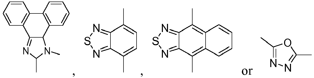
- More preferably, the host material has the following structures:


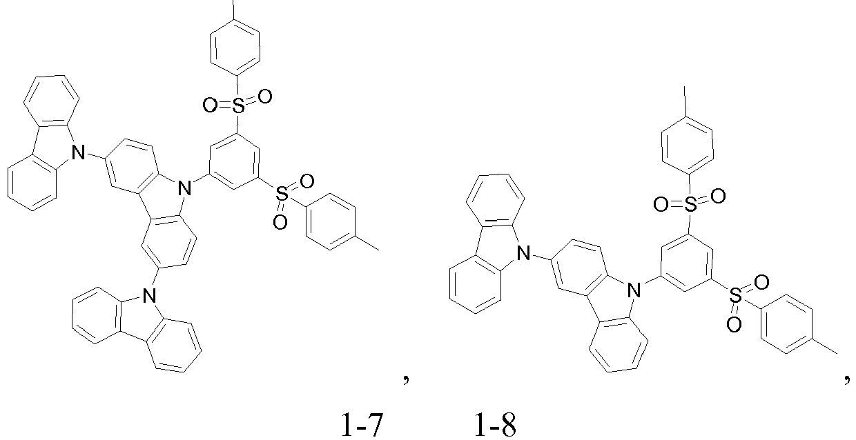


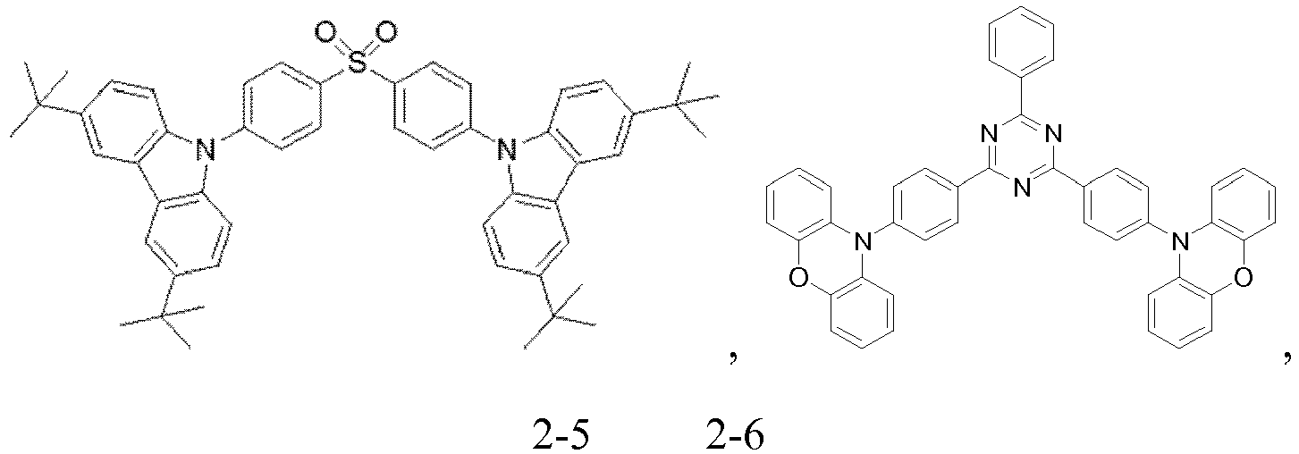


- Preferably, the luminescent dye is a fluorescent dye with the triplet state energy level lower than 2.3 eV. More preferably, the fluorescent dye is selected from coumarins or bipyranes.
- Preferably, the doping concentration of the fluorescent dye in the light-emitting layer is not greater than 5% by weight. Further preferably, the doping concentration of the fluorescent dye in the light-emitting layer is 0.001% to 1% by weight. More preferably, the doping concentration of the fluorescent dye in the light-emitting layer is 0.1 % to 1% by weight.
- Preferably, the triplet state energy level of the material of the hole transport layer is higher than that of the host material. Further preferably, the triplet state energy level of the material of the hole transport layer is higher than 2.5 eV. More preferably, the hole transport layer is made from a low-molecular material, for example, arylamines and/or branched polymers, and most preferably N,N'-diphenyl-N,N'-(1-naphthyl)-1,1'-biphenyl-4,4'-diamine.
- Preferably, the triplet state energy level of the material of the electron transport layer is higher than 2.5 eV.
- Preferably, a hole injection layer is provided between the anode and the hole transport layer. The hole injection layer is made from 4,4',4"-tris (3-methylphenylaniline) triphenylamine doped with F4TCNQ, or copper phthalocyanine, or metal oxide for example molybdenum oxide and rhenium oxide.
- The present invention provides a method for preparing the organic electroluminescent device, including: successively depositing an anode, a hole transport layer, a light-emitting layer, an electron transport layer and a cathode which are stacked; and then packaging the deposition.
- The present invention achieves the following technical effect:
- With the organic electroluminescent device according to the present invention, since a new host material in the light-emitting layer is used, which has both a donor group and an acceptor group, and the triplet state generated in the light-emitting layer may be fully utilized to achieve 100% of light-emitting efficiency in the fluorescent device. Furthermore, no noble metal is required, thus reducing the cost.
-
-
FIG. 1 is a schematic diagram illustrating energy transfer and light emitting of a light-emitting layer of an organic electroluminescent device made from a first type of material; -
FIG. 2 is a schematic diagram illustrating energy transfer and light emitting of a light-emitting layer of an organic electroluminescent device made from a second type of material; and -
FIG. 3 is a schematic basic structural diagram of an organic electroluminescent device according to the present invention. - Reference numerals and denotations thereof:
- 01: Substrate
- 02: Anode layer
- 03: Cathode layer
- 04: Hole injection layer
- 05: Hole transport layer
- 06: Light-emitting layer
- 07: Electron transport layer
- The present invention will be further described with reference to the accompany drawings and specific embodiments to make those skilled in the art better understand the present invention and put it into practice. However, the embodiments exemplified are not intended to limit the present invention.
- The organic electroluminescent device of the present invention includes an anode, a hole transfer layer, a light-emitting layer, an electron transport layer and a cathode, which are stacked, wherein the host material of the light-emitting layer is a material with a small difference in energy level (0 to 0.3 eV) between the triplet state of the CT excited state and the triplet state of the n-π excited state, and material with a great difference in energy level (more than 10 eV) between the two but the second triplet state of the n-π excited state slightly lower or higher than the first singlet state of the CT excited state (a difference of 0 to 0.1 eV between the two). The material selected or designed herein has both of donor groups and acceptor groups, which are spatially separated from each other, leading to spatial separation of HOMO energy level and LUMO energy level with reduced overlap integral. As a result, there is a small difference in energy level between the singlet state and the triplet state of the CT state of the material. Meanwhile, difference in energy level between the singlet state and the triplet state of phenanthroimidazolyl, naphthoimidazolyl, benzothiazolyl or anthryl which are selected herein is above 1.0 eV, and thus the requirements of the second type of material can also be met.
- The host material is preferably doped with a fluorescent dye, and the energy level of the singlet state of the fluorescent dye is lower than that of the CT state of the host material. The light-emitting wavelength of the fluorescent dye selected is longer than that of the host material, and thus the energy level of the singlet state of the dye may be promised to be lower than that of the host material. By doping with the fluorescent dye, the energy from the singlet state of the CT state of the host material may be directly transferred to the fluorescent dye. Radiation lifetime of the singlet state excitons of the CT state is shortened by the energy transfer, and thus the utilization efficiency of the triplet state of the CT state is enhanced to obtain high light-emitting efficiency.
- The concentration of the fluorescent dye is preferably lower than the mass concentration of 1%, and material with a relatively great overlapping between the absorption spectrum of the fluorescent dye and the body emission spectrum is preferred. In view of this, efficiency for energy transfer is enhanced, and meanwhile, Dexter energy transfer within short distance is reduced since excitons in this portion will be lost. Meanwhile, the triplet state energy level of the electron transport material and the hole transport material in the present invention is higher than that of the host material, which helps to confine excitons in the light-emitting layer. The triplet state energy level of the fluorescent dye in the present invention is lower than 2.3 eV, while the triplet state energy level of the electrons and holes is higher than 2.5 eV. Thus, the excitons in the light-emitting layer may be effectively confined.
- The light-emitting layer of the organic electroluminescent device of the present invention includes host material and a luminescent dye, the host material is material with charge-transfer transition, and the host material has both of a donor group unit and an acceptor group unit. The donor group unit is a group consisting of one donor group or more than two donor groups connected together; and the acceptor group unit is a group consisting of one acceptor group or more than two acceptor groups connected together.
- Specifically, the structure of the host material may be a donor-connection-acceptor structure or a donor-acceptor-donor structure or the like.
- The donor group is selected from indolocarbazolyl; carbazolyl; dicarbazyl; triphenylamine; phenoxazine; indolocarbazolyl substituted by more than one of C1-6 alkyl, methoxyl, ethyoxyl or phenyl; carbazolyl substituted by more than one of C1-6 alkyl, methoxyl, ethyoxyl or phenyl; dibenzofuryl substituted by more than one of C1-6 alkyl, methoxyl, ethyoxyl or phenyl; triphenylamine substituted by more than one of C1-6 alkyl, methoxyl, ethyoxyl or phenyl; or phenoxazine substituted by more than one of C1-6 alkyl, methoxyl, ethyoxyl or phenyl.
- The acceptor group is selected from naphthyl; anthryl; phenanthryl; pyrenyl; triazinyl; benzimidazolyl; cyano; pyridyl; sulfonyl; phenanthroimidazolyl; naphthoimidazolyl; benzothiazolyl; oxiadiazolyl; naphthyl substituted by more than one of C1-6 alkyl, methoxyl, ethyoxyl, phenyl or pyridyl; anthryl substituted by more than one of C1-6 alkyl, methoxyl, ethyoxyl, phenyl or pyridyl; phenanthryl substituted by more than one of C1-6 alkyl, methoxyl, ethyoxyl, phenyl or pyridyl; pyrenyl substituted by more than one of C1-6 alkyl, methoxyl, ethyoxyl, phenyl or pyridyl; triazinyl substituted by more than one of C1-6 alkyl, methoxyl, ethyoxyl, phenyl or pyridyl; benzimidazolyl substituted by more than one of C1-6 alkyl, methoxyl, ethyoxyl, phenyl or pyridyl; pyridyl substituted by more than one of C1-6 alkyl, methoxyl, ethyoxyl, phenyl or pyridyl; sulfonyl substituted by more than one of C1-6 alkyl, methoxyl, ethyoxyl, phenyl or pyridyl; phenanthroimidazolyl substituted by more than one of C1-6 alkyl, methoxyl, ethyoxyl, phenyl or pyridyl; naphthoimidazolyl substituted by more than one of C1-6 alkyl, methoxyl, ethyoxyl, phenyl or pyridyl; benzothiazolyl substituted by more than one of C1-6 alkyl, methoxyl, ethyoxyl, phenyl or pyridyl; and oxiadiazolyl substituted by more than one of C1-6 alkyl, methoxyl, ethyoxyl, phenyl or pyridyl.
- One or more of the donor group units are directly linked to one or more of the acceptor group units to form the host material; or one or more of the donor group units and one or more of the acceptor group units are respectively linked to a linking group to form the host material, the linking group being a group with steric hindrance.
- The linking group is selected from spiro-fluorenyl; phenyl; biphenylyl; spiro-fluorenyl substituted by at least one of C1-6 alkyl or phenyl; phenyl substituted by at least one of C1-6 alkyl or phenyl; or biphenylyl substituted by at least one of C1-6 alkyl or phenyl.
- The donor group is preferably selected from the following structures:


- The acceptor group is preferably selected from the following structures:


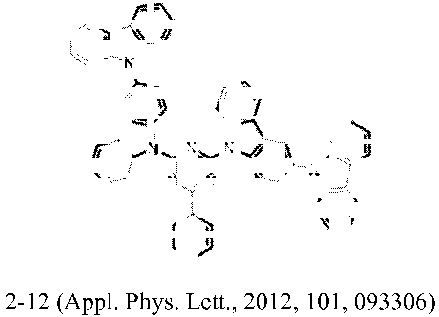
- Specifically, the host material is selected from compounds with the following structures:
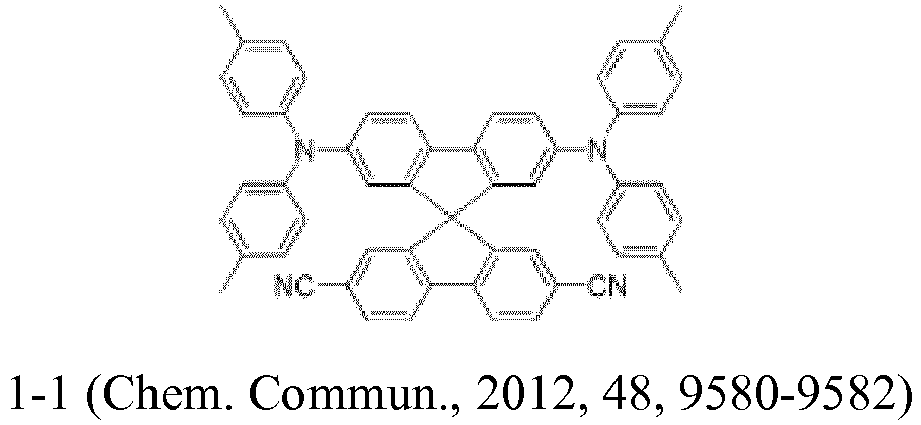




Gaussian 03/TD-DFT)
- Synthesis of related compounds in the application:
-

- 3.34 g of carbazole, 3.22 g of 3,6-dibromocarbazole, 0.5 g of CuI, 0.5 g of phenanthroline and 5.2 g of potassium carbonate were added into a 100-ml round-bottom flask; the mixture was added with 60 ml of DMF, and heated and refluxed under a nitrogen atmosphere for 48 hours; and the reaction solution was poured into water and vacuum filtered to obtain solids. The solids were separated by a chromatographic column to obtain 1-7a. The yield was 30%.
- Mass spectrometry data: ESI-MSm/z: 498[M+H]+; elemental analysis: C36H23N3:C86.90, H:4.66, N:8.44.
- 3.11 g of tribromobenzene, 2.48 g of methylthiophenol, 6 g of potassium carbonate and 1 g of copper iodide were added into a 100-ml round-bottom flask; the mixture was added with 50 ml of DMF, and heated under a nitrogen atmosphere for 24 hours; and the reaction solution was poured into water and vacuum filtered to obtain solids. The solids were separated by a chromatographic column to obtain 1-7b. The yield was 60%.
- Mass spectrometry data: ESI-MSm/z: 401[M+H]+; elemental analysis: C20H17BrS, C:59.85, H: 4.27.
- In an ice-water bath, 1-7b, which was dissolved in 30 ml, was slowly added dropwise into 1 g of mCPBA in dichloromethane solution, and completely added in the ice-water bath; and then the mixture was reacted for 12 hours. The solids were separated by a chromatographic column to obtain 1-7c. The yield was 99%.
- Mass spectrometry data: ESI-MSm/z: 465[M+H]+; elemental analysis: C20H17BrO4S2, C:86.90, H: 4.66, N: 8.44.
- 4.97 g of 1-7a, 4.63 g of 1-7b, 0.5 g of CuI, 0.5 g of phenanthroline and 5.2 g of potassium carbonate were added into a 100-ml round-bottom flask; the mixture was added with 60 ml of DMF, and heated and refluxed under a nitrogen atmosphere for 48 hours; and the reaction solution was poured into water and vacuum filtered to obtain solids. The solids were separated by a chromatographic column to obtain 1-7. The yield was 60%.
- Mass spectrometry data: ESI-MSm/z: 882[M+H]+; elemental analysis: C56H39N3O4S2, C 76.25, H 4.46, N 4.76.
- The synthesis of 1-4 may be referenced to the synthesis of 1-7, substance test data: mass spectrometry data: ESI-MSm/Z: 717[M+H]+; elemental analysis: C44H32N2O4S2, C 73.72, H 4.50, N 3.91.
-

- 4.52 g of 1-8 a, 3 g of 1-8b and 0.05 g of tetrakis(triphenylphosphine)palladium catalyst, as well as 5.4 g of potassium carbonate, were added into a round-bottom flask; and the mixture was added with 30 ml of methylbenzene, 20 ml of water and 5 ml of ethanol, and reacted at 85°C for 48 hours. The mixture was extracted with dichloromethane at the end of the reaction to obtain an organic layer, and then separated by a chromatographic column to obtain 1-8. The yield was 65%.
- Mass spectrometry data: ESI-MSm/z: 640[M+H]+; elemental analysis: C45H29N5, C 84.48, H 4.57, N 10.95.
-

- 2.43 g of 2-1a was added into 0.24 g of NaH in ultra-dry DMF solution (30 ml); the mixture was stirred at room temperature for 30 minutes; then 2.54 g of 2-1b in DMF solution was added dropwise to this solution, heated to 100°C, and stirred for 1 hour; the mixture was poured into water after being cooled; and solids were filtered and separated by a chromatographic column.2-1 was obtained.
- Mass spectrometry data: ESI-MSm/z: 701[M+H]+; elemental analysis: C48H32N2O2S, C 82.26, H 4.60, N 4.0.
- The synthesis of compound 2-2 may be referenced to the synthesis of 2-1. The method is basically the same as that of the compound 2-1, and the difference is that 2-1a is replaced by bicarbazolyl.
- Mass spectrometry data: ESI-MSm/z: 879[M+H]+; elemental analysis: C60H38N4O2S, C 81.98, H 4.36, N 6.37.
-

- 2.25 g of 2,4-dichloro-6-phenyl triazine, 2 g of 3-bromophenylboronic acid and 0.05 g of tetrakis(triphenylphosphine)palladium catalyst, as well as 5.4 g of potassium carbonate, were added into a round-bottom flask; and the mixture was added with 30 ml of methylbenzene, 20 ml of water and 5 ml of ethanol, and reacted at 85°C for 48 hours. The mixture was extracted with dichloromethane at the end of the reaction to obtain an organic layer, and then separated by a chromatographic column to obtain 2-7a. The yield was 58%.
- Mass spectrometry data: ESI-MSm/z: 466[M+H]+; elemental analysis: C21H13Br2N3, C 53.99, H 2.80, N 8.99.
- 4.65 g of 2-7a, 3.66 g of phenoxazine, 0.5 g of CuI, 0.5 g of phenanthroline and 5.2 g potassium carbonate were added into a 100-ml round-bottom flask; the mixture was added with 60 ml of DMF, and heated and refluxed under a nitrogen atmosphere for 48 hours; and the reaction solution was poured into water and vacuum filtered to obtain solids. The solids were separated by a chromatographic column to obtain 2-7. The yield was 48%.
- Mass spectrometry data: ESI-MSm/z: 672[M+H]+; elemental analysis: C45H29N5O2, C:80.46, H: 4.35, N: 4.76.
- 2.25 g of 2,4-dichloro-6-phenyl triazine, 2 g of 4-bromophenylboronic acid and 0.05 g of tetrakis(triphenylphosphine)palladium catalyst, as well as 5.4 g of potassium carbonate, were added into a round-bottom flask; and the mixture was added with 30 ml of methylbenzene, 20 ml of water and 5 ml of ethanol, and reacted at 85°C for 48 hours. The mixture was extracted with dichloromethane at the end of the reaction to obtain an organic layer, and then separated by a chromatographic column to obtain 2-8a. The yield was 55%.
- Mass spectrometry data: ESI-MSm/z: 466[M+H]+; elemental analysis: C21H13Br2N3, C 53.99, H 2.80, N 8.99.
- 4.65 g of 2-8a, 3.66 g of phenoxazine, 0.5 g of CuI, 0.5 g of phenanthroline and 5.2 g potassium carbonate were added into a 100-ml round-bottom flask; the mixture was added with 60 ml of DMF, and heated and refluxed under a nitrogen atmosphere for 48 hours; and the reaction solution was poured into water and vacuum filtered to obtain solids. The solids were separated by a chromatographic column to obtain 2-8. The yield was 56%.
- Mass spectrometry data: ESI-MSm/z: 640[M+H]+; elemental analysis: C45H29N5, C 84.48, H 4.57, N 10.95.
- The synthesis of 2-9 may be referenced to the synthesis of 2-7, and the difference is that different donor groups were used, and the phenoxazine was replaced by carbazole.4.65 g of 2-8a, 3.0 g of carbazole, 0.5 g of CuI, 0.5 g of phenanthroline and 5.2 g potassium carbonate were added into a 100-ml round-bottom flask; the mixture was added with 60 ml of DMF, and heated and refluxed under a nitrogen atmosphere for 48 hours; and the reaction solution was poured into water and vacuum filtered to obtain solids. The solids were separated by a chromatographic column to obtain 2-9. The yield was 50%.
- Mass spectrometry data: ESI-MSm/z: 640[M+H]+; elemental analysis: C45H29N5, C 84.48, H 4.57, N 10.95.
-

- 3.32 g of phenylindole carbazole, 2.67 g of 2-chloro-4,6-diphenyl triazine, 0.5 g of CuI, 0.5 g of phenanthroline and 5.2 g of potassium carbonate were added into a 100-ml round-bottom flask; the mixture was added with 60 ml of DMF, and heated and refluxed under a nitrogen atmosphere for 48 hours; and the reaction solution was poured into water and vacuum filtered to obtain solids. The solids were separated by a chromatographic column to obtain 2-7. The yield was 48%.
- Mass spectrometry data: ESI-MSm/z: 564[M+H]+; elemental analysis: C39H25N5, C 83.10, H 4.47, N 12.43.
-

- 3 ml of pyridine was added to a mixed solution of o-phenylenediamine (0.6g) and sulfoxide chloride (5 ml), and stirred at 60°C for 10 hours; and the mixture was extracted with dichloromethane and washed with a great amount of water to obtain solids.
- Mass spectrometry data: ESI-MSm/z: 205.
- 2.25 g of 3-3a, 2 g of phenylboronic acid and 0.05 g of tetrakis(triphenylphosphine)palladium catalyst and 5.4 g of potassium carbonate were added into a round-bottom flask; the mixture was added with 30 ml of methylbenzene, 20 ml of water and 5 ml of ethanol, and reacted at 85°C for 48 hours. The mixture was extracted with dichloromethane at the end of the reaction to obtain an organic layer, and then separated by a chromatographic column to obtain 3-3a. The yield was 58%.
- Mass spectrometry data: ESI-MSm/z: 246[M+H]+
- 2.46 g of 3-3b, 2.39 g of 4-(diphenylamino)phenylboronic acid, 0.05 g of tetrakis(triphenylphosphine)palladium catalyst and 5.4 g of potassium carbonate were added into a round-bottom flask; the mixture was added with 30 ml of methylbenzene, 20 ml of water and 5 ml of ethanol, and reacted at 85°C for 48 hours; and the mixture was extracted with dichloromethane at the end of the reaction to obtain an organic layer, and then separated by a chromatographic column to obtain 3-3a. The yield was 58%.
- Mass spectrometry data: ESI-MSm/z: 456[M+H]+; elemental analysis: C30H24N3S, C 79.09, H 4.65, N 9.22.
- The synthesis of compound 3-4 may be referenced to the synthesis of compound 3-3. The steps are basically the same, and the difference is that the acceptor groups are thiophene-substituted benzothiazole.
- Mass spectrometry data: ESI-MSm/z: 462[M+H]+; elemental analysis: C28H19N3S2: C: 72.86, H: 4.15, N: 9.10.
- The synthesis of compound 3-5 may be referenced to the synthesis of compound 3-3. The steps are basically the same, and the difference is that the acceptor groups are thiophene-substituted naphthothiazole.
- Mass spectrometry data: ESI-MSm/z: 512[M+H]+; elemental analysis: C32H21N3S2: C: 75.12, H: 4.15, N: 8.21.
- Embodiment of the organic light-emitting display device of the present invention: the anode may be inorganic material or organic conducting polymer. The inorganic material is generally metal oxide (for example, indium tin oxide (ITO), zinc oxide (ZnO), indium zinc oxide (IZO) or the like) or metal with a relatively high work function (for example, gold, copper, silver), and is preferably ITO; and the organic conducting polymer is preferably one of polythiophene/polyvinyl benzenesulfonate (hereinafter, PEDOT/PSS for short) and polyaniline (hereinafter, PANI for short).
- The cathode is generally metal with a relatively low work function (for example, lithium, magnesium, calcium, strontium, aluminum, indium or the like, or the ir alloys with copper, gold, and silver) or an electrode layer alternately formed of metal and metal fluorides. The cathode in the present invention is preferably an LiF layer and an Al layer which are stacked (with the LiF layer being on the outer side).
- The hole transport layer may be made from a low-molecular material, for example, arylamines and/or branched polymers, and is preferably NPB.
- The fluorescent dye is preferably selected from coumarin compounds (for example, DMQA, C545T) or bipyrane compounds (for example DCJTB, DCM), or the like.
- The electron transport layer may be made from an organic metal complexe (for example, Alq3, Gaq3, BAlq or Ga(Saph-q)) or other materials commonly used in the electron transport layer, for example aromatic fused ring compounds (for example, pentacene, perylene) or o-phenanthroline compounds (for example, Bphen, BCP).
- With regard to the organic electroluminescent device of the present invention, a hole injection layer can also be provided between the anode and the hole transport layer, and the hole injection layer may be made from 4,4',4"-tri(3-methyl phenylaniline) triphenylamine doped with F4TCNQ, or may be CuPc, or may be metal oxides (for example, molybdenum oxide, rhenium oxide).
- The thickness of each layer described above may be a common thickness of these layers in the prior art.
- The present invention also provides a method for manufacturing the organic electroluminescent device, as shown in
FIG. 3 , including: successively depositing, on asubstrate 01, ananode 02, ahole transport layer 05, a light-emittinglayer 06, anelectron transport layer 07 and acathode 03 which are stacked; then packaging the deposition wherein the difference in energy level between the triplet state and the singlet state of the host material in the light-emittinglayer 06 is lower than 0.15 eV. - The substrate may be glass or a flexible substrate, and the substrate may be made from a polyester compound material, polyimide compound material or a thin metal sheet. The stacking and the packaging may be performed by any suitable method well known to those skilled in the art.
- The present invention will be further described by embodiments.
- For the purpose of convenience, the abbreviations and full names of some organic materials involved in this description are all listed below:
Abbreviation Full name Structural formula Alq3 Tris(8-Hydroxyquinoline) aluminum 
BAlq Bis(2-methyl-8-quinolyl)-4-phenyl-phenol aluminum (□) 
BCP 2,9-dimethyl-4,7-diphenyl-1 ,10-o-phenanthroline 
Bphen 4,7-diphenyl-1,10-o-phenant hroline 
C545T 10-(2-benzothiazole)-1,1,7,7 -tetramethyl-2,3,6,7-tetrahy dro-1H,5H,11H-benzo[1]py ran[6,7-8-i,j]quinolizin 
CBP 4,4'-N,N'-dicarbazole-biphe nyl 
CPF 9,9-bis (4-dicarbazole-phenyl) fluorene 
MTDATA 4,4',4"-tris (3-methylphenylamine) triphenylamine 
NPB N,N'-bis-(1-naphthyl)-N,N' -diphenyl-1,1'-biphenyl-4,4' -diamine 
PBD 2-(4-tert-butylphenyl)-5-(4-biphenyl)-1,3,4-oxadiazole 
pentacene pentacene 
TPD N,N'-diphenyl-N,N'-Bis(3-methylphenyl)-1,1'-bipheny 1-4,4'-diamine 
perylene Perylene 
DCJTB 4-4-dicyanomethylene-2-t-b utyl-6-(1,1,7,7-tetramethyl-j ulolidyl-9-enyl)-4H-pyran 
DCM 4-dicyanomethylene-2-meth yl-6-(p-dimethylaminostyryl )-4H-pyran 
rubrene 5,6,11,12-tetraphenylnaphth acene 
DCM-1 - 
DMQA 
F4TCNQ 
- In the following embodiments, the light-emitting efficiency of the device is tested by a test device consisting of keithley 2602 and a corrected silicon photodiode. Dividing the brightness obtained by the test device by the current density is the light-emitting efficiency. The luminescence spectrum is tested by Pr655.
- Yellow light-emitting devices with different doping concentrations of the fluorescent dye are manufactured in this embodiment, and these devices have structures shown in
FIG. 3 . The light-emitting layer contains one host material (Host1) and one fluorescent dye (YD1) for doping, wherein the Host 1 material is the first type of host material having a first triplet state of the (n-π) excited state thereof slowly lower than that of the CT excited state (0.1 eV), and the singlet state energy level of YD 1 is 2.2 eV, which is lower than that of the Host 1Host1 and YD1 respectively have the following structural formulas:
- The devices of the embodiment have the following structure:
- ITO (150nm)/NPB(40 nm)/Host 1 (0.01%, 0.5%, 1.0%, 5%): YD 1 (30nm)/Alq3(20nm)/LiF(0.5nm)/Al(150nm)
- wherein the percentages in the brackets before YD 1 represent different doping concentrations of the fluorescent dye; and in this embodiment and the description below, the doping concentration is represented by percentage by weight.
- The specific method for manufacturing the organic electroluminescent device is as follows.
- First, a glass substrate is cleaned with a detergent and deionized water, and the glass substrate is dried under an infrared lamp; and a layer of anode material is sputtered on the glass, with a film thickness of 150 nm.
- Then, the glass substrate with an anode is put in a vacuum chamber, and evacuated to 1×10⁻⁴ Pa; NPB is continuously evaporated on the anode layer film as a hole transport layer, with a film formation rate of 0.1 nm/s and an evaporated film thickness of 40 nm.
- A light-emitting layer is evaporated on the hole transport layer by double-source co-evaporation; and the mass percentages of Host1 and YD1 is controlled by a film thickness monitor by adjusting the film formation rate. The evaporated film thickness is 30 nm.
- A layer of Alq3 material is continuously evaporated on the light-emitting layer as an electron transport layer, with an evaporation rate of 0.1 nm/s and an overall evaporated film thickness of 20 nm.
- Finally, an LiF layer and an Al layer are successively evaporated on the light-emitting layer as the cathode layer of the device, wherein the evaporation rate of the LiF layer is 0.01 nm/s to 0.02 nm/s and the thickness is 0.5 nm, and the evaporation rate of the Al layer is 1.0 nm/s and the thickness is 150 nm.
- Organic electroluminescent device are manufactured by the same method as in Embodiment 1, and the devices have the following structure:
- ITO (150nm) /NPB (40 nm) /Host 1 (01%, 0.5%, 1.0%, 5%): YD 1 (30nm)/Alq3 (20nm) /LiF (0.5nm) /Al (150 nm).
- That is, the host material in the light-emitting layer of the device is AND without CT state transition.

- Performances of the organic electroluminescent devices of the Embodiment 1 and the Comparative Example 1 are listed in Table 1 below.
Table 1 Device Composition of the light-emitting layer Light-emitting efficiency Embodim ent 1 Host 1 (2-7): (0.01%) YD 1 (30 nm) 15.5 Host 1 (2-7): (0.5%) YD 1 (30 nm) 20.5 Host 1 (2-7): (1.0%) YD 1 (30 nm) 19.5 Host 1 (2-7): (5.0%) YD 1 (30 nm) 8.3 Comparati ve Example 1 ADN: (0.01%) YD 1 (30 nm) 4.1 ADN: (0.5%) YD 1 (30 nm) 5.2 ADN: (1.0%) YD 1 (30 nm) 5.9 ADN: (5.0%) YD 1 (30 nm) 4.6 - It may be seen from Table 1 that, with a same doping concentration of a fluorescent dye, the light-emitting efficiency of the light-emitting devices manufactured by using the first type of host material in which the first triplet state of the (n-π) excited state is slightly lower than that of the CT excited state (0.1 eV) is obviously higher than that of the light-emitting devices manufactured by using host material without the CT state.
- In addition, when the doping concentration of the fluorescent dye is between 0.5% and 1%, high light-emitting efficiency may be particularly obtained.
- Red light-emitting devices with different doping concentrations of fluorescent dyes are manufactured in this embodiment, and these devices have structures shown in
FIG. 3 . The light-emitting layer contains one host material (Host 2) and one fluorescent doping dye (RD 1),wherein there is a great difference in energy level between the triplet state of the CT excited state and the triplet state of the (n-π) excited state of the Host 2, and the second triplet state of the (n-π) excited state is higher than the first singlet state of the CT state thereof; the singlet state energy lever of RD 1 is 2.0 eV, and the singlet state energy level of RD 1 is lower than that of Host 2. Host 1 and RD 1 have the following structural formulas:
- Organic electroluminescent devices are manufactured by the same method as in Embodiment 1, and the devices have the following structure:
- ITO (150nm) /NPB (40 nm) /Host 2 (0.01%, 0.5%, 1.0%, 5%): RD 1 (30nm)/Bphen(20nm) /LiF (0.5nm) /Al (150 nm)
- wherein the percentages in the baskets before RD 1 represent different doping concentrations of the fluorescent dye.
- Organic electroluminescent devices are manufactured by the same method as in Embodiment 1, and the devices have the following structure:
- ITO (150nm)/NPB 40 nm)/Alq3: (0.01%, 0.5%, 1.0%, 5%, 10%) RD 1 (30nm)/Bphen (20nm)/LiF (0.5nm)/Al (150 nm).
- That is, Alq3 is used as the host material of the light-emitting layer, without CT state transition.
- Performances of the organic electroluminescent devices of the embodiments and the Comparative Example 2 are listed in Table 2 below.
Table 2 Device Composition of the light-emitting layer Light-emitting efficiency Embodiment 2 Host 2 (3-6): (0.01%) RD 1 (30 nm) 5.0 Host 2 (3-6): (0.5%) RD 1 (30 nm) 6.6 Host 2 (3-6): (1.0%) RD 1 (30 nm) 5.9 Host 2 (3-6): (5.0%) RD 1 (30 nm) 4.2 Host 2 (3-6): (10.0%) RD 1 (30 nm) 2.1 Comparative Example 2 Alq3: (0.01%) RD 1 (30 nm) 0.4 Alq3: (0.5%) RD 1 (30 nm) 2.2 Alq3: (1.0%) RD 1 (30 nm) 2.3 Alq3: (5.0%) RD 1 (30 nm) 1.2 Alq3: (10.0%) RD 1 (30 nm) 0.7 - It may be seen from Table 2 that with a same doping concentration, the light-emitting efficiency of the light-emitting devices manufactured by using manufactured by adopting host material in which there is a great difference (1.3 eV) in the energy level (1.3 eV) between the triplet state of the CT excited state and the triplet state of the (n-π) exited state and the second triplet state of the (n-π) excited state is higher than the first singlet state of the CT excited state thereof, is obviously higher than that of the by adopting organic electroluminescent devices using the common host material. In addition, when the doping concentration of the fluorescent dye is between 0.01% and 1%, particularly, a high light-emitting efficiency may be particularly obtained.
- In order to test then influence of the host material of the present invention on the performance of the electroluminescent devices, in this embodiment, organic electroluminescent devices are manufactured by the same method as in Embodiment 1, and the light-emitting devices have the following structure:
- ITO (150 nm) /NPB (40 nm)/host material: 0.5% YD 1 (30 nm)/Bphen (20 nm) /LiF (0.5 nm) /Al (150 nm).
- Performances of the organic electroluminescent devices are represented in Table 3 below.
Table 3 Structure of the light-emitting layer Current efficiency cd/A OLED 3 1-1: (0.5%) YD 1 (30 nm) 20 OLED 4 1-2: (0.5%) YD 1 (30 nm) 24 OLED 5 1-3: (0.5%) YD 1 (30 nm) 30 OLED 6 1-4: (0.5%) YD 1 (30 nm) 24 OLED 7 1-5: (0.5%) YD 1 (30 nm) 34 OLED 8 1-6: (0.5%) YD 1 (30 nm) 36 OLED 9 1-7: (0.5%) YD 1 (30 nm) 28 OLED 10 1-8: (0.5%) YD 1 (30 nm) 31 OLED 11 1-9: (0.5%) YD 1 (30 nm) 29 OLED 12 1-10: (0.5%) YD 1 (30 nm) 19 OLED 13 1-11: (0.5%) YD 1 (30 nm) 17 OLED 14 1-12: (0.5%) YD 1 (30 nm) 23 OLED 15 2-1: (0.5%) YD 1 (30 nm) 19 OLED 16 2-2: (0.5%) YD 1 (30 nm) 36 OLED 17 2-3: (0.5%) YD 1 (30 nm) 28 OLED 18 2-4: (0.5%) YD 1 (30 nm) 24 OLED 19 2-5: (0.5%) YD 1 (30 nm) 35 OLED 20 2-6: (0.5%) YD 1 (30 nm) 12 OLED 21 2-7: (0.5%) YD 1 (30 nm) 20.5 OLED 22 2-8: (0.5%) YD 1 (30 nm) 33 OLED 23 2-9: (0.5%) YD 1 (30 nm) 32 OLED 24 2-10: (0.5%) YD 1 (30 nm) 27 OLED 25 2-11: (0.5%) YD 1 (30 nm) 25 OLED 26 2-12: (0.5%) YD 1 (30 nm) 36 OLED 27 2-13: (0.5%) YD 1 (30 nm) 35 OLED 28 2-14: (0.5%) YD 1 (30 nm) 35 OLED 29 2-15: (0.5%) YD 1 (30 nm) 31 OLED 30 3-1: (0.5%) YD 1 (30 nm) 23 OLED 31 3-2: (0.5%) YD 1 (30 nm) 21 OLED 32 3-3: (0.5%) YD 1 (30 nm) 25 OLED 33 3-4: (0.5%) YD 1 (30 nm) 16 OLED 34 3-5: (0.5%) YD 1 (30 nm) 14 OLED 35 3-6: (0.5%) YD 1 (30 nm) 11 - The aforementioned embodiments are merely preferred embodiments exemplified for fully describing the present invention and the protection scope of the present invention is not limited thereto. Equivalent replacements or changes made on the basis of the present invention by those skilled in the prior art are included in the protection scope of the present invention. The protection scope of the present invention is subject to the appended claims.
Claims (18)
- An organic electroluminescent device, comprising an anode, a hole transport layer, a light-emitting layer, an electron transport layer and a cathode which are stacked, the light-emitting layer comprising a host material and a luminescent dye, characterized in that:the host material of the light-emitting layer is a material in which the triplet state energy level in CT excited state is higher than that in the n-π excited state by 0 to 0.3 eV; orthe host material of the light-emitting layer is a material in which the triplet state energy level in CT excited state is higher than that in an n-π excited state by more than 1.0 eV, and the difference between the second triplet state energy level in the n-π excited state of the host material and a first singlet state energy level in the CT excited state is -0.1 to 0.1 eV; andthe luminescent dye is a fluorescent dye.
- The organic electroluminescent device according to claim 1, characterized in that the energy gap of the singlet state and the triplet state of the host material of the light-emitting layer is 0 to 0.3 eV.
- The organic electroluminescent device according to claim 1, characterized in that the singlet state energy level of the fluorescent dye is lower than that of the host material.
- The organic electroluminescent device according to claim 1, characterized in that the host material is a material with charge-transfer transition, and the host material has both a donor group unit and an acceptor group unit;
the donor group unit is a group consisting of one donor group or more than two donor groups connected together;
the acceptor group unit is a group consisting of one acceptor group or more than two acceptor groups connected together;
the donor group is selected from indolocarbazolyl; carbazolyl; dicarbazyl; triphenylamine; phenoxazine; indolocarbazolyl substituted by more than one of C1-6 alkyl, methoxyl, ethyoxyl or phenyl; carbazolyl substituted by more than one of C1-6 alkyl, methoxyl, ethyoxyl or phenyl; dicarbazyl substituted by more than one of C1-6 alkyl, methoxyl, ethyoxyl or phenyl; triphenylamine substituted by more than one of C1-6 alkyl, methoxyl, ethyoxyl or phenyl; or phenoxazine substituted by more than one of C1-6 alkyl, methoxyl, ethyoxyl or phenyl;
the acceptor group is selected from naphthyl; anthryl; phenanthryl; pyrenyl; triazinyl; benzimidazolyl; cyano; pyridyl; sulfonyl; phenanthroimidazolyl; naphthoimidazolyl; benzothiazolyl; oxiadiazolyl; naphthyl substituted by more than one of C1-6 alkyl, methoxyl, ethyoxyl, phenyl or pyridyl; anthryl substituted by more than one of C1-6 alkyl, methoxyl, ethyoxyl, phenyl or pyridyl; phenanthryl substituted by more than one of C1-6 alkyl, methoxyl, ethyoxyl, phenyl or pyridyl; pyrenyl substituted by more than one of C1-6 alkyl, methoxyl, ethyoxyl, phenyl or pyridyl; triazinyl substituted by more than one of C1-6 alkyl, methoxyl, ethyoxyl, phenyl or pyridyl; benzimidazolyl substituted by more than one of C1-6 alkyl, methoxyl, ethyoxyl, phenyl or pyridyl; pyridyl substituted by more than one of C1-6 alkyl, methoxyl, ethyoxyl, phenyl or pyridyl; sulfonyl substituted by more than one of C1-6 alkyl, methoxyl, ethyoxyl, phenyl or pyridyl; phenanthroimidazolyl substituted by more than one of C1-6 alkyl, methoxyl, ethyoxyl, phenyl or pyridyl; naphthoimidazolyl substituted by more than one of C1-6 alkyl, methoxyl, ethyoxyl, phenyl or pyridyl; benzothiazolyl substituted by more than one of C1-6 alkyl, methoxyl, ethyoxyl, phenyl or pyridyl; and oxiadiazolyl substituted by more than one of C1-6 alkyl, methoxyl, ethyoxyl, phenyl or pyridyl;
wherein one or more of the donor group units are directly linked to one or more of the acceptor group units to form the host material; or one or more of the donor group units and one or more of the acceptor group units are respectively linked to a linking group to form the host material, the linking group being a group with steric hindrance. - The organic electroluminescent device according to claim 4, characterized in that one or two donor group units and one or two acceptor group units are respectively linked to a linking group to form the host material; or one or two acceptor group units are directly linked to one or two donor group units to form the host material.
- The organic electroluminescent device according to claim 4, characterized in that the linking group is selected from spiro-fluorenyl; phenyl; biphenylyl; spiro-fluorenyl substituted by at least one of C1-6 alkyl or phenyl; phenyl substituted by at least one of C1-6 alkyl or phenyl; or biphenylyl substituted by at least one of C1-6 alkyl or phenyl.
- The organic electroluminescent device according to claim 4, characterized in that the donor group is selected from the following groups:


- The organic electroluminescent device according to claim 4, characterized in that the acceptor group is selected from the following groups:


- The organic electroluminescent device according to claim 4, characterized in that the host material has the following structures:


- The organic electroluminescent device according to claim 1, characterized in that the luminescent dye is a fluorescent dye with triplet state energy level lower than 2.3 eV.
- The organic electroluminescent device according to claim 10, characterized in that the doping concentration of the fluorescent dye in the light-emitting layer is not greater than 5% by weight.
- The organic electroluminescent device according to claim 11, characterized in that the doping concentration of the fluorescent dye in the light-emitting layer is 0.001 % to 1% by weight.
- The organic electroluminescent device according to claim 11, characterized in that the doping concentration of the fluorescent dye in the light-emitting layer is 0.1 % to 1% by weight.
- The organic electroluminescent device according to claim 1, characterized in that the triplet state energy level of the material of the hole transport layer is higher than that of the host material.
- The organic electroluminescent device according to claim 1, characterized in that the triplet state energy level of the material of the hole transport layer is higher than 2.5 eV.
- The organic electroluminescent device according to claim 1, characterized in that the triplet state energy level of the material of the electron transport layer is higher than 2.5 eV.
- The organic electroluminescent device according to claim 1, characterized in that a hole injection layer is provided between the anode and the hole transport layer.
- A method for preparing the organic electroluminescent device according to claim 1, comprising: successively depositing an anode, a hole transport layer, a light-emitting layer, an electron transport layer and a cathode on a substrate, which are stacked; and then packaging.
Applications Claiming Priority (2)
| Application Number | Priority Date | Filing Date | Title |
|---|---|---|---|
| CN201310692266.2A CN104716268B (en) | 2013-12-17 | 2013-12-17 | A kind of organic electroluminescence device and preparation method thereof |
| PCT/CN2014/093904 WO2015090177A1 (en) | 2013-12-17 | 2014-12-16 | Organic electroluminescent device and method for manufacture thereof |
Publications (3)
| Publication Number | Publication Date |
|---|---|
| EP3070757A1 true EP3070757A1 (en) | 2016-09-21 |
| EP3070757A4 EP3070757A4 (en) | 2016-12-21 |
| EP3070757B1 EP3070757B1 (en) | 2019-05-08 |
Family
ID=53402101
Family Applications (1)
| Application Number | Title | Priority Date | Filing Date |
|---|---|---|---|
| EP14872476.8A Active EP3070757B1 (en) | 2013-12-17 | 2014-12-16 | Organic electroluminescent device and method for manufacture thereof |
Country Status (7)
| Country | Link |
|---|---|
| US (1) | US10312453B2 (en) |
| EP (1) | EP3070757B1 (en) |
| JP (1) | JP6581585B2 (en) |
| KR (1) | KR101930146B1 (en) |
| CN (1) | CN104716268B (en) |
| TW (1) | TWI553938B (en) |
| WO (1) | WO2015090177A1 (en) |
Families Citing this family (37)
| Publication number | Priority date | Publication date | Assignee | Title |
|---|---|---|---|---|
| KR20120100709A (en) | 2010-01-15 | 2012-09-12 | 이데미쓰 고산 가부시키가이샤 | Organic electroluminescent element |
| JP2017212024A (en) * | 2014-08-28 | 2017-11-30 | 出光興産株式会社 | Organic electroluminescence device and electronic device |
| WO2016051309A1 (en) * | 2014-09-30 | 2016-04-07 | Semiconductor Energy Laboratory Co., Ltd. | Light-emitting element, display device, electronic device, and lighting device |
| CN107004777B (en) * | 2014-12-04 | 2019-03-26 | 广州华睿光电材料有限公司 | Polymers, mixtures, compositions, organic electronic devices containing the same, and monomers thereof |
| CN106328816B (en) * | 2015-06-16 | 2018-11-13 | 昆山国显光电有限公司 | A kind of organic electroluminescence device and preparation method thereof |
| US10700288B2 (en) * | 2015-07-24 | 2020-06-30 | Semiconductor Energy Laboratory Co., Ltd. | Light-emitting element, light-emitting device, electronic device, lighting device, and lighting system |
| KR101820208B1 (en) * | 2015-10-16 | 2018-01-18 | 성균관대학교산학협력단 | Organic light emitting material and organic light emitting device having the organic light emitting material |
| KR102458043B1 (en) * | 2015-11-25 | 2022-10-24 | 엘지디스플레이 주식회사 | Organic Light Emitting Diode Device |
| WO2017093843A1 (en) * | 2015-12-01 | 2017-06-08 | Semiconductor Energy Laboratory Co., Ltd. | Light-emitting element, light-emitting device, electronic device, and lighting device |
| CN106892857B (en) * | 2015-12-18 | 2020-02-18 | 昆山国显光电有限公司 | Thermally Activated Delayed Fluorescent Materials and Their Applications in Organic Electroluminescent Devices |
| CN105523991B (en) * | 2015-12-22 | 2018-05-01 | 吉林奥来德光电材料股份有限公司 | A kind of new carbazole compound and its preparation method and application |
| CN105399696B (en) * | 2015-12-25 | 2019-12-24 | 上海天马有机发光显示技术有限公司 | Organic electroluminescence compound and its organic optoelectronic device |
| CN105541824B (en) * | 2015-12-25 | 2019-07-05 | 上海天马有机发光显示技术有限公司 | Organic electroluminescent compounds and its organic photoelectric device |
| CN106920884B (en) * | 2015-12-25 | 2019-08-16 | 昆山工研院新型平板显示技术中心有限公司 | A kind of organic electroluminescence device |
| CN106920883B (en) * | 2015-12-25 | 2019-01-08 | 昆山工研院新型平板显示技术中心有限公司 | A kind of organic electroluminescence device |
| CN107056770A (en) * | 2016-04-25 | 2017-08-18 | 中节能万润股份有限公司 | A kind of compound as core using nitrogenous five-ring heterocycles and its application on organic electroluminescence device |
| CN106467531B (en) * | 2016-08-19 | 2019-04-19 | 江苏三月光电科技有限公司 | A kind of compound with nitrogen-containing five-membered heterocycle as core and application thereof |
| JP6803727B2 (en) * | 2016-09-23 | 2020-12-23 | 日本放送協会 | Organic electroluminescence element |
| CN106701063B (en) * | 2016-12-19 | 2019-05-14 | 三峡大学 | A controllable organic solid-state light-emitting material, preparation method and application thereof |
| CN108264479B (en) * | 2016-12-30 | 2023-10-27 | 昆山国显光电有限公司 | An organic electroluminescent device |
| US10784456B2 (en) * | 2017-06-06 | 2020-09-22 | Joled Inc. | Organic electroluminescent unit |
| KR102450436B1 (en) * | 2017-08-01 | 2022-10-04 | 삼성디스플레이 주식회사 | Heterocyclic compound and organic electroluminescence device including the same |
| KR102497284B1 (en) * | 2017-12-18 | 2023-02-08 | 삼성디스플레이 주식회사 | Organic light emitting device |
| CN109994634B (en) | 2017-12-29 | 2020-12-11 | 昆山国显光电有限公司 | Organic Electroluminescent Devices |
| CN110492008B (en) * | 2018-05-14 | 2020-06-12 | 江苏三月光电科技有限公司 | Thermal activation delayed fluorescence organic electroluminescent device |
| CN108695440B (en) * | 2018-05-30 | 2019-07-16 | 昆山国显光电有限公司 | A kind of organic electroluminescence device |
| US11063224B2 (en) | 2018-05-30 | 2021-07-13 | Kunshan Go-Visionox Opto-Electronics Co., Ltd. | Organic electroluminescent device |
| CN111372918B (en) | 2018-07-27 | 2023-09-05 | 出光兴产株式会社 | Compound, material for organic electroluminescent element, organic electroluminescent element, and electronic device |
| CN109096279B (en) * | 2018-09-28 | 2020-11-03 | 武汉天马微电子有限公司 | Nitrogen heterocyclic compound, display panel and display device |
| KR102796864B1 (en) * | 2019-08-30 | 2025-04-17 | 삼성전자주식회사 | Organic light emitting device |
| CN112054129B (en) | 2020-09-15 | 2024-04-09 | 京东方科技集团股份有限公司 | Light emitting device and display device |
| CN112701231B (en) * | 2020-12-31 | 2022-09-13 | 昆山国显光电有限公司 | Organic electroluminescent device and display device |
| JP2022112591A (en) * | 2021-01-22 | 2022-08-03 | キヤノン株式会社 | Organic light-emitting element, display device, imaging apparatus, electronic device, lighting device, and mobile body |
| CN113321677B (en) * | 2021-06-30 | 2023-05-05 | 京东方科技集团股份有限公司 | Thermal-activation delay fluorescent material, organic light-emitting device and display device |
| CN113851595B (en) * | 2021-09-27 | 2023-05-23 | 京东方科技集团股份有限公司 | Organic electroluminescent device and display device |
| CN115093380B (en) * | 2022-06-30 | 2023-06-20 | 江西科技师范大学 | A kind of benzothiadiazole derivative and its preparation method and application |
| CN115974861A (en) * | 2022-12-26 | 2023-04-18 | 苏州奥为光电新材料有限公司 | A thermally activated delay material of triazine derivatives and its preparation method and application |
Family Cites Families (24)
| Publication number | Priority date | Publication date | Assignee | Title |
|---|---|---|---|---|
| DE502005002342D1 (en) | 2005-03-15 | 2008-02-07 | Novaled Ag | Light-emitting component |
| JP2007027620A (en) | 2005-07-21 | 2007-02-01 | Konica Minolta Holdings Inc | Organic electroluminescence element, liquid crystal display and lighting system |
| US20080284318A1 (en) * | 2007-05-17 | 2008-11-20 | Deaton Joseph C | Hybrid fluorescent/phosphorescent oleds |
| JP2011026289A (en) * | 2009-06-25 | 2011-02-10 | Tosoh Corp | Amine compound and application thereof |
| CN101993440B (en) | 2009-08-25 | 2012-07-25 | 中国科学院化学研究所 | Benzothiadiazole-based multi-arm conjugated molecules as well as preparation method and application thereof |
| EP2492985A4 (en) | 2009-10-23 | 2017-03-29 | Hodogaya Chemical Co., Ltd. | Organic electroluminescent element |
| WO2011148909A1 (en) * | 2010-05-24 | 2011-12-01 | 出光興産株式会社 | Organic electroluminescent element |
| KR101906284B1 (en) * | 2010-07-30 | 2018-10-11 | 고쿠리쓰다이가쿠호진 규슈다이가쿠 | Organic electroluminescent element |
| TWI549942B (en) * | 2010-08-26 | 2016-09-21 | 首威公司 | N-phenyl triscarbazole |
| US9783734B2 (en) | 2011-02-28 | 2017-10-10 | Kyulux, Inc. | Delayed fluorescence material and organic electroluminescence device |
| WO2012133188A1 (en) * | 2011-03-25 | 2012-10-04 | 出光興産株式会社 | Organic electroluminescent element |
| US20120286251A1 (en) * | 2011-05-09 | 2012-11-15 | Soo-Jin Park | Novel compound and organic light-emitting device including the same |
| GB201107905D0 (en) * | 2011-05-12 | 2011-06-22 | Cambridge Display Tech Ltd | Light-emitting material, composition and device |
| CN103534833B (en) * | 2011-05-13 | 2016-07-20 | 索尼株式会社 | Organic Electroluminescent Multicolor Light-Emitting Device |
| JP5817297B2 (en) | 2011-06-03 | 2015-11-18 | 東芝ライテック株式会社 | Light emitting device and lighting device |
| US9051274B2 (en) | 2011-06-24 | 2015-06-09 | Semiconductor Energy Laboratory Co., Ltd. | Triarylamine compound, light-emitting element, light-emitting device, electronic device, and lighting device |
| KR101497124B1 (en) | 2011-11-28 | 2015-03-06 | 덕산네오룩스 주식회사 | Compound for organic electronic element, organic electronic element using the same, and an electronic device thereof |
| JP2013225436A (en) | 2012-04-23 | 2013-10-31 | Sony Corp | Organic electroluminescent device, method for manufacturing the same, and electronic apparatus |
| US20150141642A1 (en) * | 2012-04-25 | 2015-05-21 | Kyushu University National University Corporation | Light-emitting material and organic light-emitting device |
| US20130305963A1 (en) | 2012-05-20 | 2013-11-21 | Vladlen Fridman | Method of producing activated construction mixture |
| WO2014104346A1 (en) | 2012-12-28 | 2014-07-03 | 出光興産株式会社 | Organic electroluminescent element |
| JP2016066631A (en) * | 2013-01-25 | 2016-04-28 | 出光興産株式会社 | Organic electroluminescent element |
| US10600983B2 (en) | 2013-03-29 | 2020-03-24 | Kyulux, Inc. | Organic electroluminescent device comprising delayed fluorescent materials |
| JP5669163B1 (en) * | 2013-08-14 | 2015-02-12 | 国立大学法人九州大学 | Organic electroluminescence device |
-
2013
- 2013-12-17 CN CN201310692266.2A patent/CN104716268B/en active Active
-
2014
- 2014-12-15 TW TW103143741A patent/TWI553938B/en active
- 2014-12-16 EP EP14872476.8A patent/EP3070757B1/en active Active
- 2014-12-16 US US15/106,209 patent/US10312453B2/en active Active
- 2014-12-16 WO PCT/CN2014/093904 patent/WO2015090177A1/en not_active Ceased
- 2014-12-16 KR KR1020167018945A patent/KR101930146B1/en active Active
- 2014-12-16 JP JP2016539984A patent/JP6581585B2/en active Active
Also Published As
| Publication number | Publication date |
|---|---|
| CN104716268B (en) | 2017-09-29 |
| US10312453B2 (en) | 2019-06-04 |
| KR101930146B1 (en) | 2018-12-17 |
| CN104716268A (en) | 2015-06-17 |
| EP3070757A4 (en) | 2016-12-21 |
| KR20160099644A (en) | 2016-08-22 |
| JP6581585B2 (en) | 2019-09-25 |
| WO2015090177A1 (en) | 2015-06-25 |
| TW201526337A (en) | 2015-07-01 |
| JP2017503343A (en) | 2017-01-26 |
| US20160322582A1 (en) | 2016-11-03 |
| EP3070757B1 (en) | 2019-05-08 |
| TWI553938B (en) | 2016-10-11 |
Similar Documents
| Publication | Publication Date | Title |
|---|---|---|
| EP3070757B1 (en) | Organic electroluminescent device and method for manufacture thereof | |
| JP7299194B2 (en) | Organic electroluminescence device and manufacturing method thereof | |
| JP6503088B2 (en) | Thermally activated sensitized phosphorescent organic electroluminescent device | |
| CN111647009B (en) | Boron-containing compound and electronic device thereof | |
| CN111647010B (en) | Polycyclic boron-containing compound and electronic device thereof | |
| JP6663435B2 (en) | Organic electroluminescence device | |
| TWI549931B (en) | Organic electroluminescent element | |
| CN113950754A (en) | Organic Light Emitting Devices | |
| CN106206997B (en) | A kind of organic electroluminescence device | |
| KR20180063264A (en) | Thermal activation delayed fluorescent material and its application in organic electroluminescent devices | |
| KR20110086021A (en) | Organic light emitting element and material for use | |
| CN113999256A (en) | Boron-containing organic compound and light-emitting device | |
| CN112079767A (en) | Aromatic amine compound and organic electroluminescent device comprising same | |
| CN113939924A (en) | Organic light emitting device | |
| KR20160067728A (en) | Organic electroluminescence device | |
| CN106206996A (en) | A kind of organic electroluminescence device | |
| KR20190062253A (en) | Compound and organic light-emitting device comprising the same | |
| CN106898709A (en) | A kind of red phosphorescent organic electroluminescence device | |
| KR102518765B1 (en) | Novel compound and organic light-emitting diode using them | |
| CN114516804A (en) | Diamine derivative and organic electroluminescent device using same | |
| KR102123745B1 (en) | Compound and organic light-emitting device comprising the same | |
| WO2012115219A1 (en) | Compounds having bipyridyl group and carbazole ring, and organic electroluminescent element | |
| US20230006161A1 (en) | Organic light-emitting device | |
| KR102922650B1 (en) | Compound and organic light emitting device comprising the same | |
| KR20260025006A (en) | Compound and organic light emitting device comprising the same |
Legal Events
| Date | Code | Title | Description |
|---|---|---|---|
| PUAI | Public reference made under article 153(3) epc to a published international application that has entered the european phase |
Free format text: ORIGINAL CODE: 0009012 |
|
| 17P | Request for examination filed |
Effective date: 20160616 |
|
| AK | Designated contracting states |
Kind code of ref document: A1 Designated state(s): AL AT BE BG CH CY CZ DE DK EE ES FI FR GB GR HR HU IE IS IT LI LT LU LV MC MK MT NL NO PL PT RO RS SE SI SK SM TR |
|
| AX | Request for extension of the european patent |
Extension state: BA ME |
|
| REG | Reference to a national code |
Ref country code: DE Ref legal event code: R079 Ref document number: 602014046617 Country of ref document: DE Free format text: PREVIOUS MAIN CLASS: H01L0051500000 Ipc: H01L0051540000 |
|
| A4 | Supplementary search report drawn up and despatched |
Effective date: 20161121 |
|
| RIC1 | Information provided on ipc code assigned before grant |
Ipc: H01L 51/54 20060101AFI20161115BHEP Ipc: C09K 11/06 20060101ALI20161115BHEP Ipc: C09K 11/02 20060101ALI20161115BHEP |
|
| DAX | Request for extension of the european patent (deleted) | ||
| STAA | Information on the status of an ep patent application or granted ep patent |
Free format text: STATUS: EXAMINATION IS IN PROGRESS |
|
| 17Q | First examination report despatched |
Effective date: 20170925 |
|
| GRAP | Despatch of communication of intention to grant a patent |
Free format text: ORIGINAL CODE: EPIDOSNIGR1 |
|
| STAA | Information on the status of an ep patent application or granted ep patent |
Free format text: STATUS: GRANT OF PATENT IS INTENDED |
|
| INTG | Intention to grant announced |
Effective date: 20190107 |
|
| GRAS | Grant fee paid |
Free format text: ORIGINAL CODE: EPIDOSNIGR3 |
|
| GRAA | (expected) grant |
Free format text: ORIGINAL CODE: 0009210 |
|
| STAA | Information on the status of an ep patent application or granted ep patent |
Free format text: STATUS: THE PATENT HAS BEEN GRANTED |
|
| AK | Designated contracting states |
Kind code of ref document: B1 Designated state(s): AL AT BE BG CH CY CZ DE DK EE ES FI FR GB GR HR HU IE IS IT LI LT LU LV MC MK MT NL NO PL PT RO RS SE SI SK SM TR |
|
| REG | Reference to a national code |
Ref country code: GB Ref legal event code: FG4D |
|
| REG | Reference to a national code |
Ref country code: CH Ref legal event code: EP Ref country code: AT Ref legal event code: REF Ref document number: 1131621 Country of ref document: AT Kind code of ref document: T Effective date: 20190515 |
|
| REG | Reference to a national code |
Ref country code: DE Ref legal event code: R096 Ref document number: 602014046617 Country of ref document: DE Ref country code: IE Ref legal event code: FG4D |
|
| REG | Reference to a national code |
Ref country code: DE Ref legal event code: R081 Ref document number: 602014046617 Country of ref document: DE Owner name: TSINGHUA UNIVERSITY, CN Free format text: FORMER OWNER: BEIJING VISIONOX TECHNOLOGY CO., LTD., BEIJING, CN Ref country code: DE Ref legal event code: R081 Ref document number: 602014046617 Country of ref document: DE Owner name: BEIJING VISIONOX TECHNOLOGY CO., LTD., CN Free format text: FORMER OWNER: BEIJING VISIONOX TECHNOLOGY CO., LTD., BEIJING, CN |
|
| REG | Reference to a national code |
Ref country code: NL Ref legal event code: MP Effective date: 20190508 |
|
| REG | Reference to a national code |
Ref country code: LT Ref legal event code: MG4D |
|
| PG25 | Lapsed in a contracting state [announced via postgrant information from national office to epo] |
Ref country code: FI Free format text: LAPSE BECAUSE OF FAILURE TO SUBMIT A TRANSLATION OF THE DESCRIPTION OR TO PAY THE FEE WITHIN THE PRESCRIBED TIME-LIMIT Effective date: 20190508 Ref country code: LT Free format text: LAPSE BECAUSE OF FAILURE TO SUBMIT A TRANSLATION OF THE DESCRIPTION OR TO PAY THE FEE WITHIN THE PRESCRIBED TIME-LIMIT Effective date: 20190508 Ref country code: NL Free format text: LAPSE BECAUSE OF FAILURE TO SUBMIT A TRANSLATION OF THE DESCRIPTION OR TO PAY THE FEE WITHIN THE PRESCRIBED TIME-LIMIT Effective date: 20190508 Ref country code: ES Free format text: LAPSE BECAUSE OF FAILURE TO SUBMIT A TRANSLATION OF THE DESCRIPTION OR TO PAY THE FEE WITHIN THE PRESCRIBED TIME-LIMIT Effective date: 20190508 Ref country code: HR Free format text: LAPSE BECAUSE OF FAILURE TO SUBMIT A TRANSLATION OF THE DESCRIPTION OR TO PAY THE FEE WITHIN THE PRESCRIBED TIME-LIMIT Effective date: 20190508 Ref country code: AL Free format text: LAPSE BECAUSE OF FAILURE TO SUBMIT A TRANSLATION OF THE DESCRIPTION OR TO PAY THE FEE WITHIN THE PRESCRIBED TIME-LIMIT Effective date: 20190508 Ref country code: SE Free format text: LAPSE BECAUSE OF FAILURE TO SUBMIT A TRANSLATION OF THE DESCRIPTION OR TO PAY THE FEE WITHIN THE PRESCRIBED TIME-LIMIT Effective date: 20190508 Ref country code: PT Free format text: LAPSE BECAUSE OF FAILURE TO SUBMIT A TRANSLATION OF THE DESCRIPTION OR TO PAY THE FEE WITHIN THE PRESCRIBED TIME-LIMIT Effective date: 20190908 Ref country code: NO Free format text: LAPSE BECAUSE OF FAILURE TO SUBMIT A TRANSLATION OF THE DESCRIPTION OR TO PAY THE FEE WITHIN THE PRESCRIBED TIME-LIMIT Effective date: 20190808 |
|
| PG25 | Lapsed in a contracting state [announced via postgrant information from national office to epo] |
Ref country code: GR Free format text: LAPSE BECAUSE OF FAILURE TO SUBMIT A TRANSLATION OF THE DESCRIPTION OR TO PAY THE FEE WITHIN THE PRESCRIBED TIME-LIMIT Effective date: 20190809 Ref country code: LV Free format text: LAPSE BECAUSE OF FAILURE TO SUBMIT A TRANSLATION OF THE DESCRIPTION OR TO PAY THE FEE WITHIN THE PRESCRIBED TIME-LIMIT Effective date: 20190508 Ref country code: RS Free format text: LAPSE BECAUSE OF FAILURE TO SUBMIT A TRANSLATION OF THE DESCRIPTION OR TO PAY THE FEE WITHIN THE PRESCRIBED TIME-LIMIT Effective date: 20190508 Ref country code: BG Free format text: LAPSE BECAUSE OF FAILURE TO SUBMIT A TRANSLATION OF THE DESCRIPTION OR TO PAY THE FEE WITHIN THE PRESCRIBED TIME-LIMIT Effective date: 20190808 |
|
| REG | Reference to a national code |
Ref country code: AT Ref legal event code: MK05 Ref document number: 1131621 Country of ref document: AT Kind code of ref document: T Effective date: 20190508 |
|
| PG25 | Lapsed in a contracting state [announced via postgrant information from national office to epo] |
Ref country code: RO Free format text: LAPSE BECAUSE OF FAILURE TO SUBMIT A TRANSLATION OF THE DESCRIPTION OR TO PAY THE FEE WITHIN THE PRESCRIBED TIME-LIMIT Effective date: 20190508 Ref country code: SK Free format text: LAPSE BECAUSE OF FAILURE TO SUBMIT A TRANSLATION OF THE DESCRIPTION OR TO PAY THE FEE WITHIN THE PRESCRIBED TIME-LIMIT Effective date: 20190508 Ref country code: CZ Free format text: LAPSE BECAUSE OF FAILURE TO SUBMIT A TRANSLATION OF THE DESCRIPTION OR TO PAY THE FEE WITHIN THE PRESCRIBED TIME-LIMIT Effective date: 20190508 Ref country code: DK Free format text: LAPSE BECAUSE OF FAILURE TO SUBMIT A TRANSLATION OF THE DESCRIPTION OR TO PAY THE FEE WITHIN THE PRESCRIBED TIME-LIMIT Effective date: 20190508 Ref country code: AT Free format text: LAPSE BECAUSE OF FAILURE TO SUBMIT A TRANSLATION OF THE DESCRIPTION OR TO PAY THE FEE WITHIN THE PRESCRIBED TIME-LIMIT Effective date: 20190508 Ref country code: EE Free format text: LAPSE BECAUSE OF FAILURE TO SUBMIT A TRANSLATION OF THE DESCRIPTION OR TO PAY THE FEE WITHIN THE PRESCRIBED TIME-LIMIT Effective date: 20190508 |
|
| REG | Reference to a national code |
Ref country code: DE Ref legal event code: R097 Ref document number: 602014046617 Country of ref document: DE |
|
| PG25 | Lapsed in a contracting state [announced via postgrant information from national office to epo] |
Ref country code: IT Free format text: LAPSE BECAUSE OF FAILURE TO SUBMIT A TRANSLATION OF THE DESCRIPTION OR TO PAY THE FEE WITHIN THE PRESCRIBED TIME-LIMIT Effective date: 20190508 Ref country code: SM Free format text: LAPSE BECAUSE OF FAILURE TO SUBMIT A TRANSLATION OF THE DESCRIPTION OR TO PAY THE FEE WITHIN THE PRESCRIBED TIME-LIMIT Effective date: 20190508 |
|
| PLBE | No opposition filed within time limit |
Free format text: ORIGINAL CODE: 0009261 |
|
| STAA | Information on the status of an ep patent application or granted ep patent |
Free format text: STATUS: NO OPPOSITION FILED WITHIN TIME LIMIT |
|
| PG25 | Lapsed in a contracting state [announced via postgrant information from national office to epo] |
Ref country code: TR Free format text: LAPSE BECAUSE OF FAILURE TO SUBMIT A TRANSLATION OF THE DESCRIPTION OR TO PAY THE FEE WITHIN THE PRESCRIBED TIME-LIMIT Effective date: 20190508 |
|
| 26N | No opposition filed |
Effective date: 20200211 |
|
| PG25 | Lapsed in a contracting state [announced via postgrant information from national office to epo] |
Ref country code: PL Free format text: LAPSE BECAUSE OF FAILURE TO SUBMIT A TRANSLATION OF THE DESCRIPTION OR TO PAY THE FEE WITHIN THE PRESCRIBED TIME-LIMIT Effective date: 20190508 |
|
| PG25 | Lapsed in a contracting state [announced via postgrant information from national office to epo] |
Ref country code: SI Free format text: LAPSE BECAUSE OF FAILURE TO SUBMIT A TRANSLATION OF THE DESCRIPTION OR TO PAY THE FEE WITHIN THE PRESCRIBED TIME-LIMIT Effective date: 20190508 |
|
| REG | Reference to a national code |
Ref country code: CH Ref legal event code: PL |
|
| REG | Reference to a national code |
Ref country code: BE Ref legal event code: MM Effective date: 20191231 |
|
| PG25 | Lapsed in a contracting state [announced via postgrant information from national office to epo] |
Ref country code: MC Free format text: LAPSE BECAUSE OF FAILURE TO SUBMIT A TRANSLATION OF THE DESCRIPTION OR TO PAY THE FEE WITHIN THE PRESCRIBED TIME-LIMIT Effective date: 20190508 |
|
| PG25 | Lapsed in a contracting state [announced via postgrant information from national office to epo] |
Ref country code: LU Free format text: LAPSE BECAUSE OF NON-PAYMENT OF DUE FEES Effective date: 20191216 Ref country code: IE Free format text: LAPSE BECAUSE OF NON-PAYMENT OF DUE FEES Effective date: 20191216 |
|
| PG25 | Lapsed in a contracting state [announced via postgrant information from national office to epo] |
Ref country code: BE Free format text: LAPSE BECAUSE OF NON-PAYMENT OF DUE FEES Effective date: 20191231 Ref country code: CH Free format text: LAPSE BECAUSE OF NON-PAYMENT OF DUE FEES Effective date: 20191231 Ref country code: LI Free format text: LAPSE BECAUSE OF NON-PAYMENT OF DUE FEES Effective date: 20191231 |
|
| PG25 | Lapsed in a contracting state [announced via postgrant information from national office to epo] |
Ref country code: CY Free format text: LAPSE BECAUSE OF FAILURE TO SUBMIT A TRANSLATION OF THE DESCRIPTION OR TO PAY THE FEE WITHIN THE PRESCRIBED TIME-LIMIT Effective date: 20190508 |
|
| PG25 | Lapsed in a contracting state [announced via postgrant information from national office to epo] |
Ref country code: IS Free format text: LAPSE BECAUSE OF FAILURE TO SUBMIT A TRANSLATION OF THE DESCRIPTION OR TO PAY THE FEE WITHIN THE PRESCRIBED TIME-LIMIT Effective date: 20190908 |
|
| PG25 | Lapsed in a contracting state [announced via postgrant information from national office to epo] |
Ref country code: MT Free format text: LAPSE BECAUSE OF FAILURE TO SUBMIT A TRANSLATION OF THE DESCRIPTION OR TO PAY THE FEE WITHIN THE PRESCRIBED TIME-LIMIT Effective date: 20190508 Ref country code: HU Free format text: LAPSE BECAUSE OF FAILURE TO SUBMIT A TRANSLATION OF THE DESCRIPTION OR TO PAY THE FEE WITHIN THE PRESCRIBED TIME-LIMIT; INVALID AB INITIO Effective date: 20141216 |
|
| PG25 | Lapsed in a contracting state [announced via postgrant information from national office to epo] |
Ref country code: MK Free format text: LAPSE BECAUSE OF FAILURE TO SUBMIT A TRANSLATION OF THE DESCRIPTION OR TO PAY THE FEE WITHIN THE PRESCRIBED TIME-LIMIT Effective date: 20190508 |
|
| REG | Reference to a national code |
Ref country code: DE Ref legal event code: R079 Ref document number: 602014046617 Country of ref document: DE Free format text: PREVIOUS MAIN CLASS: H01L0051540000 Ipc: H10K0085000000 |
|
| P01 | Opt-out of the competence of the unified patent court (upc) registered |
Effective date: 20230526 |
|
| PGFP | Annual fee paid to national office [announced via postgrant information from national office to epo] |
Ref country code: GB Payment date: 20251229 Year of fee payment: 12 |
|
| PGFP | Annual fee paid to national office [announced via postgrant information from national office to epo] |
Ref country code: FR Payment date: 20251230 Year of fee payment: 12 |
|
| PGFP | Annual fee paid to national office [announced via postgrant information from national office to epo] |
Ref country code: DE Payment date: 20251231 Year of fee payment: 12 |