EP3070486A1 - Magnetic field programming of electronic devices on a wafer - Google Patents
Magnetic field programming of electronic devices on a wafer Download PDFInfo
- Publication number
- EP3070486A1 EP3070486A1 EP16160536.5A EP16160536A EP3070486A1 EP 3070486 A1 EP3070486 A1 EP 3070486A1 EP 16160536 A EP16160536 A EP 16160536A EP 3070486 A1 EP3070486 A1 EP 3070486A1
- Authority
- EP
- European Patent Office
- Prior art keywords
- wafer
- dies
- digital
- magnetic
- magnetic field
- Prior art date
- Legal status (The legal status is an assumption and is not a legal conclusion. Google has not performed a legal analysis and makes no representation as to the accuracy of the status listed.)
- Granted
Links
Images


Classifications
-
- G—PHYSICS
- G11—INFORMATION STORAGE
- G11C—STATIC STORES
- G11C29/00—Checking stores for correct operation ; Subsequent repair; Testing stores during standby or offline operation
- G11C29/04—Detection or location of defective memory elements, e.g. cell constructio details, timing of test signals
- G11C29/08—Functional testing, e.g. testing during refresh, power-on self testing [POST] or distributed testing
- G11C29/12—Built-in arrangements for testing, e.g. built-in self testing [BIST] or interconnection details
-
- G—PHYSICS
- G01—MEASURING; TESTING
- G01R—MEASURING ELECTRIC VARIABLES; MEASURING MAGNETIC VARIABLES
- G01R31/00—Arrangements for testing electric properties; Arrangements for locating electric faults; Arrangements for electrical testing characterised by what is being tested not provided for elsewhere
- G01R31/28—Testing of electronic circuits, e.g. by signal tracer
- G01R31/2851—Testing of integrated circuits [IC]
- G01R31/2884—Testing of integrated circuits [IC] using dedicated test connectors, test elements or test circuits on the IC under test
-
- G—PHYSICS
- G01—MEASURING; TESTING
- G01R—MEASURING ELECTRIC VARIABLES; MEASURING MAGNETIC VARIABLES
- G01R31/00—Arrangements for testing electric properties; Arrangements for locating electric faults; Arrangements for electrical testing characterised by what is being tested not provided for elsewhere
- G01R31/28—Testing of electronic circuits, e.g. by signal tracer
- G01R31/317—Testing of digital circuits
- G01R31/31724—Test controller, e.g. BIST state machine
-
- G—PHYSICS
- G01—MEASURING; TESTING
- G01R—MEASURING ELECTRIC VARIABLES; MEASURING MAGNETIC VARIABLES
- G01R31/00—Arrangements for testing electric properties; Arrangements for locating electric faults; Arrangements for electrical testing characterised by what is being tested not provided for elsewhere
- G01R31/28—Testing of electronic circuits, e.g. by signal tracer
- G01R31/317—Testing of digital circuits
- G01R31/3181—Functional testing
- G01R31/3187—Built-in tests
-
- G—PHYSICS
- G01—MEASURING; TESTING
- G01R—MEASURING ELECTRIC VARIABLES; MEASURING MAGNETIC VARIABLES
- G01R31/00—Arrangements for testing electric properties; Arrangements for locating electric faults; Arrangements for electrical testing characterised by what is being tested not provided for elsewhere
- G01R31/28—Testing of electronic circuits, e.g. by signal tracer
- G01R31/317—Testing of digital circuits
- G01R31/3181—Functional testing
- G01R31/319—Tester hardware, i.e. output processing circuits
- G01R31/31903—Tester hardware, i.e. output processing circuits tester configuration
- G01R31/31905—Interface with the device under test [DUT], e.g. arrangements between the test head and the DUT, mechanical aspects, fixture
-
- G—PHYSICS
- G01—MEASURING; TESTING
- G01R—MEASURING ELECTRIC VARIABLES; MEASURING MAGNETIC VARIABLES
- G01R31/00—Arrangements for testing electric properties; Arrangements for locating electric faults; Arrangements for electrical testing characterised by what is being tested not provided for elsewhere
- G01R31/28—Testing of electronic circuits, e.g. by signal tracer
- G01R31/317—Testing of digital circuits
- G01R31/3181—Functional testing
- G01R31/319—Tester hardware, i.e. output processing circuits
- G01R31/31903—Tester hardware, i.e. output processing circuits tester configuration
- G01R31/31908—Tester set-up, e.g. configuring the tester to the device under test [DUT], down loading test patterns
-
- G—PHYSICS
- G01—MEASURING; TESTING
- G01R—MEASURING ELECTRIC VARIABLES; MEASURING MAGNETIC VARIABLES
- G01R33/00—Arrangements or instruments for measuring magnetic variables
- G01R33/02—Measuring direction or magnitude of magnetic fields or magnetic flux
- G01R33/06—Measuring direction or magnitude of magnetic fields or magnetic flux using galvano-magnetic devices
- G01R33/07—Hall effect devices
-
- G—PHYSICS
- G01—MEASURING; TESTING
- G01R—MEASURING ELECTRIC VARIABLES; MEASURING MAGNETIC VARIABLES
- G01R33/00—Arrangements or instruments for measuring magnetic variables
- G01R33/02—Measuring direction or magnitude of magnetic fields or magnetic flux
- G01R33/06—Measuring direction or magnitude of magnetic fields or magnetic flux using galvano-magnetic devices
- G01R33/07—Hall effect devices
- G01R33/072—Constructional adaptation of the sensor to specific applications
-
- G—PHYSICS
- G11—INFORMATION STORAGE
- G11C—STATIC STORES
- G11C11/00—Digital stores characterised by the use of particular electric or magnetic storage elements; Storage elements therefor
- G11C11/18—Digital stores characterised by the use of particular electric or magnetic storage elements; Storage elements therefor using Hall-effect devices
Definitions
- the present invention relates generally to integrated circuits. More specifically, the present invention relates to a system and method for magnetic field programming of integrated circuits on a wafer for wafer level testing.
- Wafer level probing and/or wafer level chip scale package (WLCSP) testing of a complimentary metal-oxide-semiconductor (CMOS) wafer containing a plurality of integrated circuit (IC) dies typically requires communication between the external test equipment (e.g., tester) and the device under test (e.g., an IC die).
- a primary aspect of the communication is to download a test program from the tester to each IC die on the wafer and then receive the test results to verify if the IC die under test is a good die or a bad die.
- IC dies are increasingly being fabricated with a build-in self-test (BIST) mechanism or function.
- BIST build-in self-test
- a BIST function or mechanism permits an IC die to verify all or a portion of the internal functionality of the IC die.
- Inclusion of a BIST can reduce reliance upon and/or the complexity of external test equipment, thereby reducing test costs.
- a test program downloaded from the tester may simply initiate execution of the BIST, receive the test result (e.g., pass/fail) from the BIST, and communicate that result back to the tester.
- wafer level testing is becoming faster due to a reduction in communication between the tester and the devices under test.
- wafer level testing typically entails a process of die-by-die programming and testing in which a probe of the tester must index or step between each of the IC dies on the wafer.
- the process of indexing or stepping between each of the IC dies on the wafer to perform die-by-die programming and testing is still undesirably time consuming and costly. Therefore, a need exists in the art of wafer level testing to increase the speed of testing and thereby decrease the costs associated with testing.
- embodiments of the present invention entail a system and methodology for programming integrated circuit (IC) dies formed on or in a wafer.
- the system includes a magnetic field transmitter located at, for example, a probe card of a wafer tester and digital magnetic sensors, e.g., Hall effect sensors, formed with the IC dies on the wafer.
- the magnetic field transmitter outputs a test program in the form of a magnetic signal that is detectable by receiving devices, e.g., the Hall effect sensors. This magnetic signal is converted back to the test program and the test program is stored in association with each of the IC dies.
- all of the IC dies on the wafer can be programmed concurrently without the need for communication between the tester and each individual IC die.
- test time and cost can be dramatically reduced.
- wafer level testing/probing of the IC dies can be carried out without indexing or stepping the tester between each of the IC dies on the wafer.
- FIG. 1 shows a block diagram of a system 20 for remote programming and testing integrated circuit (IC) dies 22 formed on or in a wafer 24 in accordance with an embodiment.
- IC dies 22 may encompass microprocessors, microcontrollers, static random access memory (RAM), and other digital logic circuits fabricated in accordance with complementary metal-oxide-semiconductor (CMOS) process technology.
- CMOS complementary metal-oxide-semiconductor
- IC dies 22 may further encompass some analog circuits such as CMOS image sensors, data converters, radiofrequency (RF) transceivers, operational amplifiers, and the like.
- CMOS complementary metal-oxide-semiconductor
- the IC dies 22 of wafer 24 use a combination of p-type and n-type metal-oxide-semiconductor field-effect-transistors (MOSFETs) to implement logic gates and other digital circuits.
- MOSFETs metal-oxide-semiconductor field-effect-transistors
- wafer 24 is represented by a rectangle and the multiple IC dies 22 are represented by a series of three rectangles that appear to be stacked one on top of the other. It should be readily apparent to those skilled in the art that IC dies 22 are not formed in a stacked relationship on a rectangular wafer 24. Rather the multiple IC dies 22 of wafer 24 are laterally spaced from one another relative to the plane of wafer 24.
- System 20 generally includes a wafer test unit 26 having a probe card 28, and a plurality of subsystems 32 formed on wafer 24.
- Wafer test unit 26 may be a conventional tester, sometimes referred to as a wafer prober, used to test integrated circuits.
- Wafer test unit 26 can include one or more processors 34, a power source 36, and a memory element 38. In general, processor 34 may control the operation of probe card 28 and power source 36.
- Processor 34 may additionally, or alternatively, enable access to and from memory element 38.
- wafer test unit 26 can include a variety of functional elements and mechanisms for loading and unloading wafers 24 onto a wafer chuck, pattern recognition optics for suitably aligning wafer 24 on the wafer chuck, and so forth. Details of these additional functional elements and mechanisms will not be explained in any greater extent than that considered necessary for the understanding and appreciation of the underlying concepts of the examples set forth herein and in order not to obscure or distract from the teachings herein.
- Memory element 38 may have a digital test program 40 and a wafer die map 42, sometimes referred to as a wafermap, stored therein.
- digital test program 40 is used by system 20 to test IC dies 22 on wafer 24.
- Information regarding those IC dies 22 that are good, i.e., passing, may be stored in wafer die map 42 along with their locations on wafer 24.
- Wafer die map 42 may be used to categorize the passing and non-passing IC dies 22 by making use of bins. A bin can then be identified as containing good dies or as containing bad dies.
- Wafer die map 42 can then be sent to subsequent die handling equipment which only picks up the passing IC dies 22 by selecting the bin number of the good IC dies 22.
- non-passing IC dies 22 may be marked with a small dot of ink in the middle of the dies in lieu of wafer die map 42.
- vision systems on subsequent die handling equipment can disqualify the IC dies 22 by recognizing the ink dot.
- System 20 is particularly configured to enable non-contact communication of digital test program 40 from wafer test unit 26 to wafer 24.
- a magnetic field transmitter 44 is coupled to probe card 28.
- IC dies 22 must be energized prior to communication of digital test program 40 from wafer test unit 26 to wafer 24.
- at least one probe element 46 is additionally coupled to probe card 28.
- Probe element 46 is configured for touch down on at least one probe pad 48 on wafer 24.
- Probe pad 48 may be interconnected with one or more IC dies 22 via electrically conductive traces 52 to provide power to IC dies 22.
- source power 54 labeled PWR, can be provided from power source 36 to each of IC dies 22 on wafer 24 via probe element 46, probe pad 48 and conductive traces 52 in order to energize the circuitry of IC dies 22.
- processor 34 accesses digital test program 40 from memory element 38 and converts digital test program 40 into a sequence of signals that are representative of digital test program 40.
- digital test program 40 may be converted to its corresponding binary code, in the form of binary digits (e.g., 0's and 1's). This series of binary digits is referred to herein as binary code 56, and is labeled P B in FIG. 1 .
- Binary code 56 can be communicated from wafer test unit 36 to magnetic field transmitter 44.
- Magnetic field transmitter 44 does not physically contact IC dies 22 of wafer 24. Instead, magnetic field transmitter 44 can include one or more magnetic coil structures that generate and output a magnetic field, referred to herein as a magnetic signal 58, labeled S MAG , corresponding to binary code 56. Magnetic signal 58 is emitted from magnetic field transmitter 44 over a relatively short distance as a change in the magnetic field around magnetic field transmitter 44. When magnetic field transmitter 44 includes more than one magnetic coil structure, magnetic signal 58 may be output from the multiple magnetic coil structures, in a serial or parallel manner, to collectively flood the entire wafer 24.
- magnetic signal 58 is represented by a series of dashed lines to indicate its communication to wafer 24 via non-physical contact.
- the output magnetic field i.e., magnetic signal 58
- the output magnetic field may include two magnitudes, where one magnitude corresponds to a "0" in binary code 56 and another magnitude corresponds to a "1" in binary code 56.
- magnetic field transmitter 44 can modulate binary code 56 as a sequence of pulses of the magnetic field (e.g., ON and OFF pulses) or a sequence of magnetic field polarities (e.g., north (N) and south (S)) to generate magnetic signal 58.
- digital test program 40 may be converted into any suitable code that is thereafter output from magnetic field transmitter 44 as magnetic signal 58.
- Each of subsystems 32 includes a digital magnetic sensor 60 formed with its associated IC die 22, a processor 62 in communication with digital magnetic sensor 60, and a memory element 64 in communication with processor 62.
- Digital magnetic sensor 60 is adapted to detect and receive magnetic signal 58.
- digital magnetic sensor 60 can sense, for example, the sequence of pulses of the magnetic field (e.g., ON and OFF pulses) or the sequence of magnetic field polarities (e.g., north (N) and south (S)) of magnetic signal 58.
- Digital magnetic sensor 60 may be, for example, a Hall effect sensor that varies its output voltage in response to a magnetic field, e.g., magnetic signal 58. As such, digital magnetic sensor 60 is referred to hereinafter as Hall effect sensor 60.
- Hall effect sensor 60 can be a single crystal silicon-based sensor that does not include magnetic materials. As such, Hall effect sensor 60 can be readily fabricated in accordance with the process flow for constructing IC dies 22. Furthermore, magnetic signal 58 can readily penetrate inside wafer 24. Therefore, Hall effect sensor 60 need not be fabricated on the surface of wafer 24, but may instead be embedded within and under the surface of wafer 24.
- Hall effect sensor 60 can decode the sensed magnetic signal 58 and communicate magnetic signal 58 as an output voltage 66, labeled Vo, to processor 62.
- output voltage 66 corresponds with binary code 56.
- processor 62 can convert or otherwise determine digital test program 40 from output voltage 66.
- processor 62 in cooperation with Hall effect sensor 60, is adapted to convert magnetic signal 58 to digital test program 40. Thereafter, processor 62 communicates digital test program 40 to memory element 64, where digital test program 40 is stored.
- magnetic field transmitter 44 is configured to flood an entire surface of wafer 24 with magnetic signal 58.
- each of subsystems 32 concurrently receives magnetic signal 58, converts magnetic signal 58 to digital test program 40, and stores digital test program 40 in memory element 64 of its corresponding IC die 22. Consequently, digital test program 40 can be loaded to all of IC dies 22 on wafer 24 in parallel via a remote magnetic field programming approach with Hall effect sensors 60 being the receiving elements without the need for physical communication from wafer test unit 26 on a die-by-die basis to each individual IC die 22.
- Each of IC dies 22 includes functional circuitry 68. Additionally, each of IC dies 22 may include a built-in self-test (BIST) mechanism 70, or BIST processor. BIST mechanism 70 permits each of IC dies 22 to test itself in order to determine the functionality of its associated IC die. By way of example, BIST mechanism 70 functions to verify all or a portion of the internal functionality of its corresponding IC die 22 and produce a test result 72 of that functionality. Thus, BIST mechanism 70 can be implemented to perform faster, less-expensive integrated circuit testing.
- BIST built-in self-test
- processor 62 functions as a BIST controller and digital test program 40 includes a minimal set of instructions for initiating execution of BIST mechanism 70, receiving and storing test result 72 in memory element 64, and thereafter communicating test result 72 to wafer test unit 26.
- processor 62 may modulate source power 54 in accordance with test result 72 to produce modulated source power 74, labeled PWR(MOD).
- Modulated source power 74 containing test result 72 can then be returned to wafer test unit 26 via probe element 46.
- test result 72 may be a simple PASS or FAIL result.
- modulated source power 74 may be produced by modulating the voltage of source power 54 provided to IC dies 22.
- the voltage may be modulated to produce one voltage magnitude for a PASS result and a different voltage magnitude for a FAIL result.
- processor 62 may modulate the current of source power 54 in accordance with test result 72 to produce a modulated source power 74.
- the current may be modulated to produce higher current (e.g., higher power) for a PASS result and a lower current (e.g., lower power) for a FAIL result.
- Modulated source power 74 containing test result 72 can then be return to wafer test unit 26 via probe element 46.
- each digital test program 40 loaded to all of IC dies 22 on wafer 24 in parallel via a remote magnetic field programming approach, controls operation of BIST mechanism 70 on each IC die 22. Therefore, all IC dies 22 on wafer 24 can be tested and probed without the need for wafer test unit 26 to program each IC die 22 with digital test program 40 individually in series, without executing BIST mechanism 70 of each IC die 22 individually in series, and without requiring physical die-by-die indexing of probe element 46 to receive test result 72. Thus, each of IC dies 22 may be tested in parallel which can significantly reduce test time for an entire wafer 24 and therefore significantly reduce test costs.
- FIG. 2 shows a simplified top view of wafer 24 of FIG. 1 on or in which IC dies 22 are formed.
- IC dies 22 can include functional circuitry 68, BIST mechanism 70, and subsystem 32.
- wafer 24 can include probe pad 48 located in an unused portion of wafer 24, such as at an outer periphery of wafer 24.
- Conductive traces 52, as well as other unspecified interconnections, are not shown for simplicity.
- Wafer 24 includes only a few IC dies 22 for simplicity of illustration. Those skilled in the art will recognize that a single wafer can include hundreds, thousands, or even tens of thousands of individual IC dies 22.
- IC dies 22 are separated by scribe lines 76 formed in a surface 78 of wafer 24.
- a first set of scribe lines 76 may extend parallel to one another in one direction, i.e., horizontally across a surface 78 of wafer 24.
- Another set of scribe lines 76 may extend substantially parallel to one another across surface 78 of wafer 24 in a different direction or substantially orthogonal to the first set of scribe lines 76.
- Scribe lines 76 may form substantially square or rectangular areas, each of which define IC die 22 or semiconductor chip. Scribe lines 76 can be used to separate each of IC dies 22 after fabrication.
- each subsystem 32 is located within an area circumscribed by scribe lines 76.
- scribe lines 76 may have a predetermined width that permits subsystems 32 and/or conductive traces 52 (shown in FIG. 1 ) to be located within scribe lines 76.
- IC dies 22 may be tested at wafer level, i.e., prior to dicing, during the manufacturing process.
- Each subsystem 32 is located within an area circumscribed by scribe lines 76 to emphasize that each IC die 22 may have a Hall effect sensor 60, processor 62, and memory element 64 ( FIG. 1 ) associated with it. It should be understood that various alternative subsystem configurations may be envisioned. For example, one Hall effect sensor 60 may be associated with more than one IC die 22 but less than all of the IC dies 22 on wafer 24 and communicate its output via conductive lines (not shown) to a plurality subsystems associated with the subset of IC dies 22, where each of the subsystems includes one of processors 62 and memory elements 64. Furthermore, a single probe pad 48 is shown for simplicity of illustration. However, wafer 24 can include multiple probe pads 48, each of which can communicate source power 54 ( FIG. 1 ) to a subset of IC dies 22.
- FIG. 3 shows a simplified side view of probe card 28 of system 20 ( FIG. 1 ) and wafer 24 under test. More particularly, probe card 28 is shown with magnetic field transmitter 44, e.g., one or more coils, for outputting magnetic signal 58, and two probe elements 46. Wafer 24 is shown with a number of IC dies 22 formed therein, where each IC die 22 includes functional circuitry 68 ( FIG. 1 ), BIST mechanism 70 ( FIG. 1 ), and one of subsystems 32 ( FIG. 1 ) that includes Hall effect sensor 60 ( FIG. 1 ) for receiving magnetic signal 58.
- magnetic field transmitter 44 e.g., one or more coils
- Wafer 24 is shown with a number of IC dies 22 formed therein, where each IC die 22 includes functional circuitry 68 ( FIG. 1 ), BIST mechanism 70 ( FIG. 1 ), and one of subsystems 32 ( FIG. 1 ) that includes Hall effect sensor 60 ( FIG. 1 ) for receiving magnetic signal 58.
- Probe elements 46 may touch down onto probe pads 48 formed on wafer 24 to provide source power 54 ( FIG. 1 ). However, magnetic field transmitter 44 does not physically contact IC dies 22 or wafer 24. Rather, magnetic field transmitter 44 floods the entire surface 78 of wafer 24 with magnetic signal 58 to enable parallel programming of all of IC dies 22 on wafer 24 via a remote magnetic field programming approach.
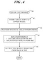
- FIG. 4 shows a flowchart of a wafer test process 80 that may be performed utilizing system 20 during, for example, wafer manufacturing.
- Wafer test process 80 provides a generalized description of the operations for implementing a contactless magnetic field programming approach to concurrently program all of IC dies 22 on wafer 24.
- wafer test process 80 combines the magnetic field programming approach for download of a test program with built-in self-test (BIST) mechanism 70 within each of IC dies 22 in order to perform wafer level testing/probing of IC dies 22 without indexing or stepping wafer test unit 26 between each of IC dies 22 on wafer 24.
- BIST built-in self-test
- wafer test process 80 touchdown of probe element(s) 46 to probe pad(s) 48 of wafer 24 is performed in order to supply source power 54 to wafer 24.
- Wafer test process 80 continues at a block 84.
- remote magnetic field programming is performed to concurrently program all of IC dies 22 on wafer 24. Magnetic field programming is discussed hereinafter in connection with FIG. 5 .
- the test program i.e., digital test program 40, is run at each of IC dies 22. Execution of digital test program 40 initiates execution of BIST mechanism 70 and enables receipt at processor 62 of test result 72.
- test result 72 e.g., PASS or FAIL
- each of IC dies 22 may be successively enabled to modulate source power 54 to produce modulated source power 74, where the specific modulation pattern indicates PASS or FAIL.
- Modulated source power 74 can be communicated from wafer 24 to wafer test unit 26.
- the PASS/FAIL state of each IC die 22 may subsequently be recorded in wafer die map 42.
- wafer level testing is complete and wafer test process 80 ends.
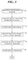
- FIG. 5 shows a flowchart of a magnetic programming process 90 executed in connection with wafer test process 80 ( FIG. 4 ). More particularly, magnetic programming process 90 is performed to concurrently program all IC dies 22 on wafer 24 at block 84 of process 80 in accordance with a particular embodiment of the invention.
- processor 34 and magnetic field transmitter 44 suitably convert digital test program 40 to magnetic signal 58, as discussed above.
- magnetic field transmitter 44 outputs magnetic signal 58.
- magnetic signal 58 may be sequence of pulses of the magnetic field (e.g., ON and OFF pulses), a sequence of magnetic field polarities (e.g., north (N) and south (S)), or any other variable magnetic field corresponding to digital test program 40.
- magnetic signal 58 is detected by (i.e., received at) each of Hall effect sensors 60 embedded in wafer 24 at a block 96.
- processors 62 in wafer 24 convert the received magnetic signal 58 to digital test program 40.
- digital test program 40 is stored in memory element 64 of each subsystem 32 on wafer 24 at a block 100 and magnetic programming process 90 ends.
- the outcome of magnetic programming process 90 is to concurrently download digital test program 40 to all IC dies 22 on wafer 24 that were identified as being "good” (i.e., not having a short circuit).
- This downloaded and stored digital test program 40 is stored for later execution in accordance with wafer test process 80 ( FIG. 4 ).
- An embodiment of a system for programming IC dies formed on a wafer comprises a magnetic field transmitter configured to output a digital program as a magnetic signal and a digital magnetic sensor formed with the IC dies of the wafer, the digital magnetic sensor being configured to receive the magnetic signal from the magnetic field transmitter.
- the system further comprises a processor formed on the wafer and in communication with digital magnetic sensor, the processor being adapted to convert the magnetic signal to the digital program, and a memory element associated with one of the IC dies on the wafer, the memory element being adapted to store the digital program.
- An embodiment of a method of programming IC dies formed on a wafer comprises transmitting a digital program as a magnetic signal from a magnetic field transmitter and receiving the magnetic signal from the magnetic field transmitter at a digital magnetic sensor formed with the IC dies of the wafer. The method further comprises converting the magnetic signal to the digital program at a processor formed on the wafer and in communication with the digital magnetic sensor, and storing the digital program in a memory element associated with one of the IC dies on the wafer.
- the systems and processes, discussed above, and the inventive principles thereof provide a remote magnetic field programming approach to concurrently program all of the IC dies on the a wafer without the need for separate communication between the test unit and each individual IC die. Accordingly, test time and cost can be dramatically reduced. Furthermore, by combining the magnetic programming approach for download of a test program with built-in self-test (BIST) functionality, wafer level testing/probing of the IC dies can be carried out without indexing or stepping the tester between each of the IC dies on the wafer in order to further reduce test time and test cost.
- BIST built-in self-test
- a method of programming integrated circuit (IC) dies formed on a wafer comprises: transmitting a digital program as a magnetic signal from a magnetic field transmitter; receiving said magnetic signal from said magnetic field transmitter at a digital magnetic sensor formed with said IC dies of said wafer; converting said magnetic signal to said digital program at a processor formed on said wafer and in communication with said magnetic field transmitter; and storing said digital program in a memory element associated with one of said IC dies on said wafer.
- IC integrated circuit
- the above method further comprises:
- a wafer test unit includes a probe card, said magnetic field transmitter and a probe element are coupled to said probe card, and the above method further comprises:
Landscapes
- Physics & Mathematics (AREA)
- Engineering & Computer Science (AREA)
- General Physics & Mathematics (AREA)
- General Engineering & Computer Science (AREA)
- Computer Hardware Design (AREA)
- Condensed Matter Physics & Semiconductors (AREA)
- Microelectronics & Electronic Packaging (AREA)
- Testing Or Measuring Of Semiconductors Or The Like (AREA)
Abstract
Description
- The present invention relates generally to integrated circuits. More specifically, the present invention relates to a system and method for magnetic field programming of integrated circuits on a wafer for wafer level testing.
- Wafer level probing and/or wafer level chip scale package (WLCSP) testing of a complimentary metal-oxide-semiconductor (CMOS) wafer containing a plurality of integrated circuit (IC) dies typically requires communication between the external test equipment (e.g., tester) and the device under test (e.g., an IC die). A primary aspect of the communication is to download a test program from the tester to each IC die on the wafer and then receive the test results to verify if the IC die under test is a good die or a bad die.
- IC dies are increasingly being fabricated with a build-in self-test (BIST) mechanism or function. A BIST function or mechanism permits an IC die to verify all or a portion of the internal functionality of the IC die. Inclusion of a BIST can reduce reliance upon and/or the complexity of external test equipment, thereby reducing test costs. For example, with the inclusion of the BIST mechanism at each IC die, a test program downloaded from the tester may simply initiate execution of the BIST, receive the test result (e.g., pass/fail) from the BIST, and communicate that result back to the tester.
- Thus, with the inclusion of a BIST mechanism, wafer level testing is becoming faster due to a reduction in communication between the tester and the devices under test. However, wafer level testing typically entails a process of die-by-die programming and testing in which a probe of the tester must index or step between each of the IC dies on the wafer. The process of indexing or stepping between each of the IC dies on the wafer to perform die-by-die programming and testing is still undesirably time consuming and costly. Therefore, a need exists in the art of wafer level testing to increase the speed of testing and thereby decrease the costs associated with testing.
- A more complete understanding of the present invention may be derived by referring to the detailed description and claims when considered in connection with the Figures, wherein like reference numbers refer to similar items throughout the Figures, the Figures are not necessarily drawn to scale, and:
-
FIG. 1 shows a block diagram of a system for programming and testing integrated circuit (IC) dies formed on or in a wafer in accordance with an embodiment; -
FIG. 2 shows a simplified top view of the wafer ofFIG. 1 ; -
FIG. 3 shows a simplified side view of a probe card of the system and a wafer under test; -
FIG. 4 shows a flowchart of a wafer test process; and -
FIG. 5 shows a flowchart of a magnetic programming process executed in connection with the wafer test process. - In overview, embodiments of the present invention entail a system and methodology for programming integrated circuit (IC) dies formed on or in a wafer. The system includes a magnetic field transmitter located at, for example, a probe card of a wafer tester and digital magnetic sensors, e.g., Hall effect sensors, formed with the IC dies on the wafer. The magnetic field transmitter outputs a test program in the form of a magnetic signal that is detectable by receiving devices, e.g., the Hall effect sensors. This magnetic signal is converted back to the test program and the test program is stored in association with each of the IC dies. By utilizing a magnetic programming approach, all of the IC dies on the wafer can be programmed concurrently without the need for communication between the tester and each individual IC die. Accordingly, test time and cost can be dramatically reduced. Furthermore, by combining the magnetic programming approach for download of a test program with built-in self-test (BIST) functionality, wafer level testing/probing of the IC dies can be carried out without indexing or stepping the tester between each of the IC dies on the wafer.
- The instant disclosure is provided to further explain in an enabling fashion the best modes, at the time of the application, of making and using various embodiments in accordance with the present invention. The disclosure is further offered to enhance an understanding and appreciation for the inventive principles and advantages thereof, rather than to limit in any manner the invention. The invention is defined solely by the appended claims including any amendments made during the pendency of this application and all equivalents of those claims as issued. It should be further understood that the use of relational terms, if any, such as first and second, top and bottom, and the like are used solely to distinguish one from another entity or action without necessarily requiring or implying any actual such relationship or order between such entities or actions.
- Referring now to
FIG. 1, FIG. 1 shows a block diagram of asystem 20 for remote programming and testing integrated circuit (IC) dies 22 formed on or in awafer 24 in accordance with an embodiment. IC dies 22 may encompass microprocessors, microcontrollers, static random access memory (RAM), and other digital logic circuits fabricated in accordance with complementary metal-oxide-semiconductor (CMOS) process technology. IC dies 22 may further encompass some analog circuits such as CMOS image sensors, data converters, radiofrequency (RF) transceivers, operational amplifiers, and the like. In accordance with CMOS process technology, the IC dies 22 ofwafer 24 use a combination of p-type and n-type metal-oxide-semiconductor field-effect-transistors (MOSFETs) to implement logic gates and other digital circuits. - For simplicity of illustration in the block diagram of
FIG. 1 ,wafer 24 is represented by a rectangle and themultiple IC dies 22 are represented by a series of three rectangles that appear to be stacked one on top of the other. It should be readily apparent to those skilled in the art that IC dies 22 are not formed in a stacked relationship on arectangular wafer 24. Rather the multiple IC dies 22 ofwafer 24 are laterally spaced from one another relative to the plane ofwafer 24. -
System 20 generally includes awafer test unit 26 having aprobe card 28, and a plurality ofsubsystems 32 formed onwafer 24.Wafer test unit 26 may be a conventional tester, sometimes referred to as a wafer prober, used to test integrated circuits.Wafer test unit 26 can include one ormore processors 34, apower source 36, and amemory element 38. In general,processor 34 may control the operation ofprobe card 28 andpower source 36. -
Processor 34 may additionally, or alternatively, enable access to and frommemory element 38. Those skilled in the art will recognize thatwafer test unit 26 can include a variety of functional elements and mechanisms for loading and unloadingwafers 24 onto a wafer chuck, pattern recognition optics for suitably aligningwafer 24 on the wafer chuck, and so forth. Details of these additional functional elements and mechanisms will not be explained in any greater extent than that considered necessary for the understanding and appreciation of the underlying concepts of the examples set forth herein and in order not to obscure or distract from the teachings herein. -
Memory element 38 may have adigital test program 40 and awafer die map 42, sometimes referred to as a wafermap, stored therein. As will be discussed in significantly greater detail below,digital test program 40 is used bysystem 20 to test IC dies 22 onwafer 24. Information regarding those IC dies 22 that are good, i.e., passing, may be stored inwafer die map 42 along with their locations onwafer 24. Wafer diemap 42 may be used to categorize the passing and non-passing IC dies 22 by making use of bins. A bin can then be identified as containing good dies or as containing bad dies. Waferdie map 42 can then be sent to subsequent die handling equipment which only picks up the passing IC dies 22 by selecting the bin number of the good IC dies 22. In other systems, non-passing IC dies 22 may be marked with a small dot of ink in the middle of the dies in lieu ofwafer die map 42. When ink dots are used, vision systems on subsequent die handling equipment can disqualify theIC dies 22 by recognizing the ink dot. -
System 20 is particularly configured to enable non-contact communication ofdigital test program 40 fromwafer test unit 26 to wafer 24. To that end, amagnetic field transmitter 44 is coupled toprobe card 28. However, IC dies 22 must be energized prior to communication ofdigital test program 40 fromwafer test unit 26 to wafer 24. Thus, at least oneprobe element 46 is additionally coupled toprobe card 28.Probe element 46 is configured for touch down on at least oneprobe pad 48 onwafer 24.Probe pad 48, in turn, may be interconnected with one or more IC dies 22 via electricallyconductive traces 52 to provide power to IC dies 22. As such,source power 54, labeled PWR, can be provided frompower source 36 to each of IC dies 22 onwafer 24 viaprobe element 46,probe pad 48 andconductive traces 52 in order to energize the circuitry of IC dies 22. - After IC dies 22 are energized, subsystems 32 (one each of which is associated with one each of IC dies 22), can be programmed and IC dies 22 may be tested. In an embodiment,
processor 34 accessesdigital test program 40 frommemory element 38 and convertsdigital test program 40 into a sequence of signals that are representative ofdigital test program 40. By way of example,digital test program 40 may be converted to its corresponding binary code, in the form of binary digits (e.g., 0's and 1's). This series of binary digits is referred to herein as binary code 56, and is labeled PB inFIG. 1 . Binary code 56 can be communicated fromwafer test unit 36 tomagnetic field transmitter 44.Magnetic field transmitter 44 does not physically contact IC dies 22 ofwafer 24. Instead,magnetic field transmitter 44 can include one or more magnetic coil structures that generate and output a magnetic field, referred to herein as amagnetic signal 58, labeled SMAG, corresponding to binary code 56.Magnetic signal 58 is emitted frommagnetic field transmitter 44 over a relatively short distance as a change in the magnetic field aroundmagnetic field transmitter 44. Whenmagnetic field transmitter 44 includes more than one magnetic coil structure,magnetic signal 58 may be output from the multiple magnetic coil structures, in a serial or parallel manner, to collectively flood theentire wafer 24. - Accordingly,
magnetic signal 58 is represented by a series of dashed lines to indicate its communication towafer 24 via non-physical contact. Again by way of example, the output magnetic field (i.e., magnetic signal 58) may include two magnitudes, where one magnitude corresponds to a "0" in binary code 56 and another magnitude corresponds to a "1" in binary code 56. In an example embodiment,magnetic field transmitter 44 can modulate binary code 56 as a sequence of pulses of the magnetic field (e.g., ON and OFF pulses) or a sequence of magnetic field polarities (e.g., north (N) and south (S)) to generatemagnetic signal 58. It should be understood however, thatdigital test program 40 may be converted into any suitable code that is thereafter output frommagnetic field transmitter 44 asmagnetic signal 58. - Each of
subsystems 32 includes a digitalmagnetic sensor 60 formed with its associated IC die 22, aprocessor 62 in communication with digitalmagnetic sensor 60, and a memory element 64 in communication withprocessor 62. Digitalmagnetic sensor 60 is adapted to detect and receivemagnetic signal 58. In operation, digitalmagnetic sensor 60 can sense, for example, the sequence of pulses of the magnetic field (e.g., ON and OFF pulses) or the sequence of magnetic field polarities (e.g., north (N) and south (S)) ofmagnetic signal 58. Digitalmagnetic sensor 60 may be, for example, a Hall effect sensor that varies its output voltage in response to a magnetic field, e.g.,magnetic signal 58. As such, digitalmagnetic sensor 60 is referred to hereinafter asHall effect sensor 60.
Hall effect sensor 60 can be a single crystal silicon-based sensor that does not include magnetic materials. As such,Hall effect sensor 60 can be readily fabricated in accordance with the process flow for constructing IC dies 22. Furthermore,magnetic signal 58 can readily penetrate insidewafer 24. Therefore,Hall effect sensor 60 need not be fabricated on the surface ofwafer 24, but may instead be embedded within and under the surface ofwafer 24. -
Hall effect sensor 60 can decode the sensedmagnetic signal 58 and communicatemagnetic signal 58 as anoutput voltage 66, labeled Vo, toprocessor 62. In an embodiment,output voltage 66 corresponds with binary code 56. As such,processor 62 can convert or otherwise determinedigital test program 40 fromoutput voltage 66. Accordingly,processor 62, in cooperation withHall effect sensor 60, is adapted to convertmagnetic signal 58 todigital test program 40. Thereafter,processor 62 communicatesdigital test program 40 to memory element 64, wheredigital test program 40 is stored. - In accordance with a particular embodiment,
magnetic field transmitter 44 is configured to flood an entire surface ofwafer 24 withmagnetic signal 58. Thus, each ofsubsystems 32 concurrently receivesmagnetic signal 58, convertsmagnetic signal 58 todigital test program 40, and storesdigital test program 40 in memory element 64 of its corresponding IC die 22. Consequently,digital test program 40 can be loaded to all of IC dies 22 onwafer 24 in parallel via a remote magnetic field programming approach withHall effect sensors 60 being the receiving elements without the need for physical communication fromwafer test unit 26 on a die-by-die basis to each individual IC die 22. - Each of IC dies 22 includes
functional circuitry 68. Additionally, each of IC dies 22 may include a built-in self-test (BIST)mechanism 70, or BIST processor.BIST mechanism 70 permits each of IC dies 22 to test itself in order to determine the functionality of its associated IC die. By way of example,BIST mechanism 70 functions to verify all or a portion of the internal functionality of its corresponding IC die 22 and produce atest result 72 of that functionality. Thus,BIST mechanism 70 can be implemented to perform faster, less-expensive integrated circuit testing. - In a wafer level testing scenario,
processor 62 functions as a BIST controller anddigital test program 40 includes a minimal set of instructions for initiating execution ofBIST mechanism 70, receiving and storingtest result 72 in memory element 64, and thereafter communicatingtest result 72 towafer test unit 26. In an embodiment discussed below,processor 62 may modulatesource power 54 in accordance withtest result 72 to produce modulatedsource power 74, labeled PWR(MOD).Modulated source power 74 containingtest result 72 can then be returned towafer test unit 26 viaprobe element 46. In one example,test result 72 may be a simple PASS or FAIL result. In an embodiment, modulatedsource power 74 may be produced by modulating the voltage ofsource power 54 provided to IC dies 22. For example, the voltage may be modulated to produce one voltage magnitude for a PASS result and a different voltage magnitude for a FAIL result. In another embodiment,processor 62 may modulate the current ofsource power 54 in accordance withtest result 72 to produce a modulatedsource power 74. By way of example, the current may be modulated to produce higher current (e.g., higher power) for a PASS result and a lower current (e.g., lower power) for a FAIL result.Modulated source power 74 containingtest result 72 can then be return towafer test unit 26 viaprobe element 46. - Accordingly, execution of each
digital test program 40, loaded to all of IC dies 22 onwafer 24 in parallel via a remote magnetic field programming approach, controls operation ofBIST mechanism 70 on each IC die 22. Therefore, all IC dies 22 onwafer 24 can be tested and probed without the need forwafer test unit 26 to program each IC die 22 withdigital test program 40 individually in series, without executingBIST mechanism 70 of each IC die 22 individually in series, and without requiring physical die-by-die indexing ofprobe element 46 to receivetest result 72. Thus, each of IC dies 22 may be tested in parallel which can significantly reduce test time for anentire wafer 24 and therefore significantly reduce test costs. -
FIG. 2 shows a simplified top view ofwafer 24 ofFIG. 1 on or in which IC dies 22 are formed. Each of IC dies 22 can includefunctional circuitry 68,BIST mechanism 70, andsubsystem 32. Additionally,wafer 24 can includeprobe pad 48 located in an unused portion ofwafer 24, such as at an outer periphery ofwafer 24. Conductive traces 52, as well as other unspecified interconnections, are not shown for simplicity.Wafer 24 includes only a few IC dies 22 for simplicity of illustration. Those skilled in the art will recognize that a single wafer can include hundreds, thousands, or even tens of thousands of individual IC dies 22. - IC dies 22 are separated by
scribe lines 76 formed in asurface 78 ofwafer 24. A first set ofscribe lines 76 may extend parallel to one another in one direction, i.e., horizontally across asurface 78 ofwafer 24. Another set ofscribe lines 76 may extend substantially parallel to one another acrosssurface 78 ofwafer 24 in a different direction or substantially orthogonal to the first set of scribe lines 76. Scribe lines 76 may form substantially square or rectangular areas, each of which define IC die 22 or semiconductor chip. Scribe lines 76 can be used to separate each of IC dies 22 after fabrication. In an example, eachsubsystem 32 is located within an area circumscribed byscribe lines 76. However,scribe lines 76 may have a predetermined width that permitssubsystems 32 and/or conductive traces 52 (shown inFIG. 1 ) to be located within scribe lines 76. Thus, IC dies 22 may be tested at wafer level, i.e., prior to dicing, during the manufacturing process. - Each
subsystem 32 is located within an area circumscribed byscribe lines 76 to emphasize that each IC die 22 may have aHall effect sensor 60,processor 62, and memory element 64 (FIG. 1 ) associated with it. It should be understood that various alternative subsystem configurations may be envisioned. For example, oneHall effect sensor 60 may be associated with more than one IC die 22 but less than all of the IC dies 22 onwafer 24 and communicate its output via conductive lines (not shown) to a plurality subsystems associated with the subset of IC dies 22, where each of the subsystems includes one ofprocessors 62 and memory elements 64. Furthermore, asingle probe pad 48 is shown for simplicity of illustration. However,wafer 24 can includemultiple probe pads 48, each of which can communicate source power 54 (FIG. 1 ) to a subset of IC dies 22. -
FIG. 3 shows a simplified side view ofprobe card 28 of system 20 (FIG. 1 ) andwafer 24 under test. More particularly,probe card 28 is shown withmagnetic field transmitter 44, e.g., one or more coils, for outputtingmagnetic signal 58, and twoprobe elements 46.Wafer 24 is shown with a number of IC dies 22 formed therein, where each IC die 22 includes functional circuitry 68 (FIG. 1 ), BIST mechanism 70 (FIG. 1 ), and one of subsystems 32 (FIG. 1 ) that includes Hall effect sensor 60 (FIG. 1 ) for receivingmagnetic signal 58. - Probe
elements 46 may touch down ontoprobe pads 48 formed onwafer 24 to provide source power 54 (FIG. 1 ). However,magnetic field transmitter 44 does not physically contact IC dies 22 orwafer 24. Rather,magnetic field transmitter 44 floods theentire surface 78 ofwafer 24 withmagnetic signal 58 to enable parallel programming of all of IC dies 22 onwafer 24 via a remote magnetic field programming approach. - Now referring to
FIG. 4 in conjunction withFIG. 1 ,FIG. 4 shows a flowchart of awafer test process 80 that may be performed utilizingsystem 20 during, for example, wafer manufacturing.Wafer test process 80 provides a generalized description of the operations for implementing a contactless magnetic field programming approach to concurrently program all of IC dies 22 onwafer 24. Furthermore,wafer test process 80 combines the magnetic field programming approach for download of a test program with built-in self-test (BIST)mechanism 70 within each of IC dies 22 in order to perform wafer level testing/probing of IC dies 22 without indexing or steppingwafer test unit 26 between each of IC dies 22 onwafer 24. - At a
block 82 ofwafer test process 80, touchdown of probe element(s) 46 to probe pad(s) 48 ofwafer 24 is performed in order to supplysource power 54 towafer 24.Wafer test process 80 continues at ablock 84. Atblock 84, remote magnetic field programming is performed to concurrently program all of IC dies 22 onwafer 24. Magnetic field programming is discussed hereinafter in connection withFIG. 5 . At ablock 86, the test program, i.e.,digital test program 40, is run at each of IC dies 22. Execution ofdigital test program 40 initiates execution ofBIST mechanism 70 and enables receipt atprocessor 62 oftest result 72. - At a
block 88,test result 72, e.g., PASS or FAIL, for each IC die 22 is output from its associatedsubsystem 32. In one example, each of IC dies 22 may be successively enabled to modulatesource power 54 to produce modulatedsource power 74, where the specific modulation pattern indicates PASS or FAIL.Modulated source power 74 can be communicated fromwafer 24 towafer test unit 26. The PASS/FAIL state of each IC die 22 may subsequently be recorded in wafer diemap 42. Followingblock 88, wafer level testing is complete andwafer test process 80 ends.
Referring now toFIGs. 1 and5, FIG. 5 shows a flowchart of amagnetic programming process 90 executed in connection with wafer test process 80 (FIG. 4 ). More particularly,magnetic programming process 90 is performed to concurrently program all IC dies 22 onwafer 24 atblock 84 ofprocess 80 in accordance with a particular embodiment of the invention. - At a
block 92 ofmagnetic programming process 90,processor 34 andmagnetic field transmitter 44 suitably convertdigital test program 40 tomagnetic signal 58, as discussed above. At ablock 94,magnetic field transmitter 44 outputsmagnetic signal 58. Again,magnetic signal 58 may be sequence of pulses of the magnetic field (e.g., ON and OFF pulses), a sequence of magnetic field polarities (e.g., north (N) and south (S)), or any other variable magnetic field corresponding todigital test program 40.
In response to the transmission ofmagnetic signal 58 atblock 94,magnetic signal 58 is detected by (i.e., received at) each ofHall effect sensors 60 embedded inwafer 24 at ablock 96. At ablock 98,processors 62 inwafer 24 convert the receivedmagnetic signal 58 todigital test program 40. Thereafter,digital test program 40 is stored in memory element 64 of eachsubsystem 32 onwafer 24 at ablock 100 andmagnetic programming process 90 ends. Thus, the outcome ofmagnetic programming process 90 is to concurrently downloaddigital test program 40 to all IC dies 22 onwafer 24 that were identified as being "good" (i.e., not having a short circuit). This downloaded and storeddigital test program 40 is stored for later execution in accordance with wafer test process 80 (FIG. 4 ). - It is to be understood that certain ones of the process blocks depicted in
FIGs. 4 and5 may be performed in parallel with each other or with performing other processes. In addition, it is to be understood that the particular ordering of the process blocks depicted inFIGs. 4 and5 may be modified, while achieving substantially the same result. Accordingly, such modifications are intended to be included within the scope of the inventive subject matter. - Thus, a system and a method for programming IC dies formed on a wafer have been described. An embodiment of a system for programming IC dies formed on a wafer comprises a magnetic field transmitter configured to output a digital program as a magnetic signal and a digital magnetic sensor formed with the IC dies of the wafer, the digital magnetic sensor being configured to receive the magnetic signal from the magnetic field transmitter. The system further comprises a processor formed on the wafer and in communication with digital magnetic sensor, the processor being adapted to convert the magnetic signal to the digital program, and a memory element associated with one of the IC dies on the wafer, the memory element being adapted to store the digital program.
- An embodiment of a method of programming IC dies formed on a wafer comprises transmitting a digital program as a magnetic signal from a magnetic field transmitter and receiving the magnetic signal from the magnetic field transmitter at a digital magnetic sensor formed with the IC dies of the wafer. The method further comprises converting the magnetic signal to the digital program at a processor formed on the wafer and in communication with the digital magnetic sensor, and storing the digital program in a memory element associated with one of the IC dies on the wafer.
- The systems and processes, discussed above, and the inventive principles thereof provide a remote magnetic field programming approach to concurrently program all of the IC dies on the a wafer without the need for separate communication between the test unit and each individual IC die. Accordingly, test time and cost can be dramatically reduced. Furthermore, by combining the magnetic programming approach for download of a test program with built-in self-test (BIST) functionality, wafer level testing/probing of the IC dies can be carried out without indexing or stepping the tester between each of the IC dies on the wafer in order to further reduce test time and test cost.
- In particular, in one example of the present application a method of programming integrated circuit (IC) dies formed on a wafer is provided, which comprises: transmitting a digital program as a magnetic signal from a magnetic field transmitter; receiving said magnetic signal from said magnetic field transmitter at a digital magnetic sensor formed with said IC dies of said wafer;
converting said magnetic signal to said digital program at a processor formed on said wafer and in communication with said magnetic field transmitter; and storing said digital program in a memory element associated with one of said IC dies on said wafer. - In a further example, the above method further comprises:
- fabricating said wafer to include a plurality of subsystems, one each of said subsystems being formed with one each of said IC dies of said wafer, each of said subsystems comprising said digital magnetic sensor, said processor in communication with said digital magnetic sensor, and said memory element in communication with said processor; and
- flooding an entire surface of said wafer with said magnetic signal such that each of said subsystems concurrently receives said magnetic signal, converts said magnetic signal to said digital program, and stores said digital program in association with said one each of said IC dies.
- In a further example, a wafer test unit includes a probe card, said magnetic field transmitter and a probe element are coupled to said probe card, and the above method further comprises:
- fabricating a probe pad on said wafer that is electrically coupled with said IC dies;
- touching said probe element on said probe pad to selectively provide source power to each of said IC dies; and
- following provision of said source power, performing said transmitting operation without said magnetic field transmitter element contacting said IC dies.
- This disclosure is intended to explain how to fashion and use various embodiments in accordance with the invention rather than to limit the true, intended, and fair scope and spirit thereof. The foregoing description is not intended to be exhaustive or to limit the invention to the precise form disclosed. Modifications or variations are possible in light of the above teachings. The embodiment(s) was chosen and described to provide the best illustration of the principles of the invention and its practical application, and to enable one of ordinary skill in the art to utilize the invention in various embodiments and with various modifications as are suited to the particular use contemplated. All such modifications and variations are within the scope of the invention as determined by the appended claims, as may be amended during the pendency of this application for patent, and all equivalents thereof, when interpreted in accordance with the breadth to which they are fairly, legally, and equitably entitled.
Claims (15)
- A system for programming integrated circuit (IC) dies formed on a wafer comprising:a magnetic field transmitter configured to output a digital program as a magnetic signal;a digital magnetic sensor formed with said IC dies of said wafer, said digital magnetic sensor being configured to receive said magnetic signal from said magnetic field transmitter;a processor formed on said wafer and in communication with said digital magnetic sensor, said processor being adapted to convert said magnetic signal to said digital program; anda memory element associated with one of said IC dies on said wafer, said memory element being adapted to store said digital program, wherein said magnetic field transmitter is adapted to modulate said digital program as a sequence of pulses of a magnetic field, said sequence of pulses forming said magnetic signal.
- The system of claim 1, wherein said magnetic field transmitter does not physically contact said IC dies.
- The system of claims 1 or 2, wherein said magnetic field transmitter is adapted to modulate said digital program as a sequence of pulses of a magnetic field, said sequence of pulses forming said magnetic signal.
- The system of anyone of the preceding claims, wherein said digital magnetic sensor comprises a Hall effect sensor.
- The system of anyone of the preceding claims, wherein said digital magnetic sensor is embedded within said wafer.
- The system of anyone of the preceding claims, wherein digital magnetic sensor is one of a plurality of digital magnetic sensors, one each of said digital magnetic sensors being formed with one each of said IC dies of said wafer.
- The system of anyone of the preceding claims, wherein said processor is one of a plurality of processors, one each of said processors being formed with one each of said IC dies of said wafer, and said each of said processors is adapted to receive and convert said magnetic signal to said digital program.
- The system of anyone of the preceding claims, wherein said memory element is one of a plurality of memory elements, one each of said memory elements being formed with one each of said IC dies of said wafer, and said each of said memory elements is adapted to store said digital program.
- The system of anyone of the preceding claims, wherein said one of said IC dies includes a built-in self-test (BIST) mechanism to determine a functionality of said one of said IC dies, and said processor is configured to communicate with said BIST mechanism, wherein execution of said digital program initiates operation of said BIST mechanism and receipt of a test result from said BIST mechanism.
- The system of anyone of the preceding claims, further comprising:a wafer test unit having a probe card, said magnetic field transmitter and a probe element being coupled to said probe card, wherein said probe element provides source power; anda probe pad on said wafer and electrically coupled with said IC dies, said probe element being configured for touchdown on said probe pad to selectively provide said source power to each of said IC dies.
- The system of claim 10, wherein said processor is further configured to execute said digital program, receive a test result indicative of a functionality of said one of said IC dies, and modulate said source power in accordance with said test result to return said test result to said wafer test unit.
- A system for programming integrated circuit (IC) dies formed on a wafer comprising:a magnetic field transmitter configured to output a digital program as a magnetic signal;a plurality of subsystems, one each of said subsystems being formed with one each of said IC dies of said wafer, each of said subsystems comprising:a digital magnetic sensor for receiving said magnetic signal from said magnetic field transmitter;a processor in communication with said digital magnetic sensor for converting said magnetic signal to said digital program; anda memory element in communication with said processor for storing said digital program, wherein said magnetic field transmitter is configured to flood an entire surface of said wafer with said magnetic signal such that each of said subsystems concurrently receives said magnetic signal, converts said magnetic signal to said digital program, and stores said digital program.
- The system of claim 12, wherein said magnetic field transmitter does not physically contact said IC dies.
- The system of claims 12 or 13, further comprising:a wafer test unit having a probe card, said magnetic field transmitter and a probe element being coupled to said probe card, wherein said probe element provides source power; anda probe pad on said wafer and electrically coupled with said IC dies, said probe element being configured for touchdown on said probe pad to selectively provide said source power to each of said IC dies.
- The system of claim 14, wherein each of said IC dies includes a built-in self-test (BIST) mechanism to determine a functionality of said each of said IC dies, said processor is configured to communicate with said BIST mechanism and execute said digital program, wherein execution of said digital program initiates operation of said BIST mechanism and receipt of a test result from said BIST mechanism, said test result being indicative of said functionality of said one of said IC dies, and said processor is further configured to modulate said source power in accordance with said test result to return said test result to said wafer test unit.
Priority Applications (1)
| Application Number | Priority Date | Filing Date | Title |
|---|---|---|---|
| EP16160536.5A EP3070486B1 (en) | 2015-03-16 | 2016-03-15 | Magnetic field programming of electronic devices on a wafer |
Applications Claiming Priority (2)
| Application Number | Priority Date | Filing Date | Title |
|---|---|---|---|
| IB2015000515 | 2015-03-16 | ||
| EP16160536.5A EP3070486B1 (en) | 2015-03-16 | 2016-03-15 | Magnetic field programming of electronic devices on a wafer |
Publications (2)
| Publication Number | Publication Date |
|---|---|
| EP3070486A1 true EP3070486A1 (en) | 2016-09-21 |
| EP3070486B1 EP3070486B1 (en) | 2019-01-02 |
Family
ID=64565019
Family Applications (1)
| Application Number | Title | Priority Date | Filing Date |
|---|---|---|---|
| EP16160536.5A Not-in-force EP3070486B1 (en) | 2015-03-16 | 2016-03-15 | Magnetic field programming of electronic devices on a wafer |
Country Status (1)
| Country | Link |
|---|---|
| EP (1) | EP3070486B1 (en) |
Cited By (1)
| Publication number | Priority date | Publication date | Assignee | Title |
|---|---|---|---|---|
| CN113748350A (en) * | 2020-02-10 | 2021-12-03 | 株式会社爱德万测试 | Testing device |
Citations (3)
| Publication number | Priority date | Publication date | Assignee | Title |
|---|---|---|---|---|
| US20020196029A1 (en) * | 2001-06-22 | 2002-12-26 | Schmidt Dominik J. | Systems and methods for testing wireless devices |
| US20050138499A1 (en) * | 2003-11-26 | 2005-06-23 | Lawrence Pileggi | System and method to test integrated circuits on a wafer |
| US20130021048A1 (en) * | 2011-06-13 | 2013-01-24 | Media Tek Inc. | Ic, circuitry, and rf bist system |
Family Cites Families (1)
| Publication number | Priority date | Publication date | Assignee | Title |
|---|---|---|---|---|
| US20090218657A1 (en) * | 2008-03-03 | 2009-09-03 | Broadcom Corporation | Inductively coupled integrated circuit with near field communication and methods for use therewith |
-
2016
- 2016-03-15 EP EP16160536.5A patent/EP3070486B1/en not_active Not-in-force
Patent Citations (4)
| Publication number | Priority date | Publication date | Assignee | Title |
|---|---|---|---|---|
| US20020196029A1 (en) * | 2001-06-22 | 2002-12-26 | Schmidt Dominik J. | Systems and methods for testing wireless devices |
| US7057518B2 (en) * | 2001-06-22 | 2006-06-06 | Schmidt Dominik J | Systems and methods for testing wireless devices |
| US20050138499A1 (en) * | 2003-11-26 | 2005-06-23 | Lawrence Pileggi | System and method to test integrated circuits on a wafer |
| US20130021048A1 (en) * | 2011-06-13 | 2013-01-24 | Media Tek Inc. | Ic, circuitry, and rf bist system |
Cited By (2)
| Publication number | Priority date | Publication date | Assignee | Title |
|---|---|---|---|---|
| CN113748350A (en) * | 2020-02-10 | 2021-12-03 | 株式会社爱德万测试 | Testing device |
| US12241926B2 (en) | 2020-02-10 | 2025-03-04 | Advantest Corporation | Test apparatus |
Also Published As
| Publication number | Publication date |
|---|---|
| EP3070486B1 (en) | 2019-01-02 |
Similar Documents
| Publication | Publication Date | Title |
|---|---|---|
| US9607911B2 (en) | Optical programming of electronic devices on a wafer | |
| US10651147B2 (en) | Signal isolator having bidirectional communication between die | |
| US8826086B2 (en) | Memory card test interface | |
| US5764655A (en) | Built in self test with memory | |
| US9891267B2 (en) | Kernel based cluster fault analysis | |
| US9824774B2 (en) | Magnetic field programming of electronic devices on a wafer | |
| US9784787B2 (en) | Electric field sensor, system, and method for programming electronic devices on a wafer | |
| CN109037090B (en) | Multiple test type probe cards and corresponding test systems | |
| CN104076194B (en) | Test the output short circuit current of ic package | |
| CN114388043B (en) | Target test not passing injection | |
| CN104237577B (en) | The method and apparatus of wafer sort | |
| CN104062534A (en) | Testing Integrated Circuit Packaging For Shorts | |
| US9536118B2 (en) | Card reader and method of operating the same | |
| JP2015001761A (en) | Authentication device, authentication method, and program | |
| US10739401B2 (en) | Logic built in self test circuitry for use in an integrated circuit with scan chains | |
| US20140032985A1 (en) | Scan test circuitry configured to prevent capture of potentially non-deterministic values | |
| EP3070486B1 (en) | Magnetic field programming of electronic devices on a wafer | |
| WO2012128760A1 (en) | System and method for electronic testing of partially processed devices | |
| US20080116910A1 (en) | Apparatus for mass die testing | |
| US20160274188A1 (en) | Wafer-level magnetic field programming of magnetic field sensors | |
| US20160320445A1 (en) | Probeless parallel test system and method for integrated circuit | |
| WO2015119541A1 (en) | Configurable built-in self-tests of digital logic circuits | |
| US20140365838A1 (en) | Integrated circuit comprising test circuitry for testing fan-out paths of a test control primary input | |
| US20160187380A1 (en) | Method and Apparatus for RFID Tag Testing | |
| CN100516914C (en) | Integrated circuit and corresponding packaged integrated circuit |
Legal Events
| Date | Code | Title | Description |
|---|---|---|---|
| PUAI | Public reference made under article 153(3) epc to a published international application that has entered the european phase |
Free format text: ORIGINAL CODE: 0009012 |
|
| AK | Designated contracting states |
Kind code of ref document: A1 Designated state(s): AL AT BE BG CH CY CZ DE DK EE ES FI FR GB GR HR HU IE IS IT LI LT LU LV MC MK MT NL NO PL PT RO RS SE SI SK SM TR |
|
| AX | Request for extension of the european patent |
Extension state: BA ME |
|
| RAP1 | Party data changed (applicant data changed or rights of an application transferred) |
Owner name: NXP USA, INC. |
|
| STAA | Information on the status of an ep patent application or granted ep patent |
Free format text: STATUS: REQUEST FOR EXAMINATION WAS MADE |
|
| 17P | Request for examination filed |
Effective date: 20170321 |
|
| RBV | Designated contracting states (corrected) |
Designated state(s): AL AT BE BG CH CY CZ DE DK EE ES FI FR GB GR HR HU IE IS IT LI LT LU LV MC MK MT NL NO PL PT RO RS SE SI SK SM TR |
|
| STAA | Information on the status of an ep patent application or granted ep patent |
Free format text: STATUS: EXAMINATION IS IN PROGRESS |
|
| 17Q | First examination report despatched |
Effective date: 20171011 |
|
| GRAP | Despatch of communication of intention to grant a patent |
Free format text: ORIGINAL CODE: EPIDOSNIGR1 |
|
| STAA | Information on the status of an ep patent application or granted ep patent |
Free format text: STATUS: GRANT OF PATENT IS INTENDED |
|
| RIC1 | Information provided on ipc code assigned before grant |
Ipc: G11C 11/18 20060101ALI20180911BHEP Ipc: G11C 29/12 20060101ALI20180911BHEP Ipc: G01R 31/319 20060101ALI20180911BHEP Ipc: G01R 31/28 20060101AFI20180911BHEP Ipc: G01R 31/317 20060101ALI20180911BHEP Ipc: G01R 33/07 20060101ALI20180911BHEP Ipc: G01R 31/3187 20060101ALI20180911BHEP |
|
| INTG | Intention to grant announced |
Effective date: 20181010 |
|
| GRAS | Grant fee paid |
Free format text: ORIGINAL CODE: EPIDOSNIGR3 |
|
| GRAA | (expected) grant |
Free format text: ORIGINAL CODE: 0009210 |
|
| STAA | Information on the status of an ep patent application or granted ep patent |
Free format text: STATUS: THE PATENT HAS BEEN GRANTED |
|
| AK | Designated contracting states |
Kind code of ref document: B1 Designated state(s): AL AT BE BG CH CY CZ DE DK EE ES FI FR GB GR HR HU IE IS IT LI LT LU LV MC MK MT NL NO PL PT RO RS SE SI SK SM TR |
|
| REG | Reference to a national code |
Ref country code: GB Ref legal event code: FG4D |
|
| REG | Reference to a national code |
Ref country code: CH Ref legal event code: EP Ref country code: AT Ref legal event code: REF Ref document number: 1085086 Country of ref document: AT Kind code of ref document: T Effective date: 20190115 |
|
| REG | Reference to a national code |
Ref country code: IE Ref legal event code: FG4D |
|
| REG | Reference to a national code |
Ref country code: DE Ref legal event code: R096 Ref document number: 602016008839 Country of ref document: DE |
|
| REG | Reference to a national code |
Ref country code: NL Ref legal event code: MP Effective date: 20190102 |
|
| REG | Reference to a national code |
Ref country code: LT Ref legal event code: MG4D |
|
| REG | Reference to a national code |
Ref country code: AT Ref legal event code: MK05 Ref document number: 1085086 Country of ref document: AT Kind code of ref document: T Effective date: 20190102 |
|
| PG25 | Lapsed in a contracting state [announced via postgrant information from national office to epo] |
Ref country code: NL Free format text: LAPSE BECAUSE OF FAILURE TO SUBMIT A TRANSLATION OF THE DESCRIPTION OR TO PAY THE FEE WITHIN THE PRESCRIBED TIME-LIMIT Effective date: 20190102 |
|
| PG25 | Lapsed in a contracting state [announced via postgrant information from national office to epo] |
Ref country code: ES Free format text: LAPSE BECAUSE OF FAILURE TO SUBMIT A TRANSLATION OF THE DESCRIPTION OR TO PAY THE FEE WITHIN THE PRESCRIBED TIME-LIMIT Effective date: 20190102 Ref country code: LT Free format text: LAPSE BECAUSE OF FAILURE TO SUBMIT A TRANSLATION OF THE DESCRIPTION OR TO PAY THE FEE WITHIN THE PRESCRIBED TIME-LIMIT Effective date: 20190102 Ref country code: FI Free format text: LAPSE BECAUSE OF FAILURE TO SUBMIT A TRANSLATION OF THE DESCRIPTION OR TO PAY THE FEE WITHIN THE PRESCRIBED TIME-LIMIT Effective date: 20190102 Ref country code: PL Free format text: LAPSE BECAUSE OF FAILURE TO SUBMIT A TRANSLATION OF THE DESCRIPTION OR TO PAY THE FEE WITHIN THE PRESCRIBED TIME-LIMIT Effective date: 20190102 Ref country code: NO Free format text: LAPSE BECAUSE OF FAILURE TO SUBMIT A TRANSLATION OF THE DESCRIPTION OR TO PAY THE FEE WITHIN THE PRESCRIBED TIME-LIMIT Effective date: 20190402 Ref country code: PT Free format text: LAPSE BECAUSE OF FAILURE TO SUBMIT A TRANSLATION OF THE DESCRIPTION OR TO PAY THE FEE WITHIN THE PRESCRIBED TIME-LIMIT Effective date: 20190502 Ref country code: SE Free format text: LAPSE BECAUSE OF FAILURE TO SUBMIT A TRANSLATION OF THE DESCRIPTION OR TO PAY THE FEE WITHIN THE PRESCRIBED TIME-LIMIT Effective date: 20190102 |
|
| PG25 | Lapsed in a contracting state [announced via postgrant information from national office to epo] |
Ref country code: IS Free format text: LAPSE BECAUSE OF FAILURE TO SUBMIT A TRANSLATION OF THE DESCRIPTION OR TO PAY THE FEE WITHIN THE PRESCRIBED TIME-LIMIT Effective date: 20190502 Ref country code: BG Free format text: LAPSE BECAUSE OF FAILURE TO SUBMIT A TRANSLATION OF THE DESCRIPTION OR TO PAY THE FEE WITHIN THE PRESCRIBED TIME-LIMIT Effective date: 20190402 Ref country code: GR Free format text: LAPSE BECAUSE OF FAILURE TO SUBMIT A TRANSLATION OF THE DESCRIPTION OR TO PAY THE FEE WITHIN THE PRESCRIBED TIME-LIMIT Effective date: 20190403 Ref country code: RS Free format text: LAPSE BECAUSE OF FAILURE TO SUBMIT A TRANSLATION OF THE DESCRIPTION OR TO PAY THE FEE WITHIN THE PRESCRIBED TIME-LIMIT Effective date: 20190102 Ref country code: LV Free format text: LAPSE BECAUSE OF FAILURE TO SUBMIT A TRANSLATION OF THE DESCRIPTION OR TO PAY THE FEE WITHIN THE PRESCRIBED TIME-LIMIT Effective date: 20190102 Ref country code: HR Free format text: LAPSE BECAUSE OF FAILURE TO SUBMIT A TRANSLATION OF THE DESCRIPTION OR TO PAY THE FEE WITHIN THE PRESCRIBED TIME-LIMIT Effective date: 20190102 |
|
| REG | Reference to a national code |
Ref country code: DE Ref legal event code: R097 Ref document number: 602016008839 Country of ref document: DE |
|
| PG25 | Lapsed in a contracting state [announced via postgrant information from national office to epo] |
Ref country code: CZ Free format text: LAPSE BECAUSE OF FAILURE TO SUBMIT A TRANSLATION OF THE DESCRIPTION OR TO PAY THE FEE WITHIN THE PRESCRIBED TIME-LIMIT Effective date: 20190102 Ref country code: SK Free format text: LAPSE BECAUSE OF FAILURE TO SUBMIT A TRANSLATION OF THE DESCRIPTION OR TO PAY THE FEE WITHIN THE PRESCRIBED TIME-LIMIT Effective date: 20190102 Ref country code: RO Free format text: LAPSE BECAUSE OF FAILURE TO SUBMIT A TRANSLATION OF THE DESCRIPTION OR TO PAY THE FEE WITHIN THE PRESCRIBED TIME-LIMIT Effective date: 20190102 Ref country code: AL Free format text: LAPSE BECAUSE OF FAILURE TO SUBMIT A TRANSLATION OF THE DESCRIPTION OR TO PAY THE FEE WITHIN THE PRESCRIBED TIME-LIMIT Effective date: 20190102 Ref country code: MC Free format text: LAPSE BECAUSE OF FAILURE TO SUBMIT A TRANSLATION OF THE DESCRIPTION OR TO PAY THE FEE WITHIN THE PRESCRIBED TIME-LIMIT Effective date: 20190102 Ref country code: DK Free format text: LAPSE BECAUSE OF FAILURE TO SUBMIT A TRANSLATION OF THE DESCRIPTION OR TO PAY THE FEE WITHIN THE PRESCRIBED TIME-LIMIT Effective date: 20190102 Ref country code: AT Free format text: LAPSE BECAUSE OF FAILURE TO SUBMIT A TRANSLATION OF THE DESCRIPTION OR TO PAY THE FEE WITHIN THE PRESCRIBED TIME-LIMIT Effective date: 20190102 Ref country code: EE Free format text: LAPSE BECAUSE OF FAILURE TO SUBMIT A TRANSLATION OF THE DESCRIPTION OR TO PAY THE FEE WITHIN THE PRESCRIBED TIME-LIMIT Effective date: 20190102 Ref country code: IT Free format text: LAPSE BECAUSE OF FAILURE TO SUBMIT A TRANSLATION OF THE DESCRIPTION OR TO PAY THE FEE WITHIN THE PRESCRIBED TIME-LIMIT Effective date: 20190102 |
|
| REG | Reference to a national code |
Ref country code: CH Ref legal event code: PL |
|
| PLBE | No opposition filed within time limit |
Free format text: ORIGINAL CODE: 0009261 |
|
| STAA | Information on the status of an ep patent application or granted ep patent |
Free format text: STATUS: NO OPPOSITION FILED WITHIN TIME LIMIT |
|
| PG25 | Lapsed in a contracting state [announced via postgrant information from national office to epo] |
Ref country code: LU Free format text: LAPSE BECAUSE OF NON-PAYMENT OF DUE FEES Effective date: 20190315 Ref country code: SM Free format text: LAPSE BECAUSE OF FAILURE TO SUBMIT A TRANSLATION OF THE DESCRIPTION OR TO PAY THE FEE WITHIN THE PRESCRIBED TIME-LIMIT Effective date: 20190102 |
|
| 26N | No opposition filed |
Effective date: 20191003 |
|
| REG | Reference to a national code |
Ref country code: BE Ref legal event code: MM Effective date: 20190331 |
|
| PG25 | Lapsed in a contracting state [announced via postgrant information from national office to epo] |
Ref country code: IE Free format text: LAPSE BECAUSE OF NON-PAYMENT OF DUE FEES Effective date: 20190315 Ref country code: CH Free format text: LAPSE BECAUSE OF NON-PAYMENT OF DUE FEES Effective date: 20190331 Ref country code: LI Free format text: LAPSE BECAUSE OF NON-PAYMENT OF DUE FEES Effective date: 20190331 |
|
| PG25 | Lapsed in a contracting state [announced via postgrant information from national office to epo] |
Ref country code: SI Free format text: LAPSE BECAUSE OF FAILURE TO SUBMIT A TRANSLATION OF THE DESCRIPTION OR TO PAY THE FEE WITHIN THE PRESCRIBED TIME-LIMIT Effective date: 20190102 Ref country code: FR Free format text: LAPSE BECAUSE OF NON-PAYMENT OF DUE FEES Effective date: 20190331 Ref country code: BE Free format text: LAPSE BECAUSE OF NON-PAYMENT OF DUE FEES Effective date: 20190331 |
|
| PG25 | Lapsed in a contracting state [announced via postgrant information from national office to epo] |
Ref country code: TR Free format text: LAPSE BECAUSE OF FAILURE TO SUBMIT A TRANSLATION OF THE DESCRIPTION OR TO PAY THE FEE WITHIN THE PRESCRIBED TIME-LIMIT Effective date: 20190102 |
|
| PG25 | Lapsed in a contracting state [announced via postgrant information from national office to epo] |
Ref country code: MT Free format text: LAPSE BECAUSE OF NON-PAYMENT OF DUE FEES Effective date: 20190315 |
|
| GBPC | Gb: european patent ceased through non-payment of renewal fee |
Effective date: 20200315 |
|
| PG25 | Lapsed in a contracting state [announced via postgrant information from national office to epo] |
Ref country code: GB Free format text: LAPSE BECAUSE OF NON-PAYMENT OF DUE FEES Effective date: 20200315 |
|
| PG25 | Lapsed in a contracting state [announced via postgrant information from national office to epo] |
Ref country code: CY Free format text: LAPSE BECAUSE OF FAILURE TO SUBMIT A TRANSLATION OF THE DESCRIPTION OR TO PAY THE FEE WITHIN THE PRESCRIBED TIME-LIMIT Effective date: 20190102 |
|
| PG25 | Lapsed in a contracting state [announced via postgrant information from national office to epo] |
Ref country code: HU Free format text: LAPSE BECAUSE OF FAILURE TO SUBMIT A TRANSLATION OF THE DESCRIPTION OR TO PAY THE FEE WITHIN THE PRESCRIBED TIME-LIMIT; INVALID AB INITIO Effective date: 20160315 |
|
| PG25 | Lapsed in a contracting state [announced via postgrant information from national office to epo] |
Ref country code: MK Free format text: LAPSE BECAUSE OF FAILURE TO SUBMIT A TRANSLATION OF THE DESCRIPTION OR TO PAY THE FEE WITHIN THE PRESCRIBED TIME-LIMIT Effective date: 20190102 |
|
| P01 | Opt-out of the competence of the unified patent court (upc) registered |
Effective date: 20230725 |
|
| PGFP | Annual fee paid to national office [announced via postgrant information from national office to epo] |
Ref country code: DE Payment date: 20240220 Year of fee payment: 9 |
|
| REG | Reference to a national code |
Ref country code: DE Ref legal event code: R119 Ref document number: 602016008839 Country of ref document: DE |
|
| PG25 | Lapsed in a contracting state [announced via postgrant information from national office to epo] |
Ref country code: DE Free format text: LAPSE BECAUSE OF NON-PAYMENT OF DUE FEES Effective date: 20251001 |