EP3068920B1 - (al,cr,ta)n coating for enhanced high temperature resistance - Google Patents
(al,cr,ta)n coating for enhanced high temperature resistance Download PDFInfo
- Publication number
- EP3068920B1 EP3068920B1 EP14795782.3A EP14795782A EP3068920B1 EP 3068920 B1 EP3068920 B1 EP 3068920B1 EP 14795782 A EP14795782 A EP 14795782A EP 3068920 B1 EP3068920 B1 EP 3068920B1
- Authority
- EP
- European Patent Office
- Prior art keywords
- layer
- hard coating
- area near
- coating according
- previous
- Prior art date
- Legal status (The legal status is an assumption and is not a legal conclusion. Google has not performed a legal analysis and makes no representation as to the accuracy of the status listed.)
- Active
Links
Images





Classifications
-
- C—CHEMISTRY; METALLURGY
- C23—COATING METALLIC MATERIAL; COATING MATERIAL WITH METALLIC MATERIAL; CHEMICAL SURFACE TREATMENT; DIFFUSION TREATMENT OF METALLIC MATERIAL; COATING BY VACUUM EVAPORATION, BY SPUTTERING, BY ION IMPLANTATION OR BY CHEMICAL VAPOUR DEPOSITION, IN GENERAL; INHIBITING CORROSION OF METALLIC MATERIAL OR INCRUSTATION IN GENERAL
- C23C—COATING METALLIC MATERIAL; COATING MATERIAL WITH METALLIC MATERIAL; SURFACE TREATMENT OF METALLIC MATERIAL BY DIFFUSION INTO THE SURFACE, BY CHEMICAL CONVERSION OR SUBSTITUTION; COATING BY VACUUM EVAPORATION, BY SPUTTERING, BY ION IMPLANTATION OR BY CHEMICAL VAPOUR DEPOSITION, IN GENERAL
- C23C14/00—Coating by vacuum evaporation, by sputtering or by ion implantation of the coating forming material
- C23C14/06—Coating by vacuum evaporation, by sputtering or by ion implantation of the coating forming material characterised by the coating material
- C23C14/0641—Nitrides
-
- C—CHEMISTRY; METALLURGY
- C09—DYES; PAINTS; POLISHES; NATURAL RESINS; ADHESIVES; COMPOSITIONS NOT OTHERWISE PROVIDED FOR; APPLICATIONS OF MATERIALS NOT OTHERWISE PROVIDED FOR
- C09D—COATING COMPOSITIONS, e.g. PAINTS, VARNISHES OR LACQUERS; FILLING PASTES; CHEMICAL PAINT OR INK REMOVERS; INKS; CORRECTING FLUIDS; WOODSTAINS; PASTES OR SOLIDS FOR COLOURING OR PRINTING; USE OF MATERIALS THEREFOR
- C09D1/00—Coating compositions, e.g. paints, varnishes or lacquers, based on inorganic substances
-
- C—CHEMISTRY; METALLURGY
- C09—DYES; PAINTS; POLISHES; NATURAL RESINS; ADHESIVES; COMPOSITIONS NOT OTHERWISE PROVIDED FOR; APPLICATIONS OF MATERIALS NOT OTHERWISE PROVIDED FOR
- C09D—COATING COMPOSITIONS, e.g. PAINTS, VARNISHES OR LACQUERS; FILLING PASTES; CHEMICAL PAINT OR INK REMOVERS; INKS; CORRECTING FLUIDS; WOODSTAINS; PASTES OR SOLIDS FOR COLOURING OR PRINTING; USE OF MATERIALS THEREFOR
- C09D5/00—Coating compositions, e.g. paints, varnishes or lacquers, characterised by their physical nature or the effects produced; Filling pastes
-
- C—CHEMISTRY; METALLURGY
- C23—COATING METALLIC MATERIAL; COATING MATERIAL WITH METALLIC MATERIAL; CHEMICAL SURFACE TREATMENT; DIFFUSION TREATMENT OF METALLIC MATERIAL; COATING BY VACUUM EVAPORATION, BY SPUTTERING, BY ION IMPLANTATION OR BY CHEMICAL VAPOUR DEPOSITION, IN GENERAL; INHIBITING CORROSION OF METALLIC MATERIAL OR INCRUSTATION IN GENERAL
- C23C—COATING METALLIC MATERIAL; COATING MATERIAL WITH METALLIC MATERIAL; SURFACE TREATMENT OF METALLIC MATERIAL BY DIFFUSION INTO THE SURFACE, BY CHEMICAL CONVERSION OR SUBSTITUTION; COATING BY VACUUM EVAPORATION, BY SPUTTERING, BY ION IMPLANTATION OR BY CHEMICAL VAPOUR DEPOSITION, IN GENERAL
- C23C14/00—Coating by vacuum evaporation, by sputtering or by ion implantation of the coating forming material
- C23C14/22—Coating by vacuum evaporation, by sputtering or by ion implantation of the coating forming material characterised by the process of coating
-
- C—CHEMISTRY; METALLURGY
- C23—COATING METALLIC MATERIAL; COATING MATERIAL WITH METALLIC MATERIAL; CHEMICAL SURFACE TREATMENT; DIFFUSION TREATMENT OF METALLIC MATERIAL; COATING BY VACUUM EVAPORATION, BY SPUTTERING, BY ION IMPLANTATION OR BY CHEMICAL VAPOUR DEPOSITION, IN GENERAL; INHIBITING CORROSION OF METALLIC MATERIAL OR INCRUSTATION IN GENERAL
- C23C—COATING METALLIC MATERIAL; COATING MATERIAL WITH METALLIC MATERIAL; SURFACE TREATMENT OF METALLIC MATERIAL BY DIFFUSION INTO THE SURFACE, BY CHEMICAL CONVERSION OR SUBSTITUTION; COATING BY VACUUM EVAPORATION, BY SPUTTERING, BY ION IMPLANTATION OR BY CHEMICAL VAPOUR DEPOSITION, IN GENERAL
- C23C30/00—Coating with metallic material characterised only by the composition of the metallic material, i.e. not characterised by the coating process
- C23C30/005—Coating with metallic material characterised only by the composition of the metallic material, i.e. not characterised by the coating process on hard metal substrates
Definitions
- the present invention relates to a simple coating system comprising aluminum (Al), chromium (Cr), tantalum (Ta) and nitrogen (N) as main components which provides wear protection to tools and/or components exposed to tribological contact at elevated temperatures.
- This coating exhibits in particular an excellent chemical and mechanical stability at elevated temperatures.
- JP2006334740A teaches for example that (Cr,Al,Ta)N hard coatings can be useful for attaining excellent wear resistance of cutting tools used in high speed cutting operations of highly reactive materials but only if the (Cr,Al,Ta)N coatings have a determined coating structure and a determined coating composition.
- JP2006334740A proposes that the (Cr,Al,Ta)N hard coating comprises a lower layer having an average layer thickness of about 2 to 6 ⁇ m and an upper layer having an average layer thickness of about 0.5 to 1.5 ⁇ m.
- the upper layer having a multilayer structure comprising two types of layers, A and B, deposited alternated one of each other, the layers A and B being nanolayers, each one having a single nanolayer thickness of about 5-20 nm.
- JP2007105843A reports about the use of (Cr,Al,Ta)N hard coatings comprising a lower layer and an upper layer having determined layer structure, thickness and element composition for providing excellent wear resistance to tools used in high speed cutting of highly reactive materials.
- JP2007105843A teaches like JP2006334740A that the average layer thickness of the lower layer and the upper layer should be about 2 to 6 ⁇ m and about 0.5 to 1.5 ⁇ m, respectively.
- the complex constitution of the aforementioned (Cr,Al,Ta)N hard coatings which requires the deposition of different layers and nanolayers having defined layer thicknesses as well as different element compositions along the complete coating constitution results in very high requirements regarding complexity of the coating process.
- a high risk of confusion of the targets having different compositions is also one disadvantage by depositing the aforementioned (Cr,Al,Ta)N hard coatings.
- One more disadvantage by the deposition of the aforementioned (Cr,Al,Ta)N hard coatings is the difficulty of depositing nanolayers one by one which should have completely different element compositions regardless of the very small required nanolayer thicknesses (about 5-20 nm), in particular if different kind of tools (e.g. tools having different dimensions and/or geometries) must be coated.
- Main objective of the present invention is to provide a (Cr,Al,Ta)N hard coating having a simple coating constitution, particularly in comparison with the aforementioned (Cr,Al,Ta)N hard coating according to the state of the art but providing also excellent wear resistance to tools used in high speed cutting of highly reactive materials.
- a hard coating according to the present invention comprises at least one layer comprising chromium, aluminum tantalum and nitrogen at least as main components and having chemical composition regarding these elements according to the formula: (Al a Cr b Ta c )N, where a, b and c are respectively the concentration of aluminum, chromium and tantalum in atomic ratio considering only Al, Cr and Ta for the calculation of the element composition in the layer, whereby:
- tantalum free targets comprising aluminum and chromium and having nominal chemical composition in atomic ratio of Al 0.70 Cr 0.30 were used for depositing (Al,Cr)N layers.
- the (Al a Cr b Ta c )N and (Al,Cr)N coating layers were deposited by using reactive arc ion plating deposition techniques, the aforementioned targets were arced in nitrogen reactive atmosphere during 60 min for the formation of the corresponding coating layers.
- the coatings were deposited on 4 different kind of substrates: 1) Si (100), 2) iron foil (1.0330), 3) S600 high speed steel, and 4) austenite, by using an arc current of 150 A, a nitrogen pressure of 3.5 Pa and a negative BIAS of -40, -80, and-120 V.
- a Zeiss EVO50 scanning electron microscope (SEM) was used for examining surface and cross sectional images.
- the chemical composition was determined with the attached Oxford Instruments INCA energy dispersive X-ray spectroscopy (EDX) system.
- EDX energy dispersive X-ray spectroscopy
- TEM transmission electron microscope
- Structural investigations were carried out on a PANalytical X'pert diffractometer in Bragg Brentano geometry and with CuKa radiation.
- a CSIRO UMIS nano indentation system by Fischer Cripps Laboratories was used for obtaining load displacement curves with a maximal load between 12 and 30 mN. These curves were evaluated after Oliver and Pharr to determine the hardness and Young's modulus values.
- Table 1 shows a comparison between the chemical compositions of the different target materials and the corresponding (Al,Cr,Ta)N coatings deposited at a BIAS voltage of -40, -80, and -120 V.
- the ratio Al/(Al+Cr) in atomic percentage corresponding to the (Al,Cr)N coatings deposited from the tantalum free targets having chemical composition Al 0.70 Cr 0.30 was about 66 at% (lower than 70 at%).
- the Ta content in the deposited layers is about 50 % higher than the corresponding Ta content in the targets used for their deposition.
- the nitrogen content of the (Al,Cr,Ta)N coatings tends to be slightly over-stoichiometric and increases by increasing BIAS voltage and Ta content as it is shown in figure 1 .
- the nitrogen content was normalized for Table 1: Chemical composition of the different sets of Al-Cr-Ta targets and the corresponding metal sublattice compositions of the deposited (Al,Cr,Ta)N coatings at a BIAS voltage of -40, -80, and -120 V.
- composition coating metal sublattice composition Cr [at%] Al [at%] Ta [at%] Al/(Cr+Al) [at%] BIAS [V] Cr [at%] Al [at%] Ta [at%] Al/(Cr+Al) [at%] label -40 33.5 66.5 - 66.5 30 70 - 70 -80 34.2 65.8 - 65.8 Cr 0.34 Al 0.66 N -120 34.7 65.3 - 65.3 -40 33.2 64.0 2.8 65.8 29.4 68.6 2 70 -80 33.7 63.5 2.8 65.3 Cr 0.33 Al 0.64 Ta 0.03 N -120 33.8 63.2 2.9 65.2 -40 33.3 60.2 6.5 64.4 28.5 66.5 5 70 -80 32.2 60.4 7.4 65.3 Cr 0.33 Al 0.60 Ta 0.07 N -120 32.7 59.7 7.6 64.6 -40 30.7 53.9 15.4 63.8 27 63 10 70 -80 29.5 55.4 15.1 65.2 Cr 0.30 Al 0.55 Ta 0.55
- the heavy Ta atom (compare: Ta ⁇ 181 g/mol, Ti ⁇ 48 g/mol, and Al ⁇ 27 g/mol) might have a significant "etching" (or resputtering) effect on the substrate surface and hence even at -40 V of BIAS small droplets could be atomized and large droplets significantly etched.
- the resputtering effect is, besides densification, a possible reason for decreasing film thicknesses from ⁇ 2.7 to ⁇ 2.3 um with increasing the Ta content from 0 to 31 at% and decreasing thicknesses of up to ⁇ 0.2 um with increasing the BIAS voltage from -40 to -120 V.
- Corresponding fracture cross-sectional micrographs exhibit a columnar structure for Ta-free Cr 0.34 Al 0.66 N ( fig.
- Ab initio calculated lattice parameters (star symbols in fig. 5 ) indicate an increasing lattice parameter with increasing Ta-content, which is confirmed by the experimental data of the (Al,Cr,Ta)N coatings in Fig. 5 .
- the BIAS voltage and the Ta content are of course also influencing the grain size of the (Al,Cr,Ta)N coatings.
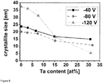
- Fig. 6 it is shown that for -40 V of BIAS the crystallite size is linearly decreasing from ⁇ 24 to ⁇ 15 nm with increasing Ta content; for -80 V decreasing grain sizes between ⁇ 20 to ⁇ 10 nm can be observed.
- the coatings exhibit an unexpectedly large crystallite size of 37, 36, and 31 nm in Ta-free layers and for a Ta content of about 3 at% and 7 at%, respectively and a very small grain size of only ⁇ 5 nm for Ta content of about 31 at%.
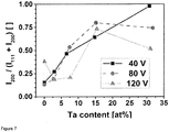
- the preferred orientation of the (Al,Cr,Ta)N coatings on austenite is exemplarily indicated by the peak intensity ratio I 200 /(I 200 +I 111 ) in Fig. 7 .
- a highly 111 preferred orientation can be observed for -40 V of BIAS, which is linearly changing into a 200 orientation with increasing Ta content.
- increasing BIAS voltages e.g. up to -80 V
- other coating parameters such as magnetic field arrangement, pressure or process temperature, can be adjusted in order to intensify the apparent effect.
- a hard coating according to the present invention is particularly good for providing excellent abrasion resistance to surfaces of cutting and forming tools which should be exposed to tribological contact (contact tool-workpiece involving relative motion between the tool surface(s) and the workpiece surface(s) in contact) that involves the generation of elevated temperatures at the surface contact point.
- Coatings according to the present invention that have a crystallite growth with strong preferred orientation [200] and that are particularly good for attaining a high protection of tools used by cutting operations, are preferred. Because of that, the at least one (Al a Cr b Ta c )N layer should be deposited on a substrate surface in such a manner, that depending on the application, the preferred orientation at least in the area near to the coating surface is stronger [200].
- the at least one (Al a Cr b Ta c )N layer hard layer in a hard coating according to the present invention exhibits a peak intensity ratio I 200 /(I 200 +I 111 ) ⁇ 0.25, depending on the application the ratio should be preferably ⁇ 0.35, or more preferably ⁇ 0.50.
- the at least one (Al a Cr b Ta c )N hard layer is deposited on a substrate surface in such a manner that the peak intensity ratio I 200 /(I 200 +I 111 ) ⁇ 0.25 presents a variation along the layer thickness.
- the peak intensity ratio I 200 /(I 200 +I 111 ) in the at least one (Al a Cr b Ta c )N hard layer according the present invention it is lower in the area near to the substrate than in the area near to the coating surface.
- the at least one (Al a Cr b Ta c )N layer is deposited on a substrate surface in such a manner that a residual stress variation along the layer thickness is attained.
- the residual stress should be lower in the area near to the substrate and higher in the area near to the coating surface, depending on the kind of application and/or type of substrate.
- the at least one (Al a Cr b Ta c )N layer is deposited having a polycrystalline structure, preferably a fine crystalline structure.
- the polycrystalline structure can be deposited in such a manner that in the area near to the substrate the average crystallite size is larger than in the area near to the coating surface.
- the at least one (Al a Cr b Ta c )N layer according to the present invention can be deposited having a columnar structure in the area near to the substrate and a polycrystalline structure in the area near to the coating surface.
- the at least one (Al a Cr b Ta c )N layer is deposited having a variable Young's modulus of elasticity.
- the layer can be deposited in order to have a lower Young's Modulus of elasticity in the area near to the substrate than in the area near to the coating surface.
- it could be advantageously to maintain the a high hardness ( ⁇ 35 GPa) along the complete (Al a Cr b Ta c )N layer independently from the Young's Modulus variation.
- a coating according to the present invention can also comprise more than one (Al a Cr b Ta c )N layers, for example one (Al a Cr b Ta c )N lower layer and one (Al a Cr b Ta c )N upper layer.
- the lower layer could for example be deposited having the characteristics of the above described embodiments corresponding to the area of the at least one (Al a Cr b Ta c )N layer near to the substrate and the upper layer could for example be deposited having the characteristics of the above described embodiments corresponding to the area of the at least one (Al a Cr b Ta c )N layer near to the coating surface.
- the present invention also provides a reactive arc ion plating pvd method for depositing hard coatings in a nitrogen reactive atmosphere comprising at least one (Al a Cr b Ta c )N layer according to the present invention, whereby the peak intensity ratio I 200 /(I 200 +I 111 ), the residual stress, the kind of polycrystalline structure, the crystallite size, the Young's modulus of elasticity and the hardness of the coating are adjusted arbitrarily according to the required coating properties by selecting BIAS voltage and tantalum content in AlCrTa targets independently from further coating parameters.
Landscapes
- Chemical & Material Sciences (AREA)
- Engineering & Computer Science (AREA)
- Materials Engineering (AREA)
- Organic Chemistry (AREA)
- Chemical Kinetics & Catalysis (AREA)
- Mechanical Engineering (AREA)
- Metallurgy (AREA)
- Life Sciences & Earth Sciences (AREA)
- Wood Science & Technology (AREA)
- Inorganic Chemistry (AREA)
- Physical Vapour Deposition (AREA)
- Cutting Tools, Boring Holders, And Turrets (AREA)
Description
- The present invention relates to a simple coating system comprising aluminum (Al), chromium (Cr), tantalum (Ta) and nitrogen (N) as main components which provides wear protection to tools and/or components exposed to tribological contact at elevated temperatures. This coating exhibits in particular an excellent chemical and mechanical stability at elevated temperatures. Particularly, the present invention relates to a hard coating comprising at least one layer comprising Al, Cr, Ta and N as main components and having chemical composition regarding these elements according to the formula (AlaCrbTac)N, where a, b and c are respectively the concentration of aluminum, chromium and tantalum in atomic ratio considering only Al, Cr and Ta for the calculation of the element composition in the layer, whereby a = x•(1-c), b = (1-x)•(1-c), 0.60 ≤ x ≤ 0.70, 0.01 ≤ c ≤ 0.5, and the (AlaCrbTac)N layer at least exhibits a X-ray diffraction peak intensity ratio I200/(I200+I111) ≥ 0.25.
- Protecting cutting tools by coating tool surfaces with (Cr,AI,Ta)N hard coatings deposited from CrAlTa-containing targets in a reactive nitrogen atmosphere by using arc ion plating techniques, is an already known practice.
-
JP2006334740A JP2006334740A - Similarly,
JP2007105843A JP2007105843A JP2006334740A - the lower layer should have a single layer structure with chemical composition Cr1-(x+y)AlxTay, with x = 0.50-0.65 and y = 0.01-0.10 in atomic ratio considering only Cr, Al and Ta for the calculation of the element composition in the lower layer, and
- the upper layer should have a multilayer structure comprising two types of layers, A and B, deposited alternated one of each other, and
- the layers A and B should be nanolayers, each one having single layer thickness of about 5-20 nm, and
- each nanolayer A should have chemical composition Cr1-(E+F)AlETaF with E = 0.15-0.30 and F = 0.20-0.35 in atomic ratio considering only Cr, Al and Ta for the calculation of the element composition in the corresponding nanolayer A, and
- each nanolayer B should have chemical composition Cr1-(M+N)AlMTaN with M = 0.50-0.65 and N = 0.01-0.10 in atomic ratio considering only Cr, Al and Ta for the calculation of the element composition in the corresponding nanolayer B.
- However, the complex constitution of the aforementioned (Cr,Al,Ta)N hard coatings which requires the deposition of different layers and nanolayers having defined layer thicknesses as well as different element compositions along the complete coating constitution results in very high requirements regarding complexity of the coating process. A high risk of confusion of the targets having different compositions is also one disadvantage by depositing the aforementioned (Cr,Al,Ta)N hard coatings. One more disadvantage by the deposition of the aforementioned (Cr,Al,Ta)N hard coatings is the difficulty of depositing nanolayers one by one which should have completely different element compositions regardless of the very small required nanolayer thicknesses (about 5-20 nm), in particular if different kind of tools (e.g. tools having different dimensions and/or geometries) must be coated.
- Main objective of the present invention is to provide a (Cr,Al,Ta)N hard coating having a simple coating constitution, particularly in comparison with the aforementioned (Cr,Al,Ta)N hard coating according to the state of the art but providing also excellent wear resistance to tools used in high speed cutting of highly reactive materials.
- The aforementioned objective is achieved by the present invention by providing a hard coating according to
claim 1. - A hard coating according to the present invention comprises at least one layer comprising chromium, aluminum tantalum and nitrogen at least as main components and having chemical composition regarding these elements according to the formula: (AlaCrbTac)N, where a, b and c are respectively the concentration of aluminum, chromium and tantalum in atomic ratio considering only Al, Cr and Ta for the calculation of the element composition in the layer, whereby:
- a = x·(1-c),
- b = (1-x)·(1-c), and
- 0.60 ≤ x ≤ 0.70, and
- 0.01 ≤ c ≤ 0.5, and
- wherein 0.44 ≤ a ≤ 0.66 and
- where at least one (AlaCrbTac)N layer exhibits a X-ray diffraction peak intensity ratio I200/(I200+I111) ≥ 0.25, wherein said peak intensity ratio presents a variation along the layer thickness in such a manner that it is lower in the area near to the substrate than in the area near to the coating surface.
- The present invention will be explained hereinafter in more detail by means of some examples:
- Different hard coatings according to the present invention were deposited in an INNOVA Balzers arc evaporation plant in a reactive nitrogen atmosphere.
- Four different kinds of targets comprising aluminum, chromium and tantalum and differing in nominal chemical composition in atomic ratio, were used for conducting the experiments. The following chemical compositions were used for depositing corresponding (AlaCrbTac)N layers:
- Al0.686Cr0.294Ta0.020,
- Al0.665Cr0.285Ta0.050,
- Al0.630Cr0.270Ta0.100 and
- Al0.560Cr0.240Ta0.200
- Also, tantalum free targets comprising aluminum and chromium and having nominal chemical composition in atomic ratio of Al0.70Cr0.30 were used for depositing (Al,Cr)N layers.
- The (AlaCrbTac)N and (Al,Cr)N coating layers were deposited by using reactive arc ion plating deposition techniques, the aforementioned targets were arced in nitrogen reactive atmosphere during 60 min for the formation of the corresponding coating layers. The coatings were deposited on 4 different kind of substrates: 1) Si (100), 2) iron foil (1.0330), 3) S600 high speed steel, and 4) austenite, by using an arc current of 150 A, a nitrogen pressure of 3.5 Pa and a negative BIAS of -40, -80, and-120 V.
- A Zeiss EVO50 scanning electron microscope (SEM) was used for examining surface and cross sectional images. The chemical composition was determined with the attached Oxford Instruments INCA energy dispersive X-ray spectroscopy (EDX) system. For investigating structure of the cross sections in the nm range a FEI TECNAI G20 transmission electron microscope (TEM) was used. Structural investigations were carried out on a PANalytical X'pert diffractometer in Bragg Brentano geometry and with CuKa radiation. A CSIRO UMIS nano indentation system by Fischer Cripps Laboratories was used for obtaining load displacement curves with a maximal load between 12 and 30 mN. These curves were evaluated after Oliver and Pharr to determine the hardness and Young's modulus values.
- Table 1 shows a comparison between the chemical compositions of the different target materials and the corresponding (Al,Cr,Ta)N coatings deposited at a BIAS voltage of -40, -80, and -120 V.
- The ratio Al/(Al+Cr) in atomic percentage corresponding to the (Al,Cr)N coatings deposited from the tantalum free targets having chemical composition Al0.70Cr0.30 was about 66 at% (lower than 70 at%).
- By using Ta-containing targets, it was observed that by increasing Ta content in the targets of up to 20 at% a diminution of Al in the deposited layers is detected and consequently, the Al/(Al+Cr) ratio decreases to about 63 at% even though the ratio Al/(Al+Cr) in the targets was maintained constant at about 70 at%.
- Contrariwise, the Ta content in the deposited layers is about 50 % higher than the corresponding Ta content in the targets used for their deposition.
- The nitrogen content of the (Al,Cr,Ta)N coatings tends to be slightly over-stoichiometric and increases by increasing BIAS voltage and Ta content as it is shown in
figure 1 . However, for simplifying the labeling of the different coatings for presenting the results of the examinations, the nitrogen content was normalized forTable 1: Chemical composition of the different sets of Al-Cr-Ta targets and the corresponding metal sublattice compositions of the deposited (Al,Cr,Ta)N coatings at a BIAS voltage of -40, -80, and -120 V. target: composition coating: metal sublattice composition Cr [at%] Al [at%] Ta [at%] Al/(Cr+Al) [at%] BIAS [V] Cr [at%] Al [at%] Ta [at%] Al/(Cr+Al) [at%] label -40 33.5 66.5 - 66.5 30 70 - 70 -80 34.2 65.8 - 65.8 Cr0.34Al0.66N -120 34.7 65.3 - 65.3 -40 33.2 64.0 2.8 65.8 29.4 68.6 2 70 -80 33.7 63.5 2.8 65.3 Cr0.33Al0.64Ta0.03N -120 33.8 63.2 2.9 65.2 -40 33.3 60.2 6.5 64.4 28.5 66.5 5 70 -80 32.2 60.4 7.4 65.3 Cr0.33Al0.60Ta0.07N -120 32.7 59.7 7.6 64.6 -40 30.7 53.9 15.4 63.8 27 63 10 70 -80 29.5 55.4 15.1 65.2 Cr0.30Al0.55Ta0.15N -120 29.9 55.3 14.8 65.0 -40 25.2 43.8 31.0 63.5 24 56 20 70 -80 25.6 42.7 31.7 62.6 Cr0.25Al0.44Ta0.31N -120 25.3 43.9 30.8 63.5 - Figure captions:
-
Figure 1 : Nitrogen content of (Al,Cr,Ta)N coatings with increasing Ta content and for BIAS voltages of -40, -80, and -120 V. -
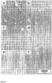
Figure 2 : Surface images of (a, b) Cr0.34Al0.66N, (c, d) Cr0.33Al0.60Ta0.07N and (e, f) Cr0.25Al0.44Ta0.31N coatings deposited on S600 high speed steel at BIAS voltages of -40 and -120 V, respectively. -
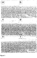
Figure 3 : Cross sectional micrographs of (a, b) Cr0.34Al0.66N, (c, d) Cr0.33Al0.60Ta0.07N and (e, f) Cr0.25Al0.44Ta0.31N coatings deposited on S600 high speed steel at BIAS voltages of -40 and -120 V, respectively. -
Figure 4 : TEM bright-field images of Cr0.34Al0.66N (a) and Cr0.25Al0.44Ta0.31N (b) deposited at -40 V of BIAS. Arrows indicate under-dense column boundaries. -
Figure 5 : Experimentally obtained lattice parameters for BIAS voltages of -40, -80, and -120 V in comparison with ab initio calculated lattice parameters of (AI,Cr,Ta)N coatings. -
Figure 6 : Crystallite size of (Al,Cr,Ta)N coatings obtained by a quadratic Williamson Hall plot from powder diffraction patterns. -
Figure 7 : Texture coefficient of (Al,Cr,Ta)N coatings on austenite in dependency of the Ta content and BIAS voltage. -
Figure 8 : Indentation modulus of (Al,Cr, Ta)N coatings on S600 high speed steel in dependency of the Ta content y and BIAS voltage. -
Figure 9 : Hardness of (Al,Cr, Ta)N coatings on S600 high speed steel in dependency of the Ta content y and BIAS voltage. - SEM Surface images of selected samples of (Al,Cr,Ta)N coatings are shown in
figure 2 . Cr0.34Al0.66N deposited at -40 V of BIAS (fig. 2a ) exhibits a rough surface with droplets the size of ∼1 um in diameter and also a huge amount of smaller droplets. With increasing the Ta content to 7 at% on the metal sublattice (Cr0.33Al060Ta007N,Fig. 2c ), the size and amount of droplets decreases significantly and for even higher contents of 31 at% of Ta (Cr0.25Al044Ta031N, Fig. 6.2e), the film surface appears very homogenous and flat with just a few droplets on top (max. diameter -0.5 µm). Increasing the BIAS voltage to -120 V leads to a clear improvement of the surface morphology of Cr034Al0 66N (seefig. 2b ). Nevertheless, the effect of an increased BIAS voltage seems to be less pronounced for Ta alloyed Cr0.33Al0.60Ta0.07N (fig. 2d ) and not detectable for Cr0.25Al0.44Ta0.31N (fig. 2f ). Decreasing droplet densities with increasing Ta content could be based on the formation of intermetallic phases on the target surface which lead to an increased melting point of the target material and hence decreased droplet formation. However, the heavy Ta atom (compare: Ta ∼181 g/mol, Ti ∼48 g/mol, and Al ∼27 g/mol) might have a significant "etching" (or resputtering) effect on the substrate surface and hence even at -40 V of BIAS small droplets could be atomized and large droplets significantly etched. The resputtering effect is, besides densification, a possible reason for decreasing film thicknesses from ∼2.7 to ∼2.3 um with increasing the Ta content from 0 to 31 at% and decreasing thicknesses of up to ∼0.2 um with increasing the BIAS voltage from -40 to -120 V. Corresponding fracture cross-sectional micrographs exhibit a columnar structure for Ta-free Cr0.34Al0.66N (fig. 3a and b ). This columnar structure appears much less pronounced for Cr0.33Al0.60Ta0.07N (fig. 3c and d ) and at very high Ta contents like for Cr0.25Al0.44Ta0.31N the fracture surface is very smooth and columns can hardly be detected. A clear influence of the BIAS voltage cannot be observed for the fracture cross-sections-compare therefor the -40 and -120 V images offigs. 3a, c, e and Figs. 3b, d, f , respectively. However, TEM investigations of Cr0.34Al0.66N deposited at -40 V BIAS exhibit a columnar structure with a column size of around 50 nm, seeFig. 4a . At the column boundaries under-dense areas can be detected (indicated by the arrows). In contrary, for very high Ta contents like for Cr0.25Al0.44Ta0.31N (Fig. 4b ) the columnar structure is not fully developed and open column- or grain- boundaries cannot be observed. Due to the two-fold rotation of our samples mounted to the carousel and the high mass difference of the used elements, also a layered structure develops even if the coating is deposited from equal composite targets. In this case of bright-field images, the dark layer regions are enriched by heavy elements and the bright ones by light elements. Increasing BIAS voltages and atomic masses leads in general to an increase of the etching power. The TEM images presented inFig. 4 clearly indicate that the heavy Ta can improve the density of the coating (especially column boundaries) even at -40 V of BIAS and for all different investigated Ta contents. - Ab initio calculated lattice parameters (star symbols in
fig. 5 ) indicate an increasing lattice parameter with increasing Ta-content, which is confirmed by the experimental data of the (Al,Cr,Ta)N coatings inFig. 5 . - The BIAS voltage and the Ta content are of course also influencing the grain size of the (Al,Cr,Ta)N coatings. In
Fig. 6 it is shown that for -40 V of BIAS the crystallite size is linearly decreasing from ∼24 to ∼15 nm with increasing Ta content; for -80 V decreasing grain sizes between ∼20 to ∼10 nm can be observed. However, at a BIAS voltage of -120 V, the coatings exhibit an unexpectedly large crystallite size of 37, 36, and 31 nm in Ta-free layers and for a Ta content of about 3 at% and 7 at%, respectively and a very small grain size of only ∼5 nm for Ta content of about 31 at%. - Further, by increasing the amount of Ta in the layers up to 15 and 31 at%, it is possible to form layers having crystallites with a crystallite size of about 17 and about 5 nm, respectively.
- The preferred orientation of the (Al,Cr,Ta)N coatings on austenite is exemplarily indicated by the peak intensity ratio I200/(I200+I111) in
Fig. 7 . For Ta-free Cr0.34Al0.66N a highly 111 preferred orientation can be observed for -40 V of BIAS, which is linearly changing into a 200 orientation with increasing Ta content. In this case, increasing BIAS voltages (e.g. up to -80 V) do not significantly influence this tendency. However, also other coating parameters, such as magnetic field arrangement, pressure or process temperature, can be adjusted in order to intensify the apparent effect. - The change of texture with increasing Ta-content in the coatings goes along with a decrease in grain size, as to be seen in
Fig. 6 . - SEM and TEM cross sections and the grain size analysis (
figs. 3 ,4 and6 ) also suggest that with increasing Ta content film growth mechanisms are substantially influenced. For low Ta contents, mainly columnar growth can be observed, whereas the nano-crystalline growth could be attained by using higher Ta contents (-31 at%) on the metal sublattice as an alternative to high BIAS voltages of > -120 V for Ta-free (Al,Cr)N coatings. - An additional effect of adding Ta in (Al,Cr)N and/or increasing Ta content in (Al,Cr)N coating according to the present invention is the attainment of smaller Young's modulus. In
Fig. 8 it can be observed that the indentation modulus for Ta-free Cr0.34Al0.66N at a BIAS voltage of -40 V clearly deviates from the general trend. This can be explained as a consequence of the under-dense grain boundaries observed in the cross sectional TEM images corresponding to this coating inFig. 4a . - It can be that the grain boundary bonding is less developed and leads directly to a reduced indentation modulus. The orientation dependent decrease of the Young's modulus is probably for a big part directly reflected in the measured decreasing indentation moduli. As we have observed a slight increase in nitrogen content with increasing BIAS and Ta-content, this might also be a reason for decreasing indentation moduli. The weakening effect due to under-dense grain boundaries can also be observed for the hardness of the -40 V BIAS Cr0.34Al0.66N and Cr0.33Al0.64Ta0.03N coatings, see
Fig. 9 , as the reduced bonding also decreases their measured hardness. Overall, we can see slightly decreasing hardness values with increasing Ta-content. Considering plasticity indexes like H/E and in combination with the decreasing indentation moduli, strongly increasing ability for plastic deformation at still high hardness can be expected for high Ta-containing coatings like Cr0.30Al0.55Ta0.15N or Cr0.25Al0.44Ta0.31N. - Surface SEM images reveal decreasing droplet densities with increasing the BIAS voltage for coatings having chemical composition in atomic ratio of Cr0.34Al0.66N. However, additions of Ta are even at -40 V of BIAS significantly more effective and lead to a very smooth surface with a few large droplets on top. The cross sectional micrographs obtained by SEM and TEM exhibit a columnar structure with under-dense grain boundaries and an XRD evaluated crystallite size of ∼ 25 nm for Ta-free Cr0.34Al0.66N coatings deposited by using a BIAS of -40 V. With increasing the Ta-content, the grain-boundaries densifies, the columnar structure is less pronounced and the crystallite size decreases towards 20 nm. For Cr0.25Al0.44Ta0.31N deposited by using a BIAS of -120 V the crystallite size is reduced to ∼5 nm. Considering the preferred orientation of growth of the deposited coatings, it can be seen a clear trend from oriented growth [111] for Ta-free coatings to a [200] dominated growth with increasing Ta-content. The change in preferred orientation has a significant influence on the measured indentation moduli of the coatings according to the present invention which decrease by -125 GPa with increasing Ta content. However, the hardness stays more or less constant at values >35 GPa and hence, a significant increase in plasticity at still high hardness values can be expected. Alloying Ta to high-AI containing single phase cubic (Cr,Al)N according to the present invention allows attaining significantly improved mechanical and structural properties at elevated temperatures.
- A hard coating according to the present invention is particularly good for providing excellent abrasion resistance to surfaces of cutting and forming tools which should be exposed to tribological contact (contact tool-workpiece involving relative motion between the tool surface(s) and the workpiece surface(s) in contact) that involves the generation of elevated temperatures at the surface contact point.
- Coatings according to the present invention that have a crystallite growth with strong preferred orientation [200] and that are particularly good for attaining a high protection of tools used by cutting operations, are preferred. Because of that, the at least one (AlaCrbTac)N layer should be deposited on a substrate surface in such a manner, that depending on the application, the preferred orientation at least in the area near to the coating surface is stronger [200].
- As it was described above, the at least one (AlaCrbTac)N layer hard layer in a hard coating according to the present invention exhibits a peak intensity ratio I200/(I200+I111) ≥ 0.25, depending on the application the ratio should be preferably ≥ 0.35, or more preferably ≥ 0.50.
- According to the present invention, the at least one (AlaCrbTac)N hard layer is deposited on a substrate surface in such a manner that the peak intensity ratio I200/(I200+I111) ≥ 0.25 presents a variation along the layer thickness.
- The peak intensity ratio I200/(I200+I111) in the at least one (AlaCrbTac)N hard layer according the present invention it is lower in the area near to the substrate than in the area near to the coating surface.
- According to a preferred embodiment of the present invention, the at least one (AlaCrbTac)N layer is deposited on a substrate surface in such a manner that a residual stress variation along the layer thickness is attained.
- According to a preferred embodiment of a coating having a (AlaCrbTac)N layer with variable residual stress, the residual stress should be lower in the area near to the substrate and higher in the area near to the coating surface, depending on the kind of application and/or type of substrate.
- According to another preferred embodiment of the present invention, the at least one (AlaCrbTac)N layer is deposited having a polycrystalline structure, preferably a fine crystalline structure. Furthermore, the polycrystalline structure can be deposited in such a manner that in the area near to the substrate the average crystallite size is larger than in the area near to the coating surface. Also, the at least one (AlaCrbTac)N layer according to the present invention can be deposited having a columnar structure in the area near to the substrate and a polycrystalline structure in the area near to the coating surface.
- According to another preferred embodiment of the present invention, the at least one (AlaCrbTac)N layer is deposited having a variable Young's modulus of elasticity. For example, the layer can be deposited in order to have a lower Young's Modulus of elasticity in the area near to the substrate than in the area near to the coating surface. For some applications it could be advantageously to maintain the a high hardness (≥ 35 GPa) along the complete (AlaCrbTac)N layer independently from the Young's Modulus variation.
- A coating according to the present invention can also comprise more than one (AlaCrbTac)N layers, for example one (AlaCrbTac)N lower layer and one (AlaCrbTac)N upper layer. In this case, the lower layer could for example be deposited having the characteristics of the above described embodiments corresponding to the area of the at least one (AlaCrbTac)N layer near to the substrate and the upper layer could for example be deposited having the characteristics of the above described embodiments corresponding to the area of the at least one (AlaCrbTac)N layer near to the coating surface.
- The present invention also provides a reactive arc ion plating pvd method for depositing hard coatings in a nitrogen reactive atmosphere comprising at least one (AlaCrbTac)N layer according to the present invention, whereby the peak intensity ratio I200/(I200+I111), the residual stress, the kind of polycrystalline structure, the crystallite size, the Young's modulus of elasticity and the hardness of the coating are adjusted arbitrarily according to the required coating properties by selecting BIAS voltage and tantalum content in AlCrTa targets independently from further coating parameters.
Claims (11)
- Hard coating comprising at least one layer comprising chromium, aluminum tantalum and nitrogen as main components and having chemical composition regarding these elements according to the formula: (AlaCrbTac)N,
where the coefficients a, b and c are respectively of the concentration of aluminum, chromium and tantalum in atomic ratio considering only Al, Cr and Ta for the calculation of the element composition in the layer, characterized by the at least one layer having element composition (AlaCrbTac)N layer:- has coefficients a, b and c satisfying following conditions:∘ a = x·(1-c),∘ b = (1-x)·(1-c),∘ 0.60 ≤ x ≤ 0.70,∘ 0.01 ≤ c ≤ 0.5,∘ wherein 0.44 ≤ a ≤ 0.66,and- exhibits a X-ray diffraction peak intensity ratio I200/(I200+I111) ≥ 0.25, wherein said peak intensity ratio presents a variation along the layer thickness in such a manner that it is lower in the area near to the substrate than in the area near to the coating surface. - Hard coating according to claim 1, characterized by a peak intensity ratio I200/(I200+I111) ≥ 0.50.
- Hard coating according to at least one of the previous claims 1 or 2, characterized by the at least one layer having element composition (AlaCrbTac)N layer having a variable residual stress along the layer thickness.
- Hard coating according to claim 3, characterized in that the residual stress in the area near to the substrate is lower than in the area near to the coating surface.
- Hard coating according to at least one of the previous claims 1 to 4, characterized by the at least one layer having element composition (AlaCrbTac)N layer exhibiting a polycrystalline structure.
- Hard coating according to at least one of the previous claims 1 to 4, characterized by the at least one layer having element composition (AlaCrbTac)N layer exhibiting a structure which combines a columnar structure in the area near to the substrate with a fine polycrystalline structure in the area near to the coating surface.
- Hard coating according to claim 5, characterized in that, the polycrystalline structure exhibits crystallites having different grain sizes, whereby in the area near to the surface coating the average size of the crystallites is smaller than in the area near to the substrate.
- Hard coating according to at least one of the previous claims 1 to 7, characterized by the at least one layer having element composition (AlaCrbTac)N layer having a variable Young's modulus of elasticity along the layer thickness.
- Hard coating according to at least one of the previous claims 1 to 8, characterized by having a hardness ≥ 32 GPa along the complete (AlaCrbTac)N layer.
- Hard coating according to at least one of the previous claims, characterized by comprising more than one (AlaCrbTac)N layer.
- Reactive arc ion plating pvd method for depositing a hard coating according to at least one of the previous claims, characterized in that:• the deposition of the at least one (AlaCrbTac)N layer is carried out from AlCrTA targets in a nitrogen reactive atmosphere, and• the coating properties regarding peak intensity ratio I200/(I200+I111), residual stress, kind of polycrystalline structure, crystallite size, Young's modulus of elasticity and coating hardness are adjusted by selecting deposition temperature, pressure, BIAS voltage and tantalum content in the AlCrTa targets.
Applications Claiming Priority (2)
| Application Number | Priority Date | Filing Date | Title |
|---|---|---|---|
| DE102013018867.9A DE102013018867A1 (en) | 2013-11-12 | 2013-11-12 | (Al, Cr, Ta) N-coating for improved temperature resistance |
| PCT/EP2014/002996 WO2015070967A1 (en) | 2013-11-12 | 2014-11-10 | (al,cr,ta)n coating for enhanced high temperature resistance |
Publications (2)
| Publication Number | Publication Date |
|---|---|
| EP3068920A1 EP3068920A1 (en) | 2016-09-21 |
| EP3068920B1 true EP3068920B1 (en) | 2019-04-03 |
Family
ID=51868934
Family Applications (1)
| Application Number | Title | Priority Date | Filing Date |
|---|---|---|---|
| EP14795782.3A Active EP3068920B1 (en) | 2013-11-12 | 2014-11-10 | (al,cr,ta)n coating for enhanced high temperature resistance |
Country Status (4)
| Country | Link |
|---|---|
| US (1) | US9885106B2 (en) |
| EP (1) | EP3068920B1 (en) |
| DE (1) | DE102013018867A1 (en) |
| WO (1) | WO2015070967A1 (en) |
Families Citing this family (3)
| Publication number | Priority date | Publication date | Assignee | Title |
|---|---|---|---|---|
| DE102012200378A1 (en) * | 2012-01-12 | 2013-07-18 | Federal-Mogul Burscheid Gmbh | piston ring |
| CN116988009B (en) * | 2023-07-11 | 2025-12-09 | 上海应用技术大学 | CrAlTaN multilayer gradient coating and preparation method and application thereof |
| CN121380838A (en) * | 2025-12-19 | 2026-01-23 | 厦门理工学院 | A tantalum-doped nitride coating and its preparation method |
Family Cites Families (7)
| Publication number | Priority date | Publication date | Assignee | Title |
|---|---|---|---|---|
| DE10233222B4 (en) * | 2001-07-23 | 2007-03-01 | Kabushiki Kaisha Kobe Seiko Sho (Kobe Steel, Ltd.), Kobe | Hard wear-resistant layer, method of forming same and use |
| US8318328B2 (en) * | 2004-07-15 | 2012-11-27 | Oerlikon Trading Ag, Trubbach | High oxidation resistant hard coating for cutting tools |
| JP2006334740A (en) | 2005-06-03 | 2006-12-14 | Mitsubishi Materials Corp | Cutting tool made of surface-coated cemented carbide that provides excellent wear resistance with a hard coating layer in high-speed cutting of highly reactive materials |
| JP2007105843A (en) | 2005-10-14 | 2007-04-26 | Mitsubishi Materials Corp | Surface-coated cutting tool that exhibits high wear resistance with a hard coating layer in high-speed cutting of highly reactive materials |
| NZ575279A (en) * | 2006-09-26 | 2012-05-25 | Oerlikon Trading Ag | Metal cutting tools with hard coating applied by a physical vapour deposition process |
| WO2010150411A1 (en) * | 2009-06-26 | 2010-12-29 | オーエスジー株式会社 | Hard coating film and tool coated with hard coating film |
| JP5459618B2 (en) * | 2010-04-20 | 2014-04-02 | 三菱マテリアル株式会社 | Surface coated cutting tool |
-
2013
- 2013-11-12 DE DE102013018867.9A patent/DE102013018867A1/en not_active Withdrawn
-
2014
- 2014-11-10 EP EP14795782.3A patent/EP3068920B1/en active Active
- 2014-11-10 WO PCT/EP2014/002996 patent/WO2015070967A1/en not_active Ceased
- 2014-11-10 US US15/034,904 patent/US9885106B2/en active Active
Non-Patent Citations (1)
| Title |
|---|
| None * |
Also Published As
| Publication number | Publication date |
|---|---|
| DE102013018867A1 (en) | 2015-06-25 |
| US9885106B2 (en) | 2018-02-06 |
| US20160348228A1 (en) | 2016-12-01 |
| EP3068920A1 (en) | 2016-09-21 |
| WO2015070967A1 (en) | 2015-05-21 |
Similar Documents
| Publication | Publication Date | Title |
|---|---|---|
| EP2893052B1 (en) | Ti-al-ta-based coating exhibiting enhanced thermal stability | |
| KR102027610B1 (en) | Coated cutting tool and method of making the same | |
| Braic et al. | Nanostructured multi-element (TiZrNbHfTa) N and (TiZrNbHfTa) C hard coatings | |
| KR101515652B1 (en) | Abrasion-resistant hard coating for a workpiece and method for manufacturing the same | |
| RU2560480C2 (en) | CUTTING TOOLS WITH SANDWICHED COATINGS OF Al-Cr-B/Ti-Al-N | |
| CN111511490B (en) | Clad Cutting Tools | |
| KR101278385B1 (en) | Coated tool | |
| US8409696B2 (en) | Multilayered coated cutting tool | |
| Fernandes et al. | The effect of increasing V content on the structure, mechanical properties and oxidation resistance of Ti–Si–V–N films deposited by DC reactive magnetron sputtering | |
| CA2973927C (en) | High performance coating for high-strength steel cold metal forming | |
| KR20170059421A (en) | Coated cutting tool | |
| Mei et al. | Greater improvement of carbon and boron co-doping on the mechanical properties, wear resistance and cutting performance of AlTiN coating than that of doping alone | |
| KR102956212B1 (en) | cutting tool | |
| Malinovskis et al. | Synthesis and characterisation of Mo-BC thin films deposited by non-reactive DC magnetron sputtering | |
| JP5450400B2 (en) | Al-Ti-Ru-N-C hard material coating | |
| US9885106B2 (en) | (Al, Cr, Ta)N coating for enhanced high temperature resistance | |
| US20140373751A1 (en) | Niobium-based coatings, methods of producing same, and apparatus including same | |
| KR20130006347A (en) | Coated article having yttrium-containing coatings applied by physical vapor deposition and method for making the same | |
| DE102010038077B4 (en) | Indexable insert and process for its production | |
| JP7170965B2 (en) | Cemented Carbide and Coated Cemented Carbide | |
| Zhang et al. | Toughness enhancement mechanism of Ni-doped Cr2N | |
| Zhang et al. | Microstructure, chemical states, and mechanical properties of V–C–Co coatings prepared by non-reactive magnetron sputtering | |
| KR20190099394A (en) | film | |
| EP2434032A1 (en) | Coated fine grained cermet for finish turning applications | |
| EP3254787A1 (en) | Hard coating film |
Legal Events
| Date | Code | Title | Description |
|---|---|---|---|
| PUAI | Public reference made under article 153(3) epc to a published international application that has entered the european phase |
Free format text: ORIGINAL CODE: 0009012 |
|
| 17P | Request for examination filed |
Effective date: 20160512 |
|
| AK | Designated contracting states |
Kind code of ref document: A1 Designated state(s): AL AT BE BG CH CY CZ DE DK EE ES FI FR GB GR HR HU IE IS IT LI LT LU LV MC MK MT NL NO PL PT RO RS SE SI SK SM TR |
|
| AX | Request for extension of the european patent |
Extension state: BA ME |
|
| DAX | Request for extension of the european patent (deleted) | ||
| STAA | Information on the status of an ep patent application or granted ep patent |
Free format text: STATUS: EXAMINATION IS IN PROGRESS |
|
| 17Q | First examination report despatched |
Effective date: 20170703 |
|
| GRAP | Despatch of communication of intention to grant a patent |
Free format text: ORIGINAL CODE: EPIDOSNIGR1 |
|
| STAA | Information on the status of an ep patent application or granted ep patent |
Free format text: STATUS: GRANT OF PATENT IS INTENDED |
|
| INTG | Intention to grant announced |
Effective date: 20180524 |
|
| GRAJ | Information related to disapproval of communication of intention to grant by the applicant or resumption of examination proceedings by the epo deleted |
Free format text: ORIGINAL CODE: EPIDOSDIGR1 |
|
| STAA | Information on the status of an ep patent application or granted ep patent |
Free format text: STATUS: EXAMINATION IS IN PROGRESS |
|
| GRAP | Despatch of communication of intention to grant a patent |
Free format text: ORIGINAL CODE: EPIDOSNIGR1 |
|
| STAA | Information on the status of an ep patent application or granted ep patent |
Free format text: STATUS: GRANT OF PATENT IS INTENDED |
|
| INTC | Intention to grant announced (deleted) | ||
| INTG | Intention to grant announced |
Effective date: 20181010 |
|
| GRAS | Grant fee paid |
Free format text: ORIGINAL CODE: EPIDOSNIGR3 |
|
| GRAA | (expected) grant |
Free format text: ORIGINAL CODE: 0009210 |
|
| STAA | Information on the status of an ep patent application or granted ep patent |
Free format text: STATUS: THE PATENT HAS BEEN GRANTED |
|
| AK | Designated contracting states |
Kind code of ref document: B1 Designated state(s): AL AT BE BG CH CY CZ DE DK EE ES FI FR GB GR HR HU IE IS IT LI LT LU LV MC MK MT NL NO PL PT RO RS SE SI SK SM TR |
|
| REG | Reference to a national code |
Ref country code: GB Ref legal event code: FG4D |
|
| REG | Reference to a national code |
Ref country code: CH Ref legal event code: EP Ref country code: AT Ref legal event code: REF Ref document number: 1115832 Country of ref document: AT Kind code of ref document: T Effective date: 20190415 |
|
| REG | Reference to a national code |
Ref country code: DE Ref legal event code: R096 Ref document number: 602014044092 Country of ref document: DE |
|
| REG | Reference to a national code |
Ref country code: IE Ref legal event code: FG4D |
|
| REG | Reference to a national code |
Ref country code: NL Ref legal event code: FP |
|
| REG | Reference to a national code |
Ref country code: SE Ref legal event code: TRGR |
|
| REG | Reference to a national code |
Ref country code: LT Ref legal event code: MG4D |
|
| PG25 | Lapsed in a contracting state [announced via postgrant information from national office to epo] |
Ref country code: NO Free format text: LAPSE BECAUSE OF FAILURE TO SUBMIT A TRANSLATION OF THE DESCRIPTION OR TO PAY THE FEE WITHIN THE PRESCRIBED TIME-LIMIT Effective date: 20190703 Ref country code: CZ Free format text: LAPSE BECAUSE OF FAILURE TO SUBMIT A TRANSLATION OF THE DESCRIPTION OR TO PAY THE FEE WITHIN THE PRESCRIBED TIME-LIMIT Effective date: 20190403 Ref country code: ES Free format text: LAPSE BECAUSE OF FAILURE TO SUBMIT A TRANSLATION OF THE DESCRIPTION OR TO PAY THE FEE WITHIN THE PRESCRIBED TIME-LIMIT Effective date: 20190403 Ref country code: LT Free format text: LAPSE BECAUSE OF FAILURE TO SUBMIT A TRANSLATION OF THE DESCRIPTION OR TO PAY THE FEE WITHIN THE PRESCRIBED TIME-LIMIT Effective date: 20190403 Ref country code: PT Free format text: LAPSE BECAUSE OF FAILURE TO SUBMIT A TRANSLATION OF THE DESCRIPTION OR TO PAY THE FEE WITHIN THE PRESCRIBED TIME-LIMIT Effective date: 20190803 Ref country code: HR Free format text: LAPSE BECAUSE OF FAILURE TO SUBMIT A TRANSLATION OF THE DESCRIPTION OR TO PAY THE FEE WITHIN THE PRESCRIBED TIME-LIMIT Effective date: 20190403 Ref country code: AL Free format text: LAPSE BECAUSE OF FAILURE TO SUBMIT A TRANSLATION OF THE DESCRIPTION OR TO PAY THE FEE WITHIN THE PRESCRIBED TIME-LIMIT Effective date: 20190403 Ref country code: FI Free format text: LAPSE BECAUSE OF FAILURE TO SUBMIT A TRANSLATION OF THE DESCRIPTION OR TO PAY THE FEE WITHIN THE PRESCRIBED TIME-LIMIT Effective date: 20190403 |
|
| PG25 | Lapsed in a contracting state [announced via postgrant information from national office to epo] |
Ref country code: LV Free format text: LAPSE BECAUSE OF FAILURE TO SUBMIT A TRANSLATION OF THE DESCRIPTION OR TO PAY THE FEE WITHIN THE PRESCRIBED TIME-LIMIT Effective date: 20190403 Ref country code: GR Free format text: LAPSE BECAUSE OF FAILURE TO SUBMIT A TRANSLATION OF THE DESCRIPTION OR TO PAY THE FEE WITHIN THE PRESCRIBED TIME-LIMIT Effective date: 20190704 Ref country code: PL Free format text: LAPSE BECAUSE OF FAILURE TO SUBMIT A TRANSLATION OF THE DESCRIPTION OR TO PAY THE FEE WITHIN THE PRESCRIBED TIME-LIMIT Effective date: 20190403 Ref country code: BG Free format text: LAPSE BECAUSE OF FAILURE TO SUBMIT A TRANSLATION OF THE DESCRIPTION OR TO PAY THE FEE WITHIN THE PRESCRIBED TIME-LIMIT Effective date: 20190703 Ref country code: RS Free format text: LAPSE BECAUSE OF FAILURE TO SUBMIT A TRANSLATION OF THE DESCRIPTION OR TO PAY THE FEE WITHIN THE PRESCRIBED TIME-LIMIT Effective date: 20190403 |
|
| PG25 | Lapsed in a contracting state [announced via postgrant information from national office to epo] |
Ref country code: IS Free format text: LAPSE BECAUSE OF FAILURE TO SUBMIT A TRANSLATION OF THE DESCRIPTION OR TO PAY THE FEE WITHIN THE PRESCRIBED TIME-LIMIT Effective date: 20190803 |
|
| REG | Reference to a national code |
Ref country code: DE Ref legal event code: R097 Ref document number: 602014044092 Country of ref document: DE |
|
| PG25 | Lapsed in a contracting state [announced via postgrant information from national office to epo] |
Ref country code: SK Free format text: LAPSE BECAUSE OF FAILURE TO SUBMIT A TRANSLATION OF THE DESCRIPTION OR TO PAY THE FEE WITHIN THE PRESCRIBED TIME-LIMIT Effective date: 20190403 Ref country code: RO Free format text: LAPSE BECAUSE OF FAILURE TO SUBMIT A TRANSLATION OF THE DESCRIPTION OR TO PAY THE FEE WITHIN THE PRESCRIBED TIME-LIMIT Effective date: 20190403 Ref country code: DK Free format text: LAPSE BECAUSE OF FAILURE TO SUBMIT A TRANSLATION OF THE DESCRIPTION OR TO PAY THE FEE WITHIN THE PRESCRIBED TIME-LIMIT Effective date: 20190403 Ref country code: EE Free format text: LAPSE BECAUSE OF FAILURE TO SUBMIT A TRANSLATION OF THE DESCRIPTION OR TO PAY THE FEE WITHIN THE PRESCRIBED TIME-LIMIT Effective date: 20190403 |
|
| PLBE | No opposition filed within time limit |
Free format text: ORIGINAL CODE: 0009261 |
|
| STAA | Information on the status of an ep patent application or granted ep patent |
Free format text: STATUS: NO OPPOSITION FILED WITHIN TIME LIMIT |
|
| PG25 | Lapsed in a contracting state [announced via postgrant information from national office to epo] |
Ref country code: SM Free format text: LAPSE BECAUSE OF FAILURE TO SUBMIT A TRANSLATION OF THE DESCRIPTION OR TO PAY THE FEE WITHIN THE PRESCRIBED TIME-LIMIT Effective date: 20190403 |
|
| 26N | No opposition filed |
Effective date: 20200106 |
|
| PG25 | Lapsed in a contracting state [announced via postgrant information from national office to epo] |
Ref country code: TR Free format text: LAPSE BECAUSE OF FAILURE TO SUBMIT A TRANSLATION OF THE DESCRIPTION OR TO PAY THE FEE WITHIN THE PRESCRIBED TIME-LIMIT Effective date: 20190403 |
|
| PGFP | Annual fee paid to national office [announced via postgrant information from national office to epo] |
Ref country code: AT Payment date: 20191121 Year of fee payment: 6 Ref country code: CH Payment date: 20191125 Year of fee payment: 6 |
|
| PGFP | Annual fee paid to national office [announced via postgrant information from national office to epo] |
Ref country code: GB Payment date: 20191128 Year of fee payment: 6 |
|
| PG25 | Lapsed in a contracting state [announced via postgrant information from national office to epo] |
Ref country code: SI Free format text: LAPSE BECAUSE OF FAILURE TO SUBMIT A TRANSLATION OF THE DESCRIPTION OR TO PAY THE FEE WITHIN THE PRESCRIBED TIME-LIMIT Effective date: 20190403 |
|
| PG25 | Lapsed in a contracting state [announced via postgrant information from national office to epo] |
Ref country code: MC Free format text: LAPSE BECAUSE OF FAILURE TO SUBMIT A TRANSLATION OF THE DESCRIPTION OR TO PAY THE FEE WITHIN THE PRESCRIBED TIME-LIMIT Effective date: 20190403 Ref country code: LU Free format text: LAPSE BECAUSE OF NON-PAYMENT OF DUE FEES Effective date: 20191110 |
|
| REG | Reference to a national code |
Ref country code: BE Ref legal event code: MM Effective date: 20191130 |
|
| PG25 | Lapsed in a contracting state [announced via postgrant information from national office to epo] |
Ref country code: IE Free format text: LAPSE BECAUSE OF NON-PAYMENT OF DUE FEES Effective date: 20191110 |
|
| PG25 | Lapsed in a contracting state [announced via postgrant information from national office to epo] |
Ref country code: BE Free format text: LAPSE BECAUSE OF NON-PAYMENT OF DUE FEES Effective date: 20191130 |
|
| REG | Reference to a national code |
Ref country code: AT Ref legal event code: UEP Ref document number: 1115832 Country of ref document: AT Kind code of ref document: T Effective date: 20190403 |
|
| PG25 | Lapsed in a contracting state [announced via postgrant information from national office to epo] |
Ref country code: CY Free format text: LAPSE BECAUSE OF FAILURE TO SUBMIT A TRANSLATION OF THE DESCRIPTION OR TO PAY THE FEE WITHIN THE PRESCRIBED TIME-LIMIT Effective date: 20190403 |
|
| REG | Reference to a national code |
Ref country code: CH Ref legal event code: PL |
|
| REG | Reference to a national code |
Ref country code: AT Ref legal event code: MM01 Ref document number: 1115832 Country of ref document: AT Kind code of ref document: T Effective date: 20201110 |
|
| GBPC | Gb: european patent ceased through non-payment of renewal fee |
Effective date: 20201110 |
|
| PG25 | Lapsed in a contracting state [announced via postgrant information from national office to epo] |
Ref country code: HU Free format text: LAPSE BECAUSE OF FAILURE TO SUBMIT A TRANSLATION OF THE DESCRIPTION OR TO PAY THE FEE WITHIN THE PRESCRIBED TIME-LIMIT; INVALID AB INITIO Effective date: 20141110 Ref country code: MT Free format text: LAPSE BECAUSE OF FAILURE TO SUBMIT A TRANSLATION OF THE DESCRIPTION OR TO PAY THE FEE WITHIN THE PRESCRIBED TIME-LIMIT Effective date: 20190403 |
|
| PG25 | Lapsed in a contracting state [announced via postgrant information from national office to epo] |
Ref country code: CH Free format text: LAPSE BECAUSE OF NON-PAYMENT OF DUE FEES Effective date: 20201130 Ref country code: AT Free format text: LAPSE BECAUSE OF NON-PAYMENT OF DUE FEES Effective date: 20201110 Ref country code: LI Free format text: LAPSE BECAUSE OF NON-PAYMENT OF DUE FEES Effective date: 20201130 |
|
| PG25 | Lapsed in a contracting state [announced via postgrant information from national office to epo] |
Ref country code: GB Free format text: LAPSE BECAUSE OF NON-PAYMENT OF DUE FEES Effective date: 20201110 |
|
| PG25 | Lapsed in a contracting state [announced via postgrant information from national office to epo] |
Ref country code: MK Free format text: LAPSE BECAUSE OF FAILURE TO SUBMIT A TRANSLATION OF THE DESCRIPTION OR TO PAY THE FEE WITHIN THE PRESCRIBED TIME-LIMIT Effective date: 20190403 |
|
| PGFP | Annual fee paid to national office [announced via postgrant information from national office to epo] |
Ref country code: NL Payment date: 20251124 Year of fee payment: 12 |
|
| PGFP | Annual fee paid to national office [announced via postgrant information from national office to epo] |
Ref country code: DE Payment date: 20251126 Year of fee payment: 12 |
|
| PGFP | Annual fee paid to national office [announced via postgrant information from national office to epo] |
Ref country code: IT Payment date: 20251121 Year of fee payment: 12 |
|
| PGFP | Annual fee paid to national office [announced via postgrant information from national office to epo] |
Ref country code: FR Payment date: 20251124 Year of fee payment: 12 |
|
| PGFP | Annual fee paid to national office [announced via postgrant information from national office to epo] |
Ref country code: SE Payment date: 20251124 Year of fee payment: 12 |