EP3068051A1 - Protection circuit for semiconductor switching element, and power conversion device - Google Patents
Protection circuit for semiconductor switching element, and power conversion device Download PDFInfo
- Publication number
- EP3068051A1 EP3068051A1 EP14860798.9A EP14860798A EP3068051A1 EP 3068051 A1 EP3068051 A1 EP 3068051A1 EP 14860798 A EP14860798 A EP 14860798A EP 3068051 A1 EP3068051 A1 EP 3068051A1
- Authority
- EP
- European Patent Office
- Prior art keywords
- avalanche
- resistance
- series
- igbt
- protection circuit
- Prior art date
- Legal status (The legal status is an assumption and is not a legal conclusion. Google has not performed a legal analysis and makes no representation as to the accuracy of the status listed.)
- Granted
Links
- 239000004065 semiconductor Substances 0.000 title claims description 38
- 238000006243 chemical reaction Methods 0.000 title claims description 10
- 239000003990 capacitor Substances 0.000 claims abstract description 46
- 230000015556 catabolic process Effects 0.000 abstract description 16
- 230000007423 decrease Effects 0.000 description 10
- 238000010586 diagram Methods 0.000 description 5
- 230000000694 effects Effects 0.000 description 5
- 238000000034 method Methods 0.000 description 3
- 230000001052 transient effect Effects 0.000 description 3
- 230000005669 field effect Effects 0.000 description 2
- 230000000452 restraining effect Effects 0.000 description 2
- 230000003247 decreasing effect Effects 0.000 description 1
- 230000001939 inductive effect Effects 0.000 description 1
- 238000005549 size reduction Methods 0.000 description 1
Images




Classifications
-
- H—ELECTRICITY
- H02—GENERATION; CONVERSION OR DISTRIBUTION OF ELECTRIC POWER
- H02M—APPARATUS FOR CONVERSION BETWEEN AC AND AC, BETWEEN AC AND DC, OR BETWEEN DC AND DC, AND FOR USE WITH MAINS OR SIMILAR POWER SUPPLY SYSTEMS; CONVERSION OF DC OR AC INPUT POWER INTO SURGE OUTPUT POWER; CONTROL OR REGULATION THEREOF
- H02M1/00—Details of apparatus for conversion
- H02M1/32—Means for protecting converters other than automatic disconnection
-
- H—ELECTRICITY
- H02—GENERATION; CONVERSION OR DISTRIBUTION OF ELECTRIC POWER
- H02M—APPARATUS FOR CONVERSION BETWEEN AC AND AC, BETWEEN AC AND DC, OR BETWEEN DC AND DC, AND FOR USE WITH MAINS OR SIMILAR POWER SUPPLY SYSTEMS; CONVERSION OF DC OR AC INPUT POWER INTO SURGE OUTPUT POWER; CONTROL OR REGULATION THEREOF
- H02M1/00—Details of apparatus for conversion
- H02M1/08—Circuits specially adapted for the generation of control voltages for semiconductor devices incorporated in static converters
-
- H—ELECTRICITY
- H03—ELECTRONIC CIRCUITRY
- H03K—PULSE TECHNIQUE
- H03K17/00—Electronic switching or gating, i.e. not by contact-making and –breaking
- H03K17/08—Modifications for protecting switching circuit against overcurrent or overvoltage
- H03K17/082—Modifications for protecting switching circuit against overcurrent or overvoltage by feedback from the output to the control circuit
- H03K17/0828—Modifications for protecting switching circuit against overcurrent or overvoltage by feedback from the output to the control circuit in composite switches
-
- H—ELECTRICITY
- H03—ELECTRONIC CIRCUITRY
- H03K—PULSE TECHNIQUE
- H03K17/00—Electronic switching or gating, i.e. not by contact-making and –breaking
- H03K17/10—Modifications for increasing the maximum permissible switched voltage
- H03K17/107—Modifications for increasing the maximum permissible switched voltage in composite switches
-
- H—ELECTRICITY
- H03—ELECTRONIC CIRCUITRY
- H03K—PULSE TECHNIQUE
- H03K17/00—Electronic switching or gating, i.e. not by contact-making and –breaking
- H03K17/16—Modifications for eliminating interference voltages or currents
- H03K17/168—Modifications for eliminating interference voltages or currents in composite switches
Definitions
- the present invention relates to a power conversion device using a voltage-driven switching element, and more particularly to a protection circuit for a semiconductor switching element and a power conversion device.
- a circuit configuration in which a plurality of semiconductor switching elements (e.g. IGBTs) are connected in series is applied.
- the switching element is brought into ON/OFF states by ON/OFF of a gate command inputted to a gate terminal of the switching element.
- breakdown of the switching element might occur due to a difference of a gate command timing and/or a difference in voltage between the switching elements during a tail current period.
- Patent Document 1 has proposed a technique of equalizing a collector-emitter voltage (a voltage between the collector and an emitter) of the switching element connected in series by applying, between a collector terminal and a gate terminal of the switching element, a protection circuit configured by a resistance and a capacitor.
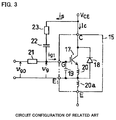
- Fig. 3 shows a circuit configuration proposed in Patent Document 1.
- an IGBT 17 and a diode 18 are connected parallel in reverse, and a collector terminal C, an emitter terminal E, a gate terminal G and a control emitter terminal E1 are provided.
- the IGBT 17 becomes ON or OFF on the basis of a gate voltage Vg applied across terminals G and E through a resistance 21, and a state between C-E terminals of the IGBT module 15 is brought into an ON state or an OFF state, thereby performing a switching operation.
- a reference sign 19 denotes a gate capacitance of the IGBT module 15, and reference signs 20 and 20a denote floating inductances (or stray inductances) appearing in a wiring inside the IGBT module 15.
- a resistance 23 and a capacitor 22, as the protection circuit, are connected in series between the collector terminal C and the gate terminal G of the IGBT 17.
- Patent Documents 3 and 4 have proposed a technique of applying a protection circuit in which an element having avalanche characteristics and a capacitor are combined.
- Patent Documents 5 and 6 have proposed a protection circuit in which an avalanche element, a resistance and a capacitor are combined.
- Fig. 4 shows a circuit configuration proposed in Patent Document 5.
- an inductive load L whose one end is connected to a DC voltage source +V is connected, at the other end thereof, to a drain Dr of a field-effect transistor T.
- a diode D whose polarity is as shown in the drawing, avalanche elements ZD3 ⁇ ZD10 whose polarities are opposite to that of the diode D and a resistance Rs are sequentially connected in series.
- a capacitor C1 is connected parallel to the avalanche element ZD3, and a resistance R3 and a capacitor C3 are connected in series between both ends of the avalanche element ZD5.
- a resistance R5 and a capacitor C5 are connected parallel between both ends of the avalanche element ZD7, and a resistance R8 is connected parallel to the avalanche element ZD10.
- Non-Patent Document 1 has disclosed a technique of protecting a switching element from overvoltage breakdown between a gate and an emitter of the switching element by connecting a Zener diode between the gate and the emitter of the switching element.
- Fig. 5 shows a circuit configuration disclosed in Non-Patent Document 1.
- a Zener diode 31 and a diode Ds whose polarity is as shown in the drawing are connected in series between a collector and a gate of an IGBT 50.
- a Zener diode 32 and a Zener diode 33 are connected in series with their polarities being opposite to each other between the gate and an emitter of the IGBT 50.
- a gate resistance R Goff and a drive voltage source 34 are connected in series between the gate and the emitter of the IGBT 50.
- Lk denotes an inductance.
- circuits of Figs. 4 and 5 it is possible to configure a circuit having both functions of overvoltage protection of a collector-emitter voltage of the switching element and overvoltage protection of a gate-emitter voltage of the switching element, as shown in Fig. 6 .
- a reference sign 50 denotes an IGBT as the switching element, which indicates one of a plurality of the IGBTs that are connected in series in a power conversion device .
- a reference sign 60 is a drive IC that outputs a gate command (a voltage of ON/OFF command) to a gate of the IGBT 50 through a gate resistance Rg.
- avalanche elements (avalanche diodes having avalanche characteristics) D1 ⁇ D5 whose polarities are as shown in the drawing and a resistance R4 are sequentially connected in series.
- a capacitor C1 and a resistance R1 are connected parallel between both ends of the avalanche element D4, and a capacitor C2 and a resistance R2 are connected parallel between both ends of the avalanche element D5.
- a Vce overvoltage protection circuit 41 is configured by these avalanche elements D1 ⁇ D5 , capacitors C1 and C2 and resistances R1, R2 and R4.
- a cathode of a Zener diode ZD11 is connected to a common connection point of the gate of the IGBT 50 and the resistance R4.
- An anode of the Zener diode ZD11 is connected to an emitter of the IGBT 50 through an anode and a cathode of a Zener diode ZD12.
- a Vge overvoltage protection circuit 42 is configured by these Zener diodes ZD11 and ZD12.
- Non-Patent Document 1 SEMIKRON Inc. HP, technical information, "IGBT and MOSFET power module” section 3.6.3.2 “overvoltage limit” Fig-3.61 (a), internet URL (http://www.semikron.com/skcompub/ja/application_man ual_2000-193.htm), October 24, 2013 Search
- FIG. 7 An example of a voltage waveform and a current waveform of each part in the circuit of Fig. 6 when the IGBT 50 is turned off is shown in Fig. 7 .
- I1 denotes a current that passes through the Vce overvoltage protection circuit 41
- I2 denotes a current that branches off from I1 and flows to the gate of the IGBT
- I3 denotes a current that branches off from I1 and passes through the Vge overvoltage protection circuit 42.
- a gate-emitter voltage Vge of the IGBT 50 decreases, and a collector-emitter voltage Vce increases .
- An object of the present invention is toprovide a protection circuit for a semiconductor switching element and a power conversion device which are capable of suppressing the variations in collector-emitter voltage between the semiconductor switching elements connected in series and capable of reducing the risk of breaking the semiconductor switching element due to the overvoltage breakdown and the thermal breakdown, upon turn-off of the semiconductor switching element.
- a protection circuit for a semiconductor switching element recited in claim 1 is a protection circuit provided for each of a plurality of semiconductor switching elements connected in series, comprising: a first protection circuit configured so that a cathode of a first avalanche element is connected to a collector of the semiconductor switching element, an anode of the first avalanche element is connected to a cathode of a second avalanche element, a first capacitor and a first resistance are connected parallel to the second avalanche element, and an anode of the second avalanche element is connected to one end of a second resistance; and a second protection circuit configured so that a cathode of a third avalanche element is connected to the other end of the second resistance, an anode of the third avalanche element is connected to an emitter of the semiconductor switching element, one end of a series component of third and fourth resistances is connected to a common connection point of the second resistance and the third avalanche element, and first and
- a power conversion device comprises: the protection circuit for the semiconductor switching element as claimed in any one of the preceding claims 1 to 4.
- a collector current can flow to a first protection circuit side by avalanche breakdown of the first and second avalanche elements.
- the second protection circuit suppresses variations in the collector-emitter voltage of each semiconductor switching element while suppressing overvoltage of a gate-emitter voltage of each semiconductor switching element.
- a second capacitor is connectedparallel to the third resistance or the fourth resistance of the second protection circuit.
- a plurality of first avalanche elements are connected in series.
- a plurality of parallel circuits each of which is configured by the second avalanche element, the first capacitor and the first resistance being connected parallel in the first protection circuit, are connected in series.
- Fig. 1 shows an embodiment in which the present invention is applied to a semiconductor switching element, which is one of semiconductor switching elements that are connected in series, in a power conversion device.
- a semiconductor switching element which is one of semiconductor switching elements that are connected in series, in a power conversion device.
- the same element etc. in Fig. 1 as those in Fig. 6 are denoted by the same reference signs.
- a reference sign 50 denotes an IGBT as the switching element, which indicates one of a plurality of IGBTs that are connected in series in the power conversion device.
- the IGBT is used as the semiconductor switching element, the semiconductor switching element is not limited to this IGBT, and other switching elements could be used.
- a reference sign 60 is a drive IC that outputs a gate command (a voltage Vge0 of ON/OFF command) to a gate of the IGBT 50 through a gate resistance Rg.
- a gate command a voltage Vge0 of ON/OFF command
- Vge0 +15V
- Vge0 -10V
- avalanche elements (avalanche diodes having avalanche characteristics) D1 ⁇ D5 whose cathodes are on a collector side of the IGBT 50, a resistance R4 and an avalanche element D6 whose cathode is on the collector side of the IGBT 50 are sequentially connected in series .
- a capacitor C1 and a resistance R1 are connected parallel between both ends of the avalanche element D4, and a capacitor C2 and a resistance R2 are connected parallel between both ends of the avalanche element D5.
- the number of avalanche elements D1 ⁇ D3 (a first avalanche element of the present invention) connected in series is determined by withstand voltage characteristics of each avalanche element and a circuit voltage. Although the number of avalanche elements connected in series is three in the present embodiment, it is not limited to three. The number of avalanche elements connected in series can be arbitrarily determined as long as it is one avalanche element or more.
- the resistances R1 and R2 are resistances for discharge of electric charge accumulated in the capacitors C1 and C2.
- the number of parallel circuits that are connected in series, each of which is configured by the capacitor (C1 ⁇ or C2 (a first capacitor of the present invention)), the avalanche element (D4 or D5 (a second avalanche element of the present invention)) and the resistance (R1 or R2 (a first resistance of the present invention)) being connected parallel, is determined by withstand voltage characteristics of each element and the circuit voltage. In the present embodiment, it is two series circuits. However, it is not limited to this, and the number of parallel circuits that are connected in series can be arbitrarily determined as long as it is one series circuit or more.
- a first protection circuit of the present invention is configured by these avalanche elements D1 ⁇ D5, capacitors C1 and C2 and resistances R1, R2 and R4.
- One end of a resistance R5 (a third resistance of the present invention) is connected to a common connection point of the resistance R4 (a second resistance of the present invention) and the avalanche element D6 (a third avalanche element of the present invention).
- the other end of the resistance R5 is connected to one end of a resistance R6 (a fourth resistance of the present invention).
- a capacitor C3 (a second capacitor of the present invention) is connected parallel to the resistance R6.
- the other end of the resistance R6 is connected to a cathode of a Zener diode ZD2 (a second Zener diode of the present invention) through an anode and a cathode of a Zener diode ZD1 (a first Zener diode of the present invention).
- An anode of the Zener diode ZD2 is connected to the gate of the IGBT 50.
- a second protection circuit of the present invention is configured by these resistances R5 and R6, capacitor C3, Zener diodes ZD1 and ZD2 and avalanche element D6.
- the Zener diodes ZD1 and ZD2 are used for suppressing a reverse current to an output of the drive IC 60 upon turn-on of the IGBT 50 and for decreasing applied voltages applied to the resistances R5 and R6 and the capacitor C3 . This decrease of the appliedvoltage brings about an effect of size reduction of the resistances R5 and R6 and the capacitor C3. Further, the Zener diodes ZD1 and ZD2 have the function of suppressing the overvoltage of a gate-emitter voltage Vge of the IGBT 50 together with the avalanche element D6.
- the resistance R4 has the function of restraining the current I1 .
- the resistances R5 andR6 and the capacitor C3 have the function of restraining the current I2.
- I1 denotes a current that passes through the avalanche elements D1 ⁇ D5, the capacitors C1 and C2 and the resistance R4.
- I2 denotes a current that branches off from I1 and flows to the gate of the IGBT 50 through the resistances R5 and R6, the capacitor C3 and the Zener diodes ZD1 and ZD2.
- I3 denotes a current that branches off from I1 and passes through the avalanche element D6.
- Vd1 When Vd1 reaches the avalanche voltage Vaval determined by the characteristics of the avalanche elements D1, D2 and D3 at time t2, the current I1 flows through the avalanche elements D1 ⁇ D3, the capacitors C1 and C2 and the resistance R4 by avalanche breakdown. Then, when an applied voltage (Vc1) of the capacitors C1 or C2 becomes a threshold value or greater during a time period t2-t3, the current I1 flows through the avalanche elements D4 and D5 connected parallel to the capacitors C1 and C2 respectively. With this, increase of the collector-emitter voltage Vce of the IGBT 50 is limited, and the overvoltage protection is performed.
- the current I2 flowing to the gate of the IGBT 50 flows so that a total voltage of (the applied voltage of the resistances R5 + the applied voltage of the resistances R6 + an applied voltage of the Zener diode ZD1 + an applied voltage of the Zener diode ZD2) balances with an applied voltage Vd2 of the avalanche element D6. With this, the gate-emitter voltage Vge of the IGBT 50 increases again.
- Vge of the IGBT 50 an impedance between the collector and the emitter of the IGBT 50 decreases, then balance of the collector-emitter voltage between the IGBTs connected in series is adjusted. Further, with this adjustment, variations in a collector-emitter voltage peak value Vcepeak between the IGBTs connected in series in the time period T4 are suppressed.
- the current I3 does not flow in the time period T4.
- each current I2 of the IGBTs connected in series is not affected by the current I3 .
- the present invention has the effect of further suppressing the variations in the collector-emitter voltage Vce of each IGBT connected in series in the time period T4.
- the present invention it is possible to suppress the variations in the collector-emitter voltage Vce of each switching element while suppressing the overvoltage of the gate-emitter voltage Vge upon turn-off of the switching element such as the IGBT connected in series. With this, (1) it is possible to reduce the risk of breaking the switching element due to the Vce overvoltage breakdown.
Landscapes
- Engineering & Computer Science (AREA)
- Power Engineering (AREA)
- Electronic Switches (AREA)
- Power Conversion In General (AREA)
Abstract
Description
- The present invention relates to a power conversion device using a voltage-driven switching element, and more particularly to a protection circuit for a semiconductor switching element and a power conversion device.
- There is a case where as a means to increase voltage of a power conversion device, a circuit configuration in which a plurality of semiconductor switching elements (e.g. IGBTs) are connected in series is applied. The switching element is brought into ON/OFF states by ON/OFF of a gate command inputted to a gate terminal of the switching element.
- When the gate commands of the switching elements connected in series are simultaneously changed to OFF, breakdown of the switching element might occur due to a difference of a gate command timing and/or a difference in voltage between the switching elements during a tail current period.
-
Patent Document 1 has proposed a technique of equalizing a collector-emitter voltage (a voltage between the collector and an emitter) of the switching element connected in series by applying, between a collector terminal and a gate terminal of the switching element, a protection circuit configured by a resistance and a capacitor.Fig. 3 shows a circuit configuration proposed inPatent Document 1. - In
Fig. 3 , in anIGBT module 15, anIGBT 17 and adiode 18 are connected parallel in reverse, and a collector terminal C, an emitter terminal E, a gate terminal G and a control emitter terminal E1 are provided. TheIGBT 17 becomes ON or OFF on the basis of a gate voltage Vg applied across terminals G and E through aresistance 21, and a state between C-E terminals of theIGBT module 15 is brought into an ON state or an OFF state, thereby performing a switching operation. Here, areference sign 19 denotes a gate capacitance of theIGBT module 15, andreference signs IGBT module 15. - A
resistance 23 and acapacitor 22, as the protection circuit, are connected in series between the collector terminal C and the gate terminal G of theIGBT 17. - Further, Patent Documents 3 and 4 have proposed a technique of applying a protection circuit in which an element having avalanche characteristics and a capacitor are combined. In addition, Patent Documents 5 and 6 have proposed a protection circuit in which an avalanche element, a resistance and a capacitor are combined.
-
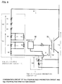
Fig. 4 shows a circuit configuration proposed in Patent Document 5. InFig. 4 , an inductive load L whose one end is connected to a DC voltage source +V is connected, at the other end thereof, to a drain Dr of a field-effect transistor T. Between the drain Dr and a gate G of the field-effect transistor T, a diode D whose polarity is as shown in the drawing, avalanche elements ZD3 ∼ ZD10 whose polarities are opposite to that of the diode D and a resistance Rs are sequentially connected in series. A capacitor C1 is connected parallel to the avalanche element ZD3, and a resistance R3 and a capacitor C3 are connected in series between both ends of the avalanche element ZD5. A resistance R5 and a capacitor C5 are connected parallel between both ends of the avalanche element ZD7, and a resistance R8 is connected parallel to the avalanche element ZD10. - Meanwhile, Non-Patent
Document 1 has disclosed a technique of protecting a switching element from overvoltage breakdown between a gate and an emitter of the switching element by connecting a Zener diode between the gate and the emitter of the switching element.Fig. 5 shows a circuit configuration disclosed in Non-PatentDocument 1. - In
Fig. 5 , a Zenerdiode 31 and a diode Ds whose polarity is as shown in the drawing are connected in series between a collector and a gate of anIGBT 50. A Zenerdiode 32 and a Zenerdiode 33 are connected in series with their polarities being opposite to each other between the gate and an emitter of theIGBT 50. Further, a gate resistance RGoff and adrive voltage source 34 are connected in series between the gate and the emitter of theIGBT 50. Lk denotes an inductance. - By combining circuits of
Figs. 4 and 5 , it is possible to configure a circuit having both functions of overvoltage protection of a collector-emitter voltage of the switching element and overvoltage protection of a gate-emitter voltage of the switching element, as shown inFig. 6 . - In
Fig. 6 , areference sign 50 denotes an IGBT as the switching element, which indicates one of a plurality of the IGBTs that are connected in series in a power conversion device . Areference sign 60 is a drive IC that outputs a gate command (a voltage of ON/OFF command) to a gate of theIGBT 50 through a gate resistance Rg. - Between a collector and a gate of the
IGBT 50, avalanche elements (avalanche diodes having avalanche characteristics) D1 ∼ D5 whose polarities are as shown in the drawing and a resistance R4 are sequentially connected in series. A capacitor C1 and a resistance R1 are connected parallel between both ends of the avalanche element D4, and a capacitor C2 and a resistance R2 are connected parallel between both ends of the avalanche element D5. A Vceovervoltage protection circuit 41 is configured by these avalanche elements D1 ~ D5 , capacitors C1 and C2 and resistances R1, R2 and R4. - A cathode of a Zener diode ZD11 is connected to a common connection point of the gate of the
IGBT 50 and the resistance R4. An anode of the Zener diode ZD11 is connected to an emitter of theIGBT 50 through an anode and a cathode of a Zener diode ZD12. A Vgeovervoltage protection circuit 42 is configured by these Zener diodes ZD11 and ZD12. -
- Patent Document 1: Japanese Patent Publication No.
3462032 - Patent Document 2: Japanese Patent Publication No.
3632385 - Patent Document 3: Japanese Patent PublicationNo.
3598933 - Patent Document 4: Japanese Patent Provisional Publication Tokkai No.
2010-124643 - Patent Document 5: German Patent Publication No.
DE19640433A1 - Patent Document 5: German Patent Publication No.
DE19740540C1 - Non-Patent Document 1: SEMIKRON Inc. HP, technical information, "IGBT and MOSFET power module" section 3.6.3.2 "overvoltage limit" Fig-3.61 (a), internet URL (http://www.semikron.com/skcompub/ja/application_man ual_2000-193.htm), October 24, 2013 Search
- An example of a voltage waveform and a current waveform of each part in the circuit of
Fig. 6 when theIGBT 50 is turned off is shown inFig. 7 . InFigs. 6 and7 , I1 denotes a current that passes through the Vceovervoltage protection circuit 41, I2 denotes a current that branches off from I1 and flows to the gate of the IGBT, and I3 denotes a current that branches off from I1 and passes through the Vgeovervoltage protection circuit 42. - First, when a voltage of an OFF command is outputted from the
drive IC 60 at time t1, a gate-emitter voltage Vge of the IGBT 50 (a voltage Vd2 of the Vge overvoltage protection circuit 42) decreases, and a collector-emitter voltage Vce increases . Then, when an applied voltage Vd1 of a series circuit of the avalanche elements D1 ∼ D3 reaches a threshold value Vaval that is determined by withstand voltage characteristics of the avalanche elements D1 ∼ D3 at time t2, the currents I1 and I2 flow through the avalanche elements D1 ∼ D3, the capacitors C1 and C2 and the resistance R4 by avalanche breakdown, and the gate-emitter voltage Vge of theIGBT 50 increases . With this, an impedance between the collector and the emitter of theIGBT 50 decreases, then balance of the collector-emitter voltage between the plurality of IGBTs connected in series is adjusted. - When an applied voltage (Vc1) of the capacitors C1 or C2 becomes a threshold value or greater during a time period t2-t3, the current I1 passing through the Vce
overvoltage protection circuit 41 flows through the avalanche elements D4 and D5 connected parallel to the capacitors C1 and C2 respectively. With this, increase of the collector-emitter voltage Vce of theIGBT 50 is limited, and the overvoltage protection is performed. - Next, from time t3 when the collector-emitter voltage Vce of the
IGBT 50 and the applied voltage Vd1 of the avalanche elements D1 ∼ D3 decrease and the currents I1 and I2 becomes zero, the voltage Vce and the voltage Vd1 increase again. - When the applied voltage Vd1 of the series circuit of the avalanche elements D1 ∼ D3 reaches the threshold value Vaval determined by the withstand voltage characteristics of the avalanche elements D1 ∼ D3 again at time t4, the currents I1 and I2 flow again.
- Here, the current I3 flowing through the Zener diodes ZD11 and ZD12 in the circuit of
Fig. 6 is a current that flows when the applied voltage Vd2 of the ZD11 and ZD12 becomes a threshold value VzD11 or greater by characteristics of the ZD11 and ZD12. Further, because of a relationship of "I2 = I1 - I3", when the I3 flows, I2 decreases. Furthermore, a value of this I3 is also affected by variations in characteristics of the Zener diodes ZD11 and ZD12. - Considering balance (equalization) of the collector-emitter voltage Vce between the IGBTs connected in series upon the turn-off of the IGBTs, "I2 = I1" is ideal. However, the fact that I3 flows by the characteristics of the ZD11 and ZD12 as described above causes variations in the current I2 of each IGBT connected in series. This causes variations in the collector-emitter voltage Vce of each
IGBT 50 in a time period (mainly, in a time period T4) when the currents I1 and I3 flow. Further, this also causes variations in a collector-emitter voltage peak value Vcepeak between the IGBTs connected in series in the time period T4. - The variations in Vce brings the following problems.
- (1) Vcepeak of one of the IGBTs connected in series exceeds an allowable voltage, and this entails risk that the IGBT will be broken due to Vce overvoltage breakdown.
- (2) Since the time period T4 is a time period in which switching loss of the IGBT connected in series increases, there is a possibility that thermal breakdown will occur due to increase of the switching loss of one of the IGBTs . In order to avoid this thermal breakdown, it is desirable to suppress the variations in Vce for the time period T4.
- The present invention was made to solve the above problems . An object of the present invention is toprovide a protection circuit for a semiconductor switching element and a power conversion device which are capable of suppressing the variations in collector-emitter voltage between the semiconductor switching elements connected in series and capable of reducing the risk of breaking the semiconductor switching element due to the overvoltage breakdown and the thermal breakdown, upon turn-off of the semiconductor switching element.
- In order to solve the above problems, a protection circuit for a semiconductor switching element recited in
claim 1 is a protection circuit provided for each of a plurality of semiconductor switching elements connected in series, comprising: a first protection circuit configured so that a cathode of a first avalanche element is connected to a collector of the semiconductor switching element, an anode of the first avalanche element is connected to a cathode of a second avalanche element, a first capacitor and a first resistance are connected parallel to the second avalanche element, and an anode of the second avalanche element is connected to one end of a second resistance; and a second protection circuit configured so that a cathode of a third avalanche element is connected to the other end of the second resistance, an anode of the third avalanche element is connected to an emitter of the semiconductor switching element, one end of a series component of third and fourth resistances is connected to a common connection point of the second resistance and the third avalanche element, and first and second Zener diodes are connected in series with their polarities being opposite to each other between the other end of the series component of third and fourth resistances and a gate of the semiconductor switching element. - Further, a power conversion device, recited in claim 5, comprises: the protection circuit for the semiconductor switching element as claimed in any one of the preceding
claims 1 to 4. - According to the above configuration, upon turn-off of the semiconductor switching element, when a collector-emitter voltage increases, a collector current can flow to a first protection circuit side by avalanche breakdown of the first and second avalanche elements. With this, the semiconductor switching element is protected from overvoltage breakdown. The second protection circuit suppresses variations in the collector-emitter voltage of each semiconductor switching element while suppressing overvoltage of a gate-emitter voltage of each semiconductor switching element.
- In the protection circuit for the semiconductor switching element recited in
claim 2, a second capacitor is connectedparallel to the third resistance or the fourth resistance of the second protection circuit. - According to the above configuration, since a differentiating circuit is configured by parallel connection of the third resistance or the fourth resistance and the second capacitor, a slope of the gate-emitter voltage of the semiconductor switching element becomes steep, and a transient response is improved. This brings about an effect of reduction of switching loss.
- In the protection circuit for the semiconductor switching element recited in claim 3 , a plurality of first avalanche elements are connected in series.
- In the protection circuit for the semiconductor switching element recited in claim 4, a plurality of parallel circuits, each of which is configured by the second avalanche element, the first capacitor and the first resistance being connected parallel in the first protection circuit, are connected in series.
- According to the above configuration, it is possible to design an optimum circuit according to withstand voltage characteristics of each avalanche element and a circuit voltage.
- (1) According to invention recited in
claims 1 to 5, it is possible to suppress the variations in collector-emitter voltage between the semiconductor switching elements connected in series and to reduce the risk of breaking the semiconductor switching element due to the overvoltage breakdown and the thermal breakdown, upon turn-off of the semiconductor switching element. - (2) According to invention recited in
claim 2, a slope of the gate-emitter voltage of the semiconductor switching element becomes steep, and a transient response is improved. This brings about an effect of reduction of switching loss. - (3) According to invention recited in claims 3 and 4, it is possible to design an optimum circuit according to withstand voltage characteristics of each avalanche element and a circuit voltage.
-
-
Fig. 1 is a circuit diagram of an embodiment of the present invention. -
Fig. 2 is a drawing of a voltage waveform and a current waveform of each part in the circuit ofFig. 1 . -
Fig. 3 is a circuit diagram showing an example of a related art protection circuit for a switching element. -
Fig. 4 is a circuit diagram showing other example of a related art protection circuit for a switching element. -
Fig. 5 is a circuit diagram showing other example of a related art protection circuit for a switching element. -
Fig. 6 is a configuration diagram of an overvoltage protection circuit configured by combining the circuits ofFigs. 4 and 5 . -
Fig. 7 is a drawing of a voltage waveform and a current waveform of each part in the circuit ofFig. 6 . - In the following description, embodiments of the present invention will be explained with reference to the drawings. The present invention is not limited to the following embodiments.
Fig. 1 shows an embodiment in which the present invention is applied to a semiconductor switching element, which is one of semiconductor switching elements that are connected in series, in a power conversion device. The same element etc. inFig. 1 as those inFig. 6 are denoted by the same reference signs. - In
Fig. 1 , areference sign 50 denotes an IGBT as the switching element, which indicates one of a plurality of IGBTs that are connected in series in the power conversion device. In the present embodiment, although the IGBT is used as the semiconductor switching element, the semiconductor switching element is not limited to this IGBT, and other switching elements could be used. - A
reference sign 60 is a drive IC that outputs a gate command (a voltage Vge0 of ON/OFF command) to a gate of theIGBT 50 through a gate resistance Rg. In the present embodiment, "Vge0 = +15V" is outputted at a time of an ON-command, and "Vge0 = -10V" is outputted at a time of an OFF-command. - Between a collector and an emitter of the
IGBT 50, avalanche elements (avalanche diodes having avalanche characteristics) D1 ∼ D5 whose cathodes are on a collector side of theIGBT 50, a resistance R4 and an avalanche element D6 whose cathode is on the collector side of theIGBT 50 are sequentially connected in series . A capacitor C1 and a resistance R1 are connected parallel between both ends of the avalanche element D4, and a capacitor C2 and a resistance R2 are connected parallel between both ends of the avalanche element D5. - The number of avalanche elements D1 ∼ D3 (a first avalanche element of the present invention) connected in series is determined by withstand voltage characteristics of each avalanche element and a circuit voltage. Although the number of avalanche elements connected in series is three in the present embodiment, it is not limited to three. The number of avalanche elements connected in series can be arbitrarily determined as long as it is one avalanche element or more.
- Upon turn-off of the
IGBT 50, when an applied voltage Vd1 of the avalanche elements D1 ∼ D3 exceeds an avalanche voltage Vaval that is determined by characteristics of the avalanche elements D1, D2 and D3, a current I1 flows through the capacitors C1 and C2, and the capacitors C1 and C2 are charged. The current I1 normally flows through the capacitors C1 and C2. However, when an applied voltage of the capacitors C1 or C2 becomes a threshold value or greater, the current I1 also flows through the avalanche elements D4 and D5 connected parallel to the capacitors C1 and C2 respectively. As a consequence, increase of a collector-emitter voltage Vce of theIGBT 50 is limited, and overvoltage protection of Vce is performed. - The resistances R1 and R2 are resistances for discharge of electric charge accumulated in the capacitors C1 and C2. The number of parallel circuits that are connected in series, each of which is configured by the capacitor (C1µ or C2 (a first capacitor of the present invention)), the avalanche element (D4 or D5 (a second avalanche element of the present invention)) and the resistance (R1 or R2 (a first resistance of the present invention)) being connected parallel, is determined by withstand voltage characteristics of each element and the circuit voltage. In the present embodiment, it is two series circuits. However, it is not limited to this, and the number of parallel circuits that are connected in series can be arbitrarily determined as long as it is one series circuit or more.
- A first protection circuit of the present invention is configured by these avalanche elements D1 ∼ D5, capacitors C1 and C2 and resistances R1, R2 and R4.
- One end of a resistance R5 (a third resistance of the present invention) is connected to a common connection point of the resistance R4 (a second resistance of the present invention) and the avalanche element D6 (a third avalanche element of the present invention).
- The other end of the resistance R5 is connected to one end of a resistance R6 (a fourth resistance of the present invention). A capacitor C3 (a second capacitor of the present invention) is connected parallel to the resistance R6.
- The other end of the resistance R6 is connected to a cathode of a Zener diode ZD2 (a second Zener diode of the present invention) through an anode and a cathode of a Zener diode ZD1 (a first Zener diode of the present invention). An anode of the Zener diode ZD2 is connected to the gate of the
IGBT 50. - A second protection circuit of the present invention is configured by these resistances R5 and R6, capacitor C3, Zener diodes ZD1 and ZD2 and avalanche element D6.
- The Zener diodes ZD1 and ZD2 are used for suppressing a reverse current to an output of the
drive IC 60 upon turn-on of theIGBT 50 and for decreasing applied voltages applied to the resistances R5 and R6 and the capacitor C3 . This decrease of the appliedvoltage brings about an effect of size reduction of the resistances R5 and R6 and the capacitor C3. Further, the Zener diodes ZD1 and ZD2 have the function of suppressing the overvoltage of a gate-emitter voltage Vge of theIGBT 50 together with the avalanche element D6. - The resistance R4 has the function of restraining the current I1 . The resistances R5 andR6 and the capacitor C3 have the function of restraining the current I2.
- Here, by using a differentiating circuit configured by the resistance R6 and the capacitor C3 being connected parallel, a slope of the gate-emitter voltage Vge of the
IGBT 50 becomes steep, and a transient response is improved. This brings about an effect of reduction of switching loss. - An example of a voltage waveform and a current waveform of each part in the circuit of
Fig. 1 when theIGBT 50 is turned off is shown inFig. 2 . InFigs. 1 and2 , I1 denotes a current that passes through the avalanche elements D1 ∼ D5, the capacitors C1 and C2 and the resistance R4. I2 denotes a current that branches off from I1 and flows to the gate of theIGBT 50 through the resistances R5 and R6, the capacitor C3 and the Zener diodes ZD1 and ZD2. I3 denotes a current that branches off from I1 and passes through the avalanche element D6. - Next, operation in each time period in
Fig. 2 will be explained below. - First, when an output signal of the
drive IC 60 becomes the OFF-command and "Vge0 = -10V" is outputted at time t1, the gate-emitter voltage Vge of theIGBT 50 decreases, and theIGBT 50 is turned off. The collector-emitter voltage Vce then increases at a certain slope. With increase of the collector-emitter voltage Vce, the applied voltage Vd1 of the series circuit of the avalanche elements D1, D2 and D3 also increases. - When Vd1 reaches the avalanche voltage Vaval determined by the characteristics of the avalanche elements D1, D2 and D3 at time t2, the current I1 flows through the avalanche elements D1 ∼ D3, the capacitors C1 and C2 and the resistance R4 by avalanche breakdown. Then, when an applied voltage (Vc1) of the capacitors C1 or C2 becomes a threshold value or greater during a time period t2-t3, the current I1 flows through the avalanche elements D4 and D5 connected parallel to the capacitors C1 and C2 respectively. With this, increase of the collector-emitter voltage Vce of the
IGBT 50 is limited, and the overvoltage protection is performed. - The current I2 flowing to the gate of the
IGBT 50 flows so that a total voltage of (the applied voltage of the resistances R5 + the applied voltage of the resistances R6 + an applied voltage of the Zener diode ZD1 + an applied voltage of the Zener diode ZD2) balances with an applied voltage Vd2 of the avalanche element D6. With this, the gate-emitter voltage Vge of theIGBT 50 increases again. - When the applied voltage Vd2 reaches an avalanche voltage Vava2 that is determined by characteristics of the avalanche element D6, the current I3 flows through the avalanche element D6. Increase of the current I2 is then restrained, and I2 shortly decreases. When the gate-emitter voltage Vge of the
IGBT 50 increases to a predetermined voltage, by a relationship of a potential difference between Vd2 and Vge, I2 becomes 0 (I2 = 0), and I1 becomes 0 (I1 = 0). Because of "I1 = 0", I3 becomes 0 (I3 = 0) (at time t3). - The gate-emitter voltage Vge of the
IGBT 50, which has increased by the operation for the time period T2, gradually decreases from time t3 by a discharge operation of thedrive IC 60 outputting "Vge0 = -10V". Meanwhile, the collector-emitter voltage Vce of theIGBT 50 that is in turn-off increases by and with decrease of Vge. With this increase of Vce, the applied voltage Vd1 of the avalanche elements D1 ∼ D3 also increases. - When the applied voltage Vd1 reaches the avalanche voltage Vaval again at time t4, the current I1 flows again. Since a magnitude of the current I1 at this time is smaller than that in the time period T2, the applied voltage Vd2 of the avalanche element D6 does not reach the avalanche voltage Vava2 of the avalanche element D6 , and the current does not flow to the avalanche element D6, namely "I3 = 0".
- Therefore, the current of "I2 = I1" flows, and the gate-emitter voltage Vge of the
IGBT 50 increases. By the increase of the gate-emitter voltage Vge of theIGBT 50 , an impedance between the collector and the emitter of theIGBT 50 decreases, then balance of the collector-emitter voltage between the IGBTs connected in series is adjusted. Further, with this adjustment, variations in a collector-emitter voltage peak value Vcepeak between the IGBTs connected in series in the time period T4 are suppressed. - As explained above, in the present invention, the current I3 does not flow in the time period T4. Thus, each current I2 of the IGBTs connected in series is not affected by the current I3 . Accordingly, as compared with a related art circuit of
Fig. 6 in which the current I3 flows in the time period T4, variations in the current I2 are suppressed, then the present invention has the effect of further suppressing the variations in the collector-emitter voltage Vce of each IGBT connected in series in the time period T4. - According to the present invention, it is possible to suppress the variations in the collector-emitter voltage Vce of each switching element while suppressing the overvoltage of the gate-emitter voltage Vge upon turn-off of the switching element such as the IGBT connected in series. With this, (1) it is possible to reduce the risk of breaking the switching element due to the Vce overvoltage breakdown.
- (2) It is possible to suppress imbalance of switching loss of the switching element connected in series and to reduce the risk of breaking the semiconductor switching element due to the thermal breakdown.
Claims (5)
- A protection circuit provided for each of a plurality of semiconductor switching elements connected in series, comprising:a first protection circuit configured so that a cathode of a first avalanche element is connected to a collector of the semiconductor switching element, an anode of the first avalanche element is connected to a cathode of a second avalanche element, a first capacitor and a first resistance are connected parallel to the second avalanche element, and an anode of the second avalanche element is connected to one end of a second resistance; anda second protection circuit configured so that a cathode of a third avalanche element is connected to the other end of the second resistance, an anode of the third avalanche element is connected to an emitter of the semiconductor switching element, one end of a series component of third and fourth resistances is connected to a common connection point of the second resistance and the third avalanche element, and first and second Zener diodes are connected in series with their polarities being opposite to each other between the other end of the series component of third and fourth resistances and a gate of the semiconductor switching element.
- The protection circuit for the semiconductor switching element, as claimed in claim 1, wherein:a second capacitor is connectedparallel to the third resistance or the fourth resistance of the second protection circuit.
- The protection circuit for the semiconductor switching element, as claimed in claim 1 or 2, wherein:a plurality of first avalanche elements are connected in series.
- The protection circuit for the semiconductor switching element, as claimed in claim 1 or 2 or 3, wherein:a plurality of parallel circuits, each of which is configured by the second avalanche element, the first capacitor and the first resistance being connectedparallel in the first protection circuit, are connected in series.
- A power conversion device comprising:the protection circuit for the semiconductor switching element as claimed in any one of the preceding claims 1 to 4.
Applications Claiming Priority (2)
| Application Number | Priority Date | Filing Date | Title |
|---|---|---|---|
| JP2013231641A JP6156073B2 (en) | 2013-11-08 | 2013-11-08 | Semiconductor switching element protection circuit and power conversion device |
| PCT/JP2014/079410 WO2015068755A1 (en) | 2013-11-08 | 2014-11-06 | Protection circuit for semiconductor switching element, and power conversion device |
Publications (3)
| Publication Number | Publication Date |
|---|---|
| EP3068051A1 true EP3068051A1 (en) | 2016-09-14 |
| EP3068051A4 EP3068051A4 (en) | 2017-06-28 |
| EP3068051B1 EP3068051B1 (en) | 2019-08-07 |
Family
ID=53041532
Family Applications (1)
| Application Number | Title | Priority Date | Filing Date |
|---|---|---|---|
| EP14860798.9A Not-in-force EP3068051B1 (en) | 2013-11-08 | 2014-11-06 | Protection circuit for semiconductor switching element, and power conversion device |
Country Status (6)
| Country | Link |
|---|---|
| US (1) | US10014763B2 (en) |
| EP (1) | EP3068051B1 (en) |
| JP (1) | JP6156073B2 (en) |
| BR (1) | BR112016010471B1 (en) |
| RU (1) | RU2641479C2 (en) |
| WO (1) | WO2015068755A1 (en) |
Cited By (1)
| Publication number | Priority date | Publication date | Assignee | Title |
|---|---|---|---|---|
| EP3461006A3 (en) * | 2017-09-20 | 2019-06-26 | Nuctech Company Limited | Protection circuit, oscillation compensation circuit and power supply circuit in solid state pulse modulator |
Families Citing this family (4)
| Publication number | Priority date | Publication date | Assignee | Title |
|---|---|---|---|---|
| CN109075781B (en) * | 2017-03-30 | 2020-01-21 | 三菱电机株式会社 | Driving circuit of power semiconductor element and motor driving device |
| JP6985600B2 (en) * | 2018-01-25 | 2021-12-22 | 富士通株式会社 | Waveform forming circuit, semiconductor device and switching power supply device |
| CN113889994B (en) * | 2021-10-09 | 2024-04-12 | 富芯微电子有限公司 | IGBT overvoltage protection device |
| WO2024180008A1 (en) * | 2023-02-28 | 2024-09-06 | Siemens Aktiengesellschaft | Electronic interruption unit |
Family Cites Families (16)
| Publication number | Priority date | Publication date | Assignee | Title |
|---|---|---|---|---|
| DE19640433C2 (en) * | 1996-09-30 | 2000-10-12 | Siemens Ag | Power output stage for switching inductive consumers |
| JP3462032B2 (en) | 1997-03-04 | 2003-11-05 | 株式会社東芝 | Power converter |
| FI107662B (en) | 1997-06-10 | 2001-09-14 | Lexel Finland Ab Oy | Transient |
| JP3632385B2 (en) | 1997-07-30 | 2005-03-23 | 株式会社デンソー | Inductive load drive circuit |
| DE19740540C1 (en) | 1997-09-15 | 1999-03-18 | Siemens Ag | Circuit arrangement for limiting overvoltages in power semiconductors |
| US5920224A (en) * | 1998-02-17 | 1999-07-06 | Harris Corporation | Network for improving electro-magnetic interference response |
| JP3255147B2 (en) * | 1998-06-19 | 2002-02-12 | 株式会社デンソー | Surge protection circuit for insulated gate transistor |
| JP3598933B2 (en) | 2000-02-28 | 2004-12-08 | 株式会社日立製作所 | Power converter |
| JP2003023769A (en) * | 2001-07-06 | 2003-01-24 | Sansha Electric Mfg Co Ltd | Power semiconductor module |
| FR2832000B1 (en) * | 2001-11-05 | 2006-07-21 | Alstom | DEVICE FOR PROTECTION AGAINST OVERVOLTAGES OF A POWER COMPONENT |
| JP2008042950A (en) | 2006-08-01 | 2008-02-21 | Mitsubishi Electric Corp | Power converter |
| JP5309923B2 (en) | 2008-11-21 | 2013-10-09 | 富士電機株式会社 | Semiconductor device drive circuit |
| US8283896B1 (en) * | 2009-06-03 | 2012-10-09 | Polarity, Inc. | Method and system for charging and discharging high-voltage energy storage devices |
| US9030855B2 (en) * | 2011-07-14 | 2015-05-12 | Macronix International Co., Ltd. | Semiconductor device, start-up circuit having first and second circuits and a single voltage output terminal coupled to a second node between the semiconductor unit and the first circuit, and operating method for the same |
| JP5682587B2 (en) * | 2012-03-28 | 2015-03-11 | 株式会社デンソー | Semiconductor device |
| US8780516B2 (en) * | 2012-05-08 | 2014-07-15 | General Electric Conpany | Systems, methods, and apparatus for voltage clamp circuits |
-
2013
- 2013-11-08 JP JP2013231641A patent/JP6156073B2/en active Active
-
2014
- 2014-11-06 BR BR112016010471-4A patent/BR112016010471B1/en active IP Right Grant
- 2014-11-06 WO PCT/JP2014/079410 patent/WO2015068755A1/en not_active Ceased
- 2014-11-06 US US15/034,952 patent/US10014763B2/en not_active Expired - Fee Related
- 2014-11-06 EP EP14860798.9A patent/EP3068051B1/en not_active Not-in-force
- 2014-11-06 RU RU2016119940A patent/RU2641479C2/en active
Cited By (2)
| Publication number | Priority date | Publication date | Assignee | Title |
|---|---|---|---|---|
| EP3461006A3 (en) * | 2017-09-20 | 2019-06-26 | Nuctech Company Limited | Protection circuit, oscillation compensation circuit and power supply circuit in solid state pulse modulator |
| US11152932B2 (en) | 2017-09-20 | 2021-10-19 | Nuctech Company Limited | Protection circuit, oscillation compensation circuit and power supply circuit in solid state pulse modulator |
Also Published As
| Publication number | Publication date |
|---|---|
| JP6156073B2 (en) | 2017-07-05 |
| RU2641479C2 (en) | 2018-01-17 |
| US20160276921A1 (en) | 2016-09-22 |
| BR112016010471A2 (en) | 2017-08-08 |
| WO2015068755A1 (en) | 2015-05-14 |
| BR112016010471B1 (en) | 2022-02-08 |
| JP2015092790A (en) | 2015-05-14 |
| US10014763B2 (en) | 2018-07-03 |
| EP3068051A4 (en) | 2017-06-28 |
| EP3068051B1 (en) | 2019-08-07 |
| RU2016119940A (en) | 2017-12-13 |
Similar Documents
| Publication | Publication Date | Title |
|---|---|---|
| US20230327661A1 (en) | Cascode switches including normally-off and normally-on devices and circuits comprising the switches | |
| CN107980199B (en) | Power supply switch device | |
| US8362812B2 (en) | Switching gate driver | |
| US8928363B2 (en) | Semiconductor drive circuit and power conversion apparatus using same | |
| CN104604134B (en) | Semiconductor device | |
| US8513983B2 (en) | Gate drive circuit with overdrive protection | |
| US10187049B2 (en) | Driving device and inductive load driving device | |
| EP2549650A1 (en) | Method for driving IGBT | |
| EP3068051B1 (en) | Protection circuit for semiconductor switching element, and power conversion device | |
| US20120235710A1 (en) | Circuit Arrangement with a MOSFET and an IGBT | |
| KR20130060143A (en) | Semiconductor switch and power conversion device | |
| EP3787164A1 (en) | Gate drive circuit and gate drive method | |
| US9059697B2 (en) | Drive circuit and drive method for driving normally-on-type transistor | |
| JP2015185618A (en) | Semiconductor device | |
| JP5254386B2 (en) | Gate drive circuit and power semiconductor module | |
| JPWO2015111154A1 (en) | Switching circuit, inverter circuit, and motor control device | |
| JPWO2016030933A1 (en) | Power converter | |
| US12334917B2 (en) | Voltage-source gate drive having shunt capacitors and shunt resistors | |
| KR20190011494A (en) | GATE DRIVING CIRCUIT FOR SiC MOSFET | |
| WO2016143023A1 (en) | Gate drive circuit, inverter circuit, and motor control device | |
| JP5563050B2 (en) | Gate drive circuit and power semiconductor module | |
| JP6312946B1 (en) | Power semiconductor element drive circuit and motor drive device | |
| US20250141338A1 (en) | Gate drive circuit and power conversion device using same | |
| JP2023160795A (en) | How power transistor circuits work |
Legal Events
| Date | Code | Title | Description |
|---|---|---|---|
| PUAI | Public reference made under article 153(3) epc to a published international application that has entered the european phase |
Free format text: ORIGINAL CODE: 0009012 |
|
| 17P | Request for examination filed |
Effective date: 20160523 |
|
| AK | Designated contracting states |
Kind code of ref document: A1 Designated state(s): AL AT BE BG CH CY CZ DE DK EE ES FI FR GB GR HR HU IE IS IT LI LT LU LV MC MK MT NL NO PL PT RO RS SE SI SK SM TR |
|
| AX | Request for extension of the european patent |
Extension state: BA ME |
|
| DAX | Request for extension of the european patent (deleted) | ||
| A4 | Supplementary search report drawn up and despatched |
Effective date: 20170531 |
|
| RIC1 | Information provided on ipc code assigned before grant |
Ipc: H03K 17/10 20060101ALI20170524BHEP Ipc: H03K 17/082 20060101ALI20170524BHEP Ipc: H03K 17/16 20060101AFI20170524BHEP Ipc: H02M 1/00 20070101ALI20170524BHEP Ipc: H03K 17/08 20060101ALI20170524BHEP |
|
| GRAP | Despatch of communication of intention to grant a patent |
Free format text: ORIGINAL CODE: EPIDOSNIGR1 |
|
| STAA | Information on the status of an ep patent application or granted ep patent |
Free format text: STATUS: GRANT OF PATENT IS INTENDED |
|
| INTG | Intention to grant announced |
Effective date: 20181129 |
|
| GRAJ | Information related to disapproval of communication of intention to grant by the applicant or resumption of examination proceedings by the epo deleted |
Free format text: ORIGINAL CODE: EPIDOSDIGR1 |
|
| STAA | Information on the status of an ep patent application or granted ep patent |
Free format text: STATUS: REQUEST FOR EXAMINATION WAS MADE |
|
| GRAP | Despatch of communication of intention to grant a patent |
Free format text: ORIGINAL CODE: EPIDOSNIGR1 |
|
| STAA | Information on the status of an ep patent application or granted ep patent |
Free format text: STATUS: GRANT OF PATENT IS INTENDED |
|
| INTC | Intention to grant announced (deleted) | ||
| INTG | Intention to grant announced |
Effective date: 20190215 |
|
| GRAS | Grant fee paid |
Free format text: ORIGINAL CODE: EPIDOSNIGR3 |
|
| GRAA | (expected) grant |
Free format text: ORIGINAL CODE: 0009210 |
|
| STAA | Information on the status of an ep patent application or granted ep patent |
Free format text: STATUS: THE PATENT HAS BEEN GRANTED |
|
| AK | Designated contracting states |
Kind code of ref document: B1 Designated state(s): AL AT BE BG CH CY CZ DE DK EE ES FI FR GB GR HR HU IE IS IT LI LT LU LV MC MK MT NL NO PL PT RO RS SE SI SK SM TR |
|
| REG | Reference to a national code |
Ref country code: GB Ref legal event code: FG4D |
|
| REG | Reference to a national code |
Ref country code: CH Ref legal event code: EP Ref country code: AT Ref legal event code: REF Ref document number: 1165377 Country of ref document: AT Kind code of ref document: T Effective date: 20190815 |
|
| REG | Reference to a national code |
Ref country code: DE Ref legal event code: R096 Ref document number: 602014051523 Country of ref document: DE |
|
| REG | Reference to a national code |
Ref country code: IE Ref legal event code: FG4D |
|
| REG | Reference to a national code |
Ref country code: NL Ref legal event code: MP Effective date: 20190807 |
|
| REG | Reference to a national code |
Ref country code: LT Ref legal event code: MG4D |
|
| PG25 | Lapsed in a contracting state [announced via postgrant information from national office to epo] |
Ref country code: FI Free format text: LAPSE BECAUSE OF FAILURE TO SUBMIT A TRANSLATION OF THE DESCRIPTION OR TO PAY THE FEE WITHIN THE PRESCRIBED TIME-LIMIT Effective date: 20190807 Ref country code: NO Free format text: LAPSE BECAUSE OF FAILURE TO SUBMIT A TRANSLATION OF THE DESCRIPTION OR TO PAY THE FEE WITHIN THE PRESCRIBED TIME-LIMIT Effective date: 20191107 Ref country code: HR Free format text: LAPSE BECAUSE OF FAILURE TO SUBMIT A TRANSLATION OF THE DESCRIPTION OR TO PAY THE FEE WITHIN THE PRESCRIBED TIME-LIMIT Effective date: 20190807 Ref country code: LT Free format text: LAPSE BECAUSE OF FAILURE TO SUBMIT A TRANSLATION OF THE DESCRIPTION OR TO PAY THE FEE WITHIN THE PRESCRIBED TIME-LIMIT Effective date: 20190807 Ref country code: BG Free format text: LAPSE BECAUSE OF FAILURE TO SUBMIT A TRANSLATION OF THE DESCRIPTION OR TO PAY THE FEE WITHIN THE PRESCRIBED TIME-LIMIT Effective date: 20191107 Ref country code: SE Free format text: LAPSE BECAUSE OF FAILURE TO SUBMIT A TRANSLATION OF THE DESCRIPTION OR TO PAY THE FEE WITHIN THE PRESCRIBED TIME-LIMIT Effective date: 20190807 Ref country code: NL Free format text: LAPSE BECAUSE OF FAILURE TO SUBMIT A TRANSLATION OF THE DESCRIPTION OR TO PAY THE FEE WITHIN THE PRESCRIBED TIME-LIMIT Effective date: 20190807 Ref country code: PT Free format text: LAPSE BECAUSE OF FAILURE TO SUBMIT A TRANSLATION OF THE DESCRIPTION OR TO PAY THE FEE WITHIN THE PRESCRIBED TIME-LIMIT Effective date: 20191209 |
|
| REG | Reference to a national code |
Ref country code: AT Ref legal event code: MK05 Ref document number: 1165377 Country of ref document: AT Kind code of ref document: T Effective date: 20190807 |
|
| PG25 | Lapsed in a contracting state [announced via postgrant information from national office to epo] |
Ref country code: AL Free format text: LAPSE BECAUSE OF FAILURE TO SUBMIT A TRANSLATION OF THE DESCRIPTION OR TO PAY THE FEE WITHIN THE PRESCRIBED TIME-LIMIT Effective date: 20190807 Ref country code: GR Free format text: LAPSE BECAUSE OF FAILURE TO SUBMIT A TRANSLATION OF THE DESCRIPTION OR TO PAY THE FEE WITHIN THE PRESCRIBED TIME-LIMIT Effective date: 20191108 Ref country code: RS Free format text: LAPSE BECAUSE OF FAILURE TO SUBMIT A TRANSLATION OF THE DESCRIPTION OR TO PAY THE FEE WITHIN THE PRESCRIBED TIME-LIMIT Effective date: 20190807 Ref country code: IS Free format text: LAPSE BECAUSE OF FAILURE TO SUBMIT A TRANSLATION OF THE DESCRIPTION OR TO PAY THE FEE WITHIN THE PRESCRIBED TIME-LIMIT Effective date: 20191207 Ref country code: LV Free format text: LAPSE BECAUSE OF FAILURE TO SUBMIT A TRANSLATION OF THE DESCRIPTION OR TO PAY THE FEE WITHIN THE PRESCRIBED TIME-LIMIT Effective date: 20190807 Ref country code: ES Free format text: LAPSE BECAUSE OF FAILURE TO SUBMIT A TRANSLATION OF THE DESCRIPTION OR TO PAY THE FEE WITHIN THE PRESCRIBED TIME-LIMIT Effective date: 20190807 |
|
| PG25 | Lapsed in a contracting state [announced via postgrant information from national office to epo] |
Ref country code: TR Free format text: LAPSE BECAUSE OF FAILURE TO SUBMIT A TRANSLATION OF THE DESCRIPTION OR TO PAY THE FEE WITHIN THE PRESCRIBED TIME-LIMIT Effective date: 20190807 |
|
| PG25 | Lapsed in a contracting state [announced via postgrant information from national office to epo] |
Ref country code: IT Free format text: LAPSE BECAUSE OF FAILURE TO SUBMIT A TRANSLATION OF THE DESCRIPTION OR TO PAY THE FEE WITHIN THE PRESCRIBED TIME-LIMIT Effective date: 20190807 Ref country code: AT Free format text: LAPSE BECAUSE OF FAILURE TO SUBMIT A TRANSLATION OF THE DESCRIPTION OR TO PAY THE FEE WITHIN THE PRESCRIBED TIME-LIMIT Effective date: 20190807 Ref country code: DK Free format text: LAPSE BECAUSE OF FAILURE TO SUBMIT A TRANSLATION OF THE DESCRIPTION OR TO PAY THE FEE WITHIN THE PRESCRIBED TIME-LIMIT Effective date: 20190807 Ref country code: PL Free format text: LAPSE BECAUSE OF FAILURE TO SUBMIT A TRANSLATION OF THE DESCRIPTION OR TO PAY THE FEE WITHIN THE PRESCRIBED TIME-LIMIT Effective date: 20190807 Ref country code: EE Free format text: LAPSE BECAUSE OF FAILURE TO SUBMIT A TRANSLATION OF THE DESCRIPTION OR TO PAY THE FEE WITHIN THE PRESCRIBED TIME-LIMIT Effective date: 20190807 Ref country code: RO Free format text: LAPSE BECAUSE OF FAILURE TO SUBMIT A TRANSLATION OF THE DESCRIPTION OR TO PAY THE FEE WITHIN THE PRESCRIBED TIME-LIMIT Effective date: 20190807 |
|
| PG25 | Lapsed in a contracting state [announced via postgrant information from national office to epo] |
Ref country code: CZ Free format text: LAPSE BECAUSE OF FAILURE TO SUBMIT A TRANSLATION OF THE DESCRIPTION OR TO PAY THE FEE WITHIN THE PRESCRIBED TIME-LIMIT Effective date: 20190807 Ref country code: SM Free format text: LAPSE BECAUSE OF FAILURE TO SUBMIT A TRANSLATION OF THE DESCRIPTION OR TO PAY THE FEE WITHIN THE PRESCRIBED TIME-LIMIT Effective date: 20190807 Ref country code: IS Free format text: LAPSE BECAUSE OF FAILURE TO SUBMIT A TRANSLATION OF THE DESCRIPTION OR TO PAY THE FEE WITHIN THE PRESCRIBED TIME-LIMIT Effective date: 20200224 Ref country code: SK Free format text: LAPSE BECAUSE OF FAILURE TO SUBMIT A TRANSLATION OF THE DESCRIPTION OR TO PAY THE FEE WITHIN THE PRESCRIBED TIME-LIMIT Effective date: 20190807 |
|
| REG | Reference to a national code |
Ref country code: DE Ref legal event code: R097 Ref document number: 602014051523 Country of ref document: DE |
|
| PLBE | No opposition filed within time limit |
Free format text: ORIGINAL CODE: 0009261 |
|
| STAA | Information on the status of an ep patent application or granted ep patent |
Free format text: STATUS: NO OPPOSITION FILED WITHIN TIME LIMIT |
|
| PG2D | Information on lapse in contracting state deleted |
Ref country code: IS |
|
| PG25 | Lapsed in a contracting state [announced via postgrant information from national office to epo] |
Ref country code: LU Free format text: LAPSE BECAUSE OF NON-PAYMENT OF DUE FEES Effective date: 20191106 Ref country code: MC Free format text: LAPSE BECAUSE OF FAILURE TO SUBMIT A TRANSLATION OF THE DESCRIPTION OR TO PAY THE FEE WITHIN THE PRESCRIBED TIME-LIMIT Effective date: 20190807 |
|
| 26N | No opposition filed |
Effective date: 20200603 |
|
| REG | Reference to a national code |
Ref country code: BE Ref legal event code: MM Effective date: 20191130 |
|
| PG25 | Lapsed in a contracting state [announced via postgrant information from national office to epo] |
Ref country code: SI Free format text: LAPSE BECAUSE OF FAILURE TO SUBMIT A TRANSLATION OF THE DESCRIPTION OR TO PAY THE FEE WITHIN THE PRESCRIBED TIME-LIMIT Effective date: 20190807 |
|
| GBPC | Gb: european patent ceased through non-payment of renewal fee |
Effective date: 20191107 |
|
| PG25 | Lapsed in a contracting state [announced via postgrant information from national office to epo] |
Ref country code: GB Free format text: LAPSE BECAUSE OF NON-PAYMENT OF DUE FEES Effective date: 20191107 Ref country code: IE Free format text: LAPSE BECAUSE OF NON-PAYMENT OF DUE FEES Effective date: 20191106 |
|
| PG25 | Lapsed in a contracting state [announced via postgrant information from national office to epo] |
Ref country code: BE Free format text: LAPSE BECAUSE OF NON-PAYMENT OF DUE FEES Effective date: 20191130 |
|
| PGFP | Annual fee paid to national office [announced via postgrant information from national office to epo] |
Ref country code: FR Payment date: 20201120 Year of fee payment: 7 Ref country code: DE Payment date: 20201119 Year of fee payment: 7 Ref country code: CH Payment date: 20201118 Year of fee payment: 7 |
|
| PG25 | Lapsed in a contracting state [announced via postgrant information from national office to epo] |
Ref country code: CY Free format text: LAPSE BECAUSE OF FAILURE TO SUBMIT A TRANSLATION OF THE DESCRIPTION OR TO PAY THE FEE WITHIN THE PRESCRIBED TIME-LIMIT Effective date: 20190807 |
|
| PG25 | Lapsed in a contracting state [announced via postgrant information from national office to epo] |
Ref country code: MT Free format text: LAPSE BECAUSE OF FAILURE TO SUBMIT A TRANSLATION OF THE DESCRIPTION OR TO PAY THE FEE WITHIN THE PRESCRIBED TIME-LIMIT Effective date: 20190807 Ref country code: HU Free format text: LAPSE BECAUSE OF FAILURE TO SUBMIT A TRANSLATION OF THE DESCRIPTION OR TO PAY THE FEE WITHIN THE PRESCRIBED TIME-LIMIT; INVALID AB INITIO Effective date: 20141106 |
|
| REG | Reference to a national code |
Ref country code: DE Ref legal event code: R119 Ref document number: 602014051523 Country of ref document: DE |
|
| PG25 | Lapsed in a contracting state [announced via postgrant information from national office to epo] |
Ref country code: MK Free format text: LAPSE BECAUSE OF FAILURE TO SUBMIT A TRANSLATION OF THE DESCRIPTION OR TO PAY THE FEE WITHIN THE PRESCRIBED TIME-LIMIT Effective date: 20190807 |
|
| REG | Reference to a national code |
Ref country code: CH Ref legal event code: PL |
|
| PG25 | Lapsed in a contracting state [announced via postgrant information from national office to epo] |
Ref country code: DE Free format text: LAPSE BECAUSE OF NON-PAYMENT OF DUE FEES Effective date: 20220601 |
|
| PG25 | Lapsed in a contracting state [announced via postgrant information from national office to epo] |
Ref country code: FR Free format text: LAPSE BECAUSE OF NON-PAYMENT OF DUE FEES Effective date: 20211130 |
|
| PG25 | Lapsed in a contracting state [announced via postgrant information from national office to epo] |
Ref country code: LI Free format text: LAPSE BECAUSE OF NON-PAYMENT OF DUE FEES Effective date: 20220630 Ref country code: CH Free format text: LAPSE BECAUSE OF NON-PAYMENT OF DUE FEES Effective date: 20220630 |