EP3067924A1 - Composite solder ball, semiconductor package using the same, semiconductor device using the same and manufacturing method thereof - Google Patents
Composite solder ball, semiconductor package using the same, semiconductor device using the same and manufacturing method thereof Download PDFInfo
- Publication number
- EP3067924A1 EP3067924A1 EP15193187.0A EP15193187A EP3067924A1 EP 3067924 A1 EP3067924 A1 EP 3067924A1 EP 15193187 A EP15193187 A EP 15193187A EP 3067924 A1 EP3067924 A1 EP 3067924A1
- Authority
- EP
- European Patent Office
- Prior art keywords
- substrate
- core
- composite solder
- semiconductor package
- solder ball
- Prior art date
- Legal status (The legal status is an assumption and is not a legal conclusion. Google has not performed a legal analysis and makes no representation as to the accuracy of the status listed.)
- Granted
Links
Images



Classifications
-
- B—PERFORMING OPERATIONS; TRANSPORTING
- B23—MACHINE TOOLS; METAL-WORKING NOT OTHERWISE PROVIDED FOR
- B23K—SOLDERING OR UNSOLDERING; WELDING; CLADDING OR PLATING BY SOLDERING OR WELDING; CUTTING BY APPLYING HEAT LOCALLY, e.g. FLAME CUTTING; WORKING BY LASER BEAM
- B23K35/00—Rods, electrodes, materials, or media, for use in soldering, welding, or cutting
- B23K35/02—Rods, electrodes, materials, or media, for use in soldering, welding, or cutting characterised by mechanical features, e.g. shape
- B23K35/0222—Rods, electrodes, materials, or media, for use in soldering, welding, or cutting characterised by mechanical features, e.g. shape for use in soldering or brazing
- B23K35/0244—Powders, particles or spheres; Preforms made therefrom
-
- B—PERFORMING OPERATIONS; TRANSPORTING
- B23—MACHINE TOOLS; METAL-WORKING NOT OTHERWISE PROVIDED FOR
- B23K—SOLDERING OR UNSOLDERING; WELDING; CLADDING OR PLATING BY SOLDERING OR WELDING; CUTTING BY APPLYING HEAT LOCALLY, e.g. FLAME CUTTING; WORKING BY LASER BEAM
- B23K35/00—Rods, electrodes, materials, or media, for use in soldering, welding, or cutting
- B23K35/22—Rods, electrodes, materials, or media, for use in soldering, welding, or cutting characterised by the composition or nature of the material
- B23K35/24—Selection of soldering or welding materials proper
- B23K35/26—Selection of soldering or welding materials proper with the principal constituent melting at less than 400°C
-
- B—PERFORMING OPERATIONS; TRANSPORTING
- B23—MACHINE TOOLS; METAL-WORKING NOT OTHERWISE PROVIDED FOR
- B23K—SOLDERING OR UNSOLDERING; WELDING; CLADDING OR PLATING BY SOLDERING OR WELDING; CUTTING BY APPLYING HEAT LOCALLY, e.g. FLAME CUTTING; WORKING BY LASER BEAM
- B23K35/00—Rods, electrodes, materials, or media, for use in soldering, welding, or cutting
- B23K35/22—Rods, electrodes, materials, or media, for use in soldering, welding, or cutting characterised by the composition or nature of the material
- B23K35/24—Selection of soldering or welding materials proper
- B23K35/26—Selection of soldering or welding materials proper with the principal constituent melting at less than 400°C
- B23K35/262—Sn as the principal constituent
-
- B—PERFORMING OPERATIONS; TRANSPORTING
- B23—MACHINE TOOLS; METAL-WORKING NOT OTHERWISE PROVIDED FOR
- B23K—SOLDERING OR UNSOLDERING; WELDING; CLADDING OR PLATING BY SOLDERING OR WELDING; CUTTING BY APPLYING HEAT LOCALLY, e.g. FLAME CUTTING; WORKING BY LASER BEAM
- B23K35/00—Rods, electrodes, materials, or media, for use in soldering, welding, or cutting
- B23K35/22—Rods, electrodes, materials, or media, for use in soldering, welding, or cutting characterised by the composition or nature of the material
- B23K35/24—Selection of soldering or welding materials proper
- B23K35/26—Selection of soldering or welding materials proper with the principal constituent melting at less than 400°C
- B23K35/264—Bi as the principal constituent
-
- B—PERFORMING OPERATIONS; TRANSPORTING
- B23—MACHINE TOOLS; METAL-WORKING NOT OTHERWISE PROVIDED FOR
- B23K—SOLDERING OR UNSOLDERING; WELDING; CLADDING OR PLATING BY SOLDERING OR WELDING; CUTTING BY APPLYING HEAT LOCALLY, e.g. FLAME CUTTING; WORKING BY LASER BEAM
- B23K35/00—Rods, electrodes, materials, or media, for use in soldering, welding, or cutting
- B23K35/22—Rods, electrodes, materials, or media, for use in soldering, welding, or cutting characterised by the composition or nature of the material
- B23K35/24—Selection of soldering or welding materials proper
- B23K35/30—Selection of soldering or welding materials proper with the principal constituent melting at less than 1550°C
-
- H—ELECTRICITY
- H10—SEMICONDUCTOR DEVICES; ELECTRIC SOLID-STATE DEVICES NOT OTHERWISE PROVIDED FOR
- H10W—GENERIC PACKAGES, INTERCONNECTIONS, CONNECTORS OR OTHER CONSTRUCTIONAL DETAILS OF DEVICES COVERED BY CLASS H10
- H10W70/00—Package substrates; Interposers; Redistribution layers [RDL]
- H10W70/60—Insulating or insulated package substrates; Interposers; Redistribution layers
- H10W70/62—Insulating or insulated package substrates; Interposers; Redistribution layers characterised by their interconnections
- H10W70/65—Shapes or dispositions of interconnections
-
- H—ELECTRICITY
- H10—SEMICONDUCTOR DEVICES; ELECTRIC SOLID-STATE DEVICES NOT OTHERWISE PROVIDED FOR
- H10W—GENERIC PACKAGES, INTERCONNECTIONS, CONNECTORS OR OTHER CONSTRUCTIONAL DETAILS OF DEVICES COVERED BY CLASS H10
- H10W70/00—Package substrates; Interposers; Redistribution layers [RDL]
- H10W70/60—Insulating or insulated package substrates; Interposers; Redistribution layers
- H10W70/62—Insulating or insulated package substrates; Interposers; Redistribution layers characterised by their interconnections
- H10W70/66—Conductive materials thereof
-
- H—ELECTRICITY
- H10—SEMICONDUCTOR DEVICES; ELECTRIC SOLID-STATE DEVICES NOT OTHERWISE PROVIDED FOR
- H10W—GENERIC PACKAGES, INTERCONNECTIONS, CONNECTORS OR OTHER CONSTRUCTIONAL DETAILS OF DEVICES COVERED BY CLASS H10
- H10W70/00—Package substrates; Interposers; Redistribution layers [RDL]
- H10W70/60—Insulating or insulated package substrates; Interposers; Redistribution layers
- H10W70/67—Insulating or insulated package substrates; Interposers; Redistribution layers characterised by their insulating layers or insulating parts
- H10W70/69—Insulating materials thereof
-
- H—ELECTRICITY
- H10—SEMICONDUCTOR DEVICES; ELECTRIC SOLID-STATE DEVICES NOT OTHERWISE PROVIDED FOR
- H10W—GENERIC PACKAGES, INTERCONNECTIONS, CONNECTORS OR OTHER CONSTRUCTIONAL DETAILS OF DEVICES COVERED BY CLASS H10
- H10W90/00—Package configurations
-
- H—ELECTRICITY
- H10—SEMICONDUCTOR DEVICES; ELECTRIC SOLID-STATE DEVICES NOT OTHERWISE PROVIDED FOR
- H10W—GENERIC PACKAGES, INTERCONNECTIONS, CONNECTORS OR OTHER CONSTRUCTIONAL DETAILS OF DEVICES COVERED BY CLASS H10
- H10W90/00—Package configurations
- H10W90/701—Package configurations characterised by the relative positions of pads or connectors relative to package parts
-
- B—PERFORMING OPERATIONS; TRANSPORTING
- B23—MACHINE TOOLS; METAL-WORKING NOT OTHERWISE PROVIDED FOR
- B23K—SOLDERING OR UNSOLDERING; WELDING; CLADDING OR PLATING BY SOLDERING OR WELDING; CUTTING BY APPLYING HEAT LOCALLY, e.g. FLAME CUTTING; WORKING BY LASER BEAM
- B23K2101/00—Articles made by soldering, welding or cutting
- B23K2101/36—Electric or electronic devices
- B23K2101/40—Semiconductor devices
-
- H—ELECTRICITY
- H10—SEMICONDUCTOR DEVICES; ELECTRIC SOLID-STATE DEVICES NOT OTHERWISE PROVIDED FOR
- H10W—GENERIC PACKAGES, INTERCONNECTIONS, CONNECTORS OR OTHER CONSTRUCTIONAL DETAILS OF DEVICES COVERED BY CLASS H10
- H10W70/00—Package substrates; Interposers; Redistribution layers [RDL]
- H10W70/60—Insulating or insulated package substrates; Interposers; Redistribution layers
-
- H—ELECTRICITY
- H10—SEMICONDUCTOR DEVICES; ELECTRIC SOLID-STATE DEVICES NOT OTHERWISE PROVIDED FOR
- H10W—GENERIC PACKAGES, INTERCONNECTIONS, CONNECTORS OR OTHER CONSTRUCTIONAL DETAILS OF DEVICES COVERED BY CLASS H10
- H10W72/00—Interconnections or connectors in packages
- H10W72/071—Connecting or disconnecting
- H10W72/072—Connecting or disconnecting of bump connectors
- H10W72/07231—Techniques
- H10W72/07236—Soldering or alloying
-
- H—ELECTRICITY
- H10—SEMICONDUCTOR DEVICES; ELECTRIC SOLID-STATE DEVICES NOT OTHERWISE PROVIDED FOR
- H10W—GENERIC PACKAGES, INTERCONNECTIONS, CONNECTORS OR OTHER CONSTRUCTIONAL DETAILS OF DEVICES COVERED BY CLASS H10
- H10W72/00—Interconnections or connectors in packages
- H10W72/20—Bump connectors, e.g. solder bumps or copper pillars; Dummy bumps; Thermal bumps
- H10W72/221—Structures or relative sizes
- H10W72/222—Multilayered bumps, e.g. a coating on top and side surfaces of a bump core
- H10W72/223—Multilayered bumps, e.g. a coating on top and side surfaces of a bump core characterised by the structure of the outermost layers, e.g. multilayered coatings
-
- H—ELECTRICITY
- H10—SEMICONDUCTOR DEVICES; ELECTRIC SOLID-STATE DEVICES NOT OTHERWISE PROVIDED FOR
- H10W—GENERIC PACKAGES, INTERCONNECTIONS, CONNECTORS OR OTHER CONSTRUCTIONAL DETAILS OF DEVICES COVERED BY CLASS H10
- H10W72/00—Interconnections or connectors in packages
- H10W72/20—Bump connectors, e.g. solder bumps or copper pillars; Dummy bumps; Thermal bumps
- H10W72/231—Shapes
- H10W72/232—Plan-view shape, i.e. in top view
-
- H—ELECTRICITY
- H10—SEMICONDUCTOR DEVICES; ELECTRIC SOLID-STATE DEVICES NOT OTHERWISE PROVIDED FOR
- H10W—GENERIC PACKAGES, INTERCONNECTIONS, CONNECTORS OR OTHER CONSTRUCTIONAL DETAILS OF DEVICES COVERED BY CLASS H10
- H10W72/00—Interconnections or connectors in packages
- H10W72/20—Bump connectors, e.g. solder bumps or copper pillars; Dummy bumps; Thermal bumps
- H10W72/241—Dispositions, e.g. layouts
- H10W72/245—Dispositions, e.g. layouts of outermost layers of multilayered bumps, e.g. bump coating being only on a part of a bump core
-
- H—ELECTRICITY
- H10—SEMICONDUCTOR DEVICES; ELECTRIC SOLID-STATE DEVICES NOT OTHERWISE PROVIDED FOR
- H10W—GENERIC PACKAGES, INTERCONNECTIONS, CONNECTORS OR OTHER CONSTRUCTIONAL DETAILS OF DEVICES COVERED BY CLASS H10
- H10W72/00—Interconnections or connectors in packages
- H10W72/20—Bump connectors, e.g. solder bumps or copper pillars; Dummy bumps; Thermal bumps
- H10W72/251—Materials
- H10W72/252—Materials comprising solid metals or solid metalloids, e.g. PbSn, Ag or Cu
-
- H—ELECTRICITY
- H10—SEMICONDUCTOR DEVICES; ELECTRIC SOLID-STATE DEVICES NOT OTHERWISE PROVIDED FOR
- H10W—GENERIC PACKAGES, INTERCONNECTIONS, CONNECTORS OR OTHER CONSTRUCTIONAL DETAILS OF DEVICES COVERED BY CLASS H10
- H10W72/00—Interconnections or connectors in packages
- H10W72/20—Bump connectors, e.g. solder bumps or copper pillars; Dummy bumps; Thermal bumps
- H10W72/251—Materials
- H10W72/255—Materials of outermost layers of multilayered bumps, e.g. material of a coating
-
- H—ELECTRICITY
- H10—SEMICONDUCTOR DEVICES; ELECTRIC SOLID-STATE DEVICES NOT OTHERWISE PROVIDED FOR
- H10W—GENERIC PACKAGES, INTERCONNECTIONS, CONNECTORS OR OTHER CONSTRUCTIONAL DETAILS OF DEVICES COVERED BY CLASS H10
- H10W74/00—Encapsulations, e.g. protective coatings
- H10W74/10—Encapsulations, e.g. protective coatings characterised by their shape or disposition
- H10W74/15—Encapsulations, e.g. protective coatings characterised by their shape or disposition on active surfaces of flip-chip devices, e.g. underfills
-
- H—ELECTRICITY
- H10—SEMICONDUCTOR DEVICES; ELECTRIC SOLID-STATE DEVICES NOT OTHERWISE PROVIDED FOR
- H10W—GENERIC PACKAGES, INTERCONNECTIONS, CONNECTORS OR OTHER CONSTRUCTIONAL DETAILS OF DEVICES COVERED BY CLASS H10
- H10W90/00—Package configurations
- H10W90/401—Package configurations characterised by multiple insulating or insulated package substrates, interposers or RDLs
-
- H—ELECTRICITY
- H10—SEMICONDUCTOR DEVICES; ELECTRIC SOLID-STATE DEVICES NOT OTHERWISE PROVIDED FOR
- H10W—GENERIC PACKAGES, INTERCONNECTIONS, CONNECTORS OR OTHER CONSTRUCTIONAL DETAILS OF DEVICES COVERED BY CLASS H10
- H10W90/00—Package configurations
- H10W90/701—Package configurations characterised by the relative positions of pads or connectors relative to package parts
- H10W90/721—Package configurations characterised by the relative positions of pads or connectors relative to package parts of bump connectors
- H10W90/722—Package configurations characterised by the relative positions of pads or connectors relative to package parts of bump connectors between stacked chips
-
- H—ELECTRICITY
- H10—SEMICONDUCTOR DEVICES; ELECTRIC SOLID-STATE DEVICES NOT OTHERWISE PROVIDED FOR
- H10W—GENERIC PACKAGES, INTERCONNECTIONS, CONNECTORS OR OTHER CONSTRUCTIONAL DETAILS OF DEVICES COVERED BY CLASS H10
- H10W90/00—Package configurations
- H10W90/701—Package configurations characterised by the relative positions of pads or connectors relative to package parts
- H10W90/721—Package configurations characterised by the relative positions of pads or connectors relative to package parts of bump connectors
- H10W90/724—Package configurations characterised by the relative positions of pads or connectors relative to package parts of bump connectors between a chip and a stacked insulating package substrate, interposer or RDL
-
- H—ELECTRICITY
- H10—SEMICONDUCTOR DEVICES; ELECTRIC SOLID-STATE DEVICES NOT OTHERWISE PROVIDED FOR
- H10W—GENERIC PACKAGES, INTERCONNECTIONS, CONNECTORS OR OTHER CONSTRUCTIONAL DETAILS OF DEVICES COVERED BY CLASS H10
- H10W90/00—Package configurations
- H10W90/701—Package configurations characterised by the relative positions of pads or connectors relative to package parts
- H10W90/731—Package configurations characterised by the relative positions of pads or connectors relative to package parts of die-attach connectors
- H10W90/734—Package configurations characterised by the relative positions of pads or connectors relative to package parts of die-attach connectors between a chip and a stacked insulating package substrate, interposer or RDL
Definitions
- the invention relates to a solder ball, a semiconductor package using the same, a semiconductor device using the same and a manufacturing method thereof, and more particularly to a composite solder ball, a semiconductor package using the same, a semiconductor device using the same and a manufacturing method thereof.
- PoP Package-on-package
- a composite solder ball in one embodiment, includes a core, an encapsulating layer and a barrier layer.
- the barrier layer is disposed between the core and the encapsulating layer. Wherein a melting point of the barrier layer is higher than a melting point of the core, the melting point of the core is higher than a melting point of the encapsulating layer.
- a semiconductor package in another embodiment, includes a first substrate, a second substrate, a composite solder ball and a first semiconductor component.
- the composite solder ball includes a core, an encapsulating layer and a barrier layer.
- the composite solder ball is disposed between the first substrate and the second substrate for electrically connecting the first substrate and the second substrate.
- the barrier layer is disposed between the core and the encapsulating layer. Wherein a melting point of the barrier layer is higher than a melting point of the core, the melting point of the core is higher than a melting point of the encapsulating layer.
- the first semiconductor component is disposed between the first substrate and the second substrate.
- a semiconductor device in another embodiment, includes a semiconductor package and a second semiconductor component.
- the second semiconductor component is disposed on the second substrate of the semiconductor package.
- the semiconductor package includes a first substrate, a second substrate, a composite solder ball and a first semiconductor component.
- the composite solder ball includes a core, an encapsulating layer and a barrier layer.
- the composite solder ball is disposed between the first substrate and the second substrate for electrically connecting the first substrate and the second substrate.
- the barrier layer is disposed between the core and the encapsulating layer. Wherein a melting point of the barrier layer is higher than a melting point of the core, the melting point of the core is higher than a melting point of the encapsulating layer.
- the first semiconductor component is disposed between the first substrate and the second substrate.
- a manufacturing method of a semiconductor package includes the following steps.
- a first substrate is provided; a first semiconductor component is disposed on the first substrate; a second substrate is provided; a plurality of composite solder balls are disposed on the second substrate; the first substrate is connected to the second substrate by way of the composite solder balls facing the first substrate, wherein the composite solder balls are disposed between the first substrate and the second substrate.
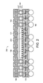
- FIG. 1 illustrates a diagram of a semiconductor package 100 according to an embodiment of the invention.
- the semiconductor package 100 includes a first substrate 110, a second substrate 120, a first semiconductor component 130, a plurality composite solder balls 140, a package body 150 and a plurality of conductive contacts 160.
- the first substrate 110 is, for example, a multi-layered coreless substrate.
- the first substrate 110 includes a plurality of pads 111 for electrically connected to the composite solder balls 140.
- the second substrate 120 is, for example, an interposer.
- the first semiconductor component 130 may be disposed on and electrically connected to the first substrate 110 through the composite solder balls 140.
- the second substrate 120 may be electrically connected to the first semiconductor component 130 through the composite solder balls 140 and the second substrate 120.
- the first semiconductor component 130 is coupled to an upper surface 110u of the first substrate 110 in a "face-down” orientation and electrically connected to the first substrate 110 via a plurality of conductive contacts 131.
- This configuration is sometimes referred to as "flip-chip".
- the conductive contact 131 may be solder ball, conductive pillar, etc.
- the first semiconductor component 130 may be coupled to the first substrate 110 in a "face-up" orientation, and electrically connected to the first substrate 110 via a plurality of conductive bond wires (not shown).
- the first semiconductor component 130 may be an active chip or a passive component, such as a resistor, an inductor or a capacitor. In another embodiment, the number of the first semiconductor component 130 may be several.
- Each composite solder ball 140 includes a core 141, a barrier layer 142 and an encapsulating layer 143.
- the barrier layer 142 is disposed between the core 141 and the encapsulating layer 143.
- the barrier layer 142 directly or indirectly encapsulates the core 141
- the encapsulating layer 143 directly or indirectly encapsulates the barrier layer 142.
- the melting point of the core 141 may be higher than the melting point of the encapsulating layer 143, such that the core 141 may be prevented from melting and deforming during reflow process, Therefore, it is possible to prevent an outer diameter D1 of the core 141 from expanding, and accordingly the minimum interval P1 between adjacent two composite solder balls 140 do not be narrowed, such that adjacent two composite solder balls 140 may be prevented from being electrically short to each other, and the density of the composite solder balls 140 may be increased.
- the core 141 may be made of a material including tin, bismuth or a combination thereof. In another embodiment, the core 141 may be made of a material in absence of copper. As a result, the outer diameter D1 of the core 141 may be reduced, such that the outer diameter D2 of the encapsulating layer 143 encapsulating the core 141 may be reduced and/or the thickness of the semiconductor package 100 may be reduced. In one embodiment, after reflow, the encapsulating layer 143 has the outer diameter D2 ranging between 120 ⁇ m and 130 ⁇ m.
- the melting point of the barrier layer 142 may be higher than the melting point of the core 141, such that the barrier layer 142 can restrict the outer diameter D1 of the core 141 and accordingly can prevent the core 141 from over-deforming during reflow process.
- the core 141 may be made a material having hardness and/or strength lower than that of the barrier layer 142.
- the barrier layer 142 may be made of a material including nickel whose hardness and/or strength is larger than the core 141.
- the encapsulating layer 143 may be pre-solder. Under such design, the semiconductor package 100 may omit extra pre-solder which is pre-applied on the first substrate 110 and/or the second substrate 120.
- the encapsulating layer 143 may be made of an alloy material including at least two of tin, silver and copper.
- the package body 150 is formed between the first substrate 110 and the second substrate 120 and encapsulates the first semiconductor component 130 and the composite solder balls 140.
- the package body 150 can include, for example, a Novolac-based resin, an epoxy-based resin, a silicone-based resin, or another suitable encapsulant. Suitable fillers also can be included, such as powdered SiO2.
- the conductive contacts 160 are disposed on a bottom surface 110b of the first substrate 110.
- the semiconductor package 100 is disposed on and electrically connected to an exterior circuit, such as a circuit board.
- the conductive contact 160 may be solder ball, conductive pillar, etc.
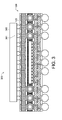
- FIG. 2 illustrates a diagram of a semiconductor package 200 according to another embodiment of the invention.
- the semiconductor package 200 includes the first substrate 110, the second substrate 120, the first semiconductor component 130, the composite solder balls 140, an under fill 250 and a plurality of conductive contacts 160.
- the under fill 250 is formed between the first semiconductor component 130 and the first substrate 110 and encapsulates a plurality of conductive contacts 131 of the first semiconductor component 130.
- the semiconductor package 200 omits the package body 150.
- the semiconductor package 200 may further includes the package body 150 encapsulating the first semiconductor component 130, the composite solder balls 140 and the under fill 250.
- FIG. 3 illustrates a diagram of a semiconductor device 300 according to another embodiment of the invention.
- the semiconductor device 300 includes a semiconductor package 100 and a second semiconductor component 360.
- the second semiconductor component 360 may be, for example, a memory, a semiconductor component rather than memory, another semiconductor package, active component, passive component, etc.
- the second semiconductor component 360 is disposed on and electrically connected to the second substrate 120 of the semiconductor package 100 through a plurality of conductive contacts 361.
- the conductive contact 361 may be solder ball, pillar, etc.
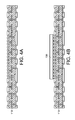
- FIGS. 4A to 4F illustrate manufacturing processes of the semiconductor package 100 of FIG. 1 .
- the first substrate 110 is provided.
- the first semiconductor component 130 is disposed on the first substrate 110 using, for example, surface mount technology (SMT).
- SMT surface mount technology
- the second substrate 120 is provided.
- a plurality of composite solder balls 140 are disposed on the second substrate 120 using, for example, ball mounting technology.
- Each composite solder ball 140 includes the core 141, the barrier layer 142 and the encapsulating layer 143.
- the barrier layer 142 is disposed between the core 141 and the encapsulating layer 143.
- the barrier layer 142 directly or indirectly encapsulates the core 141
- the encapsulating layer 143 directly or indirectly encapsulates the barrier layer 142.
- the first substrate 110 is connected to the second substrate 120 by way of the composite solder balls 140 facing the first substrate 110, wherein the composite solder balls 140 are disposed between the first substrate 110 and the second substrate 120 for electrically connecting the first substrate 110 and the second substrate 120.
- the encapsulating layer 143 of the composite solder balls 140 is melted to solder with the pads 111 of the first substrate 110. Since the melting point of the core 141 is higher than the melting point of the encapsulating layer 143, the reflowing temperature may be sufficiently high. For example, the reflowing temperature may reach 245°C or higher, such that the encapsulating layer 143 can firm formed on the pads 111 of the first substrate 110, and the core 141 may be prevented from melting and/or over-deforming. In another embodiment, the reflowing temperature may approach or exceed the melting point of the core 141.
- the melting point of the barrier layer 142 is higher than the melting point of the core 141, such that, during reflow process, the barrier layer 142 can restrict the outer diameter D1 of the core 141 and accordingly can prevent the core 141 from over-deforming.
- the package body 150 is disposed over the upper surface 110u of the first substrate 110 and encapsulates the first semiconductor component 130.
- the package body 150 can be formed by various packaging technologies, such as, for example, compression molding, injection molding, transfer molding or dispensing technology.
- the conductive contacts 160 of FIG. 1 may be disposed on the bottom surface of 110b of the first substrate 110 of IFG. 1 so as to form the semiconductor package 100 as illustrated in FIG. 1 .
- FIG. 5 illustrates a manufacturing process of the semiconductor package 200 of FIG. 2 .
- the under fill 250 is formed between the first substrate 110 and the first semiconductor component 130 and encapsulates the conductive contacts 131 using, for example, dispensing technology.
- the other formation steps of the semiconductor package 200 are similar to the corresponding steps of the semiconductor package 100 of FIG. 1 , and the similarities are not repeated here.
Landscapes
- Engineering & Computer Science (AREA)
- Mechanical Engineering (AREA)
- Wire Bonding (AREA)
Abstract
Description
- The invention relates to a solder ball, a semiconductor package using the same, a semiconductor device using the same and a manufacturing method thereof, and more particularly to a composite solder ball, a semiconductor package using the same, a semiconductor device using the same and a manufacturing method thereof.
- In the electronics industry, high integration and multiple functions with high performance become essential for new products. And meanwhile, high integration may cause higher manufacturing cost, since the manufacturing cost is in proportional to its size. Therefore, demanding on miniaturization of integrated circuit (IC) packages has become more and more critical.
- Package-on-package (PoP) is now the fastest growing semiconductor package technology since it is a cost-effective solution to high-density system integration in a single package. In a PoP structure, various packages are integrated in a single semiconductor package to reduce the size. Accordingly, there exists a need to provide a semiconductor package to overcomes, or at least reduces the above-mentioned problems.
- Therefore, it is important to increase the performance of the 3D graphic processing circuit while reducing the consumption of the electric power and extending the operating time of the mobile device.
- In one embodiment of the invention, a composite solder ball is provided. The composite solder ball includes a core, an encapsulating layer and a barrier layer. The barrier layer is disposed between the core and the encapsulating layer. Wherein a melting point of the barrier layer is higher than a melting point of the core, the melting point of the core is higher than a melting point of the encapsulating layer.
- In another embodiment of the invention, a semiconductor package is provided. The semiconductor package includes a first substrate, a second substrate, a composite solder ball and a first semiconductor component. The composite solder ball includes a core, an encapsulating layer and a barrier layer. The composite solder ball is disposed between the first substrate and the second substrate for electrically connecting the first substrate and the second substrate. The barrier layer is disposed between the core and the encapsulating layer. Wherein a melting point of the barrier layer is higher than a melting point of the core, the melting point of the core is higher than a melting point of the encapsulating layer. The first semiconductor component is disposed between the first substrate and the second substrate.
- In another embodiment of the invention, a semiconductor device is provided. The semiconductor device includes a semiconductor package and a second semiconductor component. The second semiconductor component is disposed on the second substrate of the semiconductor package. The semiconductor package includes a first substrate, a second substrate, a composite solder ball and a first semiconductor component. The composite solder ball includes a core, an encapsulating layer and a barrier layer. The composite solder ball is disposed between the first substrate and the second substrate for electrically connecting the first substrate and the second substrate. The barrier layer is disposed between the core and the encapsulating layer. Wherein a melting point of the barrier layer is higher than a melting point of the core, the melting point of the core is higher than a melting point of the encapsulating layer. The first semiconductor component is disposed between the first substrate and the second substrate.
- In another embodiment of the invention, a manufacturing method of a semiconductor package is provided. The manufacturing method includes the following steps. A first substrate is provided; a first semiconductor component is disposed on the first substrate; a second substrate is provided; a plurality of composite solder balls are disposed on the second substrate; the first substrate is connected to the second substrate by way of the composite solder balls facing the first substrate, wherein the composite solder balls are disposed between the first substrate and the second substrate.
- Numerous objects, features and advantages of the invention will be readily apparent upon a reading of the following detailed description of embodiments of the invention when taken in conjunction with the accompanying drawings. However, the drawings employed herein are for the purpose of descriptions and should not be regarded as limiting.
- The above objects and advantages of the invention will become more readily apparent to those ordinarily skilled in the art after reviewing the following detailed description and accompanying drawings, in which:
-
FIG. 1 illustrates a diagram of a semiconductor package according to an embodiment of the invention; -
FIG. 2 illustrates a diagram of a semiconductor package according to another embodiment of the invention; -
FIG. 3 illustrates a diagram of a semiconductor device according to another embodiment of the invention; -
FIGS 4A to 4F illustrate manufacturing processes of the semiconductor package ofFIG. 1 ; and -
FIG. 5 illustrates a manufacturing process of the semiconductor package ofFIG. 2 . -
FIG. 1 illustrates a diagram of asemiconductor package 100 according to an embodiment of the invention. Thesemiconductor package 100 includes afirst substrate 110, asecond substrate 120, afirst semiconductor component 130, a pluralitycomposite solder balls 140, apackage body 150 and a plurality ofconductive contacts 160. - The
first substrate 110 is, for example, a multi-layered coreless substrate. Thefirst substrate 110 includes a plurality ofpads 111 for electrically connected to thecomposite solder balls 140. Thesecond substrate 120 is, for example, an interposer. - The
first semiconductor component 130 may be disposed on and electrically connected to thefirst substrate 110 through thecomposite solder balls 140. Thesecond substrate 120 may be electrically connected to thefirst semiconductor component 130 through thecomposite solder balls 140 and thesecond substrate 120. - In the present embodiment, the
first semiconductor component 130 is coupled to anupper surface 110u of thefirst substrate 110 in a "face-down" orientation and electrically connected to thefirst substrate 110 via a plurality ofconductive contacts 131. This configuration is sometimes referred to as "flip-chip". Theconductive contact 131 may be solder ball, conductive pillar, etc. - In other embodiments, the
first semiconductor component 130 may be coupled to thefirst substrate 110 in a "face-up" orientation, and electrically connected to thefirst substrate 110 via a plurality of conductive bond wires (not shown). Thefirst semiconductor component 130 may be an active chip or a passive component, such as a resistor, an inductor or a capacitor. In another embodiment, the number of thefirst semiconductor component 130 may be several. - Each
composite solder ball 140 includes acore 141, abarrier layer 142 and an encapsulatinglayer 143. Thebarrier layer 142 is disposed between thecore 141 and theencapsulating layer 143. For example, thebarrier layer 142 directly or indirectly encapsulates thecore 141, and theencapsulating layer 143 directly or indirectly encapsulates thebarrier layer 142. - The melting point of the
core 141 may be higher than the melting point of theencapsulating layer 143, such that thecore 141 may be prevented from melting and deforming during reflow process, Therefore, it is possible to prevent an outer diameter D1 of thecore 141 from expanding, and accordingly the minimum interval P1 between adjacent twocomposite solder balls 140 do not be narrowed, such that adjacent twocomposite solder balls 140 may be prevented from being electrically short to each other, and the density of thecomposite solder balls 140 may be increased. - In one embodiment, the
core 141 may be made of a material including tin, bismuth or a combination thereof. In another embodiment, thecore 141 may be made of a material in absence of copper. As a result, the outer diameter D1 of thecore 141 may be reduced, such that the outer diameter D2 of theencapsulating layer 143 encapsulating thecore 141 may be reduced and/or the thickness of thesemiconductor package 100 may be reduced. In one embodiment, after reflow, the encapsulatinglayer 143 has the outer diameter D2 ranging between 120 µm and 130 µm. - In addition, the melting point of the
barrier layer 142 may be higher than the melting point of thecore 141, such that thebarrier layer 142 can restrict the outer diameter D1 of thecore 141 and accordingly can prevent the core 141 from over-deforming during reflow process. Furthermore, since thebarrier layer 142 can restrict the outer diameter D1 of thecore 141, thecore 141 may be made a material having hardness and/or strength lower than that of thebarrier layer 142. For example, thebarrier layer 142 may be made of a material including nickel whose hardness and/or strength is larger than thecore 141. - In addition, the
encapsulating layer 143 may be pre-solder. Under such design, thesemiconductor package 100 may omit extra pre-solder which is pre-applied on thefirst substrate 110 and/or thesecond substrate 120. In one embodiment, theencapsulating layer 143 may be made of an alloy material including at least two of tin, silver and copper. - The
package body 150 is formed between thefirst substrate 110 and thesecond substrate 120 and encapsulates thefirst semiconductor component 130 and thecomposite solder balls 140. - The
package body 150 can include, for example, a Novolac-based resin, an epoxy-based resin, a silicone-based resin, or another suitable encapsulant. Suitable fillers also can be included, such as powdered SiO2. - The
conductive contacts 160 are disposed on abottom surface 110b of thefirst substrate 110. Thesemiconductor package 100 is disposed on and electrically connected to an exterior circuit, such as a circuit board. Theconductive contact 160 may be solder ball, conductive pillar, etc. -
FIG. 2 illustrates a diagram of asemiconductor package 200 according to another embodiment of the invention. Thesemiconductor package 200 includes thefirst substrate 110, thesecond substrate 120, thefirst semiconductor component 130, thecomposite solder balls 140, an underfill 250 and a plurality ofconductive contacts 160. - The under fill 250 is formed between the
first semiconductor component 130 and thefirst substrate 110 and encapsulates a plurality ofconductive contacts 131 of thefirst semiconductor component 130. - In the present embodiment, the
semiconductor package 200 omits thepackage body 150. In another embodiment, thesemiconductor package 200 may further includes thepackage body 150 encapsulating thefirst semiconductor component 130, thecomposite solder balls 140 and theunder fill 250. -
FIG. 3 illustrates a diagram of asemiconductor device 300 according to another embodiment of the invention. Thesemiconductor device 300 includes asemiconductor package 100 and asecond semiconductor component 360. Thesecond semiconductor component 360 may be, for example, a memory, a semiconductor component rather than memory, another semiconductor package, active component, passive component, etc. Thesecond semiconductor component 360 is disposed on and electrically connected to thesecond substrate 120 of thesemiconductor package 100 through a plurality ofconductive contacts 361. Theconductive contact 361 may be solder ball, pillar, etc. -
FIGS. 4A to 4F illustrate manufacturing processes of thesemiconductor package 100 ofFIG. 1 . - Referring to
FIG. 4A , thefirst substrate 110 is provided. - Referring to
FIG. 4B , thefirst semiconductor component 130 is disposed on thefirst substrate 110 using, for example, surface mount technology (SMT). - Referring to
FIG. 4C , thesecond substrate 120 is provided. - Referring to
FIG. 4D , a plurality ofcomposite solder balls 140 are disposed on thesecond substrate 120 using, for example, ball mounting technology. Eachcomposite solder ball 140 includes thecore 141, thebarrier layer 142 and theencapsulating layer 143. Thebarrier layer 142 is disposed between the core 141 and theencapsulating layer 143. For example, thebarrier layer 142 directly or indirectly encapsulates thecore 141, and theencapsulating layer 143 directly or indirectly encapsulates thebarrier layer 142. - Referring to
FIG. 4E , thefirst substrate 110 is connected to thesecond substrate 120 by way of thecomposite solder balls 140 facing thefirst substrate 110, wherein thecomposite solder balls 140 are disposed between thefirst substrate 110 and thesecond substrate 120 for electrically connecting thefirst substrate 110 and thesecond substrate 120. - After reflow process, the
encapsulating layer 143 of thecomposite solder balls 140 is melted to solder with thepads 111 of thefirst substrate 110. Since the melting point of thecore 141 is higher than the melting point of theencapsulating layer 143, the reflowing temperature may be sufficiently high. For example, the reflowing temperature may reach 245°C or higher, such that theencapsulating layer 143 can firm formed on thepads 111 of thefirst substrate 110, and thecore 141 may be prevented from melting and/or over-deforming. In another embodiment, the reflowing temperature may approach or exceed the melting point of thecore 141. - In addition, the melting point of the
barrier layer 142 is higher than the melting point of thecore 141, such that, during reflow process, thebarrier layer 142 can restrict the outer diameter D1 of thecore 141 and accordingly can prevent the core 141 from over-deforming. - Referring to
FIG. 4F , thepackage body 150 is disposed over theupper surface 110u of thefirst substrate 110 and encapsulates thefirst semiconductor component 130. Thepackage body 150 can be formed by various packaging technologies, such as, for example, compression molding, injection molding, transfer molding or dispensing technology. - Then, the
conductive contacts 160 ofFIG. 1 may be disposed on the bottom surface of 110b of thefirst substrate 110 of IFG. 1 so as to form thesemiconductor package 100 as illustrated inFIG. 1 . -
FIG. 5 illustrates a manufacturing process of thesemiconductor package 200 ofFIG. 2 . The under fill 250 is formed between thefirst substrate 110 and thefirst semiconductor component 130 and encapsulates theconductive contacts 131 using, for example, dispensing technology. In addition, the other formation steps of thesemiconductor package 200 are similar to the corresponding steps of thesemiconductor package 100 ofFIG. 1 , and the similarities are not repeated here. - While the invention has been described in terms of what is presently considered to be the most practical and preferred embodiments, it is to be understood that the invention needs not be limited to the disclosed embodiment. On the contrary, it is intended to cover various modifications and similar arrangements included within the spirit and scope of the appended claims which are to be accorded with the broadest interpretation so as to encompass all such modifications and similar structures.
Claims (15)
- A composite solder ball (140), being characterized in that:a core (141);an encapsulating layer (143); anda barrier layer (142) disposed between the core (141) and the encapsulating layer (143);wherein a melting point of the barrier layer (142) is higher than a melting point of the core (141), the melting point of the core (141) is higher than a melting point of the encapsulating layer (143).
- The composite solder ball (140) as claimed in claim 1, being characterized in that the encapsulating layer (143) has an outer diameter (D1) ranging between 120 micrometers and 130 micrometers.
- The composite solder ball (140) as claimed in any one claims 1 to 2, being characterized in that the core (141) is made of tin, bismuth or a combination thereof.
- The composite solder ball (140) as claimed in any one claims 1 to 3, being characterized in that the core (141) is made of a material in absence of copper.
- The composite solder ball (140) as claimed in any one claims 1 to 4, being characterized in that the encapsulating layer (143) is made of an alloy material including at least two of tin, silver and copper.
- A semiconductor package (100), being characterized in that:a first substrate (110);a second substrate (120);a composite solder ball (140) as claimed in any one of claims 1 to 5, disposed between the first substrate (110) and the second substrate (120) for electrically connecting the first substrate (110) and the second substrate (120); anda first semiconductor component, disposed between the first substrate (110) and the second substrate (120).
- The semiconductor package (100) as claimed in claim 6, being characterized in that the second substrate (120) is an interposer.
- A semiconductor device (300), being characterized in that:a semiconductor package as claimed in any one of claims 6 to 7; anda second semiconductor component (360), disposed on the second substrate (120) of the semiconductor package (100).
- The semiconductor device (300) as claimed in claim 8, being characterized in that the second semiconductor component (360) is a memory device.
- A manufacturing method of a semiconductor package (100), being characterized in that:providing a first substrate (110);disposing a first semiconductor component on the first substrate (110);providing a second substrate (120);disposing a plurality of composite solder balls (140) on the second substrate (120);connecting the first substrate (110) and the second substrate (120) by way of the composite solder balls (140) facing the first substrate (110), wherein the composite solder balls (140) are disposed between the first substrate (110) and the second substrate (120).
- The manufacturing method as claimed in claim 10, being characterized in that the encapsulating layer (143) has an outer diameter (D1) ranging between 120 micrometers and 130 micrometers.
- The manufacturing method as claimed in claim 10, being characterized in that the core (141) is made of tin, bismuth or a combination thereof.
- The manufacturing method as claimed in claim 10, being characterized in that the core (141) is made of a material in absence of copper.
- The manufacturing method as claimed in claim 10, being characterized in that the encapsulating layer (143) is made of an alloy material including at least two of tin, silver and copper.
- The manufacturing method as claimed in claim 10, being characterized in that the second substrate (120) is an interposer.
Applications Claiming Priority (2)
| Application Number | Priority Date | Filing Date | Title |
|---|---|---|---|
| US201562132683P | 2015-03-13 | 2015-03-13 | |
| US14/918,698 US9597752B2 (en) | 2015-03-13 | 2015-10-21 | Composite solder ball, semiconductor package using the same, semiconductor device using the same and manufacturing method thereof |
Publications (2)
| Publication Number | Publication Date |
|---|---|
| EP3067924A1 true EP3067924A1 (en) | 2016-09-14 |
| EP3067924B1 EP3067924B1 (en) | 2020-04-29 |
Family
ID=54476802
Family Applications (1)
| Application Number | Title | Priority Date | Filing Date |
|---|---|---|---|
| EP15193187.0A Active EP3067924B1 (en) | 2015-03-13 | 2015-11-05 | Composite solder ball, semiconductor package using the same, semiconductor device using the same and manufacturing method thereof |
Country Status (4)
| Country | Link |
|---|---|
| US (2) | US9597752B2 (en) |
| EP (1) | EP3067924B1 (en) |
| CN (1) | CN105977231A (en) |
| TW (1) | TWI625838B (en) |
Cited By (1)
| Publication number | Priority date | Publication date | Assignee | Title |
|---|---|---|---|---|
| EP4258338A4 (en) * | 2020-12-31 | 2024-06-05 | Huawei Technologies Co., Ltd. | Board-level structure and communication device |
Families Citing this family (17)
| Publication number | Priority date | Publication date | Assignee | Title |
|---|---|---|---|---|
| US9597752B2 (en) * | 2015-03-13 | 2017-03-21 | Mediatek Inc. | Composite solder ball, semiconductor package using the same, semiconductor device using the same and manufacturing method thereof |
| US20170110392A1 (en) * | 2015-10-15 | 2017-04-20 | Advanced Semiconductor Engineering, Inc. | Semiconductor package structure and method for manufacturing the same structure |
| US10679930B2 (en) * | 2015-11-30 | 2020-06-09 | Hana Micron Inc. | Metal core solder ball interconnector fan-out wafer level package |
| KR102420126B1 (en) | 2016-02-01 | 2022-07-12 | 삼성전자주식회사 | Semiconductor Device |
| DE112016006656B4 (en) * | 2016-03-25 | 2025-01-09 | Tahoe Research, Ltd. | SUBSTRATE-FREE SYSTEM IN HOUSING DESIGN, METHOD FOR PRODUCING SUCH A SYSTEM AND COMPUTER DEVICE WITH SUCH A SYSTEM |
| TWI611530B (en) * | 2016-10-14 | 2018-01-11 | 鈺橋半導體股份有限公司 | Heat dissipation gain type face-facing semiconductor assembly with heat sink and manufacturing method thereof |
| TWI667743B (en) * | 2017-10-20 | 2019-08-01 | Siliconware Precision Industries Co., Ltd. | Electronic package and method for fabricating the same |
| US10861779B2 (en) | 2018-06-22 | 2020-12-08 | Advanced Semiconductor Engineering, Inc. | Semiconductor device package having an electrical contact with a high-melting-point part and method of manufacturing the same |
| US10950530B2 (en) * | 2019-05-17 | 2021-03-16 | Advanced Semiconductor Engineering, Inc. | Semiconductor device package and method of manufacturing the same |
| US11664300B2 (en) * | 2019-12-26 | 2023-05-30 | Taiwan Semiconductor Manufacturing Co., Ltd. | Fan-out packages and methods of forming the same |
| KR102849154B1 (en) | 2020-04-10 | 2025-08-21 | 삼성전자주식회사 | Semiconductor package |
| KR102899782B1 (en) | 2021-05-03 | 2025-12-15 | 삼성전자주식회사 | Semiconductor package comprising support solder ball |
| KR102907122B1 (en) | 2021-08-09 | 2025-12-31 | 삼성전자 주식회사 | Semiconductor package |
| US20230187367A1 (en) * | 2021-12-10 | 2023-06-15 | Advanced Semiconductor Engineering, Inc. | Electronic package structure and method for manufacturing the same |
| US11876074B2 (en) * | 2021-12-23 | 2024-01-16 | Nanya Technology Corporation | Semiconductor device with hollow interconnectors |
| US11876075B2 (en) * | 2021-12-23 | 2024-01-16 | Nanya Technology Corporation | Semiconductor device with composite bottom interconnectors |
| US20240072029A1 (en) * | 2022-08-23 | 2024-02-29 | Taiwan Semiconductor Manufacturing Company, Ltd. | Semiconductor package and manufacturing method thereof |
Citations (9)
| Publication number | Priority date | Publication date | Assignee | Title |
|---|---|---|---|---|
| US6337445B1 (en) * | 1998-03-16 | 2002-01-08 | Texas Instruments Incorporated | Composite connection structure and method of manufacturing |
| US20060071330A1 (en) * | 2004-10-04 | 2006-04-06 | Sharp Kabushiki Kaisha | Semiconductor package |
| JP2007075856A (en) * | 2005-09-14 | 2007-03-29 | Nippon Steel Materials Co Ltd | Cu core ball |
| US20090256256A1 (en) * | 2008-04-11 | 2009-10-15 | Infineon Technologies Ag | Electronic Device and Method of Manufacturing Same |
| JP2011029395A (en) * | 2009-07-24 | 2011-02-10 | Hitachi Metals Ltd | Method of manufacturing compound solder ball for electronic components |
| US20110156264A1 (en) * | 2009-12-24 | 2011-06-30 | Shinko Electric Industries Co., Ltd. | Semiconductor element built-in device |
| JP5408401B1 (en) * | 2013-06-19 | 2014-02-05 | 千住金属工業株式会社 | Cu core ball |
| JP5435182B1 (en) * | 2012-12-06 | 2014-03-05 | 千住金属工業株式会社 | Cu ball |
| JP5585750B1 (en) * | 2014-01-30 | 2014-09-10 | 千住金属工業株式会社 | Cu core ball, solder joint, foam solder, and solder paste |
Family Cites Families (12)
| Publication number | Priority date | Publication date | Assignee | Title |
|---|---|---|---|---|
| JPH07122566A (en) * | 1993-10-27 | 1995-05-12 | Matsushita Electric Ind Co Ltd | Fine metal wire of solder material |
| WO1997000753A1 (en) * | 1995-06-20 | 1997-01-09 | Matsushita Electric Industrial Co., Ltd. | Solder, and soldered electronic component and electronic circuit board |
| CN101488490A (en) * | 1996-12-04 | 2009-07-22 | 精工爱普生株式会社 | Electronic component and semiconductor device, method of making the same and method of mounting the same, circuit board, and electronic instrument |
| JP3420917B2 (en) * | 1997-09-08 | 2003-06-30 | 富士通株式会社 | Semiconductor device |
| JP2007081141A (en) * | 2005-09-14 | 2007-03-29 | Nippon Steel Materials Co Ltd | Cu core ball and manufacturing method thereof |
| US8035226B1 (en) * | 2008-06-05 | 2011-10-11 | Maxim Integrated Products, Inc. | Wafer level package integrated circuit incorporating solder balls containing an organic plastic-core |
| KR101055485B1 (en) * | 2008-10-02 | 2011-08-08 | 삼성전기주식회사 | Semiconductor package with bumpball |
| US9030010B2 (en) * | 2012-09-20 | 2015-05-12 | Taiwan Semiconductor Manufacturing Company, Ltd. | Packaging devices and methods |
| US8809181B2 (en) * | 2012-11-07 | 2014-08-19 | Intel Corporation | Multi-solder techniques and configurations for integrated circuit package assembly |
| JP5580954B1 (en) * | 2013-02-28 | 2014-08-27 | 積水化学工業株式会社 | Conductive fine particles, anisotropic conductive material, and conductive connection structure |
| JP5692314B2 (en) * | 2013-09-03 | 2015-04-01 | 千住金属工業株式会社 | Bump electrode, bump electrode substrate and manufacturing method thereof |
| US9597752B2 (en) * | 2015-03-13 | 2017-03-21 | Mediatek Inc. | Composite solder ball, semiconductor package using the same, semiconductor device using the same and manufacturing method thereof |
-
2015
- 2015-10-21 US US14/918,698 patent/US9597752B2/en active Active
- 2015-11-05 EP EP15193187.0A patent/EP3067924B1/en active Active
- 2015-12-10 CN CN201510918380.1A patent/CN105977231A/en active Pending
-
2016
- 2016-01-14 TW TW105101119A patent/TWI625838B/en not_active IP Right Cessation
-
2017
- 2017-01-31 US US15/420,140 patent/US9908203B2/en active Active
Patent Citations (12)
| Publication number | Priority date | Publication date | Assignee | Title |
|---|---|---|---|---|
| US6337445B1 (en) * | 1998-03-16 | 2002-01-08 | Texas Instruments Incorporated | Composite connection structure and method of manufacturing |
| US20060071330A1 (en) * | 2004-10-04 | 2006-04-06 | Sharp Kabushiki Kaisha | Semiconductor package |
| JP2007075856A (en) * | 2005-09-14 | 2007-03-29 | Nippon Steel Materials Co Ltd | Cu core ball |
| US20090256256A1 (en) * | 2008-04-11 | 2009-10-15 | Infineon Technologies Ag | Electronic Device and Method of Manufacturing Same |
| JP2011029395A (en) * | 2009-07-24 | 2011-02-10 | Hitachi Metals Ltd | Method of manufacturing compound solder ball for electronic components |
| US20110156264A1 (en) * | 2009-12-24 | 2011-06-30 | Shinko Electric Industries Co., Ltd. | Semiconductor element built-in device |
| JP5435182B1 (en) * | 2012-12-06 | 2014-03-05 | 千住金属工業株式会社 | Cu ball |
| EP2929960A1 (en) * | 2012-12-06 | 2015-10-14 | Senju Metal Industry Co., Ltd | Cu BALL |
| JP5408401B1 (en) * | 2013-06-19 | 2014-02-05 | 千住金属工業株式会社 | Cu core ball |
| EP3012047A1 (en) * | 2013-06-19 | 2016-04-27 | Senju Metal Industry Co., Ltd. | Cu core ball |
| JP5585750B1 (en) * | 2014-01-30 | 2014-09-10 | 千住金属工業株式会社 | Cu core ball, solder joint, foam solder, and solder paste |
| WO2015114771A1 (en) * | 2014-01-30 | 2015-08-06 | 千住金属工業株式会社 | Cu CORE BALL, SOLDER JOINT, FOAM SOLDER, AND SOLDER PASTE |
Cited By (1)
| Publication number | Priority date | Publication date | Assignee | Title |
|---|---|---|---|---|
| EP4258338A4 (en) * | 2020-12-31 | 2024-06-05 | Huawei Technologies Co., Ltd. | Board-level structure and communication device |
Also Published As
| Publication number | Publication date |
|---|---|
| US20160263709A1 (en) | 2016-09-15 |
| TWI625838B (en) | 2018-06-01 |
| US9908203B2 (en) | 2018-03-06 |
| TW201633487A (en) | 2016-09-16 |
| EP3067924B1 (en) | 2020-04-29 |
| CN105977231A (en) | 2016-09-28 |
| US9597752B2 (en) | 2017-03-21 |
| US20170136582A1 (en) | 2017-05-18 |
Similar Documents
| Publication | Publication Date | Title |
|---|---|---|
| US9908203B2 (en) | Composite solder ball, semiconductor package using the same, semiconductor device using the same and manufacturing method thereof | |
| US11837552B2 (en) | Semiconductor package with layer structures, antenna layer and electronic component | |
| CN106711094B (en) | Semiconductor package and method of manufacturing the same | |
| US10186488B2 (en) | Manufacturing method of semiconductor package and manufacturing method of semiconductor device | |
| US9793251B2 (en) | Semiconductor package and manufacturing method thereof | |
| EP3128551B1 (en) | Semiconductor package and manufacturing method thereof | |
| EP3486943A1 (en) | Semiconductor package | |
| US11410902B2 (en) | Semiconductor device package and method of manufacturing the same | |
| US20160104652A1 (en) | Package structure and method of fabricating the same | |
| US20180315678A1 (en) | Package structure and method of fabricating the same | |
| US10242927B2 (en) | Semiconductor package, semiconductor device using the same and manufacturing method thereof | |
| KR100876864B1 (en) | Semiconductor package having bidirectional input / output terminals and manufacturing method thereof | |
| US20160163629A1 (en) | Semiconductor package and method of fabricating the same | |
| US11239141B2 (en) | Lead frame package |
Legal Events
| Date | Code | Title | Description |
|---|---|---|---|
| PUAI | Public reference made under article 153(3) epc to a published international application that has entered the european phase |
Free format text: ORIGINAL CODE: 0009012 |
|
| AK | Designated contracting states |
Kind code of ref document: A1 Designated state(s): AL AT BE BG CH CY CZ DE DK EE ES FI FR GB GR HR HU IE IS IT LI LT LU LV MC MK MT NL NO PL PT RO RS SE SI SK SM TR |
|
| AX | Request for extension of the european patent |
Extension state: BA ME |
|
| STAA | Information on the status of an ep patent application or granted ep patent |
Free format text: STATUS: REQUEST FOR EXAMINATION WAS MADE |
|
| 17P | Request for examination filed |
Effective date: 20170306 |
|
| RBV | Designated contracting states (corrected) |
Designated state(s): AL AT BE BG CH CY CZ DE DK EE ES FI FR GB GR HR HU IE IS IT LI LT LU LV MC MK MT NL NO PL PT RO RS SE SI SK SM TR |
|
| STAA | Information on the status of an ep patent application or granted ep patent |
Free format text: STATUS: EXAMINATION IS IN PROGRESS |
|
| 17Q | First examination report despatched |
Effective date: 20181214 |
|
| GRAP | Despatch of communication of intention to grant a patent |
Free format text: ORIGINAL CODE: EPIDOSNIGR1 |
|
| STAA | Information on the status of an ep patent application or granted ep patent |
Free format text: STATUS: GRANT OF PATENT IS INTENDED |
|
| INTG | Intention to grant announced |
Effective date: 20191120 |
|
| GRAS | Grant fee paid |
Free format text: ORIGINAL CODE: EPIDOSNIGR3 |
|
| GRAA | (expected) grant |
Free format text: ORIGINAL CODE: 0009210 |
|
| STAA | Information on the status of an ep patent application or granted ep patent |
Free format text: STATUS: THE PATENT HAS BEEN GRANTED |
|
| AK | Designated contracting states |
Kind code of ref document: B1 Designated state(s): AL AT BE BG CH CY CZ DE DK EE ES FI FR GB GR HR HU IE IS IT LI LT LU LV MC MK MT NL NO PL PT RO RS SE SI SK SM TR |
|
| REG | Reference to a national code |
Ref country code: GB Ref legal event code: FG4D |
|
| REG | Reference to a national code |
Ref country code: CH Ref legal event code: EP |
|
| REG | Reference to a national code |
Ref country code: AT Ref legal event code: REF Ref document number: 1264572 Country of ref document: AT Kind code of ref document: T Effective date: 20200515 |
|
| REG | Reference to a national code |
Ref country code: DE Ref legal event code: R096 Ref document number: 602015051535 Country of ref document: DE |
|
| REG | Reference to a national code |
Ref country code: IE Ref legal event code: FG4D |
|
| REG | Reference to a national code |
Ref country code: NL Ref legal event code: MP Effective date: 20200429 |
|
| REG | Reference to a national code |
Ref country code: LT Ref legal event code: MG4D |
|
| PG25 | Lapsed in a contracting state [announced via postgrant information from national office to epo] |
Ref country code: PT Free format text: LAPSE BECAUSE OF FAILURE TO SUBMIT A TRANSLATION OF THE DESCRIPTION OR TO PAY THE FEE WITHIN THE PRESCRIBED TIME-LIMIT Effective date: 20200831 Ref country code: IS Free format text: LAPSE BECAUSE OF FAILURE TO SUBMIT A TRANSLATION OF THE DESCRIPTION OR TO PAY THE FEE WITHIN THE PRESCRIBED TIME-LIMIT Effective date: 20200829 Ref country code: NO Free format text: LAPSE BECAUSE OF FAILURE TO SUBMIT A TRANSLATION OF THE DESCRIPTION OR TO PAY THE FEE WITHIN THE PRESCRIBED TIME-LIMIT Effective date: 20200729 Ref country code: LT Free format text: LAPSE BECAUSE OF FAILURE TO SUBMIT A TRANSLATION OF THE DESCRIPTION OR TO PAY THE FEE WITHIN THE PRESCRIBED TIME-LIMIT Effective date: 20200429 Ref country code: SE Free format text: LAPSE BECAUSE OF FAILURE TO SUBMIT A TRANSLATION OF THE DESCRIPTION OR TO PAY THE FEE WITHIN THE PRESCRIBED TIME-LIMIT Effective date: 20200429 Ref country code: FI Free format text: LAPSE BECAUSE OF FAILURE TO SUBMIT A TRANSLATION OF THE DESCRIPTION OR TO PAY THE FEE WITHIN THE PRESCRIBED TIME-LIMIT Effective date: 20200429 Ref country code: GR Free format text: LAPSE BECAUSE OF FAILURE TO SUBMIT A TRANSLATION OF THE DESCRIPTION OR TO PAY THE FEE WITHIN THE PRESCRIBED TIME-LIMIT Effective date: 20200730 |
|
| REG | Reference to a national code |
Ref country code: AT Ref legal event code: MK05 Ref document number: 1264572 Country of ref document: AT Kind code of ref document: T Effective date: 20200429 |
|
| PG25 | Lapsed in a contracting state [announced via postgrant information from national office to epo] |
Ref country code: HR Free format text: LAPSE BECAUSE OF FAILURE TO SUBMIT A TRANSLATION OF THE DESCRIPTION OR TO PAY THE FEE WITHIN THE PRESCRIBED TIME-LIMIT Effective date: 20200429 Ref country code: LV Free format text: LAPSE BECAUSE OF FAILURE TO SUBMIT A TRANSLATION OF THE DESCRIPTION OR TO PAY THE FEE WITHIN THE PRESCRIBED TIME-LIMIT Effective date: 20200429 Ref country code: BG Free format text: LAPSE BECAUSE OF FAILURE TO SUBMIT A TRANSLATION OF THE DESCRIPTION OR TO PAY THE FEE WITHIN THE PRESCRIBED TIME-LIMIT Effective date: 20200729 Ref country code: RS Free format text: LAPSE BECAUSE OF FAILURE TO SUBMIT A TRANSLATION OF THE DESCRIPTION OR TO PAY THE FEE WITHIN THE PRESCRIBED TIME-LIMIT Effective date: 20200429 |
|
| PG25 | Lapsed in a contracting state [announced via postgrant information from national office to epo] |
Ref country code: AL Free format text: LAPSE BECAUSE OF FAILURE TO SUBMIT A TRANSLATION OF THE DESCRIPTION OR TO PAY THE FEE WITHIN THE PRESCRIBED TIME-LIMIT Effective date: 20200429 Ref country code: NL Free format text: LAPSE BECAUSE OF FAILURE TO SUBMIT A TRANSLATION OF THE DESCRIPTION OR TO PAY THE FEE WITHIN THE PRESCRIBED TIME-LIMIT Effective date: 20200429 |
|
| PG25 | Lapsed in a contracting state [announced via postgrant information from national office to epo] |
Ref country code: DK Free format text: LAPSE BECAUSE OF FAILURE TO SUBMIT A TRANSLATION OF THE DESCRIPTION OR TO PAY THE FEE WITHIN THE PRESCRIBED TIME-LIMIT Effective date: 20200429 Ref country code: ES Free format text: LAPSE BECAUSE OF FAILURE TO SUBMIT A TRANSLATION OF THE DESCRIPTION OR TO PAY THE FEE WITHIN THE PRESCRIBED TIME-LIMIT Effective date: 20200429 Ref country code: RO Free format text: LAPSE BECAUSE OF FAILURE TO SUBMIT A TRANSLATION OF THE DESCRIPTION OR TO PAY THE FEE WITHIN THE PRESCRIBED TIME-LIMIT Effective date: 20200429 Ref country code: CZ Free format text: LAPSE BECAUSE OF FAILURE TO SUBMIT A TRANSLATION OF THE DESCRIPTION OR TO PAY THE FEE WITHIN THE PRESCRIBED TIME-LIMIT Effective date: 20200429 Ref country code: SM Free format text: LAPSE BECAUSE OF FAILURE TO SUBMIT A TRANSLATION OF THE DESCRIPTION OR TO PAY THE FEE WITHIN THE PRESCRIBED TIME-LIMIT Effective date: 20200429 Ref country code: IT Free format text: LAPSE BECAUSE OF FAILURE TO SUBMIT A TRANSLATION OF THE DESCRIPTION OR TO PAY THE FEE WITHIN THE PRESCRIBED TIME-LIMIT Effective date: 20200429 Ref country code: AT Free format text: LAPSE BECAUSE OF FAILURE TO SUBMIT A TRANSLATION OF THE DESCRIPTION OR TO PAY THE FEE WITHIN THE PRESCRIBED TIME-LIMIT Effective date: 20200429 Ref country code: EE Free format text: LAPSE BECAUSE OF FAILURE TO SUBMIT A TRANSLATION OF THE DESCRIPTION OR TO PAY THE FEE WITHIN THE PRESCRIBED TIME-LIMIT Effective date: 20200429 |
|
| REG | Reference to a national code |
Ref country code: DE Ref legal event code: R097 Ref document number: 602015051535 Country of ref document: DE |
|
| PG25 | Lapsed in a contracting state [announced via postgrant information from national office to epo] |
Ref country code: PL Free format text: LAPSE BECAUSE OF FAILURE TO SUBMIT A TRANSLATION OF THE DESCRIPTION OR TO PAY THE FEE WITHIN THE PRESCRIBED TIME-LIMIT Effective date: 20200429 Ref country code: SK Free format text: LAPSE BECAUSE OF FAILURE TO SUBMIT A TRANSLATION OF THE DESCRIPTION OR TO PAY THE FEE WITHIN THE PRESCRIBED TIME-LIMIT Effective date: 20200429 |
|
| PLBE | No opposition filed within time limit |
Free format text: ORIGINAL CODE: 0009261 |
|
| STAA | Information on the status of an ep patent application or granted ep patent |
Free format text: STATUS: NO OPPOSITION FILED WITHIN TIME LIMIT |
|
| 26N | No opposition filed |
Effective date: 20210201 |
|
| PG25 | Lapsed in a contracting state [announced via postgrant information from national office to epo] |
Ref country code: SI Free format text: LAPSE BECAUSE OF FAILURE TO SUBMIT A TRANSLATION OF THE DESCRIPTION OR TO PAY THE FEE WITHIN THE PRESCRIBED TIME-LIMIT Effective date: 20200429 |
|
| PG25 | Lapsed in a contracting state [announced via postgrant information from national office to epo] |
Ref country code: MC Free format text: LAPSE BECAUSE OF FAILURE TO SUBMIT A TRANSLATION OF THE DESCRIPTION OR TO PAY THE FEE WITHIN THE PRESCRIBED TIME-LIMIT Effective date: 20200429 |
|
| REG | Reference to a national code |
Ref country code: CH Ref legal event code: PL |
|
| PG25 | Lapsed in a contracting state [announced via postgrant information from national office to epo] |
Ref country code: LU Free format text: LAPSE BECAUSE OF NON-PAYMENT OF DUE FEES Effective date: 20201105 |
|
| REG | Reference to a national code |
Ref country code: BE Ref legal event code: MM Effective date: 20201130 |
|
| PG25 | Lapsed in a contracting state [announced via postgrant information from national office to epo] |
Ref country code: LI Free format text: LAPSE BECAUSE OF NON-PAYMENT OF DUE FEES Effective date: 20201130 Ref country code: CH Free format text: LAPSE BECAUSE OF NON-PAYMENT OF DUE FEES Effective date: 20201130 |
|
| PG25 | Lapsed in a contracting state [announced via postgrant information from national office to epo] |
Ref country code: IE Free format text: LAPSE BECAUSE OF NON-PAYMENT OF DUE FEES Effective date: 20201105 |
|
| PG25 | Lapsed in a contracting state [announced via postgrant information from national office to epo] |
Ref country code: TR Free format text: LAPSE BECAUSE OF FAILURE TO SUBMIT A TRANSLATION OF THE DESCRIPTION OR TO PAY THE FEE WITHIN THE PRESCRIBED TIME-LIMIT Effective date: 20200429 Ref country code: MT Free format text: LAPSE BECAUSE OF FAILURE TO SUBMIT A TRANSLATION OF THE DESCRIPTION OR TO PAY THE FEE WITHIN THE PRESCRIBED TIME-LIMIT Effective date: 20200429 Ref country code: CY Free format text: LAPSE BECAUSE OF FAILURE TO SUBMIT A TRANSLATION OF THE DESCRIPTION OR TO PAY THE FEE WITHIN THE PRESCRIBED TIME-LIMIT Effective date: 20200429 |
|
| PG25 | Lapsed in a contracting state [announced via postgrant information from national office to epo] |
Ref country code: MK Free format text: LAPSE BECAUSE OF FAILURE TO SUBMIT A TRANSLATION OF THE DESCRIPTION OR TO PAY THE FEE WITHIN THE PRESCRIBED TIME-LIMIT Effective date: 20200429 |
|
| PG25 | Lapsed in a contracting state [announced via postgrant information from national office to epo] |
Ref country code: BE Free format text: LAPSE BECAUSE OF NON-PAYMENT OF DUE FEES Effective date: 20201130 |
|
| P01 | Opt-out of the competence of the unified patent court (upc) registered |
Effective date: 20230607 |
|
| PGFP | Annual fee paid to national office [announced via postgrant information from national office to epo] |
Ref country code: GB Payment date: 20250911 Year of fee payment: 11 |
|
| PGFP | Annual fee paid to national office [announced via postgrant information from national office to epo] |
Ref country code: FR Payment date: 20250908 Year of fee payment: 11 |
|
| REG | Reference to a national code |
Ref country code: DE Ref legal event code: R079 Ref document number: 602015051535 Country of ref document: DE Free format text: PREVIOUS MAIN CLASS: H01L0023498000 Ipc: H10W0070620000 |
|
| PGFP | Annual fee paid to national office [announced via postgrant information from national office to epo] |
Ref country code: DE Payment date: 20250910 Year of fee payment: 11 |