EP3067785A1 - Electronic device - Google Patents
Electronic device Download PDFInfo
- Publication number
- EP3067785A1 EP3067785A1 EP15177064.1A EP15177064A EP3067785A1 EP 3067785 A1 EP3067785 A1 EP 3067785A1 EP 15177064 A EP15177064 A EP 15177064A EP 3067785 A1 EP3067785 A1 EP 3067785A1
- Authority
- EP
- European Patent Office
- Prior art keywords
- case
- electronic device
- click pad
- frame
- bottom plate
- Prior art date
- Legal status (The legal status is an assumption and is not a legal conclusion. Google has not performed a legal analysis and makes no representation as to the accuracy of the status listed.)
- Granted
Links
Images


Classifications
-
- G—PHYSICS
- G06—COMPUTING OR CALCULATING; COUNTING
- G06F—ELECTRIC DIGITAL DATA PROCESSING
- G06F1/00—Details not covered by groups G06F3/00 - G06F13/00 and G06F21/00
- G06F1/16—Constructional details or arrangements
- G06F1/1613—Constructional details or arrangements for portable computers
- G06F1/1633—Constructional details or arrangements of portable computers not specific to the type of enclosures covered by groups G06F1/1615 - G06F1/1626
- G06F1/1684—Constructional details or arrangements related to integrated I/O peripherals not covered by groups G06F1/1635 - G06F1/1675
- G06F1/169—Constructional details or arrangements related to integrated I/O peripherals not covered by groups G06F1/1635 - G06F1/1675 the I/O peripheral being an integrated pointing device, e.g. trackball in the palm rest area, mini-joystick integrated between keyboard keys, touch pads or touch stripes
- G06F1/1692—Constructional details or arrangements related to integrated I/O peripherals not covered by groups G06F1/1635 - G06F1/1675 the I/O peripheral being an integrated pointing device, e.g. trackball in the palm rest area, mini-joystick integrated between keyboard keys, touch pads or touch stripes the I/O peripheral being a secondary touch screen used as control interface, e.g. virtual buttons or sliders
-
- G—PHYSICS
- G06—COMPUTING OR CALCULATING; COUNTING
- G06F—ELECTRIC DIGITAL DATA PROCESSING
- G06F3/00—Input arrangements for transferring data to be processed into a form capable of being handled by the computer; Output arrangements for transferring data from processing unit to output unit, e.g. interface arrangements
- G06F3/01—Input arrangements or combined input and output arrangements for interaction between user and computer
- G06F3/03—Arrangements for converting the position or the displacement of a member into a coded form
- G06F3/033—Pointing devices displaced or positioned by the user, e.g. mice, trackballs, pens or joysticks; Accessories therefor
- G06F3/0354—Pointing devices displaced or positioned by the user, e.g. mice, trackballs, pens or joysticks; Accessories therefor with detection of two-dimensional [2D] relative movements between the device, or an operating part thereof, and a plane or surface, e.g. 2D mice, trackballs, pens or pucks
- G06F3/03547—Touch pads, in which fingers can move on a surface
Definitions
- the invention relates to an electronic device and more particularly to an electronic device having a click pad.
- the electronic device such as a notebook computer, is generally configured to have a keyboard and a click pad as input interfaces.
- the click pad usually corresponds to a switch, which is disposed inside the electronic device, so that the user can trigger the switch by single-clicking or double-clicking on the click pad.
- a rectangular opening is disposed on a case of a traditional notebook computer, and the click pad is installed in the rectangular opening. Furthermore, a supporting plate is disposed below the click pad and used to trigger the above-mentioned switch.
- the supporting plate is assembled, the flatness of the supporting plate needs being well maintained to help the user can retain a good sense of touch, so that the assembling condition is stricter.
- the case has a penetration opening, the structural strength of the case will decrease.
- the electronic device comprises a first case (casing), a first protrusion, the click pad and a frame.
- the first case has an accommodating cavity, wherein the accommodating cavity is recessed from a surface of the first case and forms a bottom plate, a first side wall and a second side wall which are erected on one pair of opposite sides of the bottom plate, and two third side walls which are erected on another pair of opposite sides of the bottom plate.
- the first protrusion is disposed on the bottom plate.
- the click pad has a switch.
- the frame is disposed between the first case and the click pad, wherein the click pad is assembled in the accommodating cavity by the frame, and the switch faces directly to the first protrusion.
- the click pad when the click pad is assembled into the accommodating cavity of the first case by the frame, the first protrusion disposed on the bottom plate of the case faces directly to the switch of the click pad.
- the switch of the click pad is triggered by the first protrusion that is disposed on the bottom plate formed by the accommodating cavity, so that the flatness between the first protrusion and the first case is increased (enhanced), and the pressing stroke of the switch is not affected and not changed by the flatness. Therefore, the click pad can provide a good sense of touch for a user.
- the case does not need to have a big penetration opening so that the structural strength of the electronic device according to the present application can be well maintained.
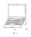
- Fig. 1 is a perspective view of an electronic device according to one embodiment of the invention.
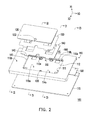
- Fig. 2 is an exploded view of the electronic device in Fig. 1 .
- Fig. 3 is a partial corss-sectional view of the electronic device taken along section line I1-I1 in Fig. 2 .
- the electronic device 100 includes a first case 110, a first protrusion 120, a click pad 130 and a frame 140.
- the electronic device 100 for example, is a notebook computer, but the types of the electronic device 100 of the invention are not limited thereto. Any electronic device which uses the click pad 130 as an input interface could be applied for the present embodiment. It is noted that, only a part of the first case 100 in Fig. 2 is shown for a purpose of clear view.
- the first case 110 has an accommodating cavity 110a, wherein the accommodating cavity 110a is recessed from a surface 110b of the first case 110 and forms a bottom plate 112, a first side wall 114a and a second side wall 114b which are erected on one pair of opposite sides of the bottom plate 112, and two third side walls 115 which are erected on another pair of opposite sides of the bottom plate 112.
- the first protrusion 120 is disposed on the bottom plate 112.
- the click pad 130 has a switch 132.
- the frame 140 is disposed between the first case 110 and the click pad 130, wherein the click pad 130 is assembled in the accommodating cavity 110a by the frame 140, and the switch 132 faces directly to the first protrusion 120.
- the first protrusion 120 is directly disposed on the bottom plate 112 formed by the accommodating cavity 110a and faces directly to the switch 132, the flatness of the first protrusion 120 and the first case 110 after assembled is increased.
- the switch 132 of the click pad 130 is pressed, the pressing stroke of the switch 132 is not affected and not changed by the skewness of the assembly. Therefore, the click pad 130 could provide a good sense of touch.
- the electronic device 100 doesn't need an extra supporting plate for triggering the switch 132 so that the number of elements in the electronic device 100 will be reduced and it is more convenient to assemble the electronic device 100.
- the first case 100 does not need having a big penetration opening so that the structural strength of the electronic device 100 could be well maintained.
- first protrusion 120 and the first case 110 could be formed together by injection molding method, but the invention is not limited thereto.
- a through hole (not shown) is disposed on the bottom plate 112, and the first protrusion 120 penetrates the through hole to be fixed with the first case 110.
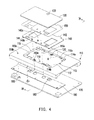
- Fig. 4 is another exploded view of the electronic device in Fig. 1 .
- Fig. 5 is a partially enlarged view of the area A shown in Fig. 4 .
- the first case 110 of the present embodiment further has plural ribs 116 which are disposed in the accommodating cavity 110a and are connected to the bottom plate 112 and the first protrusion 120. Because of this disposition, the connection between the first protrusion 120 and the first case 100 could be strengthened and the sense of touch of the click pad 130 could be maintained.
- the ribs 116 extend and are connected to the first side wall 114a from the bottom plate 112. Therefore, the click pad 130 could further maintain the sense of touch.
- the electronic device 100 further includes an adhesive tape 150 located between the click pad 130 and the frame 140. Therefore, the adhesive tape 150 is used for fixing the click pad 130 firmly to the frame 140.
- the click pad 130 and the frame 140 could be assembled by the lock attached method.
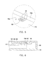
- Fig. 6 is a partial cross-sectional view of the click pad assembled in the accommodating cavity taken along section line I2-I2 in Fig. 2 .
- Fig. 7 is a partial cross-sectional view of the click pad assembled in the accommodating cavity taken along section line I3-I3 in Fig. 2 .
- the frame 140 of the present embodiment has a first hook 142 and a second hook 144, and the first case 110 further has a first opening 110c and a second opening 110d.
- the first hook 142 and the second hook 144 are located at two opposite sides of the frame 140.
- the first opening 110c is disposed on the first side wall 114a, and the second opening 110d is disposed on the bottom plate 112.
- the first hook 142 is inserted into the first opening 110c and the first hook 142 leans against the bottom of the first side wall 114a.
- the frame 140 is pressed in the accommodating cavity 110a so that the second hook 144 is inserted into the second opening 110d and then engages with the bottom of the second side wall 114b.
- the click pad 130 is assembled in the accommodating cavity 110a and limited by the first hook 142 and the second hook 144 so that the click pad 130 could't move along a first direction X1, wherein the first direction X1, for example, is normal to the surface 110b of the first case 110.
- the first case 110 of this embodiment further has a platform 118.
- the platform 118 is disposed on the bottom of the first case 110 and close to the first side wall 114a.
- the first hook 142 contacts the platform 118 when the first hook 142 is inserted into the first opening 110c. Therefore, after the click pad 130 is assembled into the accommodating cavity 110a by the frame 140, the click pad 130 is limited by the platform 118 so that the click pad 130 could not move along a second direction X2, wherein the second direction X2 is paralleled to the two third side walls 115, and the second direction X2 is perpendicular to the first direction X1.
- the frame 140 of the present embodiment has a position limiting slot 140a
- the first case 110 further has a second protrusion 119 disposed on the bottom plate 112.
- the longitudinal direction of the position limiting slot 140a is paralleled with the extension direction of the two third side walls 115, and the position limiting slot 140a is located between the first hook 142 and the second hook 144.
- the second protrusion 119 When the second protrusion 119 is inserted into the position limiting slot 140a, the second protrusion 119 leans against two inner wall surfaces of the position limiting slot 140a, and the click pad 130 is limited so that the click pad 130 could't move along a third direction X3 by the second protrusion 119, wherein the third direction X3 is perpendicular to the first direction X1 or the second direction X2.
- the electronic device 100 further includes a fastener 160.
- the first case 110 further has a first fastening hole 110e disposed on the bottom plate 112, and the frame 140 has a second fastening hole 140b corresponding to the position of the first fastening hole 110e, and the fastener 160 penetrates through the first fastening hole 110e and the second fastening hole 140b so that the frame 140 and the first case 110 are fixed together. Because of this disposition, under the condition that the electronic device 100 is instantly impacted, the frame 140 and the first case 110 are tightly locked and attached to each other so that the click pad 130 could't fall out. Therefore, a high reliability of the electronic 100 could be maintained.
- Fig. 8 is a partial cross-sectional view of the click pad assembled in the accommodating cavity taken along section line I4-I4 in Fig. 4 .
- the electronic device 100 further includes a second case 170 and a bracket 180, wherein the bracket 180 is a component, for example, used for supporting the keyboard 190 (as shown in Fig. 1 ), the second case 170 is assembled in the first case 110 so that the bracket 180 is clamped between the first case 110 and the second case 170.
- the bracket 180 is made by conductive materials, and the bracket 180 and the click pad 130 are electrically connected.
- the circuit board (not shown) of the click pad 130 is connected to the ground through the bracket 180.
- the bracket 180 has a resilient piece 182.
- the resilient piece 182 leans against the click pad 130 to be electrically connected with the bracket 180 and the click pad 130. Because of this disposition, except that the resilient piece 182 is used to connect the circuit board of the click pad 130 to the ground, the resilient piece 182 is also used for supporting the click pad 130 to prevent the situation that the click pad 130 is recessed after long hours of use.
- the frame 140 of the present embodiment has a resilient arm 146 (as shown in FIG. 6 ) that is disposed on the bottom of the frame 140 and the resilient arm 146 leans against the bottom plate 112. Therefore, the click pad 130 is supported on the bottom plate 112 by the resilient arm 146 so that the click pad 130 is less likely to be recessed.
- the resilient piece 182 of the bracket 180 is used to leans against the click pad 130 and be electrically connected with the click pad 130 and the bracket 180, so that the circuit board of the click pad 130 could connect to the ground, wherein the click pad 130 and the bracket 180 are electrically connected to each other by their own method. This part is explained by example as followings.
- Fig. 9 is a partial cross-sectional view of the click pad assembled in the accommodating cavity of another embodiment of the invention.
- the frame 240 has a bonding portion 242 extended from the bottom of the frame 240, and the outside of the bonding portion 242 is coated with a conductive fabric 244.
- the bonding portion 242 leans against the bracket 180 to be electrically connected with the bracket 180 and the click pad 130. Therefore, except that the bonding portion 242 is used to connect the circuit board of the click pad 130 to the ground, the bonding portion 242 could also provide a good support for the click pad 130 to prevent the situation that the click pad 130 is recessed.
- the electronic device of the invention uses the first protrusion, that is directly disposed on the bottom plate of the first case, so that the skewness when assembling of the triggering switch component is reduced and the pressing stroke of the switch is fixed. Therefore, the click pad could provide a good sense of touch.
- the electronic device doesn't need an extra supporting plate for triggering the switch so that the number of elements in the electronic device will be reduced and it is more convenient to assemble the electronic device.
- the first case does not need having a rectangular opening so that the structural strength of the electronic device could be well maintained.
- the click pad could be connected to the ground.
- the bracket has the resilient piece or the frame has the resilient arm, the click pad could be supported to prevent the recession of the click pad.
Landscapes
- Engineering & Computer Science (AREA)
- Theoretical Computer Science (AREA)
- General Engineering & Computer Science (AREA)
- Human Computer Interaction (AREA)
- Physics & Mathematics (AREA)
- General Physics & Mathematics (AREA)
- Computer Hardware Design (AREA)
- Casings For Electric Apparatus (AREA)
- Position Input By Displaying (AREA)
- Push-Button Switches (AREA)
Abstract
Description
- The invention relates to an electronic device and more particularly to an electronic device having a click pad.
- As the technology industries develop in recent years, electronic devices, such as notebook computer, tablet PC, or smart phone, are frequently used in our daily life. Types and functions of the electronic devices are increasingly diversified, and the electronic devices are more popular due to convenience and practicality thereof and can be used for different purposes.
- The electronic device, such as a notebook computer, is generally configured to have a keyboard and a click pad as input interfaces. The click pad usually corresponds to a switch, which is disposed inside the electronic device, so that the user can trigger the switch by single-clicking or double-clicking on the click pad.
- Generally, a rectangular opening is disposed on a case of a traditional notebook computer, and the click pad is installed in the rectangular opening. Furthermore, a supporting plate is disposed below the click pad and used to trigger the above-mentioned switch. However, when the supporting plate is assembled, the flatness of the supporting plate needs being well maintained to help the user can retain a good sense of touch, so that the assembling condition is stricter. In addition, if the case has a penetration opening, the structural strength of the case will decrease.
- It is an object of the present invention to provide an enhanced electronic device having a click pad that provides for the user a good sense of touch, that does not require a large penetration opening so that the structural strength of the entire electronic device can be well maintained and that can be manufactured and assembled in a simple and cost-efficient manner.
- This problem is solved by an electronic device having a click pad as claimed in claim 1. Further advantageous embodiments are the subject-matter of the dependent claims.
- The electronic device according to the present invention comprises a first case (casing), a first protrusion, the click pad and a frame. The first case has an accommodating cavity, wherein the accommodating cavity is recessed from a surface of the first case and forms a bottom plate, a first side wall and a second side wall which are erected on one pair of opposite sides of the bottom plate, and two third side walls which are erected on another pair of opposite sides of the bottom plate. The first protrusion is disposed on the bottom plate. The click pad has a switch. The frame is disposed between the first case and the click pad, wherein the click pad is assembled in the accommodating cavity by the frame, and the switch faces directly to the first protrusion.
- In summary, in the electronic device according to the present invention, when the click pad is assembled into the accommodating cavity of the first case by the frame, the first protrusion disposed on the bottom plate of the case faces directly to the switch of the click pad. The switch of the click pad is triggered by the first protrusion that is disposed on the bottom plate formed by the accommodating cavity, so that the flatness between the first protrusion and the first case is increased (enhanced), and the pressing stroke of the switch is not affected and not changed by the flatness. Therefore, the click pad can provide a good sense of touch for a user. In addition, the case does not need to have a big penetration opening so that the structural strength of the electronic device according to the present application can be well maintained.
- To make the aforesaid features and advantages of the invention more comprehensible, several embodiments accompanied with drawings are described in details as follows.
-
- Fig. 1
- is a perspective view of an electronic device according to one embodiment of the invention.
- Fig. 2
- is an exploded view of the electronic device in
Fig. 1 . - Fig. 3
- is a partial cross-sectional view of a click pad assembled in an accommodating cavity taken along section line I1-I1 in
Fig. 2 . - Fig. 4
- is another exploded view of the electronic device in
Fig. 1 . - Fig. 5
- is a partially enlarged view of the area A shown in
Fig. 4 . - Fig. 6
- is a partial cross-sectional view of the click pad assembled in the accommodating cavity taken along section line I2-I2 in
Fig. 2 . - Fig. 7
- is a partial cross-sectional view of the click pad assembled in the accommodating cavity taken along section line I3-I3 in
Fig. 2 . - Fig. 8
- is a partial cross-sectional view of the click pad assembled in the accommodating cavity taken along section line I4-I4 in
Fig. 4 . - Fig. 9
- is a partial cross-sectional view of the click pad assembled in the accommodating cavity of another embodiment of the invention.
-
Fig. 1 is a perspective view of an electronic device according to one embodiment of the invention.Fig. 2 is an exploded view of the electronic device inFig. 1 .Fig. 3 is a partial corss-sectional view of the electronic device taken along section line I1-I1 inFig. 2 . Referring toFig. 1 ,Fig. 2 andFig. 3 , in the present embodiment, theelectronic device 100 includes afirst case 110, afirst protrusion 120, aclick pad 130 and aframe 140. In addition, theelectronic device 100, for example, is a notebook computer, but the types of theelectronic device 100 of the invention are not limited thereto. Any electronic device which uses theclick pad 130 as an input interface could be applied for the present embodiment. It is noted that, only a part of thefirst case 100 inFig. 2 is shown for a purpose of clear view. - The
first case 110 has anaccommodating cavity 110a, wherein theaccommodating cavity 110a is recessed from asurface 110b of thefirst case 110 and forms abottom plate 112, afirst side wall 114a and asecond side wall 114b which are erected on one pair of opposite sides of thebottom plate 112, and twothird side walls 115 which are erected on another pair of opposite sides of thebottom plate 112. Thefirst protrusion 120 is disposed on thebottom plate 112. Theclick pad 130 has aswitch 132. Theframe 140 is disposed between thefirst case 110 and theclick pad 130, wherein theclick pad 130 is assembled in theaccommodating cavity 110a by theframe 140, and theswitch 132 faces directly to thefirst protrusion 120. Because thefirst protrusion 120 is directly disposed on thebottom plate 112 formed by theaccommodating cavity 110a and faces directly to theswitch 132, the flatness of thefirst protrusion 120 and thefirst case 110 after assembled is increased. When theswitch 132 of theclick pad 130 is pressed, the pressing stroke of theswitch 132 is not affected and not changed by the skewness of the assembly. Therefore, theclick pad 130 could provide a good sense of touch. In addition, theelectronic device 100 doesn't need an extra supporting plate for triggering theswitch 132 so that the number of elements in theelectronic device 100 will be reduced and it is more convenient to assemble theelectronic device 100. Furthermore, thefirst case 100 does not need having a big penetration opening so that the structural strength of theelectronic device 100 could be well maintained. - In this embodiment, the
first protrusion 120 and thefirst case 110 could be formed together by injection molding method, but the invention is not limited thereto. In other embodiments, a through hole (not shown) is disposed on thebottom plate 112, and thefirst protrusion 120 penetrates the through hole to be fixed with thefirst case 110. -
Fig. 4 is another exploded view of the electronic device inFig. 1 .Fig. 5 is a partially enlarged view of the area A shown inFig. 4 . Referring toFig. 2 ,Fig. 4 andFig. 5 , thefirst case 110 of the present embodiment further hasplural ribs 116 which are disposed in theaccommodating cavity 110a and are connected to thebottom plate 112 and thefirst protrusion 120. Because of this disposition, the connection between thefirst protrusion 120 and thefirst case 100 could be strengthened and the sense of touch of theclick pad 130 could be maintained. In addition, theribs 116 extend and are connected to thefirst side wall 114a from thebottom plate 112. Therefore, theclick pad 130 could further maintain the sense of touch. - Referring to
Fig. 2 andFig. 4 , in the present embodiment, theelectronic device 100 further includes anadhesive tape 150 located between theclick pad 130 and theframe 140. Therefore, theadhesive tape 150 is used for fixing theclick pad 130 firmly to theframe 140. In addition, in other embodiments, theclick pad 130 and theframe 140 could be assembled by the lock attached method. -
Fig. 6 is a partial cross-sectional view of the click pad assembled in the accommodating cavity taken along section line I2-I2 inFig. 2 .Fig. 7 is a partial cross-sectional view of the click pad assembled in the accommodating cavity taken along section line I3-I3 inFig. 2 . Referring toFig. 2 ,Fig. 4 ,Fig. 6 andFig. 7 , theframe 140 of the present embodiment has afirst hook 142 and asecond hook 144, and thefirst case 110 further has afirst opening 110c and asecond opening 110d. Thefirst hook 142 and thesecond hook 144 are located at two opposite sides of theframe 140. Thefirst opening 110c is disposed on thefirst side wall 114a, and thesecond opening 110d is disposed on thebottom plate 112. Thefirst hook 142 is inserted into thefirst opening 110c and thefirst hook 142 leans against the bottom of thefirst side wall 114a. After that, theframe 140 is pressed in theaccommodating cavity 110a so that thesecond hook 144 is inserted into thesecond opening 110d and then engages with the bottom of thesecond side wall 114b. Hence, theclick pad 130 is assembled in theaccommodating cavity 110a and limited by thefirst hook 142 and thesecond hook 144 so that theclick pad 130 couldn't move along a first direction X1, wherein the first direction X1, for example, is normal to thesurface 110b of thefirst case 110. - In addition, the
first case 110 of this embodiment further has aplatform 118. Theplatform 118 is disposed on the bottom of thefirst case 110 and close to thefirst side wall 114a. Thefirst hook 142 contacts theplatform 118 when thefirst hook 142 is inserted into thefirst opening 110c. Therefore, after theclick pad 130 is assembled into theaccommodating cavity 110a by theframe 140, theclick pad 130 is limited by theplatform 118 so that theclick pad 130 could not move along a second direction X2, wherein the second direction X2 is paralleled to the twothird side walls 115, and the second direction X2 is perpendicular to the first direction X1. - Furthermore, the
frame 140 of the present embodiment has aposition limiting slot 140a, and thefirst case 110 further has asecond protrusion 119 disposed on thebottom plate 112. The longitudinal direction of theposition limiting slot 140a is paralleled with the extension direction of the twothird side walls 115, and theposition limiting slot 140a is located between thefirst hook 142 and thesecond hook 144. When thesecond protrusion 119 is inserted into theposition limiting slot 140a, thesecond protrusion 119 leans against two inner wall surfaces of theposition limiting slot 140a, and theclick pad 130 is limited so that theclick pad 130 couldn't move along a third direction X3 by thesecond protrusion 119, wherein the third direction X3 is perpendicular to the first direction X1 or the second direction X2. - In this embodiment, the
electronic device 100 further includes afastener 160. Thefirst case 110 further has afirst fastening hole 110e disposed on thebottom plate 112, and theframe 140 has asecond fastening hole 140b corresponding to the position of thefirst fastening hole 110e, and thefastener 160 penetrates through thefirst fastening hole 110e and thesecond fastening hole 140b so that theframe 140 and thefirst case 110 are fixed together. Because of this disposition, under the condition that theelectronic device 100 is instantly impacted, theframe 140 and thefirst case 110 are tightly locked and attached to each other so that theclick pad 130 couldn't fall out. Therefore, a high reliability of the electronic 100 could be maintained. -
Fig. 8 is a partial cross-sectional view of the click pad assembled in the accommodating cavity taken along section line I4-I4 inFig. 4 . Referring toFig. 2 ,Fig. 4 andFig. 8 , in the present embodiment, theelectronic device 100 further includes asecond case 170 and abracket 180, wherein thebracket 180 is a component, for example, used for supporting the keyboard 190 (as shown inFig. 1 ), thesecond case 170 is assembled in thefirst case 110 so that thebracket 180 is clamped between thefirst case 110 and thesecond case 170. Thebracket 180 is made by conductive materials, and thebracket 180 and theclick pad 130 are electrically connected. Because of this disposition, the circuit board (not shown) of theclick pad 130 is connected to the ground through thebracket 180. In addition, thebracket 180 has aresilient piece 182. Theresilient piece 182 leans against theclick pad 130 to be electrically connected with thebracket 180 and theclick pad 130. Because of this disposition, except that theresilient piece 182 is used to connect the circuit board of theclick pad 130 to the ground, theresilient piece 182 is also used for supporting theclick pad 130 to prevent the situation that theclick pad 130 is recessed after long hours of use. - Base on the above, the
frame 140 of the present embodiment has a resilient arm 146 (as shown inFIG. 6 ) that is disposed on the bottom of theframe 140 and theresilient arm 146 leans against thebottom plate 112. Therefore, theclick pad 130 is supported on thebottom plate 112 by theresilient arm 146 so that theclick pad 130 is less likely to be recessed. - In addition, in the
electronic device 100 of the present embodiment, theresilient piece 182 of thebracket 180 is used to leans against theclick pad 130 and be electrically connected with theclick pad 130 and thebracket 180, so that the circuit board of theclick pad 130 could connect to the ground, wherein theclick pad 130 and thebracket 180 are electrically connected to each other by their own method. This part is explained by example as followings. -
Fig. 9 is a partial cross-sectional view of the click pad assembled in the accommodating cavity of another embodiment of the invention. Referring toFIG. 9 , in the present embodiment, theframe 240 has abonding portion 242 extended from the bottom of theframe 240, and the outside of thebonding portion 242 is coated with aconductive fabric 244. Thebonding portion 242 leans against thebracket 180 to be electrically connected with thebracket 180 and theclick pad 130. Therefore, except that thebonding portion 242 is used to connect the circuit board of theclick pad 130 to the ground, thebonding portion 242 could also provide a good support for theclick pad 130 to prevent the situation that theclick pad 130 is recessed. - In summary, the electronic device of the invention uses the first protrusion, that is directly disposed on the bottom plate of the first case, so that the skewness when assembling of the triggering switch component is reduced and the pressing stroke of the switch is fixed. Therefore, the click pad could provide a good sense of touch. In addition, the electronic device doesn't need an extra supporting plate for triggering the switch so that the number of elements in the electronic device will be reduced and it is more convenient to assemble the electronic device. Furthermore, the first case does not need having a rectangular opening so that the structural strength of the electronic device could be well maintained. In addition, when this invention has the bracket, the click pad could be connected to the ground. Furthermore, when the bracket has the resilient piece or the frame has the resilient arm, the click pad could be supported to prevent the recession of the click pad.
Claims (12)
- An electronic device (100), comprising:a first case (110), having an accommodating cavity (110a), wherein the accommodating cavity (110a) is recessed from a surface (110b) of the first case (110) and the accommodating cavity (110a) forms a bottom plate (112), a first side wall (114a) and a second side wall (114b) erected on one pair of opposite sides of the bottom plate (112), and two third side walls (115) erected on another pair of opposite sides of the bottom plate (112);a first protrusion (120), disposed on the bottom plate (112);a click pad (130), having a switch (132); anda frame (140), disposed between the first case (110) and the click pad (130), whereinthe click pad (130) is assembled in the accommodating cavity (110a) by the frame (140), andthe switch (132) faces directly to the first protrusion (120).
- The electronic device (100) as claimed in claim 1, further comprising a second case (170) and a bracket (180), wherein
the second case (170) is assembled to the first case (110) so that the bracket (180) is clamped between the first case (110) and the second case (170),
the bracket (180) is made by conductive materials, and
the bracket (180) and the click pad (130) are electrically connected. - The electronic device (100) as claimed in claim 2, wherein
the bracket has a resilient piece (182),
the resilient piece (182) leans against the click pad (130) and
the resilient piece (182) is electrically connected with the bracket (180) and the click pad (130). - The electronic device (100) as claimed in claim 2 or 3, wherein the frame (240) has a bonding portion (242) extended from the bottom of the frame (240), and the bonding portion (242) is electrically conductive and leans against the bracket (180) to be electrically connected with the bracket (180) and the click pad (130).
- The electronic device (100) as claimed in any of the preceding claims, wherein the frame has a resilient arm (146) disposed on the bottom of the frame (140) and the resilient arm (140) leans against the bottom plate (112).
- The electronic device (100) as claimed in any of the preceding claims, wherein the frame has a first hook (142) and a second hook (144), and the first case (110) further has a first opening (110c) and a second opening (110d), the first hook (142) and the second hook (144) are located at two sides of the frame (140), the first opening (110c) is disposed on the first side wall (114a), and the second opening (110d) is disposed on the bottom plate (112), the first hook (142) is inserted into the first opening (110c) and leans against the bottom of the first side wall (114a), the second hook (144) is inserted into the second opening (110d) and the second hook (144) engages with the bottom of the second side wall (114b).
- The electronic device (100) as claimed in claim 6, wherein the first case further has a platform (118) disposed on the bottom of the first case (110), when the first hook (142) is inserted into the first opening (110c), the first hook (142) contacts the platform (118), and the click pad (130) is limited by the platform (118).
- The electronic device (100) as claimed in claim 6 or 7, wherein the frame (140) has a position limiting slot (140a), and the first case (110) further has a second protrusion (119) disposed on the bottom plate (112), the position limiting slot (140a) is paralleled with the two third side walls (115) and located between the first hook (142) and the second hook (144), when the second protrusion (119) is inserted into the position limiting slot (140a), the click pad (130) is limited by the second protrusion (119).
- The electronic device (100) as claimed in any of the preceding claims, further comprising a fastener (160), wherein the first case (110) further has a first fastening hole (110e) disposed on the bottom plate (112), and the frame (140) has a second fastening hole (140b) corresponding to a position of the first fastening hole (110e), and the fastener (160) is penetrated through the first fastening hole (110e) and the second fastening hole (140b).
- The electronic device (100) as claimed in any of the preceding claims, wherein the first case has at least one rib (116) disposed in the accommodating cavity (110a) and the rib (116) is connected to the bottom plate (112) and the first protrusion (120).
- The electronic device (100) as claimed in claim 10, wherein the rib (116) extends and is connected to the first side wall (114a) from the bottom plate (112).
- The electronic device (100) as claimed in any of the preceding claims, further comprising an adhesive tape (150) located between the click pad (130) and the frame (140).
Applications Claiming Priority (1)
| Application Number | Priority Date | Filing Date | Title |
|---|---|---|---|
| TW104107631A TWI557535B (en) | 2015-03-10 | 2015-03-10 | Electronic device |
Publications (2)
| Publication Number | Publication Date |
|---|---|
| EP3067785A1 true EP3067785A1 (en) | 2016-09-14 |
| EP3067785B1 EP3067785B1 (en) | 2018-09-19 |
Family
ID=53716361
Family Applications (1)
| Application Number | Title | Priority Date | Filing Date |
|---|---|---|---|
| EP15177064.1A Not-in-force EP3067785B1 (en) | 2015-03-10 | 2015-07-16 | Electronic device |
Country Status (4)
| Country | Link |
|---|---|
| US (1) | US9465416B2 (en) |
| EP (1) | EP3067785B1 (en) |
| CN (1) | CN106155189B (en) |
| TW (1) | TWI557535B (en) |
Families Citing this family (23)
| Publication number | Priority date | Publication date | Assignee | Title |
|---|---|---|---|---|
| CN106527819A (en) * | 2016-12-20 | 2017-03-22 | 合肥联宝信息技术有限公司 | Touch mechanism and electronic equipment |
| TWI658388B (en) * | 2018-04-12 | 2019-05-01 | 群光電子股份有限公司 | Touch pad device |
| TWI664890B (en) * | 2018-04-13 | 2019-07-01 | 精元電腦股份有限公司 | Touch device |
| TWI663504B (en) * | 2018-06-15 | 2019-06-21 | 致伸科技股份有限公司 | Touch pad module |
| TWI672622B (en) * | 2018-08-09 | 2019-09-21 | 群光電子股份有限公司 | Electronic device and click pad thereof |
| CN110837273B (en) * | 2018-08-16 | 2023-12-08 | 群光电子(苏州)有限公司 | Electronic device and touch pad thereof |
| TWI676923B (en) * | 2018-10-25 | 2019-11-11 | 群光電子股份有限公司 | Touchpad device |
| TWI714036B (en) * | 2019-03-22 | 2020-12-21 | 致伸科技股份有限公司 | Touch pad module |
| CN112486358B (en) * | 2020-03-06 | 2024-05-28 | 光宝电子(广州)有限公司 | Touch control device |
| TWI725772B (en) * | 2020-03-13 | 2021-04-21 | 致伸科技股份有限公司 | Touch pad module and computer device using the same |
| TWI738368B (en) | 2020-06-01 | 2021-09-01 | 群光電子股份有限公司 | Touchpad device |
| TWI755095B (en) * | 2020-10-13 | 2022-02-11 | 群光電子股份有限公司 | Touchpad device |
| TWD214178S (en) * | 2020-12-10 | 2021-09-21 | 宏碁股份有限公司 | Notebook computer |
| TWM617205U (en) * | 2021-03-02 | 2021-09-21 | 宏碁股份有限公司 | Touchpad mechanism |
| TWI773237B (en) * | 2021-04-08 | 2022-08-01 | 群光電子股份有限公司 | Touchpad device |
| CN115202439B (en) * | 2021-04-12 | 2025-07-29 | 群光电子(苏州)有限公司 | Touch control panel device |
| TWI775432B (en) * | 2021-05-12 | 2022-08-21 | 群光電子股份有限公司 | Touchpad device |
| CN115344082B (en) * | 2021-05-14 | 2025-07-29 | 群光电子(苏州)有限公司 | Touch control panel device |
| WO2023225770A1 (en) | 2022-05-23 | 2023-11-30 | 深圳市汇顶科技股份有限公司 | Supporting assembly, touchpad and electronic device |
| CN114637373A (en) | 2022-03-11 | 2022-06-17 | 深圳市汇顶科技股份有限公司 | Touch panel module and electronic device using the touch panel module |
| CN114637413B (en) * | 2022-03-24 | 2025-02-25 | 东莞华贝电子科技有限公司 | Touch panel installation structure, touch module and electronic equipment |
| TWI817841B (en) * | 2022-11-23 | 2023-10-01 | 宏碁股份有限公司 | Body structure of portable computer |
| US12242676B2 (en) * | 2023-06-23 | 2025-03-04 | Apple Inc. | Input device |
Citations (2)
| Publication number | Priority date | Publication date | Assignee | Title |
|---|---|---|---|---|
| US20110080354A1 (en) * | 2009-10-05 | 2011-04-07 | Quanta Computer Inc. | Touch pad module assembly structure |
| WO2013142468A1 (en) * | 2012-03-20 | 2013-09-26 | Google Inc. | Fully clickable trackpad |
Family Cites Families (38)
| Publication number | Priority date | Publication date | Assignee | Title |
|---|---|---|---|---|
| US5287246A (en) * | 1992-05-27 | 1994-02-15 | Orete Systems, Inc. | Drawer type track ball for portable computers |
| US5339213A (en) * | 1992-11-16 | 1994-08-16 | Cirque Corporation | Portable computer touch pad attachment |
| US5546334A (en) * | 1993-03-29 | 1996-08-13 | Acer Incorporated | Notebook computer system with a separable trackball |
| JP2914923B2 (en) * | 1996-10-29 | 1999-07-05 | 三菱電機株式会社 | Small electronic equipment having a pointing device |
| US5793355A (en) * | 1997-03-03 | 1998-08-11 | Compaq Computer Corporation | Portable computer with interchangeable pointing device modules |
| US6163326A (en) * | 1998-02-26 | 2000-12-19 | Micron Electronics, Inc. | Input device for a laptop computer |
| US6281887B1 (en) * | 1999-09-20 | 2001-08-28 | Mitac International Corp. | Touchpad assembly |
| US6476795B1 (en) * | 2000-01-20 | 2002-11-05 | Hewlett-Packard Company | Mouse recharging module |
| TWM242790U (en) * | 2002-11-22 | 2004-09-01 | Compal Electronics Inc | Electronic equipment having retrievable touch panel |
| US7633492B2 (en) * | 2003-01-15 | 2009-12-15 | Asustek Computer Inc. | Notebook computer with hidden touch pad |
| TWI232398B (en) * | 2004-02-12 | 2005-05-11 | Asustek Comp Inc | Electronic apparatus and button structure |
| US20070205919A1 (en) * | 2006-03-01 | 2007-09-06 | Inventec Corporation | Changeable panel structure |
| JP2007287122A (en) * | 2006-03-20 | 2007-11-01 | Fujitsu Ltd | Electronic equipment and programs |
| TWM298181U (en) * | 2006-04-25 | 2006-09-21 | Inventec Corp | Elastic pressing and fixing component |
| US8803806B2 (en) * | 2007-01-23 | 2014-08-12 | Dell Products L.P. | Notebook computer having an off-motherboard keyboard controller |
| KR101391759B1 (en) * | 2007-04-25 | 2014-05-07 | 삼성전자 주식회사 | Portable computer |
| KR101380749B1 (en) * | 2007-04-25 | 2014-04-03 | 삼성전자 주식회사 | Portable computer |
| DE602007009829D1 (en) * | 2007-08-13 | 2010-11-25 | Research In Motion Ltd | Tactile touchscreen for an electronic device |
| US8294675B2 (en) * | 2008-01-04 | 2012-10-23 | Apple Inc. | Touchpad and pick button assembly |
| JP2009301144A (en) * | 2008-06-10 | 2009-12-24 | Fujitsu Ltd | Electronic device |
| US8441450B2 (en) * | 2008-09-30 | 2013-05-14 | Apple Inc. | Movable track pad with added functionality |
| CN101937257A (en) * | 2009-06-29 | 2011-01-05 | 鸿富锦精密工业(深圳)有限公司 | laptop |
| JP4751470B2 (en) * | 2009-12-18 | 2011-08-17 | 株式会社東芝 | Electronics |
| CN102221916A (en) * | 2010-04-15 | 2011-10-19 | 昌硕科技(上海)有限公司 | Movable touch module and electronic device applying same |
| CN102243930A (en) * | 2010-05-13 | 2011-11-16 | 英业达股份有限公司 | Structure for improving touch feeling of key |
| JP5696475B2 (en) * | 2010-12-28 | 2015-04-08 | 富士通株式会社 | Fixing parts and electronic equipment |
| CN102810022A (en) * | 2011-06-03 | 2012-12-05 | 鸿富锦精密工业(深圳)有限公司 | Touch device and electronic equipment with touch device |
| CN102819288A (en) * | 2011-06-09 | 2012-12-12 | 鸿富锦精密工业(深圳)有限公司 | Notebook computer |
| TWI464561B (en) * | 2012-01-04 | 2014-12-11 | Wistron Corp | Thin touch pad module and related manufacturing method |
| JP5889661B2 (en) * | 2012-02-10 | 2016-03-22 | アルプス電気株式会社 | Input device |
| CN202502927U (en) * | 2012-03-08 | 2012-10-24 | 纬创资通股份有限公司 | Key module and electronic device with key module |
| TWI486818B (en) * | 2012-05-25 | 2015-06-01 | 緯創資通股份有限公司 | Input device and electronic device |
| TWI519925B (en) * | 2012-10-12 | 2016-02-01 | 緯創資通股份有限公司 | A controlling device for turning on/off pressed-key function of a click pad |
| CN103729021B (en) * | 2012-10-15 | 2018-09-11 | 鸿富锦精密工业(深圳)有限公司 | Cursor moves module |
| US9030839B2 (en) * | 2012-10-18 | 2015-05-12 | Apple Inc. | Track pad acoustic features related to a portable computer |
| JP2014085941A (en) * | 2012-10-25 | 2014-05-12 | Toshiba Corp | Electronic apparatus |
| TWM459666U (en) * | 2013-01-22 | 2013-08-11 | Acer Inc | Touch pad module and electronic device |
| JP6080265B2 (en) * | 2013-12-26 | 2017-02-15 | アルプス電気株式会社 | Touchpad input device |
-
2015
- 2015-03-10 TW TW104107631A patent/TWI557535B/en not_active IP Right Cessation
- 2015-04-13 CN CN201510170753.1A patent/CN106155189B/en not_active Expired - Fee Related
- 2015-07-01 US US14/788,816 patent/US9465416B2/en active Active
- 2015-07-16 EP EP15177064.1A patent/EP3067785B1/en not_active Not-in-force
Patent Citations (2)
| Publication number | Priority date | Publication date | Assignee | Title |
|---|---|---|---|---|
| US20110080354A1 (en) * | 2009-10-05 | 2011-04-07 | Quanta Computer Inc. | Touch pad module assembly structure |
| WO2013142468A1 (en) * | 2012-03-20 | 2013-09-26 | Google Inc. | Fully clickable trackpad |
Also Published As
| Publication number | Publication date |
|---|---|
| CN106155189A (en) | 2016-11-23 |
| TW201633042A (en) | 2016-09-16 |
| EP3067785B1 (en) | 2018-09-19 |
| US20160266617A1 (en) | 2016-09-15 |
| CN106155189B (en) | 2019-06-25 |
| US9465416B2 (en) | 2016-10-11 |
| TWI557535B (en) | 2016-11-11 |
Similar Documents
| Publication | Publication Date | Title |
|---|---|---|
| EP3067785B1 (en) | Electronic device | |
| CN105072220B (en) | Electronic equipment and key-press mounting structure | |
| US7800008B2 (en) | Side key assembly and electronic device using the same | |
| US10180739B2 (en) | Input device for a portable electronic apparatus | |
| CN107317136B (en) | A kind of USB interface component and mobile terminal | |
| US20120018291A1 (en) | Switch assembly | |
| US20080050941A1 (en) | Electrical connector with retaining shell | |
| US20090040713A1 (en) | Server enclosure | |
| CN110299606A (en) | Electronic equipment and its elastic slice component, elastic slice | |
| TWI822752B (en) | Electronic device and side key structure | |
| US8281480B2 (en) | Method for manufacturing wireless receiver | |
| WO2017173730A1 (en) | Side button and terminal | |
| US20070133187A1 (en) | Electronic device having a grounded structure | |
| JP2015211069A (en) | Electronics | |
| US9086857B2 (en) | Fastening device for expansion card | |
| US8243457B2 (en) | Electronic component mounting structure, electronic device and manufacturing method of an electronic device | |
| CN114121533A (en) | Key assembly, shell and electronic equipment | |
| JP6674121B1 (en) | Electronics | |
| CN103917063A (en) | Electronic equipment | |
| JP2019040560A (en) | Keyboard cover | |
| US8212166B2 (en) | Switch assembly | |
| US20140111936A1 (en) | Electronic device with airflow guide cover having intrusion switch | |
| CN115223811A (en) | A key structure and electronic product | |
| US20050225528A1 (en) | Electronic device | |
| CN218974897U (en) | Touch panel device |
Legal Events
| Date | Code | Title | Description |
|---|---|---|---|
| PUAI | Public reference made under article 153(3) epc to a published international application that has entered the european phase |
Free format text: ORIGINAL CODE: 0009012 |
|
| 17P | Request for examination filed |
Effective date: 20160707 |
|
| AK | Designated contracting states |
Kind code of ref document: A1 Designated state(s): AL AT BE BG CH CY CZ DE DK EE ES FI FR GB GR HR HU IE IS IT LI LT LU LV MC MK MT NL NO PL PT RO RS SE SI SK SM TR |
|
| AX | Request for extension of the european patent |
Extension state: BA ME |
|
| STAA | Information on the status of an ep patent application or granted ep patent |
Free format text: STATUS: EXAMINATION IS IN PROGRESS |
|
| 17Q | First examination report despatched |
Effective date: 20170614 |
|
| GRAP | Despatch of communication of intention to grant a patent |
Free format text: ORIGINAL CODE: EPIDOSNIGR1 |
|
| STAA | Information on the status of an ep patent application or granted ep patent |
Free format text: STATUS: GRANT OF PATENT IS INTENDED |
|
| INTG | Intention to grant announced |
Effective date: 20180515 |
|
| GRAS | Grant fee paid |
Free format text: ORIGINAL CODE: EPIDOSNIGR3 |
|
| GRAA | (expected) grant |
Free format text: ORIGINAL CODE: 0009210 |
|
| STAA | Information on the status of an ep patent application or granted ep patent |
Free format text: STATUS: THE PATENT HAS BEEN GRANTED |
|
| AK | Designated contracting states |
Kind code of ref document: B1 Designated state(s): AL AT BE BG CH CY CZ DE DK EE ES FI FR GB GR HR HU IE IS IT LI LT LU LV MC MK MT NL NO PL PT RO RS SE SI SK SM TR |
|
| REG | Reference to a national code |
Ref country code: GB Ref legal event code: FG4D |
|
| REG | Reference to a national code |
Ref country code: CH Ref legal event code: EP |
|
| REG | Reference to a national code |
Ref country code: AT Ref legal event code: REF Ref document number: 1044002 Country of ref document: AT Kind code of ref document: T Effective date: 20181015 |
|
| REG | Reference to a national code |
Ref country code: IE Ref legal event code: FG4D |
|
| REG | Reference to a national code |
Ref country code: DE Ref legal event code: R096 Ref document number: 602015016496 Country of ref document: DE |
|
| REG | Reference to a national code |
Ref country code: NL Ref legal event code: MP Effective date: 20180919 |
|
| PG25 | Lapsed in a contracting state [announced via postgrant information from national office to epo] |
Ref country code: FI Free format text: LAPSE BECAUSE OF FAILURE TO SUBMIT A TRANSLATION OF THE DESCRIPTION OR TO PAY THE FEE WITHIN THE PRESCRIBED TIME-LIMIT Effective date: 20180919 Ref country code: RS Free format text: LAPSE BECAUSE OF FAILURE TO SUBMIT A TRANSLATION OF THE DESCRIPTION OR TO PAY THE FEE WITHIN THE PRESCRIBED TIME-LIMIT Effective date: 20180919 Ref country code: NO Free format text: LAPSE BECAUSE OF FAILURE TO SUBMIT A TRANSLATION OF THE DESCRIPTION OR TO PAY THE FEE WITHIN THE PRESCRIBED TIME-LIMIT Effective date: 20181219 Ref country code: SE Free format text: LAPSE BECAUSE OF FAILURE TO SUBMIT A TRANSLATION OF THE DESCRIPTION OR TO PAY THE FEE WITHIN THE PRESCRIBED TIME-LIMIT Effective date: 20180919 Ref country code: BG Free format text: LAPSE BECAUSE OF FAILURE TO SUBMIT A TRANSLATION OF THE DESCRIPTION OR TO PAY THE FEE WITHIN THE PRESCRIBED TIME-LIMIT Effective date: 20181219 Ref country code: LT Free format text: LAPSE BECAUSE OF FAILURE TO SUBMIT A TRANSLATION OF THE DESCRIPTION OR TO PAY THE FEE WITHIN THE PRESCRIBED TIME-LIMIT Effective date: 20180919 Ref country code: GR Free format text: LAPSE BECAUSE OF FAILURE TO SUBMIT A TRANSLATION OF THE DESCRIPTION OR TO PAY THE FEE WITHIN THE PRESCRIBED TIME-LIMIT Effective date: 20181220 |
|
| REG | Reference to a national code |
Ref country code: LT Ref legal event code: MG4D |
|
| PG25 | Lapsed in a contracting state [announced via postgrant information from national office to epo] |
Ref country code: HR Free format text: LAPSE BECAUSE OF FAILURE TO SUBMIT A TRANSLATION OF THE DESCRIPTION OR TO PAY THE FEE WITHIN THE PRESCRIBED TIME-LIMIT Effective date: 20180919 Ref country code: LV Free format text: LAPSE BECAUSE OF FAILURE TO SUBMIT A TRANSLATION OF THE DESCRIPTION OR TO PAY THE FEE WITHIN THE PRESCRIBED TIME-LIMIT Effective date: 20180919 Ref country code: AL Free format text: LAPSE BECAUSE OF FAILURE TO SUBMIT A TRANSLATION OF THE DESCRIPTION OR TO PAY THE FEE WITHIN THE PRESCRIBED TIME-LIMIT Effective date: 20180919 |
|
| REG | Reference to a national code |
Ref country code: AT Ref legal event code: MK05 Ref document number: 1044002 Country of ref document: AT Kind code of ref document: T Effective date: 20180919 |
|
| PG25 | Lapsed in a contracting state [announced via postgrant information from national office to epo] |
Ref country code: RO Free format text: LAPSE BECAUSE OF FAILURE TO SUBMIT A TRANSLATION OF THE DESCRIPTION OR TO PAY THE FEE WITHIN THE PRESCRIBED TIME-LIMIT Effective date: 20180919 Ref country code: NL Free format text: LAPSE BECAUSE OF FAILURE TO SUBMIT A TRANSLATION OF THE DESCRIPTION OR TO PAY THE FEE WITHIN THE PRESCRIBED TIME-LIMIT Effective date: 20180919 Ref country code: CZ Free format text: LAPSE BECAUSE OF FAILURE TO SUBMIT A TRANSLATION OF THE DESCRIPTION OR TO PAY THE FEE WITHIN THE PRESCRIBED TIME-LIMIT Effective date: 20180919 Ref country code: IS Free format text: LAPSE BECAUSE OF FAILURE TO SUBMIT A TRANSLATION OF THE DESCRIPTION OR TO PAY THE FEE WITHIN THE PRESCRIBED TIME-LIMIT Effective date: 20190119 Ref country code: ES Free format text: LAPSE BECAUSE OF FAILURE TO SUBMIT A TRANSLATION OF THE DESCRIPTION OR TO PAY THE FEE WITHIN THE PRESCRIBED TIME-LIMIT Effective date: 20180919 Ref country code: PL Free format text: LAPSE BECAUSE OF FAILURE TO SUBMIT A TRANSLATION OF THE DESCRIPTION OR TO PAY THE FEE WITHIN THE PRESCRIBED TIME-LIMIT Effective date: 20180919 Ref country code: EE Free format text: LAPSE BECAUSE OF FAILURE TO SUBMIT A TRANSLATION OF THE DESCRIPTION OR TO PAY THE FEE WITHIN THE PRESCRIBED TIME-LIMIT Effective date: 20180919 Ref country code: IT Free format text: LAPSE BECAUSE OF FAILURE TO SUBMIT A TRANSLATION OF THE DESCRIPTION OR TO PAY THE FEE WITHIN THE PRESCRIBED TIME-LIMIT Effective date: 20180919 Ref country code: AT Free format text: LAPSE BECAUSE OF FAILURE TO SUBMIT A TRANSLATION OF THE DESCRIPTION OR TO PAY THE FEE WITHIN THE PRESCRIBED TIME-LIMIT Effective date: 20180919 |
|
| PG25 | Lapsed in a contracting state [announced via postgrant information from national office to epo] |
Ref country code: SM Free format text: LAPSE BECAUSE OF FAILURE TO SUBMIT A TRANSLATION OF THE DESCRIPTION OR TO PAY THE FEE WITHIN THE PRESCRIBED TIME-LIMIT Effective date: 20180919 Ref country code: SK Free format text: LAPSE BECAUSE OF FAILURE TO SUBMIT A TRANSLATION OF THE DESCRIPTION OR TO PAY THE FEE WITHIN THE PRESCRIBED TIME-LIMIT Effective date: 20180919 Ref country code: PT Free format text: LAPSE BECAUSE OF FAILURE TO SUBMIT A TRANSLATION OF THE DESCRIPTION OR TO PAY THE FEE WITHIN THE PRESCRIBED TIME-LIMIT Effective date: 20190119 |
|
| REG | Reference to a national code |
Ref country code: DE Ref legal event code: R097 Ref document number: 602015016496 Country of ref document: DE |
|
| PLBE | No opposition filed within time limit |
Free format text: ORIGINAL CODE: 0009261 |
|
| STAA | Information on the status of an ep patent application or granted ep patent |
Free format text: STATUS: NO OPPOSITION FILED WITHIN TIME LIMIT |
|
| PG25 | Lapsed in a contracting state [announced via postgrant information from national office to epo] |
Ref country code: DK Free format text: LAPSE BECAUSE OF FAILURE TO SUBMIT A TRANSLATION OF THE DESCRIPTION OR TO PAY THE FEE WITHIN THE PRESCRIBED TIME-LIMIT Effective date: 20180919 |
|
| 26N | No opposition filed |
Effective date: 20190620 |
|
| PG25 | Lapsed in a contracting state [announced via postgrant information from national office to epo] |
Ref country code: SI Free format text: LAPSE BECAUSE OF FAILURE TO SUBMIT A TRANSLATION OF THE DESCRIPTION OR TO PAY THE FEE WITHIN THE PRESCRIBED TIME-LIMIT Effective date: 20180919 |
|
| PG25 | Lapsed in a contracting state [announced via postgrant information from national office to epo] |
Ref country code: MC Free format text: LAPSE BECAUSE OF FAILURE TO SUBMIT A TRANSLATION OF THE DESCRIPTION OR TO PAY THE FEE WITHIN THE PRESCRIBED TIME-LIMIT Effective date: 20180919 |
|
| REG | Reference to a national code |
Ref country code: CH Ref legal event code: PL |
|
| PG25 | Lapsed in a contracting state [announced via postgrant information from national office to epo] |
Ref country code: TR Free format text: LAPSE BECAUSE OF FAILURE TO SUBMIT A TRANSLATION OF THE DESCRIPTION OR TO PAY THE FEE WITHIN THE PRESCRIBED TIME-LIMIT Effective date: 20180919 |
|
| REG | Reference to a national code |
Ref country code: BE Ref legal event code: MM Effective date: 20190731 |
|
| PG25 | Lapsed in a contracting state [announced via postgrant information from national office to epo] |
Ref country code: LI Free format text: LAPSE BECAUSE OF NON-PAYMENT OF DUE FEES Effective date: 20190731 Ref country code: CH Free format text: LAPSE BECAUSE OF NON-PAYMENT OF DUE FEES Effective date: 20190731 Ref country code: BE Free format text: LAPSE BECAUSE OF NON-PAYMENT OF DUE FEES Effective date: 20190731 Ref country code: LU Free format text: LAPSE BECAUSE OF NON-PAYMENT OF DUE FEES Effective date: 20190716 |
|
| PG25 | Lapsed in a contracting state [announced via postgrant information from national office to epo] |
Ref country code: IE Free format text: LAPSE BECAUSE OF NON-PAYMENT OF DUE FEES Effective date: 20190716 |
|
| PG25 | Lapsed in a contracting state [announced via postgrant information from national office to epo] |
Ref country code: CY Free format text: LAPSE BECAUSE OF FAILURE TO SUBMIT A TRANSLATION OF THE DESCRIPTION OR TO PAY THE FEE WITHIN THE PRESCRIBED TIME-LIMIT Effective date: 20180919 |
|
| PG25 | Lapsed in a contracting state [announced via postgrant information from national office to epo] |
Ref country code: HU Free format text: LAPSE BECAUSE OF FAILURE TO SUBMIT A TRANSLATION OF THE DESCRIPTION OR TO PAY THE FEE WITHIN THE PRESCRIBED TIME-LIMIT; INVALID AB INITIO Effective date: 20150716 Ref country code: MT Free format text: LAPSE BECAUSE OF FAILURE TO SUBMIT A TRANSLATION OF THE DESCRIPTION OR TO PAY THE FEE WITHIN THE PRESCRIBED TIME-LIMIT Effective date: 20180919 |
|
| PG25 | Lapsed in a contracting state [announced via postgrant information from national office to epo] |
Ref country code: MK Free format text: LAPSE BECAUSE OF FAILURE TO SUBMIT A TRANSLATION OF THE DESCRIPTION OR TO PAY THE FEE WITHIN THE PRESCRIBED TIME-LIMIT Effective date: 20180919 |
|
| PGFP | Annual fee paid to national office [announced via postgrant information from national office to epo] |
Ref country code: FR Payment date: 20230622 Year of fee payment: 9 |
|
| PGFP | Annual fee paid to national office [announced via postgrant information from national office to epo] |
Ref country code: GB Payment date: 20230615 Year of fee payment: 9 |
|
| PGFP | Annual fee paid to national office [announced via postgrant information from national office to epo] |
Ref country code: DE Payment date: 20230613 Year of fee payment: 9 |
|
| REG | Reference to a national code |
Ref country code: DE Ref legal event code: R119 Ref document number: 602015016496 Country of ref document: DE |
|
| GBPC | Gb: european patent ceased through non-payment of renewal fee |
Effective date: 20240716 |
|
| PG25 | Lapsed in a contracting state [announced via postgrant information from national office to epo] |
Ref country code: DE Free format text: LAPSE BECAUSE OF NON-PAYMENT OF DUE FEES Effective date: 20250201 |
|
| PG25 | Lapsed in a contracting state [announced via postgrant information from national office to epo] |
Ref country code: FR Free format text: LAPSE BECAUSE OF NON-PAYMENT OF DUE FEES Effective date: 20240731 |
|
| PG25 | Lapsed in a contracting state [announced via postgrant information from national office to epo] |
Ref country code: GB Free format text: LAPSE BECAUSE OF NON-PAYMENT OF DUE FEES Effective date: 20240716 |