EP3067775A1 - Display apparatus and portable terminal - Google Patents
Display apparatus and portable terminal Download PDFInfo
- Publication number
- EP3067775A1 EP3067775A1 EP16154757.5A EP16154757A EP3067775A1 EP 3067775 A1 EP3067775 A1 EP 3067775A1 EP 16154757 A EP16154757 A EP 16154757A EP 3067775 A1 EP3067775 A1 EP 3067775A1
- Authority
- EP
- European Patent Office
- Prior art keywords
- layer
- curved
- display apparatus
- buffer
- heat discharge
- Prior art date
- Legal status (The legal status is an assumption and is not a legal conclusion. Google has not performed a legal analysis and makes no representation as to the accuracy of the status listed.)
- Granted
Links
Images


Classifications
-
- G—PHYSICS
- G02—OPTICS
- G02F—OPTICAL DEVICES OR ARRANGEMENTS FOR THE CONTROL OF LIGHT BY MODIFICATION OF THE OPTICAL PROPERTIES OF THE MEDIA OF THE ELEMENTS INVOLVED THEREIN; NON-LINEAR OPTICS; FREQUENCY-CHANGING OF LIGHT; OPTICAL LOGIC ELEMENTS; OPTICAL ANALOGUE/DIGITAL CONVERTERS
- G02F1/00—Devices or arrangements for the control of the intensity, colour, phase, polarisation or direction of light arriving from an independent light source, e.g. switching, gating or modulating; Non-linear optics
- G02F1/01—Devices or arrangements for the control of the intensity, colour, phase, polarisation or direction of light arriving from an independent light source, e.g. switching, gating or modulating; Non-linear optics for the control of the intensity, phase, polarisation or colour
- G02F1/13—Devices or arrangements for the control of the intensity, colour, phase, polarisation or direction of light arriving from an independent light source, e.g. switching, gating or modulating; Non-linear optics for the control of the intensity, phase, polarisation or colour based on liquid crystals, e.g. single liquid crystal display cells
- G02F1/133—Constructional arrangements; Operation of liquid crystal cells; Circuit arrangements
- G02F1/1333—Constructional arrangements; Manufacturing methods
- G02F1/133308—Support structures for LCD panels, e.g. frames or bezels
-
- G—PHYSICS
- G06—COMPUTING OR CALCULATING; COUNTING
- G06F—ELECTRIC DIGITAL DATA PROCESSING
- G06F1/00—Details not covered by groups G06F3/00 - G06F13/00 and G06F21/00
- G06F1/16—Constructional details or arrangements
- G06F1/1613—Constructional details or arrangements for portable computers
- G06F1/1633—Constructional details or arrangements of portable computers not specific to the type of enclosures covered by groups G06F1/1615 - G06F1/1626
- G06F1/1637—Details related to the display arrangement, including those related to the mounting of the display in the housing
-
- H—ELECTRICITY
- H04—ELECTRIC COMMUNICATION TECHNIQUE
- H04M—TELEPHONIC COMMUNICATION
- H04M1/00—Substation equipment, e.g. for use by subscribers
- H04M1/02—Constructional features of telephone sets
- H04M1/0202—Portable telephone sets, e.g. cordless phones, mobile phones or bar type handsets
-
- H—ELECTRICITY
- H10—SEMICONDUCTOR DEVICES; ELECTRIC SOLID-STATE DEVICES NOT OTHERWISE PROVIDED FOR
- H10K—ORGANIC ELECTRIC SOLID-STATE DEVICES
- H10K50/00—Organic light-emitting devices
- H10K50/80—Constructional details
- H10K50/86—Arrangements for improving contrast, e.g. preventing reflection of ambient light
- H10K50/865—Arrangements for improving contrast, e.g. preventing reflection of ambient light comprising light absorbing layers, e.g. light-blocking layers
-
- H—ELECTRICITY
- H10—SEMICONDUCTOR DEVICES; ELECTRIC SOLID-STATE DEVICES NOT OTHERWISE PROVIDED FOR
- H10K—ORGANIC ELECTRIC SOLID-STATE DEVICES
- H10K50/00—Organic light-emitting devices
- H10K50/80—Constructional details
- H10K50/87—Arrangements for heating or cooling
-
- H—ELECTRICITY
- H10—SEMICONDUCTOR DEVICES; ELECTRIC SOLID-STATE DEVICES NOT OTHERWISE PROVIDED FOR
- H10K—ORGANIC ELECTRIC SOLID-STATE DEVICES
- H10K59/00—Integrated devices, or assemblies of multiple devices, comprising at least one organic light-emitting element covered by group H10K50/00
- H10K59/80—Constructional details
- H10K59/8791—Arrangements for improving contrast, e.g. preventing reflection of ambient light
- H10K59/8792—Arrangements for improving contrast, e.g. preventing reflection of ambient light comprising light absorbing layers, e.g. black layers
-
- H—ELECTRICITY
- H10—SEMICONDUCTOR DEVICES; ELECTRIC SOLID-STATE DEVICES NOT OTHERWISE PROVIDED FOR
- H10K—ORGANIC ELECTRIC SOLID-STATE DEVICES
- H10K59/00—Integrated devices, or assemblies of multiple devices, comprising at least one organic light-emitting element covered by group H10K50/00
- H10K59/80—Constructional details
- H10K59/8794—Arrangements for heating and cooling
-
- H—ELECTRICITY
- H10—SEMICONDUCTOR DEVICES; ELECTRIC SOLID-STATE DEVICES NOT OTHERWISE PROVIDED FOR
- H10K—ORGANIC ELECTRIC SOLID-STATE DEVICES
- H10K71/00—Manufacture or treatment specially adapted for the organic devices covered by this subclass
-
- H—ELECTRICITY
- H10—SEMICONDUCTOR DEVICES; ELECTRIC SOLID-STATE DEVICES NOT OTHERWISE PROVIDED FOR
- H10K—ORGANIC ELECTRIC SOLID-STATE DEVICES
- H10K77/00—Constructional details of devices covered by this subclass and not covered by groups H10K10/80, H10K30/80, H10K50/80 or H10K59/80
- H10K77/10—Substrates, e.g. flexible substrates
- H10K77/111—Flexible substrates
-
- G—PHYSICS
- G02—OPTICS
- G02F—OPTICAL DEVICES OR ARRANGEMENTS FOR THE CONTROL OF LIGHT BY MODIFICATION OF THE OPTICAL PROPERTIES OF THE MEDIA OF THE ELEMENTS INVOLVED THEREIN; NON-LINEAR OPTICS; FREQUENCY-CHANGING OF LIGHT; OPTICAL LOGIC ELEMENTS; OPTICAL ANALOGUE/DIGITAL CONVERTERS
- G02F1/00—Devices or arrangements for the control of the intensity, colour, phase, polarisation or direction of light arriving from an independent light source, e.g. switching, gating or modulating; Non-linear optics
- G02F1/01—Devices or arrangements for the control of the intensity, colour, phase, polarisation or direction of light arriving from an independent light source, e.g. switching, gating or modulating; Non-linear optics for the control of the intensity, phase, polarisation or colour
- G02F1/13—Devices or arrangements for the control of the intensity, colour, phase, polarisation or direction of light arriving from an independent light source, e.g. switching, gating or modulating; Non-linear optics for the control of the intensity, phase, polarisation or colour based on liquid crystals, e.g. single liquid crystal display cells
- G02F1/133—Constructional arrangements; Operation of liquid crystal cells; Circuit arrangements
- G02F1/1333—Constructional arrangements; Manufacturing methods
- G02F1/133308—Support structures for LCD panels, e.g. frames or bezels
- G02F1/133311—Environmental protection, e.g. against dust or humidity
-
- Y—GENERAL TAGGING OF NEW TECHNOLOGICAL DEVELOPMENTS; GENERAL TAGGING OF CROSS-SECTIONAL TECHNOLOGIES SPANNING OVER SEVERAL SECTIONS OF THE IPC; TECHNICAL SUBJECTS COVERED BY FORMER USPC CROSS-REFERENCE ART COLLECTIONS [XRACs] AND DIGESTS
- Y02—TECHNOLOGIES OR APPLICATIONS FOR MITIGATION OR ADAPTATION AGAINST CLIMATE CHANGE
- Y02E—REDUCTION OF GREENHOUSE GAS [GHG] EMISSIONS, RELATED TO ENERGY GENERATION, TRANSMISSION OR DISTRIBUTION
- Y02E10/00—Energy generation through renewable energy sources
- Y02E10/50—Photovoltaic [PV] energy
- Y02E10/549—Organic PV cells
Definitions
- One or more embodiments of the invention described herein relate to a display apparatus and a portable terminal.
- Portable terminals usually have display panels for displaying images.
- a window member may also be included for controlling the appearance of the terminal.
- the display panels and window members have traditionally had a square or cube shape. Recently, curved display panels and window members have been developed. Curved display panels and window members have been shown to be especially vulnerable to damage from external impact.
- the present invention sets out to provide a display panel that is less vulnerable to damage than prior art devices.
- a display apparatus includes a display panel including a curved portion connected to a flat portion; a buffer overlapping the flat portion and having a first thickness; and a curved buffer on a same layer as the buffer and overlapping the curved portion, the curved buffer having a second thickness greater than the first thickness.
- the curved portion may include a first curved portion facing a second curved portion, and the flat portion may be between the first and second curved portions.
- the first curved portion may be substantially parallel to the second curved portion, and the curved buffer may include a first curved buffer overlapping the first curved portion and a second curved buffer overlapping the second curved portion.
- the first curved buffer may overlap the first curved portion and a first portion of the flat portion connected to the first curved portion
- the second curved buffer may overlap the second curved portion and a second portion of the flat portion connected to the second curved portion.
- the second thickness may be substantially one and half times greater than the first thickness.
- the display apparatus may include a light blocking layer between the display panel and the buffer and between the display panel and the curved buffer.
- the display apparatus include a heat discharge layer facing the display panel, wherein the buffer may be between the heat discharge layer and the display panel.
- the heat discharge layer may overlap the flat portion and does not overlap the curved portion.
- the heat discharge layer may have a third thickness, and a sum of the first thickness and the third thickness may be substantially equal to or less than the second thickness.
- the curved portion may be adjacent to the flat portion in a first direction and extends in a second direction crossing the first direction, and the heat discharge layer may include a graphite layer; a heat discharge adhesive layer between and to attach the buffer and the graphite layer; a protective layer facing the heat discharge adhesive layer, with the graphite layer between the heat discharge adhesive layer and the protective layer; and a blocking layer overlapping a portion of a side surface of the graphite layer in the first direction or the second direction.
- the heat discharge layer may include a first side extending in the first direction, a second side substantially parallel to the first side, a third side extending in the second direction, and a fourth side substantially parallel to the third side
- the blocking layer may include a first blocking layer extending along the first side and a second blocking layer extending along the second side.
- the first and second blocking layers may face each other in the second direction, and the heat discharge adhesive layer, the graphite layer, and the protective layer may be between the first and second blocking layers.
- the blocking layer may include a third blocking layer extending along the third side; and a fourth blocking layer extending along the fourth side.
- the third and fourth blocking layers may face each other in the first direction, and the heat discharge adhesive layer, the graphite layer, and the protective layer may be between the third and fourth blocking layers.
- the display apparatus may include an emission layer facing the display panel, wherein the buffer and the curved buffer may be between the emission layer and the display panel. The emission layer may be attached to the curved buffer.
- a portable terminal includes a display panel including a curved portion connected to a flat portion; a buffer overlapping the flat portion and having a first thickness; and a curved buffer on a same layer as the buffer and overlapping the curved portion, the curved buffer having a second thickness greater than the first thickness.
- the portable terminal may include a light blocking layer between the display panel and the buffer and between the display panel and the curved buffer; a heat discharge layer overlapping the flat portion, not overlapping the curved portion, and facing the display panel, wherein the buffer is between the heat discharge layer and the display panel; and an emission layer facing the display panel, wherein the buffer and the curved buffer are between the emission layer and the display panel and are attached to the curved buffer and the heat discharge layer.
- the portable terminal may include a window above the display panel; and a bracket facing the display panel, wherein the buffer and the curved buffer are between the bracket and the display panel.
- the display panel may be an organic light emitting display panel.
- FIG. 1 illustrates an embodiment of a display apparatus 1000 according to the invention
- FIG. 2 illustrates an exploded perspective view of the display apparatus 1000
- the display apparatus 1000 may be included, for example, in a portable terminal.
- the portable terminal may be, for example, a personal computer (PC), a tablet PC, a notebook computer, a navigation unit, a camera, a mobile telephone, a personal digital assistant (PDA), a portable multimedia player (PMP), a game unit, or a wrist-type electronic device.
- the display apparatus 1000 may also be applied to a large-sized electronic item such as but not limited to a television set or an outdoor billboard.
- the display apparatus 1000 includes a plurality of areas defined on a display surface.
- the display apparatus 1000 includes a display area AR through which images IM1 and IM2 are displayed and a non-display area BR adjacent to the display area AR.
- the display area AR may have, for example, substantially a quadrangular shape or another shape.
- the non-display area BR surrounds the display area AR.
- the display apparatus 1000 may have a curved portion.
- the display apparatus 1000 may include a flat portion FA and curved portions adjacent to the flat portion FA.
- the flat portion FA is substantially parallel to a surface defined by a first direction DR1 and a second direction DR2 and a normal line of the flat portion FA corresponds to a third direction DR3.
- the third direction DR3 may be, for example, a reference direction for distinguishing a front surface from a rear surface.
- the curved portions include a first curved portion BA1 and a second curved portion BA2.
- the first and second curved portions BA1 and BA2 are spaced from each other in the first direction DR1, and the flat portion FA is between the first and second curved portions BA1 and BA2.
- the first and second curved portions BA1 and BA2 extend in the second direction DR2.
- the embodiment of FIG. 1 has two curved portions BA1 and BA2. In another embodiment, one curved portion (e.g., only one of the first or second curved portions BA1 and BA2) or more than two curved portions may be included.
- the display area AR has one portion disposed in the flat portion FA and other portions in the curved portions BA1 and BA2.
- the flat portion FA displays a first image IM1 and the curved portions BA1 and BA2 display second and third images IM2 and IM3, respectively.
- FIG. 1 shows that the first image IM1 includes an internet search window.
- the second and third images IM2 and IM3 may include various icons, images, and/or other information.
- only one curved portion may be exist.
- the display apparatus 1000 includes a window member 100, a display panel 200, a cover panel 300, a bracket 500, and a rear case 600.
- each of the window member 100, the display panel 200, the cover panel 300, and the bracket 500 may have a partially curved shape.
- each of the window member 100, the display panel 200, the cover panel 300, and the bracket 500 may include a flat portion and at least one curved portion.
- the flat portion of each of the window member 100, the display panel 200, the cover panel 300, and the bracket 500 may correspond to the flat portion FA of the display apparatus 1000.
- the at least one curved portion of each of the window member 100, the display panel 200, the cover panel 300, and the bracket 500 may correspond to the curved portions BA1 and BA2 of the display apparatus 1000.
- the flat portion FA and the curved portions BA1 and BA2 may be used to indicate the flat portion and the curved portion of each of the window member 100, the display panel 200, the cover panel 300, and the bracket 500.
- the flat portion of the display panel 200 may indicate a portion of the display panel 200, which forms the flat portion FA.
- the window member 100 includes a display area 100-AR for transmitting the images IM1 and IM2 from the display panel 200 and a non-display area 100-BR adjacent to the display area 100-AR.
- the window member 100 is above the display panel 200.
- the window member 100 may include a cover window made of, for example, glass, sapphire, or plastic.
- the display panel 200 includes a display area 200-AR and a non-display area 200-BR.
- the display area 200-AR displays the images IM1 and IM2 and corresponds to the display area 100-AR of the window member 100.
- the non-display area 200-BR is adjacent to the display area 200-AR and corresponds to the non-display area 100-BR of the window member 100.
- the display panel 200 may be, for example, an organic light emitting display panel.
- the display panel 200 includes a substrate 210, an organic light emitting diode, and a sealing layer 220.
- the organic light emitting diode is on the substrate 210.
- the sealing layer 220 is on the substrate 210 and seals the organic light emitting diode from the outside environment.
- the organic light emitting diode includes a first electrode, an organic light emitting layer, and a second electrode.
- the first electrode is an anode electrode or a positive electrode.
- the second electrode is a cathode electrode or a negative electrode.
- the first electrode generates holes and the second electrode generates electrons.
- the holes generated by the first electrode and electrons generated by the second electrode are injected into the organic light emitting layer.
- the holes and electrons injected into the organic light emitting layer are recombined in the organic light emitting layer to generate excitons. Light is emitted when the excitons transition to a ground state from an excited state.
- the display panel 200 includes a display surface on which the images IM1 and IM2 are displayed and a rear surface opposite to the display surface.
- the display surface corresponds to an upper surface of the sealing layer 220 and the rear surface corresponds to a lower surface of the substrate 210.
- the display apparatus 1000 may further include a flexible printed circuit board FPCB and a printed circuit board PCB.
- the flexible printed circuit board FPCB electrically connects the display panel 200 and the printed circuit board PCB.
- One end of the flexible printed circuit board FPCB is connected to one surface of the substrate 210, which is not covered by the sealing layer 220.
- the other end of the flexible printed circuit board FPCB is connected to the printed circuit board PCB.
- the flexible printed circuit board FPCB has flexibility. Thus, the flexible printed circuit board FPCB is bent to a lower side of the cover panel 300 while being coupled to the printed circuit board PCB.
- the printed circuit board PCB applies signals to or receives signals from the display panel 200 through the flexible printed circuit board FPCB.
- the printed circuit board PCB is attached to the lower side of the cover panel 300 due to bending of the flexible printed circuit board FPCB.
- the printed circuit board PCB may be connected to a connector CB to receive a signal from an external source.
- the display apparatus 1000 may include a touch panel between the window member 100 and the display panel 200.
- the touch panel may be, for example, inside the display panel 200.
- the touch panel may be a resistive type touch panel, an electrostatic capacitive type touch panel, or an electromagnetic induction type touch panel and operates to obtain coordinate information corresponding to a touch position.
- the cover panel 300 is attached to the rear surface of the display panel 200, and is between the display panel 200 and the printed circuit board PCB when coupled together.
- the bracket 500 supports the display panel 200 and the cover panel 300. One surface of the bracket 500 is attached to the cover panel 300 and electronic components are mounted on the other surface of the bracket 500.
- the rear case 600 is coupled to the window member 100 to accommodate the display panel 200 and cover panel 300.
- the rear case 600 is made of, for example, a plastic or metallic material.
- the rear case 600 may be omitted in another embodiment.
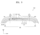
- FIG. 3 is a cross-sectional view taken along line I-I in FIG. 1
- FIG. 4 is a plan view showing an embodiment of a rear surface of a module formed by coupling a light blocking member 330, a buffering member 340, and a curved buffering member 350 in FIG. 3 .
- the window member 100, the bracket 500, and the rear case 600 are omitted in FIG. 3 .
- the cover panel 300 includes the buffering member 340 and the curved buffering member 350.
- the buffering member 340 faces the display surface of the display panel 200 such that the rear surface of the display panel 200 is between the buffering member 340 and the display surface of the display panel 200.
- the buffering member 340 overlaps the flat portion FA.
- the buffering member 340 has an area smaller than that of the flat portion FA when viewed in a plan view. Thus the buffering member 340 is covered by the flat portion FA.
- the buffering member 340 has a first thickness T1.
- the buffering member 340 absorbs part of the impact on the flat portion of the display panel 200 and the flat portion of the window member 100. Thus, the buffering member 340 may reduce or prevent damage to the display panel 200 and the window member 100.
- the buffering member 340 may be formed of, for example, a polymer resin, e.g., polyurethane, polycarbonate, polypropylene, polyethylene, etc., or may be formed from a rubber solution, a urethane-based material, or a sponge obtained, for example, by foaming/molding an acrylic-based material.
- the curved buffering member 350 is on the same layer as the buffering member 340.
- the curved buffering member 350 overlaps the curved portions BA1 and BA2.
- the curved buffering member 350 has an area greater than that of the curved portions BA1 and BA2 when viewed in a plan view to cover the curved portions BA1 and BA2.
- the curved buffering member 350 has a second thickness T2 greater than the first thickness T1.
- the second thickness T2 is one and half times greater than the first thickness T1.
- the curved buffering member 350 may be formed of, for example, a polymer resin, e.g., polyurethane, polycarbonate, polypropylene, polyethylene, etc., or may be formed from a rubber solution, a urethane-based material, or a sponge obtained, for example, by foaming/molding an acrylic-based material.
- a polymer resin e.g., polyurethane, polycarbonate, polypropylene, polyethylene, etc.
- a rubber solution e.g., a urethane-based material, or a sponge obtained, for example, by foaming/molding an acrylic-based material.
- the curved buffering member 350 absorbs part of the impact on the curved portion of the display panel 200 and the curved portion of the window member 100. Thus, the curved buffering member 350 may reduce or prevent damage to the display panel 200 and the window member 100 from external impact.
- the curved portion of the window member 100 may be more vulnerable to impact than the flat portion of the window member 100, since the curved portion of the window member 100 may receive greater stress than applied to the flat portion of the window member 100.
- the curved portion of the display panel 200 may be more vulnerable to impact than the flat portion of the display panel 200, since the curved portion of the display panel 200 may receive greater stress than applied to the flat portion of the display panel 200.
- pixels in the curved portion of the display panel 200 may receive greater stress than applied to pixels in the flat portion of the display panel 200.
- the pixels in the curved portion of the display panel 200 may not properly display images, e.g., images displayed using the pixels in the curved portion of the display panel 200 may be perceived as including a white spot or a black spot.
- the curved buffering member 350 has a thickness greater than the buffering member 340.
- the impact resistance of the curved portions BA1 and BA2 may be improved.
- images displayed using pixels in the curved portions BA1 and BA2 may be prevented from being perceived as including a white or black spot.
- differences in impact resistance between the flat portion FA and the curved portions BA1 and BA2 may be reduced.
- the curved buffering member 350 includes a first curved buffering member 351 and a second curved buffering member 353.
- the first and second curved buffering members 351 and 353 face each other, with the buffering member 340 between the first and second curved buffering members 351 and 353.
- Each of the first and second curved buffering members 351 and 353 may have, for example, substantially a rectangular shape extending in the second direction DR2.
- the first curved buffering member 351 covers the first curved portion BA1 of the display panel 200.
- the first curved buffering member 351 covers a first portion P1 of the flat portion FA, which is connected to the first curved portion BA1.
- the second curved buffering member 353 covers the second curved portion BA2 of the display panel 200.
- the second curved buffering member 353 covers a second portion P2 of the flat portion FA, which is connected to the second curved portion BA2.
- the cover panel 300 may include a light blocking member 330 between the display panel 200 and the buffering member 340 and between the display panel 200 and the curved buffering member 350.
- the light blocking member 330 is attached to the rear surface of the display panel 200 to block the light incident on the display panel 200.
- the light blocking member 330 absorbs or reflects the incident light.
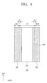
- FIG. 5 is a cross-sectional view taken along a line II-II' of FIG. 1
- FIG. 6 is a plan view showing an embodiment of a rear surface of a module formed by coupling the light blocking member 330, the buffering member 340, the curved buffering member 350, and a heat discharge member 310 in FIG. 3 .
- the cover panel 300 includes the heat discharge member 310 facing the display panel 200, with the buffering member 340 between the heat discharge member 310 and the display panel 200.
- the heat discharge member 310 is attached to the rear surface of the buffering member 340 to effectively discharge heat generated from the display panel 200.
- the heat discharge member 310 overlaps the flat portion FA and does not overlap the curved portions BA1 and BA2.
- the heat discharge member 310 is covered by the buffering member 340 when viewed in a plan view.
- the heat discharge member 310 has a third thickness T3.
- the sum of the first thickness T1 and the third thickness T3 may be equal to or less than the second thickness T2.
- the sum of the first thickness T1 and the third thickness T3 is equal to the second thickness T2. Accordingly, the display apparatus 1000 may have superior heat discharge properties without realizing increased thickness. Also, the difference in impact resistance between the flat portion FA and curved portions BA1 and BA2 may be reduced.
- the heat discharge member 310 includes a heat discharge adhesive layer 311, a graphite layer 313, a protective layer 315, and a blocking layer 317.
- the heat discharge adhesive layer 311 is between and attached the buffering member 340 and the graphite layer 313.
- the heat discharge adhesive layer 311 may include an optical clear adhesive (OCA) or an optical clear resin (OCR).
- the graphite layer 313 includes graphite molecules which have a plate structure in which carbon atoms are connected to each other in a horizontal direction. Therefore, heat conductivity in the horizontal direction of the graphite layer 313 is higher than heat conductivity in a vertical direction of the graphite layer 313. Thus, the graphite layer 313 may demonstrate superior heat discharge properties.
- the protective layer 315 faces the heat discharge adhesive layer 311, with the graphite layer 313 between the protective layer 315 and the heat discharge adhesive layer 311.
- the protective layer 315 prevents the graphite molecules of the graphite layer 313 from blowing.
- the protective layer 315 may include, for example, polyethylene terephthalate (PET).
- the blocking layer 317 is on the buffering member 340, which covers a portion of side surface of the graphite layer 313 along a direction substantially parallel to an upper or rear surface of the graphite layer 313.
- the blocking layer 317 covers the side surface of the graphite layer 313 in the second direction DR2 and exposes the side surface of the graphite layer 313 in the first direction DR1.
- the blocking layer 317 may include, for example, polyethylene terephthalate (PET).
- the heat discharge member 310 may have, for example, a quadrangular shape.
- the heat discharge member 310 includes first, second, third, and fourth sides SD1, SD2, SD3, and SD4.
- the first and second sides SD1 and SD2 are substantially parallel to and face each other, and extend in the first direction DR1.
- the third and fourth sides SD3 and SD4 are substantially parallel to and face each other, and extend in the second direction DR2.
- the blocking layer 317 includes a first blocking layer 317A and a second blocking layer 317B.
- the first blocking layer 317A extends along the first side SD1 and the second blocking layer 317B extends along the second side SD2.
- the first and second blocking layers 317A and 317B face each other in the second direction DR2.
- the heat discharge adhesive layer 311, the graphite layer 313, and the protective layer 315 are between the first and second blocking layers 317A and 317B.
- the cover panel 300 may include an emission member 320 facing the display panel 200, with the buffering member 340 and the curved buffering member 350 between the emission member 320 and display panel 200.
- the emission member 320 is attached to the rear surface of the heat discharge member 310 and the curved buffering member 350.
- the emission member 320 blocks electro-magnetic interference generated from the printed circuit board PCB (refer, e.g., to FIG. 2 ).
- the emission member 320 may discharge heat generated from the display panel 200 together with the heat discharge member 310.
- the emission member 320 includes one or more materials having superior heat conductivity and which block the electro-magnetic interference. Copper, nickel, and ferrite are examples of these materials.
- the emission member 320 may be attached to the heat discharge member 310 and the bracket 500 (refer, e.g., to FIG. 2 ).
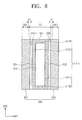
- FIG. 7 is a cross-sectional view showing another embodiment of a display apparatus 1001 taken along a line I-I' in FIG. 1
- FIG. 8 illustrates an embodiment of a rear surface of a module formed by coupling a light blocking member 330, a buffering member 340, a curved buffering member 350, and a heat discharge member 310-1 in FIG. 7 .
- the display apparatus 1001 in FIGS. 7 and 8 have the same structure and function as those of the display apparatus 1000 in FIGS. 3 , 5 , and 6 , except for the heat discharge member 310-1.
- the heat discharge member 310-1 includes a heat discharge adhesive layer 311, a graphite layer 313, a protective layer 315, and a blocking layer 317-1.
- the heat discharge adhesive layer 311, the graphite layer 313, and the protective layer 315 have the same structure and function as in FIGS. 3 , 5 , and 6 .
- the blocking layer 317-1 is on the buffering member 340 and covers the side surface of the graphite layer 313 along a direction substantially parallel to an upper or rear surface of the graphite layer 313. In FIGS. 7 and 8 , the blocking layer 317-1 covers the side surface of the graphite layer 313 in the first and second directions DR1 and DR2.
- the blocking layer 317-1 may include, for example, polyethylene terephthalate (PET).
- the blocking layer 317-1 includes first, second, third, and fourth blocking layers 317A, 317B, 317C, and 317D.
- the first blocking layer 317A extends along the first side SD1 and the second blocking layer 317B extends along the second side SD2.
- the first and second blocking layers 317A and 317B face each other in the second direction DR2, with the heat discharge adhesive layer 311, the graphite layer 313, and the protective layer 315 between the first and second blocking layers 317A and 317B.
- the third blocking layer 317C extends along the third side SD3 and the fourth blocking layer 317D extends along the fourth side SD4.
- the third and fourth blocking layers 317C and 317D face each other in the first direction DR2, with the heat discharge adhesive layer 311, the graphite layer 313, and the protective layer 315 between the third and fourth blocking layers 317C and 317D.
- FIG. 9 is a cross-sectional view of another embodiment of a display apparatus 1002 taken along line I-I' in FIG. 1 .
- the display apparatus 1002 has the same structure and function as the display apparatus 1000 in FIG. 3 , except that the display apparatus 1002 does not include the heat discharge member 310 and the emission member 320.
- the flat portion FA is slimmer and impact resistance of the curved portions BA1 and BA2 is improved.
Landscapes
- Physics & Mathematics (AREA)
- Engineering & Computer Science (AREA)
- Nonlinear Science (AREA)
- General Physics & Mathematics (AREA)
- Computer Hardware Design (AREA)
- Theoretical Computer Science (AREA)
- Optics & Photonics (AREA)
- Mathematical Physics (AREA)
- Chemical & Material Sciences (AREA)
- Crystallography & Structural Chemistry (AREA)
- General Engineering & Computer Science (AREA)
- Human Computer Interaction (AREA)
- Signal Processing (AREA)
- Health & Medical Sciences (AREA)
- Life Sciences & Earth Sciences (AREA)
- Biodiversity & Conservation Biology (AREA)
- Ecology (AREA)
- Environmental & Geological Engineering (AREA)
- Environmental Sciences (AREA)
- Toxicology (AREA)
- Manufacturing & Machinery (AREA)
- Devices For Indicating Variable Information By Combining Individual Elements (AREA)
- Electroluminescent Light Sources (AREA)
Abstract
Description
- One or more embodiments of the invention described herein relate to a display apparatus and a portable terminal.
- Portable terminals usually have display panels for displaying images. A window member may also be included for controlling the appearance of the terminal. The display panels and window members have traditionally had a square or cube shape. Recently, curved display panels and window members have been developed. Curved display panels and window members have been shown to be especially vulnerable to damage from external impact.
- The present invention sets out to provide a display panel that is less vulnerable to damage than prior art devices.
- In accordance with one or more embodiments of the invention, a display apparatus includes a display panel including a curved portion connected to a flat portion; a buffer overlapping the flat portion and having a first thickness; and a curved buffer on a same layer as the buffer and overlapping the curved portion, the curved buffer having a second thickness greater than the first thickness. The curved portion may include a first curved portion facing a second curved portion, and the flat portion may be between the first and second curved portions.
- The first curved portion may be substantially parallel to the second curved portion, and the curved buffer may include a first curved buffer overlapping the first curved portion and a second curved buffer overlapping the second curved portion. The first curved buffer may overlap the first curved portion and a first portion of the flat portion connected to the first curved portion, and the second curved buffer may overlap the second curved portion and a second portion of the flat portion connected to the second curved portion. The second thickness may be substantially one and half times greater than the first thickness.
- The display apparatus may include a light blocking layer between the display panel and the buffer and between the display panel and the curved buffer. The display apparatus include a heat discharge layer facing the display panel, wherein the buffer may be between the heat discharge layer and the display panel. The heat discharge layer may overlap the flat portion and does not overlap the curved portion.
- The heat discharge layer may have a third thickness, and a sum of the first thickness and the third thickness may be substantially equal to or less than the second thickness. The curved portion may be adjacent to the flat portion in a first direction and extends in a second direction crossing the first direction, and the heat discharge layer may include a graphite layer; a heat discharge adhesive layer between and to attach the buffer and the graphite layer; a protective layer facing the heat discharge adhesive layer, with the graphite layer between the heat discharge adhesive layer and the protective layer; and a blocking layer overlapping a portion of a side surface of the graphite layer in the first direction or the second direction.
- The heat discharge layer may include a first side extending in the first direction, a second side substantially parallel to the first side, a third side extending in the second direction, and a fourth side substantially parallel to the third side, and the blocking layer may include a first blocking layer extending along the first side and a second blocking layer extending along the second side. The first and second blocking layers may face each other in the second direction, and the heat discharge adhesive layer, the graphite layer, and the protective layer may be between the first and second blocking layers.
- The blocking layer may include a third blocking layer extending along the third side; and a fourth blocking layer extending along the fourth side. The third and fourth blocking layers may face each other in the first direction, and the heat discharge adhesive layer, the graphite layer, and the protective layer may be between the third and fourth blocking layers. The display apparatus may include an emission layer facing the display panel, wherein the buffer and the curved buffer may be between the emission layer and the display panel. The emission layer may be attached to the curved buffer.
- In accordance with one or more other embodiments of the invention, a portable terminal includes a display panel including a curved portion connected to a flat portion; a buffer overlapping the flat portion and having a first thickness; and a curved buffer on a same layer as the buffer and overlapping the curved portion, the curved buffer having a second thickness greater than the first thickness. The portable terminal may include a light blocking layer between the display panel and the buffer and between the display panel and the curved buffer; a heat discharge layer overlapping the flat portion, not overlapping the curved portion, and facing the display panel, wherein the buffer is between the heat discharge layer and the display panel; and an emission layer facing the display panel, wherein the buffer and the curved buffer are between the emission layer and the display panel and are attached to the curved buffer and the heat discharge layer. The portable terminal may include a window above the display panel; and a bracket facing the display panel, wherein the buffer and the curved buffer are between the bracket and the display panel. The display panel may be an organic light emitting display panel.
- At least some of the above and other features of the invention are set out in the claims.
- Features of the invention will be made more apparent to those of skill in the art by describing in detail embodiments of the invention with reference to the attached drawings in which:
-
FIG. 1 illustrates an embodiment of a display apparatus; -
FIG. 2 illustrates another view of the display apparatus; -
FIG. 3 illustrates a view along section line I-I inFIG. 1 ; -
FIG. 4 illustrates the rear surface of an embodiment of a module; -
FIG. 5 illustrates a view along section line II-II' inFIG. 1 ; -
FIG. 6 illustrates the rear surface of another embodiment of a module; -
FIG. 7 illustrates another embodiment of a display apparatus; -
FIG. 8 illustrates the rear surface of another embodiment of a module; and -
FIG. 9 illustrates another embodiment of a display apparatus. - Example embodiments of the invention are described more fully hereinafter with reference to the accompanying drawings; however, it may be embodied in different forms and should not be construed as limited to the embodiments set forth herein. Rather, these embodiments are provided so that this disclosure will be thorough, and will convey implementations to those skilled in the art. The embodiments may be combined to form additional embodiments.
- It will also be understood that when a layer or element is referred to as being "on" another layer or substrate, it can be directly on the other layer or substrate, or intervening layers may also be present. Further, it will be understood that when a layer is referred to as being "under" another layer, it can be directly under, and one or more intervening layers may also be present. In addition, it will also be understood that when a layer is referred to as being "between" two layers, it can be the only layer between the two layers, or one or more intervening layers may also be present. Like reference numerals refer to like elements throughout.
-
FIG. 1 illustrates an embodiment of adisplay apparatus 1000 according to the invention, andFIG. 2 illustrates an exploded perspective view of thedisplay apparatus 1000. Thedisplay apparatus 1000 may be included, for example, in a portable terminal. The portable terminal may be, for example, a personal computer (PC), a tablet PC, a notebook computer, a navigation unit, a camera, a mobile telephone, a personal digital assistant (PDA), a portable multimedia player (PMP), a game unit, or a wrist-type electronic device. Thedisplay apparatus 1000 may also be applied to a large-sized electronic item such as but not limited to a television set or an outdoor billboard. - As shown in
FIG. 1 , thedisplay apparatus 1000 includes a plurality of areas defined on a display surface. Thedisplay apparatus 1000 includes a display area AR through which images IM1 and IM2 are displayed and a non-display area BR adjacent to the display area AR. The display area AR may have, for example, substantially a quadrangular shape or another shape. The non-display area BR surrounds the display area AR. - The
display apparatus 1000 may have a curved portion. For example, thedisplay apparatus 1000 may include a flat portion FA and curved portions adjacent to the flat portion FA. The flat portion FA is substantially parallel to a surface defined by a first direction DR1 and a second direction DR2 and a normal line of the flat portion FA corresponds to a third direction DR3. The third direction DR3 may be, for example, a reference direction for distinguishing a front surface from a rear surface. - The curved portions include a first curved portion BA1 and a second curved portion BA2. The first and second curved portions BA1 and BA2 are spaced from each other in the first direction DR1, and the flat portion FA is between the first and second curved portions BA1 and BA2. The first and second curved portions BA1 and BA2 extend in the second direction DR2. The embodiment of
FIG. 1 has two curved portions BA1 and BA2. In another embodiment, one curved portion (e.g., only one of the first or second curved portions BA1 and BA2) or more than two curved portions may be included. - The display area AR has one portion disposed in the flat portion FA and other portions in the curved portions BA1 and BA2. The flat portion FA displays a first image IM1 and the curved portions BA1 and BA2 display second and third images IM2 and IM3, respectively. For illustrative purposes only,
FIG. 1 shows that the first image IM1 includes an internet search window. The second and third images IM2 and IM3 may include various icons, images, and/or other information. In another embodiment, only one curved portion may be exist. - Referring to
FIGS. 1 and2 , thedisplay apparatus 1000 includes awindow member 100, adisplay panel 200, acover panel 300, abracket 500, and arear case 600. In one embodiment, each of thewindow member 100, thedisplay panel 200, thecover panel 300, and thebracket 500 may have a partially curved shape. For example, each of thewindow member 100, thedisplay panel 200, thecover panel 300, and thebracket 500 may include a flat portion and at least one curved portion. The flat portion of each of thewindow member 100, thedisplay panel 200, thecover panel 300, and thebracket 500 may correspond to the flat portion FA of thedisplay apparatus 1000. The at least one curved portion of each of thewindow member 100, thedisplay panel 200, thecover panel 300, and thebracket 500 may correspond to the curved portions BA1 and BA2 of thedisplay apparatus 1000. - For the convenience of explanation, the flat portion FA and the curved portions BA1 and BA2 may be used to indicate the flat portion and the curved portion of each of the
window member 100, thedisplay panel 200, thecover panel 300, and thebracket 500. For instance, the flat portion of thedisplay panel 200 may indicate a portion of thedisplay panel 200, which forms the flat portion FA. - The
window member 100 includes a display area 100-AR for transmitting the images IM1 and IM2 from thedisplay panel 200 and a non-display area 100-BR adjacent to the display area 100-AR. Thewindow member 100 is above thedisplay panel 200. Thewindow member 100 may include a cover window made of, for example, glass, sapphire, or plastic. - The
display panel 200 includes a display area 200-AR and a non-display area 200-BR. The display area 200-AR displays the images IM1 and IM2 and corresponds to the display area 100-AR of thewindow member 100. The non-display area 200-BR is adjacent to the display area 200-AR and corresponds to the non-display area 100-BR of thewindow member 100. - The
display panel 200 may be, for example, an organic light emitting display panel. In this case, thedisplay panel 200 includes asubstrate 210, an organic light emitting diode, and asealing layer 220. The organic light emitting diode is on thesubstrate 210. Thesealing layer 220 is on thesubstrate 210 and seals the organic light emitting diode from the outside environment. - The organic light emitting diode includes a first electrode, an organic light emitting layer, and a second electrode. The first electrode is an anode electrode or a positive electrode. The second electrode is a cathode electrode or a negative electrode. The first electrode generates holes and the second electrode generates electrons. The holes generated by the first electrode and electrons generated by the second electrode are injected into the organic light emitting layer. The holes and electrons injected into the organic light emitting layer are recombined in the organic light emitting layer to generate excitons. Light is emitted when the excitons transition to a ground state from an excited state.
- The
display panel 200 includes a display surface on which the images IM1 and IM2 are displayed and a rear surface opposite to the display surface. InFIG. 2 , the display surface corresponds to an upper surface of thesealing layer 220 and the rear surface corresponds to a lower surface of thesubstrate 210. - The
display apparatus 1000 may further include a flexible printed circuit board FPCB and a printed circuit board PCB. The flexible printed circuit board FPCB electrically connects thedisplay panel 200 and the printed circuit board PCB. One end of the flexible printed circuit board FPCB is connected to one surface of thesubstrate 210, which is not covered by thesealing layer 220. The other end of the flexible printed circuit board FPCB is connected to the printed circuit board PCB. The flexible printed circuit board FPCB has flexibility. Thus, the flexible printed circuit board FPCB is bent to a lower side of thecover panel 300 while being coupled to the printed circuit board PCB. - The printed circuit board PCB applies signals to or receives signals from the
display panel 200 through the flexible printed circuit board FPCB. The printed circuit board PCB is attached to the lower side of thecover panel 300 due to bending of the flexible printed circuit board FPCB. The printed circuit board PCB may be connected to a connector CB to receive a signal from an external source. - The
display apparatus 1000 may include a touch panel between thewindow member 100 and thedisplay panel 200. The touch panel may be, for example, inside thedisplay panel 200. The touch panel may be a resistive type touch panel, an electrostatic capacitive type touch panel, or an electromagnetic induction type touch panel and operates to obtain coordinate information corresponding to a touch position. - The
cover panel 300 is attached to the rear surface of thedisplay panel 200, and is between thedisplay panel 200 and the printed circuit board PCB when coupled together. - The
bracket 500 supports thedisplay panel 200 and thecover panel 300. One surface of thebracket 500 is attached to thecover panel 300 and electronic components are mounted on the other surface of thebracket 500. - The
rear case 600 is coupled to thewindow member 100 to accommodate thedisplay panel 200 andcover panel 300. Therear case 600 is made of, for example, a plastic or metallic material. Therear case 600 may be omitted in another embodiment. -
FIG. 3 is a cross-sectional view taken along line I-I inFIG. 1 , andFIG. 4 is a plan view showing an embodiment of a rear surface of a module formed by coupling alight blocking member 330, a bufferingmember 340, and acurved buffering member 350 inFIG. 3 . For the convenience of explanation, thewindow member 100, thebracket 500, and therear case 600 are omitted inFIG. 3 . - Referring to
FIGS. 2 to 4 , thecover panel 300 includes the bufferingmember 340 and thecurved buffering member 350. The bufferingmember 340 faces the display surface of thedisplay panel 200 such that the rear surface of thedisplay panel 200 is between the bufferingmember 340 and the display surface of thedisplay panel 200. The bufferingmember 340 overlaps the flat portion FA. The bufferingmember 340 has an area smaller than that of the flat portion FA when viewed in a plan view. Thus the bufferingmember 340 is covered by the flat portion FA. The bufferingmember 340 has a first thickness T1. - The buffering
member 340 absorbs part of the impact on the flat portion of thedisplay panel 200 and the flat portion of thewindow member 100. Thus, the bufferingmember 340 may reduce or prevent damage to thedisplay panel 200 and thewindow member 100. The bufferingmember 340 may be formed of, for example, a polymer resin, e.g., polyurethane, polycarbonate, polypropylene, polyethylene, etc., or may be formed from a rubber solution, a urethane-based material, or a sponge obtained, for example, by foaming/molding an acrylic-based material. - The
curved buffering member 350 is on the same layer as the bufferingmember 340. Thecurved buffering member 350 overlaps the curved portions BA1 and BA2. Thecurved buffering member 350 has an area greater than that of the curved portions BA1 and BA2 when viewed in a plan view to cover the curved portions BA1 and BA2. Thecurved buffering member 350 has a second thickness T2 greater than the first thickness T1. In one embodiment, the second thickness T2 is one and half times greater than the first thickness T1. When T2 > T1, and especially when T2 = 1.5T1, the thickness of thedisplay apparatus 1000 may be reduced and impact resistance of the flat portion FA and the curved portions BA1 and BA2 may be improved. - The
curved buffering member 350 may be formed of, for example, a polymer resin, e.g., polyurethane, polycarbonate, polypropylene, polyethylene, etc., or may be formed from a rubber solution, a urethane-based material, or a sponge obtained, for example, by foaming/molding an acrylic-based material. - The
curved buffering member 350 absorbs part of the impact on the curved portion of thedisplay panel 200 and the curved portion of thewindow member 100. Thus, thecurved buffering member 350 may reduce or prevent damage to thedisplay panel 200 and thewindow member 100 from external impact. - The curved portion of the
window member 100 may be more vulnerable to impact than the flat portion of thewindow member 100, since the curved portion of thewindow member 100 may receive greater stress than applied to the flat portion of thewindow member 100. - Similarly, the curved portion of the
display panel 200 may be more vulnerable to impact than the flat portion of thedisplay panel 200, since the curved portion of thedisplay panel 200 may receive greater stress than applied to the flat portion of thedisplay panel 200. In addition, pixels in the curved portion of thedisplay panel 200 may receive greater stress than applied to pixels in the flat portion of thedisplay panel 200. As a result, the pixels in the curved portion of thedisplay panel 200 may not properly display images, e.g., images displayed using the pixels in the curved portion of thedisplay panel 200 may be perceived as including a white spot or a black spot. - In the
display apparatus 1000, thecurved buffering member 350 has a thickness greater than the bufferingmember 340. Thus, the impact resistance of the curved portions BA1 and BA2 may be improved. In addition, images displayed using pixels in the curved portions BA1 and BA2 may be prevented from being perceived as including a white or black spot. Further, differences in impact resistance between the flat portion FA and the curved portions BA1 and BA2 may be reduced. - The
curved buffering member 350 includes a firstcurved buffering member 351 and a secondcurved buffering member 353. The first and secondcurved buffering members member 340 between the first and secondcurved buffering members curved buffering members - The first
curved buffering member 351 covers the first curved portion BA1 of thedisplay panel 200. The firstcurved buffering member 351 covers a first portion P1 of the flat portion FA, which is connected to the first curved portion BA1. The secondcurved buffering member 353 covers the second curved portion BA2 of thedisplay panel 200. The secondcurved buffering member 353 covers a second portion P2 of the flat portion FA, which is connected to the second curved portion BA2. - The
cover panel 300 may include alight blocking member 330 between thedisplay panel 200 and thebuffering member 340 and between thedisplay panel 200 and thecurved buffering member 350. Thelight blocking member 330 is attached to the rear surface of thedisplay panel 200 to block the light incident on thedisplay panel 200. Thelight blocking member 330 absorbs or reflects the incident light. -
FIG. 5 is a cross-sectional view taken along a line II-II' ofFIG. 1 , andFIG. 6 is a plan view showing an embodiment of a rear surface of a module formed by coupling thelight blocking member 330, the bufferingmember 340, thecurved buffering member 350, and aheat discharge member 310 inFIG. 3 . - Referring to
FIGS. 3 ,5 , and6 , thecover panel 300 includes theheat discharge member 310 facing thedisplay panel 200, with the bufferingmember 340 between theheat discharge member 310 and thedisplay panel 200. Theheat discharge member 310 is attached to the rear surface of the bufferingmember 340 to effectively discharge heat generated from thedisplay panel 200. - The
heat discharge member 310 overlaps the flat portion FA and does not overlap the curved portions BA1 and BA2. Theheat discharge member 310 is covered by the bufferingmember 340 when viewed in a plan view. Theheat discharge member 310 has a third thickness T3. In one embodiment, the sum of the first thickness T1 and the third thickness T3 may be equal to or less than the second thickness T2. InFIG. 3 , the sum of the first thickness T1 and the third thickness T3 is equal to the second thickness T2. Accordingly, thedisplay apparatus 1000 may have superior heat discharge properties without realizing increased thickness. Also, the difference in impact resistance between the flat portion FA and curved portions BA1 and BA2 may be reduced. - The
heat discharge member 310 includes a heatdischarge adhesive layer 311, agraphite layer 313, aprotective layer 315, and ablocking layer 317. The heatdischarge adhesive layer 311 is between and attached the bufferingmember 340 and thegraphite layer 313. The heatdischarge adhesive layer 311 may include an optical clear adhesive (OCA) or an optical clear resin (OCR). - The
graphite layer 313 includes graphite molecules which have a plate structure in which carbon atoms are connected to each other in a horizontal direction. Therefore, heat conductivity in the horizontal direction of thegraphite layer 313 is higher than heat conductivity in a vertical direction of thegraphite layer 313. Thus, thegraphite layer 313 may demonstrate superior heat discharge properties. - The
protective layer 315 faces the heatdischarge adhesive layer 311, with thegraphite layer 313 between theprotective layer 315 and the heatdischarge adhesive layer 311. Theprotective layer 315 prevents the graphite molecules of thegraphite layer 313 from blowing. Theprotective layer 315 may include, for example, polyethylene terephthalate (PET). - The
blocking layer 317 is on thebuffering member 340, which covers a portion of side surface of thegraphite layer 313 along a direction substantially parallel to an upper or rear surface of thegraphite layer 313. InFIG. 6 , theblocking layer 317 covers the side surface of thegraphite layer 313 in the second direction DR2 and exposes the side surface of thegraphite layer 313 in the first direction DR1. Theblocking layer 317 may include, for example, polyethylene terephthalate (PET). - The
heat discharge member 310 may have, for example, a quadrangular shape. Theheat discharge member 310 includes first, second, third, and fourth sides SD1, SD2, SD3, and SD4. The first and second sides SD1 and SD2 are substantially parallel to and face each other, and extend in the first direction DR1. The third and fourth sides SD3 and SD4 are substantially parallel to and face each other, and extend in the second direction DR2. - The
blocking layer 317 includes afirst blocking layer 317A and asecond blocking layer 317B. Thefirst blocking layer 317A extends along the first side SD1 and thesecond blocking layer 317B extends along the second side SD2. The first and second blocking layers 317A and 317B face each other in the second direction DR2. The heatdischarge adhesive layer 311, thegraphite layer 313, and theprotective layer 315 are between the first and second blocking layers 317A and 317B. - Referring again to
FIGS. 3 and5 , thecover panel 300 may include anemission member 320 facing thedisplay panel 200, with the bufferingmember 340 and thecurved buffering member 350 between theemission member 320 anddisplay panel 200. Theemission member 320 is attached to the rear surface of theheat discharge member 310 and thecurved buffering member 350. Theemission member 320 blocks electro-magnetic interference generated from the printed circuit board PCB (refer, e.g., toFIG. 2 ). In addition, theemission member 320 may discharge heat generated from thedisplay panel 200 together with theheat discharge member 310. - The
emission member 320 includes one or more materials having superior heat conductivity and which block the electro-magnetic interference. Copper, nickel, and ferrite are examples of these materials. Theemission member 320 may be attached to theheat discharge member 310 and the bracket 500 (refer, e.g., toFIG. 2 ). -
FIG. 7 is a cross-sectional view showing another embodiment of adisplay apparatus 1001 taken along a line I-I' inFIG. 1 , andFIG. 8 illustrates an embodiment of a rear surface of a module formed by coupling alight blocking member 330, a bufferingmember 340, acurved buffering member 350, and a heat discharge member 310-1 inFIG. 7 . - The
display apparatus 1001 inFIGS. 7 and8 have the same structure and function as those of thedisplay apparatus 1000 inFIGS. 3 ,5 , and6 , except for the heat discharge member 310-1. The heat discharge member 310-1 includes a heatdischarge adhesive layer 311, agraphite layer 313, aprotective layer 315, and a blocking layer 317-1. The heatdischarge adhesive layer 311, thegraphite layer 313, and theprotective layer 315 have the same structure and function as inFIGS. 3 ,5 , and6 . - The blocking layer 317-1 is on the
buffering member 340 and covers the side surface of thegraphite layer 313 along a direction substantially parallel to an upper or rear surface of thegraphite layer 313. InFIGS. 7 and8 , the blocking layer 317-1 covers the side surface of thegraphite layer 313 in the first and second directions DR1 and DR2. The blocking layer 317-1 may include, for example, polyethylene terephthalate (PET). - The blocking layer 317-1 includes first, second, third, and fourth blocking layers 317A, 317B, 317C, and 317D. The
first blocking layer 317A extends along the first side SD1 and thesecond blocking layer 317B extends along the second side SD2. The first and second blocking layers 317A and 317B face each other in the second direction DR2, with the heatdischarge adhesive layer 311, thegraphite layer 313, and theprotective layer 315 between the first and second blocking layers 317A and 317B. - The
third blocking layer 317C extends along the third side SD3 and thefourth blocking layer 317D extends along the fourth side SD4. The third and fourth blocking layers 317C and 317D face each other in the first direction DR2, with the heatdischarge adhesive layer 311, thegraphite layer 313, and theprotective layer 315 between the third and fourth blocking layers 317C and 317D. -
FIG. 9 is a cross-sectional view of another embodiment of adisplay apparatus 1002 taken along line I-I' inFIG. 1 . Thedisplay apparatus 1002 has the same structure and function as thedisplay apparatus 1000 inFIG. 3 , except that thedisplay apparatus 1002 does not include theheat discharge member 310 and theemission member 320. - Referring to
FIG. 9 , since thedisplay apparatus 1002 does not include theheat discharge member 310 and theemission member 320, the flat portion FA is slimmer and impact resistance of the curved portions BA1 and BA2 is improved. - Example embodiments have been disclosed herein, and although specific terms are employed, they are used and are to be interpreted in a generic and descriptive sense only and not for purpose of limitation. In some instances, as would be apparent to one of skill in the art as of the filing of the present application, features, characteristics, and/or elements described in connection with a particular embodiment may be used singly or in combination with features, characteristics, and/or elements described in connection with other embodiments unless otherwise indicated. Accordingly, it will be understood by those of skill in the art that various changes in form and details may be made without departing from the scope of the invention as set forth in the following claims.
Claims (15)
- A display apparatus, comprising:a display panel including a curved portion connected to a flat portion;a buffer overlapping the flat portion and having a first thickness; anda curved buffer on a same layer as the buffer and overlapping the curved portion, the curved buffer having a second thickness that is greater than the first thickness.
- A display apparatus as claimed in claim 1, wherein:the curved portion includes a first curved portion facing a second curved portion, andthe flat portion is between the first and second curved portions.
- A display apparatus as claimed in claim 2, wherein:the first curved portion is substantially parallel to the second curved portion, andthe curved buffer includes a first curved buffer overlapping the first curved portion and a second curved buffer overlapping the second curved portion.
- A display apparatus as claimed in claim 3, wherein:the first curved buffer overlaps the first curved portion and a first portion of the flat portion connected to the first curved portion, andthe second curved buffer overlaps the second curved portion and a second portion of the flat portion connected to the second curved portion.
- A display apparatus as claimed in any preceding claim, wherein the second thickness is substantially one and a half times greater than the first thickness.
- A display apparatus as claimed in any preceding claim, further comprising:a light blocking layer between the display panel and the buffer and between the display panel and the curved buffer.
- A display apparatus as claimed in any preceding claim, further comprising:a heat discharge layer facing the display panel,wherein the buffer is between the heat discharge layer and the display panel.
- A display apparatus as claimed in claim 7, wherein the heat discharge layer overlaps the flat portion and does not overlap the curved portion.
- A display apparatus as claimed in claim 7, or 8, wherein:the heat discharge layer has a third thickness, anda sum of the first thickness and the third thickness is substantially equal to or less than the second thickness.
- A display apparatus as claimed in claim 7, wherein:the curved portion is adjacent to the flat portion in a first direction and extends in a second direction crossing the first direction, andthe heat discharge layer includes:a graphite layer;a heat discharge adhesive layer between and to attach the buffer and the graphite layer;a protective layer facing the heat discharge adhesive layer, with the graphite layer between the heat discharge adhesive layer and the protective layer; anda blocking layer overlapping a portion of a side surface of the graphite layer in the first direction or the second direction.
- A display apparatus as claimed in claim 10, wherein:the heat discharge layer includes a first side extending in the first direction, a second side substantially parallel to the first side, a third side extending in the second direction, and a fourth side substantially parallel to the third side, andthe blocking layer includes a first blocking layer extending along the first side and a second blocking layer extending along the second side.
- A display apparatus as claimed in claim 11, wherein the first and second blocking layers face each other in the second direction, and wherein the heat discharge adhesive layer, the graphite layer, and the protective layer are between the first and second blocking layers.
- A display apparatus as claimed in claim 11, wherein the blocking layer includes:a third blocking layer extending along the third side; anda fourth blocking layer extending along the fourth side.
- A display apparatus as claimed in claim 13, wherein:the third and fourth blocking layers face each other in the first direction, andthe heat discharge adhesive layer, the graphite layer, and the protective layer are between the third and fourth blocking layers.
- A portable terminal, comprising a display apparatus according to any preceding claim..
Applications Claiming Priority (1)
| Application Number | Priority Date | Filing Date | Title |
|---|---|---|---|
| KR1020150033347A KR102274142B1 (en) | 2015-03-10 | 2015-03-10 | Display apparatus and portable terminal |
Publications (2)
| Publication Number | Publication Date |
|---|---|
| EP3067775A1 true EP3067775A1 (en) | 2016-09-14 |
| EP3067775B1 EP3067775B1 (en) | 2020-01-08 |
Family
ID=55361348
Family Applications (1)
| Application Number | Title | Priority Date | Filing Date |
|---|---|---|---|
| EP16154757.5A Active EP3067775B1 (en) | 2015-03-10 | 2016-02-09 | Display apparatus and portable terminal |
Country Status (5)
| Country | Link |
|---|---|
| US (2) | US9935278B2 (en) |
| EP (1) | EP3067775B1 (en) |
| KR (1) | KR102274142B1 (en) |
| CN (1) | CN105977274B (en) |
| TW (1) | TWI704540B (en) |
Cited By (1)
| Publication number | Priority date | Publication date | Assignee | Title |
|---|---|---|---|---|
| US11526201B2 (en) * | 2019-08-02 | 2022-12-13 | Samsung Display Co., Ltd. | Panel bottom sheet and display including the same |
Families Citing this family (23)
| Publication number | Priority date | Publication date | Assignee | Title |
|---|---|---|---|---|
| KR101719208B1 (en) * | 2015-06-17 | 2017-03-23 | 주식회사 하이딥 | Touch pressure detectable touch input device including display module |
| KR102562895B1 (en) * | 2015-12-15 | 2023-08-04 | 삼성디스플레이 주식회사 | Manufacturing apparatus and method for display apparatus |
| KR102152734B1 (en) * | 2016-11-17 | 2020-09-08 | 삼성디스플레이 주식회사 | Laminate apparatus and method for manufacturing display device |
| US10312228B2 (en) | 2017-01-25 | 2019-06-04 | Innolux Corporation | Display device |
| KR102611125B1 (en) | 2017-02-15 | 2023-12-08 | 삼성전자 주식회사 | Electronic device with curved window |
| CN107221607B (en) | 2017-05-25 | 2019-06-07 | 京东方科技集团股份有限公司 | A kind of encapsulating structure of display device and preparation method thereof, display device |
| KR102367881B1 (en) | 2017-07-03 | 2022-02-25 | 삼성디스플레이 주식회사 | display device |
| KR102398176B1 (en) * | 2017-08-18 | 2022-05-16 | 삼성디스플레이 주식회사 | Display device |
| KR102433103B1 (en) * | 2017-10-02 | 2022-08-17 | 삼성디스플레이 주식회사 | Display device |
| KR102458284B1 (en) * | 2018-05-02 | 2022-10-25 | 삼성디스플레이 주식회사 | Display apparatus and portable terminal |
| KR102582263B1 (en) * | 2018-08-20 | 2023-09-25 | 삼성디스플레이 주식회사 | Display device and method for manufacturing the same |
| KR102519732B1 (en) | 2018-09-19 | 2023-04-11 | 삼성전자주식회사 | Foldable electronic device including integral type adhesive layer and adhesion prevention part |
| KR102645189B1 (en) * | 2018-11-20 | 2024-03-08 | 삼성디스플레이 주식회사 | Display device |
| KR102543720B1 (en) * | 2018-12-13 | 2023-06-13 | 엘지디스플레이 주식회사 | Flexible display module and electronic device comprising the same |
| KR102562204B1 (en) * | 2018-12-13 | 2023-07-31 | 엘지디스플레이 주식회사 | Flexible display module and electronic device comprising the same |
| KR102534189B1 (en) | 2018-12-17 | 2023-05-17 | 엘지디스플레이 주식회사 | Heat radiation member for flexible display and electronic device using the same |
| KR102832101B1 (en) * | 2019-08-02 | 2025-07-09 | 삼성디스플레이 주식회사 | Display device |
| US11570938B2 (en) * | 2019-08-27 | 2023-01-31 | Lg Display Co., Ltd. | Display device |
| US11468832B2 (en) | 2019-11-08 | 2022-10-11 | Beijing Boe Technology Development Co., Ltd. | Array substrate and method for manufacturing same, display panel, and display device |
| CN113439295B (en) * | 2019-11-28 | 2024-09-03 | 京东方科技集团股份有限公司 | Display module and manufacturing method thereof, and display device |
| KR102794841B1 (en) * | 2020-01-10 | 2025-04-14 | 삼성전자주식회사 | An electronic device comprising a housing |
| CN111768707B (en) * | 2020-06-30 | 2022-03-11 | 上海天马微电子有限公司 | Flexible display panel and display device |
| KR20230030692A (en) * | 2021-08-25 | 2023-03-07 | 삼성디스플레이 주식회사 | Panel bottom sheet and display device comprising the same |
Citations (2)
| Publication number | Priority date | Publication date | Assignee | Title |
|---|---|---|---|---|
| US20140168090A1 (en) * | 2012-12-13 | 2014-06-19 | Nokia Corporation | Display apparatus and associated method |
| US20150029661A1 (en) * | 2014-10-15 | 2015-01-29 | AzTrong Inc. | Wearable portable electronic device with heat conducting path |
Family Cites Families (20)
| Publication number | Priority date | Publication date | Assignee | Title |
|---|---|---|---|---|
| KR101484944B1 (en) * | 2008-10-02 | 2015-01-22 | 삼성전자 주식회사 | Electronic device case and manufacturing method thereof |
| US20100253902A1 (en) * | 2009-04-07 | 2010-10-07 | Semiconductor Energy Laboratory Co., Ltd. | Liquid crystal display device and manufacturing method thereof |
| DE112010001807T5 (en) * | 2009-04-30 | 2012-06-21 | Mitsubishi Electric Corporation | Display device and method for its production |
| CN102473363B (en) * | 2009-07-01 | 2014-08-27 | 夏普株式会社 | Display device |
| KR101394936B1 (en) * | 2009-11-06 | 2014-05-14 | 엘지디스플레이 주식회사 | Flat plate display device with light shilding layer |
| KR101320384B1 (en) * | 2011-06-30 | 2013-10-23 | 삼성디스플레이 주식회사 | Flexible display panel and the display apparatus comprising the flexible display panel |
| KR101190630B1 (en) * | 2012-01-30 | 2012-10-15 | 주식회사 지앤씨에스 | Organic light emitting diode display |
| US8947866B2 (en) | 2012-06-21 | 2015-02-03 | Corning Incorporated | Edge armored display cover plate |
| KR20140002470A (en) | 2012-06-29 | 2014-01-08 | 삼성디스플레이 주식회사 | Display device, manufacturing method of the same and manufacturing device of the same |
| KR20140046839A (en) | 2012-10-11 | 2014-04-21 | 삼성디스플레이 주식회사 | Flexible display device |
| KR101996437B1 (en) * | 2012-10-16 | 2019-07-05 | 삼성디스플레이 주식회사 | Transparent protection window, flexible display apparatus with the same and the method for manufacturing the transparent protection window |
| KR102117890B1 (en) * | 2012-12-28 | 2020-06-02 | 엘지디스플레이 주식회사 | Flexible display device and method for manufacturing the same |
| KR102053411B1 (en) * | 2013-03-07 | 2019-12-09 | 삼성디스플레이 주식회사 | Organic light emitting diode display |
| KR20140128721A (en) | 2013-04-29 | 2014-11-06 | 삼성디스플레이 주식회사 | Display device and method of manufacturing a display device |
| KR102055281B1 (en) * | 2013-05-21 | 2019-12-13 | 삼성디스플레이 주식회사 | Display apparatus |
| KR20140141330A (en) | 2013-05-31 | 2014-12-10 | 삼성디스플레이 주식회사 | Organic light emitting display moduled and display device having the same |
| US20140370222A1 (en) * | 2013-06-18 | 2014-12-18 | A-Tech Solution Co., Ltd | Heat-dissipation sheet assembly manufactured by using electrochemical method |
| KR102118578B1 (en) * | 2013-10-17 | 2020-06-04 | 삼성디스플레이 주식회사 | Organic light emitting diode display |
| TWI531940B (en) * | 2014-05-08 | 2016-05-01 | 群創光電股份有限公司 | Curved touch-controlled display device and manufacturing method thereof |
| FR3021134B1 (en) * | 2014-05-14 | 2023-01-06 | Lg Electronics Inc | MOBILE TERMINAL |
-
2015
- 2015-03-10 KR KR1020150033347A patent/KR102274142B1/en active Active
- 2015-11-09 US US14/935,475 patent/US9935278B2/en active Active
-
2016
- 2016-01-27 TW TW105102488A patent/TWI704540B/en active
- 2016-02-09 EP EP16154757.5A patent/EP3067775B1/en active Active
- 2016-02-16 CN CN201610086618.3A patent/CN105977274B/en active Active
-
2018
- 2018-02-28 US US15/907,555 patent/US10276810B2/en active Active
Patent Citations (2)
| Publication number | Priority date | Publication date | Assignee | Title |
|---|---|---|---|---|
| US20140168090A1 (en) * | 2012-12-13 | 2014-06-19 | Nokia Corporation | Display apparatus and associated method |
| US20150029661A1 (en) * | 2014-10-15 | 2015-01-29 | AzTrong Inc. | Wearable portable electronic device with heat conducting path |
Cited By (2)
| Publication number | Priority date | Publication date | Assignee | Title |
|---|---|---|---|---|
| US11526201B2 (en) * | 2019-08-02 | 2022-12-13 | Samsung Display Co., Ltd. | Panel bottom sheet and display including the same |
| US11953958B2 (en) | 2019-08-02 | 2024-04-09 | Samsung Display Co., Ltd. | Panel bottom sheet and display including the same |
Also Published As
| Publication number | Publication date |
|---|---|
| EP3067775B1 (en) | 2020-01-08 |
| KR20160110674A (en) | 2016-09-22 |
| US9935278B2 (en) | 2018-04-03 |
| KR102274142B1 (en) | 2021-07-09 |
| US10276810B2 (en) | 2019-04-30 |
| TW201633272A (en) | 2016-09-16 |
| CN105977274A (en) | 2016-09-28 |
| TWI704540B (en) | 2020-09-11 |
| US20160268523A1 (en) | 2016-09-15 |
| CN105977274B (en) | 2021-08-03 |
| US20180190916A1 (en) | 2018-07-05 |
Similar Documents
| Publication | Publication Date | Title |
|---|---|---|
| EP3067775B1 (en) | Display apparatus and portable terminal | |
| EP3067776B1 (en) | Display apparatus and portable terminal | |
| US12101956B2 (en) | Display device | |
| US10091884B2 (en) | Display device with a reinforcing member for improved durability | |
| US10842033B2 (en) | Display device and portable terminal | |
| KR102420438B1 (en) | Display apparatus and portable terminal | |
| CN102855821B (en) | Flexible display panel and display apparatus including the flexible display panel | |
| US20200381638A1 (en) | Display device | |
| KR102709999B1 (en) | Display Device | |
| CN121510827A (en) | Display device and electronic device including the display device |
Legal Events
| Date | Code | Title | Description |
|---|---|---|---|
| PUAI | Public reference made under article 153(3) epc to a published international application that has entered the european phase |
Free format text: ORIGINAL CODE: 0009012 |
|
| AK | Designated contracting states |
Kind code of ref document: A1 Designated state(s): AL AT BE BG CH CY CZ DE DK EE ES FI FR GB GR HR HU IE IS IT LI LT LU LV MC MK MT NL NO PL PT RO RS SE SI SK SM TR |
|
| AX | Request for extension of the european patent |
Extension state: BA ME |
|
| STAA | Information on the status of an ep patent application or granted ep patent |
Free format text: STATUS: REQUEST FOR EXAMINATION WAS MADE |
|
| 17P | Request for examination filed |
Effective date: 20170313 |
|
| RBV | Designated contracting states (corrected) |
Designated state(s): AL AT BE BG CH CY CZ DE DK EE ES FI FR GB GR HR HU IE IS IT LI LT LU LV MC MK MT NL NO PL PT RO RS SE SI SK SM TR |
|
| STAA | Information on the status of an ep patent application or granted ep patent |
Free format text: STATUS: EXAMINATION IS IN PROGRESS |
|
| 17Q | First examination report despatched |
Effective date: 20190103 |
|
| GRAP | Despatch of communication of intention to grant a patent |
Free format text: ORIGINAL CODE: EPIDOSNIGR1 |
|
| STAA | Information on the status of an ep patent application or granted ep patent |
Free format text: STATUS: GRANT OF PATENT IS INTENDED |
|
| INTG | Intention to grant announced |
Effective date: 20190726 |
|
| GRAS | Grant fee paid |
Free format text: ORIGINAL CODE: EPIDOSNIGR3 |
|
| GRAA | (expected) grant |
Free format text: ORIGINAL CODE: 0009210 |
|
| STAA | Information on the status of an ep patent application or granted ep patent |
Free format text: STATUS: THE PATENT HAS BEEN GRANTED |
|
| AK | Designated contracting states |
Kind code of ref document: B1 Designated state(s): AL AT BE BG CH CY CZ DE DK EE ES FI FR GB GR HR HU IE IS IT LI LT LU LV MC MK MT NL NO PL PT RO RS SE SI SK SM TR |
|
| REG | Reference to a national code |
Ref country code: GB Ref legal event code: FG4D |
|
| REG | Reference to a national code |
Ref country code: CH Ref legal event code: EP |
|
| REG | Reference to a national code |
Ref country code: IE Ref legal event code: FG4D |
|
| REG | Reference to a national code |
Ref country code: DE Ref legal event code: R096 Ref document number: 602016027640 Country of ref document: DE |
|
| REG | Reference to a national code |
Ref country code: AT Ref legal event code: REF Ref document number: 1223485 Country of ref document: AT Kind code of ref document: T Effective date: 20200215 |
|
| REG | Reference to a national code |
Ref country code: NL Ref legal event code: FP |
|
| REG | Reference to a national code |
Ref country code: LT Ref legal event code: MG4D |
|
| PG25 | Lapsed in a contracting state [announced via postgrant information from national office to epo] |
Ref country code: PT Free format text: LAPSE BECAUSE OF FAILURE TO SUBMIT A TRANSLATION OF THE DESCRIPTION OR TO PAY THE FEE WITHIN THE PRESCRIBED TIME-LIMIT Effective date: 20200531 Ref country code: LT Free format text: LAPSE BECAUSE OF FAILURE TO SUBMIT A TRANSLATION OF THE DESCRIPTION OR TO PAY THE FEE WITHIN THE PRESCRIBED TIME-LIMIT Effective date: 20200108 Ref country code: FI Free format text: LAPSE BECAUSE OF FAILURE TO SUBMIT A TRANSLATION OF THE DESCRIPTION OR TO PAY THE FEE WITHIN THE PRESCRIBED TIME-LIMIT Effective date: 20200108 Ref country code: NO Free format text: LAPSE BECAUSE OF FAILURE TO SUBMIT A TRANSLATION OF THE DESCRIPTION OR TO PAY THE FEE WITHIN THE PRESCRIBED TIME-LIMIT Effective date: 20200408 Ref country code: RS Free format text: LAPSE BECAUSE OF FAILURE TO SUBMIT A TRANSLATION OF THE DESCRIPTION OR TO PAY THE FEE WITHIN THE PRESCRIBED TIME-LIMIT Effective date: 20200108 |
|
| PG25 | Lapsed in a contracting state [announced via postgrant information from national office to epo] |
Ref country code: GR Free format text: LAPSE BECAUSE OF FAILURE TO SUBMIT A TRANSLATION OF THE DESCRIPTION OR TO PAY THE FEE WITHIN THE PRESCRIBED TIME-LIMIT Effective date: 20200409 Ref country code: HR Free format text: LAPSE BECAUSE OF FAILURE TO SUBMIT A TRANSLATION OF THE DESCRIPTION OR TO PAY THE FEE WITHIN THE PRESCRIBED TIME-LIMIT Effective date: 20200108 Ref country code: BG Free format text: LAPSE BECAUSE OF FAILURE TO SUBMIT A TRANSLATION OF THE DESCRIPTION OR TO PAY THE FEE WITHIN THE PRESCRIBED TIME-LIMIT Effective date: 20200408 Ref country code: IS Free format text: LAPSE BECAUSE OF FAILURE TO SUBMIT A TRANSLATION OF THE DESCRIPTION OR TO PAY THE FEE WITHIN THE PRESCRIBED TIME-LIMIT Effective date: 20200508 Ref country code: LV Free format text: LAPSE BECAUSE OF FAILURE TO SUBMIT A TRANSLATION OF THE DESCRIPTION OR TO PAY THE FEE WITHIN THE PRESCRIBED TIME-LIMIT Effective date: 20200108 Ref country code: SE Free format text: LAPSE BECAUSE OF FAILURE TO SUBMIT A TRANSLATION OF THE DESCRIPTION OR TO PAY THE FEE WITHIN THE PRESCRIBED TIME-LIMIT Effective date: 20200108 |
|
| REG | Reference to a national code |
Ref country code: CH Ref legal event code: PL |
|
| REG | Reference to a national code |
Ref country code: DE Ref legal event code: R097 Ref document number: 602016027640 Country of ref document: DE |
|
| REG | Reference to a national code |
Ref country code: BE Ref legal event code: MM Effective date: 20200229 |
|
| PG25 | Lapsed in a contracting state [announced via postgrant information from national office to epo] |
Ref country code: EE Free format text: LAPSE BECAUSE OF FAILURE TO SUBMIT A TRANSLATION OF THE DESCRIPTION OR TO PAY THE FEE WITHIN THE PRESCRIBED TIME-LIMIT Effective date: 20200108 Ref country code: DK Free format text: LAPSE BECAUSE OF FAILURE TO SUBMIT A TRANSLATION OF THE DESCRIPTION OR TO PAY THE FEE WITHIN THE PRESCRIBED TIME-LIMIT Effective date: 20200108 Ref country code: SM Free format text: LAPSE BECAUSE OF FAILURE TO SUBMIT A TRANSLATION OF THE DESCRIPTION OR TO PAY THE FEE WITHIN THE PRESCRIBED TIME-LIMIT Effective date: 20200108 Ref country code: CZ Free format text: LAPSE BECAUSE OF FAILURE TO SUBMIT A TRANSLATION OF THE DESCRIPTION OR TO PAY THE FEE WITHIN THE PRESCRIBED TIME-LIMIT Effective date: 20200108 Ref country code: MC Free format text: LAPSE BECAUSE OF FAILURE TO SUBMIT A TRANSLATION OF THE DESCRIPTION OR TO PAY THE FEE WITHIN THE PRESCRIBED TIME-LIMIT Effective date: 20200108 Ref country code: RO Free format text: LAPSE BECAUSE OF FAILURE TO SUBMIT A TRANSLATION OF THE DESCRIPTION OR TO PAY THE FEE WITHIN THE PRESCRIBED TIME-LIMIT Effective date: 20200108 Ref country code: SK Free format text: LAPSE BECAUSE OF FAILURE TO SUBMIT A TRANSLATION OF THE DESCRIPTION OR TO PAY THE FEE WITHIN THE PRESCRIBED TIME-LIMIT Effective date: 20200108 Ref country code: ES Free format text: LAPSE BECAUSE OF FAILURE TO SUBMIT A TRANSLATION OF THE DESCRIPTION OR TO PAY THE FEE WITHIN THE PRESCRIBED TIME-LIMIT Effective date: 20200108 Ref country code: LU Free format text: LAPSE BECAUSE OF NON-PAYMENT OF DUE FEES Effective date: 20200209 |
|
| PLBE | No opposition filed within time limit |
Free format text: ORIGINAL CODE: 0009261 |
|
| STAA | Information on the status of an ep patent application or granted ep patent |
Free format text: STATUS: NO OPPOSITION FILED WITHIN TIME LIMIT |
|
| REG | Reference to a national code |
Ref country code: AT Ref legal event code: MK05 Ref document number: 1223485 Country of ref document: AT Kind code of ref document: T Effective date: 20200108 |
|
| PG25 | Lapsed in a contracting state [announced via postgrant information from national office to epo] |
Ref country code: LI Free format text: LAPSE BECAUSE OF NON-PAYMENT OF DUE FEES Effective date: 20200229 Ref country code: CH Free format text: LAPSE BECAUSE OF NON-PAYMENT OF DUE FEES Effective date: 20200229 |
|
| 26N | No opposition filed |
Effective date: 20201009 |
|
| PG25 | Lapsed in a contracting state [announced via postgrant information from national office to epo] |
Ref country code: IE Free format text: LAPSE BECAUSE OF NON-PAYMENT OF DUE FEES Effective date: 20200209 Ref country code: IT Free format text: LAPSE BECAUSE OF FAILURE TO SUBMIT A TRANSLATION OF THE DESCRIPTION OR TO PAY THE FEE WITHIN THE PRESCRIBED TIME-LIMIT Effective date: 20200108 Ref country code: AT Free format text: LAPSE BECAUSE OF FAILURE TO SUBMIT A TRANSLATION OF THE DESCRIPTION OR TO PAY THE FEE WITHIN THE PRESCRIBED TIME-LIMIT Effective date: 20200108 |
|
| PG25 | Lapsed in a contracting state [announced via postgrant information from national office to epo] |
Ref country code: SI Free format text: LAPSE BECAUSE OF FAILURE TO SUBMIT A TRANSLATION OF THE DESCRIPTION OR TO PAY THE FEE WITHIN THE PRESCRIBED TIME-LIMIT Effective date: 20200108 Ref country code: BE Free format text: LAPSE BECAUSE OF NON-PAYMENT OF DUE FEES Effective date: 20200229 Ref country code: PL Free format text: LAPSE BECAUSE OF FAILURE TO SUBMIT A TRANSLATION OF THE DESCRIPTION OR TO PAY THE FEE WITHIN THE PRESCRIBED TIME-LIMIT Effective date: 20200108 |
|
| PG25 | Lapsed in a contracting state [announced via postgrant information from national office to epo] |
Ref country code: TR Free format text: LAPSE BECAUSE OF FAILURE TO SUBMIT A TRANSLATION OF THE DESCRIPTION OR TO PAY THE FEE WITHIN THE PRESCRIBED TIME-LIMIT Effective date: 20200108 Ref country code: MT Free format text: LAPSE BECAUSE OF FAILURE TO SUBMIT A TRANSLATION OF THE DESCRIPTION OR TO PAY THE FEE WITHIN THE PRESCRIBED TIME-LIMIT Effective date: 20200108 Ref country code: CY Free format text: LAPSE BECAUSE OF FAILURE TO SUBMIT A TRANSLATION OF THE DESCRIPTION OR TO PAY THE FEE WITHIN THE PRESCRIBED TIME-LIMIT Effective date: 20200108 |
|
| PG25 | Lapsed in a contracting state [announced via postgrant information from national office to epo] |
Ref country code: MK Free format text: LAPSE BECAUSE OF FAILURE TO SUBMIT A TRANSLATION OF THE DESCRIPTION OR TO PAY THE FEE WITHIN THE PRESCRIBED TIME-LIMIT Effective date: 20200108 Ref country code: AL Free format text: LAPSE BECAUSE OF FAILURE TO SUBMIT A TRANSLATION OF THE DESCRIPTION OR TO PAY THE FEE WITHIN THE PRESCRIBED TIME-LIMIT Effective date: 20200108 |
|
| P01 | Opt-out of the competence of the unified patent court (upc) registered |
Effective date: 20230516 |
|
| PGFP | Annual fee paid to national office [announced via postgrant information from national office to epo] |
Ref country code: NL Payment date: 20260121 Year of fee payment: 11 |
|
| PGFP | Annual fee paid to national office [announced via postgrant information from national office to epo] |
Ref country code: GB Payment date: 20260122 Year of fee payment: 11 |
|
| PGFP | Annual fee paid to national office [announced via postgrant information from national office to epo] |
Ref country code: DE Payment date: 20260120 Year of fee payment: 11 |
|
| PGFP | Annual fee paid to national office [announced via postgrant information from national office to epo] |
Ref country code: FR Payment date: 20260121 Year of fee payment: 11 |