EP3067151A1 - Cu CORE BALL, SOLDER PASTE, FORMED SOLDER, Cu CORE COLUMN, AND SOLDER JOINT - Google Patents
Cu CORE BALL, SOLDER PASTE, FORMED SOLDER, Cu CORE COLUMN, AND SOLDER JOINT Download PDFInfo
- Publication number
- EP3067151A1 EP3067151A1 EP14860167.7A EP14860167A EP3067151A1 EP 3067151 A1 EP3067151 A1 EP 3067151A1 EP 14860167 A EP14860167 A EP 14860167A EP 3067151 A1 EP3067151 A1 EP 3067151A1
- Authority
- EP
- European Patent Office
- Prior art keywords
- solder
- ball
- core
- dose
- column
- Prior art date
- Legal status (The legal status is an assumption and is not a legal conclusion. Google has not performed a legal analysis and makes no representation as to the accuracy of the status listed.)
- Granted
Links
- 229910000679 solder Inorganic materials 0.000 title claims abstract description 193
- 229910045601 alloy Inorganic materials 0.000 claims abstract description 51
- 239000000956 alloy Substances 0.000 claims abstract description 51
- 239000012535 impurity Substances 0.000 claims abstract description 32
- 229910052802 copper Inorganic materials 0.000 claims abstract description 13
- 229910052718 tin Inorganic materials 0.000 claims abstract description 11
- 229910000881 Cu alloy Inorganic materials 0.000 claims abstract description 6
- 239000010410 layer Substances 0.000 claims description 72
- 239000012792 core layer Substances 0.000 claims description 12
- 229910052759 nickel Inorganic materials 0.000 claims description 6
- 239000010949 copper Substances 0.000 description 312
- 238000007747 plating Methods 0.000 description 66
- 239000004065 semiconductor Substances 0.000 description 32
- 239000000243 solution Substances 0.000 description 31
- 239000000758 substrate Substances 0.000 description 31
- 238000000034 method Methods 0.000 description 30
- 229910052745 lead Inorganic materials 0.000 description 29
- 239000011135 tin Substances 0.000 description 29
- 229910052797 bismuth Inorganic materials 0.000 description 28
- 239000000463 material Substances 0.000 description 25
- 239000000203 mixture Substances 0.000 description 19
- 238000012360 testing method Methods 0.000 description 19
- 230000000052 comparative effect Effects 0.000 description 17
- 229910052776 Thorium Inorganic materials 0.000 description 15
- 229910052770 Uranium Inorganic materials 0.000 description 15
- 238000011282 treatment Methods 0.000 description 13
- 229910020888 Sn-Cu Inorganic materials 0.000 description 11
- 229910019204 Sn—Cu Inorganic materials 0.000 description 11
- 238000010438 heat treatment Methods 0.000 description 11
- 238000002844 melting Methods 0.000 description 11
- 230000008018 melting Effects 0.000 description 11
- 229910052710 silicon Inorganic materials 0.000 description 11
- 239000010703 silicon Substances 0.000 description 11
- 238000004806 packaging method and process Methods 0.000 description 9
- 238000005259 measurement Methods 0.000 description 8
- 239000000843 powder Substances 0.000 description 8
- 239000013078 crystal Substances 0.000 description 7
- 230000004907 flux Effects 0.000 description 7
- 239000007789 gas Substances 0.000 description 7
- 238000004519 manufacturing process Methods 0.000 description 7
- AFVFQIVMOAPDHO-UHFFFAOYSA-N Methanesulfonic acid Chemical compound CS(O)(=O)=O AFVFQIVMOAPDHO-UHFFFAOYSA-N 0.000 description 6
- 239000000654 additive Substances 0.000 description 6
- 230000000996 additive effect Effects 0.000 description 6
- 150000001875 compounds Chemical class 0.000 description 6
- 230000007423 decrease Effects 0.000 description 6
- 230000005611 electricity Effects 0.000 description 6
- 229910017944 Ag—Cu Inorganic materials 0.000 description 5
- 238000009792 diffusion process Methods 0.000 description 5
- 238000011156 evaluation Methods 0.000 description 5
- 239000002184 metal Substances 0.000 description 5
- 229910052751 metal Inorganic materials 0.000 description 5
- 239000008188 pellet Substances 0.000 description 5
- 230000002265 prevention Effects 0.000 description 5
- 230000002285 radioactive effect Effects 0.000 description 5
- 230000005260 alpha ray Effects 0.000 description 4
- 238000004458 analytical method Methods 0.000 description 4
- 239000004020 conductor Substances 0.000 description 4
- 238000000921 elemental analysis Methods 0.000 description 4
- 230000008569 process Effects 0.000 description 4
- 239000002994 raw material Substances 0.000 description 4
- 150000003839 salts Chemical class 0.000 description 4
- XLYOFNOQVPJJNP-UHFFFAOYSA-N water Substances O XLYOFNOQVPJJNP-UHFFFAOYSA-N 0.000 description 4
- LSNNMFCWUKXFEE-UHFFFAOYSA-M Bisulfite Chemical compound OS([O-])=O LSNNMFCWUKXFEE-UHFFFAOYSA-M 0.000 description 3
- KFZMGEQAYNKOFK-UHFFFAOYSA-N Isopropanol Chemical compound CC(C)O KFZMGEQAYNKOFK-UHFFFAOYSA-N 0.000 description 3
- 230000015572 biosynthetic process Effects 0.000 description 3
- 230000003247 decreasing effect Effects 0.000 description 3
- 239000007788 liquid Substances 0.000 description 3
- -1 mercaptan compound Chemical class 0.000 description 3
- 229940098779 methanesulfonic acid Drugs 0.000 description 3
- 238000002156 mixing Methods 0.000 description 3
- 230000009467 reduction Effects 0.000 description 3
- KJCVRFUGPWSIIH-UHFFFAOYSA-N 1-naphthol Chemical compound C1=CC=C2C(O)=CC=CC2=C1 KJCVRFUGPWSIIH-UHFFFAOYSA-N 0.000 description 2
- QGZKDVFQNNGYKY-UHFFFAOYSA-N Ammonia Chemical compound N QGZKDVFQNNGYKY-UHFFFAOYSA-N 0.000 description 2
- XKRFYHLGVUSROY-UHFFFAOYSA-N Argon Chemical compound [Ar] XKRFYHLGVUSROY-UHFFFAOYSA-N 0.000 description 2
- ATJFFYVFTNAWJD-UHFFFAOYSA-N Tin Chemical compound [Sn] ATJFFYVFTNAWJD-UHFFFAOYSA-N 0.000 description 2
- 230000005262 alpha decay Effects 0.000 description 2
- 229910052782 aluminium Inorganic materials 0.000 description 2
- 229910052787 antimony Inorganic materials 0.000 description 2
- 229910052785 arsenic Inorganic materials 0.000 description 2
- 239000012298 atmosphere Substances 0.000 description 2
- 230000005255 beta decay Effects 0.000 description 2
- RBGLVWCAGPITBS-UHFFFAOYSA-L bis(trifluoromethylsulfonyloxy)tin Chemical compound [Sn+2].[O-]S(=O)(=O)C(F)(F)F.[O-]S(=O)(=O)C(F)(F)F RBGLVWCAGPITBS-UHFFFAOYSA-L 0.000 description 2
- 229910052793 cadmium Inorganic materials 0.000 description 2
- 230000008859 change Effects 0.000 description 2
- 239000008139 complexing agent Substances 0.000 description 2
- 230000008021 deposition Effects 0.000 description 2
- 230000006866 deterioration Effects 0.000 description 2
- 238000011161 development Methods 0.000 description 2
- 238000009713 electroplating Methods 0.000 description 2
- 229910052738 indium Inorganic materials 0.000 description 2
- 238000001095 inductively coupled plasma mass spectrometry Methods 0.000 description 2
- 230000005764 inhibitory process Effects 0.000 description 2
- 150000002500 ions Chemical class 0.000 description 2
- 229910052742 iron Inorganic materials 0.000 description 2
- 239000007769 metal material Substances 0.000 description 2
- VNWKTOKETHGBQD-UHFFFAOYSA-N methane Chemical compound C VNWKTOKETHGBQD-UHFFFAOYSA-N 0.000 description 2
- 239000012299 nitrogen atmosphere Substances 0.000 description 2
- 238000002360 preparation method Methods 0.000 description 2
- 229910052709 silver Inorganic materials 0.000 description 2
- 238000001179 sorption measurement Methods 0.000 description 2
- 238000003756 stirring Methods 0.000 description 2
- 150000003460 sulfonic acids Chemical class 0.000 description 2
- 229910052717 sulfur Inorganic materials 0.000 description 2
- 229910052725 zinc Inorganic materials 0.000 description 2
- YXTDAZMTQFUZHK-ZVGUSBNCSA-L (2r,3r)-2,3-dihydroxybutanedioate;tin(2+) Chemical compound [Sn+2].[O-]C(=O)[C@H](O)[C@@H](O)C([O-])=O YXTDAZMTQFUZHK-ZVGUSBNCSA-L 0.000 description 1
- MNDGPLSORKUYSJ-UHFFFAOYSA-J 1,6,8,13-tetraoxa-7-stannaspiro[6.6]tridecane-2,5,9,12-tetrone Chemical compound O1C(=O)CCC(=O)O[Sn]21OC(=O)CCC(=O)O2 MNDGPLSORKUYSJ-UHFFFAOYSA-J 0.000 description 1
- DIZBQMTZXOUFTD-UHFFFAOYSA-N 2-(furan-2-yl)-3h-benzimidazole-5-carboxylic acid Chemical compound N1C2=CC(C(=O)O)=CC=C2N=C1C1=CC=CO1 DIZBQMTZXOUFTD-UHFFFAOYSA-N 0.000 description 1
- YYYOQURZQWIILK-UHFFFAOYSA-N 2-[(2-aminophenyl)disulfanyl]aniline Chemical compound NC1=CC=CC=C1SSC1=CC=CC=C1N YYYOQURZQWIILK-UHFFFAOYSA-N 0.000 description 1
- GEZAUFNYMZVOFV-UHFFFAOYSA-J 2-[(2-oxo-1,3,2$l^{5},4$l^{2}-dioxaphosphastannetan-2-yl)oxy]-1,3,2$l^{5},4$l^{2}-dioxaphosphastannetane 2-oxide Chemical compound [Sn+2].[Sn+2].[O-]P([O-])(=O)OP([O-])([O-])=O GEZAUFNYMZVOFV-UHFFFAOYSA-J 0.000 description 1
- CQMNNMLVXSWLCH-UHFFFAOYSA-B 2-hydroxypropane-1,2,3-tricarboxylate;tin(4+) Chemical compound [Sn+4].[Sn+4].[Sn+4].[O-]C(=O)CC(O)(CC([O-])=O)C([O-])=O.[O-]C(=O)CC(O)(CC([O-])=O)C([O-])=O.[O-]C(=O)CC(O)(CC([O-])=O)C([O-])=O.[O-]C(=O)CC(O)(CC([O-])=O)C([O-])=O CQMNNMLVXSWLCH-UHFFFAOYSA-B 0.000 description 1
- SKEZDZQGPKHHSH-UHFFFAOYSA-J 2-hydroxypropanoate;tin(4+) Chemical compound [Sn+4].CC(O)C([O-])=O.CC(O)C([O-])=O.CC(O)C([O-])=O.CC(O)C([O-])=O SKEZDZQGPKHHSH-UHFFFAOYSA-J 0.000 description 1
- RYGMFSIKBFXOCR-UHFFFAOYSA-N Copper Chemical compound [Cu] RYGMFSIKBFXOCR-UHFFFAOYSA-N 0.000 description 1
- OCUCCJIRFHNWBP-IYEMJOQQSA-L Copper gluconate Chemical compound [Cu+2].OC[C@@H](O)[C@@H](O)[C@H](O)[C@@H](O)C([O-])=O.OC[C@@H](O)[C@@H](O)[C@H](O)[C@@H](O)C([O-])=O OCUCCJIRFHNWBP-IYEMJOQQSA-L 0.000 description 1
- QPLDLSVMHZLSFG-UHFFFAOYSA-N Copper oxide Chemical compound [Cu]=O QPLDLSVMHZLSFG-UHFFFAOYSA-N 0.000 description 1
- 239000005751 Copper oxide Substances 0.000 description 1
- 208000025599 Heat Stress disease Diseases 0.000 description 1
- PWKSKIMOESPYIA-BYPYZUCNSA-N L-N-acetyl-Cysteine Chemical compound CC(=O)N[C@@H](CS)C(O)=O PWKSKIMOESPYIA-BYPYZUCNSA-N 0.000 description 1
- RAOSIAYCXKBGFE-UHFFFAOYSA-K [Cu+3].[O-]P([O-])([O-])=O Chemical compound [Cu+3].[O-]P([O-])([O-])=O RAOSIAYCXKBGFE-UHFFFAOYSA-K 0.000 description 1
- 230000001133 acceleration Effects 0.000 description 1
- 229960004308 acetylcysteine Drugs 0.000 description 1
- 229910021529 ammonia Inorganic materials 0.000 description 1
- 239000007864 aqueous solution Substances 0.000 description 1
- 229910052786 argon Inorganic materials 0.000 description 1
- ODWXUNBKCRECNW-UHFFFAOYSA-M bromocopper(1+) Chemical compound Br[Cu+] ODWXUNBKCRECNW-UHFFFAOYSA-M 0.000 description 1
- MGIWDIMSTXWOCO-UHFFFAOYSA-N butanedioic acid;copper Chemical compound [Cu].OC(=O)CCC(O)=O MGIWDIMSTXWOCO-UHFFFAOYSA-N 0.000 description 1
- 239000000919 ceramic Substances 0.000 description 1
- 239000003795 chemical substances by application Substances 0.000 description 1
- 230000015271 coagulation Effects 0.000 description 1
- 238000005345 coagulation Methods 0.000 description 1
- 239000011248 coating agent Substances 0.000 description 1
- 238000000576 coating method Methods 0.000 description 1
- 238000001816 cooling Methods 0.000 description 1
- 150000001879 copper Chemical class 0.000 description 1
- 229940108925 copper gluconate Drugs 0.000 description 1
- 229910000431 copper oxide Inorganic materials 0.000 description 1
- 229910000365 copper sulfate Inorganic materials 0.000 description 1
- ORTQZVOHEJQUHG-UHFFFAOYSA-L copper(II) chloride Chemical compound Cl[Cu]Cl ORTQZVOHEJQUHG-UHFFFAOYSA-L 0.000 description 1
- XTVVROIMIGLXTD-UHFFFAOYSA-N copper(II) nitrate Chemical compound [Cu+2].[O-][N+]([O-])=O.[O-][N+]([O-])=O XTVVROIMIGLXTD-UHFFFAOYSA-N 0.000 description 1
- ARUVKPQLZAKDPS-UHFFFAOYSA-L copper(II) sulfate Chemical compound [Cu+2].[O-][S+2]([O-])([O-])[O-] ARUVKPQLZAKDPS-UHFFFAOYSA-L 0.000 description 1
- OPQARKPSCNTWTJ-UHFFFAOYSA-L copper(ii) acetate Chemical compound [Cu+2].CC([O-])=O.CC([O-])=O OPQARKPSCNTWTJ-UHFFFAOYSA-L 0.000 description 1
- RSJOBNMOMQFPKQ-UHFFFAOYSA-L copper;2,3-dihydroxybutanedioate Chemical compound [Cu+2].[O-]C(=O)C(O)C(O)C([O-])=O RSJOBNMOMQFPKQ-UHFFFAOYSA-L 0.000 description 1
- DYROSKSLMAPFBZ-UHFFFAOYSA-L copper;2-hydroxypropanoate Chemical compound [Cu+2].CC(O)C([O-])=O.CC(O)C([O-])=O DYROSKSLMAPFBZ-UHFFFAOYSA-L 0.000 description 1
- HFDWIMBEIXDNQS-UHFFFAOYSA-L copper;diformate Chemical compound [Cu+2].[O-]C=O.[O-]C=O HFDWIMBEIXDNQS-UHFFFAOYSA-L 0.000 description 1
- GBRBMTNGQBKBQE-UHFFFAOYSA-L copper;diiodide Chemical compound I[Cu]I GBRBMTNGQBKBQE-UHFFFAOYSA-L 0.000 description 1
- ZQLBQWDYEGOYSW-UHFFFAOYSA-L copper;disulfamate Chemical compound [Cu+2].NS([O-])(=O)=O.NS([O-])(=O)=O ZQLBQWDYEGOYSW-UHFFFAOYSA-L 0.000 description 1
- ZHOLKSYCHRKNCU-UHFFFAOYSA-H copper;silicon(4+);hexafluoride Chemical compound [F-].[F-].[F-].[F-].[F-].[F-].[Si+4].[Cu+2] ZHOLKSYCHRKNCU-UHFFFAOYSA-H 0.000 description 1
- 238000005520 cutting process Methods 0.000 description 1
- 238000000354 decomposition reaction Methods 0.000 description 1
- 230000007547 defect Effects 0.000 description 1
- FWBOFUGDKHMVPI-UHFFFAOYSA-K dicopper;2-oxidopropane-1,2,3-tricarboxylate Chemical compound [Cu+2].[Cu+2].[O-]C(=O)CC([O-])(C([O-])=O)CC([O-])=O FWBOFUGDKHMVPI-UHFFFAOYSA-K 0.000 description 1
- PEVJCYPAFCUXEZ-UHFFFAOYSA-J dicopper;phosphonato phosphate Chemical compound [Cu+2].[Cu+2].[O-]P([O-])(=O)OP([O-])([O-])=O PEVJCYPAFCUXEZ-UHFFFAOYSA-J 0.000 description 1
- 238000004090 dissolution Methods 0.000 description 1
- 238000001035 drying Methods 0.000 description 1
- 230000000694 effects Effects 0.000 description 1
- 238000005868 electrolysis reaction Methods 0.000 description 1
- 238000005516 engineering process Methods 0.000 description 1
- 238000005530 etching Methods 0.000 description 1
- CCIVGXIOQKPBKL-UHFFFAOYSA-M ethanesulfonate Chemical compound CCS([O-])(=O)=O CCIVGXIOQKPBKL-UHFFFAOYSA-M 0.000 description 1
- 238000011049 filling Methods 0.000 description 1
- 238000005469 granulation Methods 0.000 description 1
- 230000003179 granulation Effects 0.000 description 1
- 238000009616 inductively coupled plasma Methods 0.000 description 1
- 238000002354 inductively-coupled plasma atomic emission spectroscopy Methods 0.000 description 1
- 230000010354 integration Effects 0.000 description 1
- 238000004898 kneading Methods 0.000 description 1
- 150000002736 metal compounds Chemical class 0.000 description 1
- 229910021645 metal ion Inorganic materials 0.000 description 1
- 150000002739 metals Chemical class 0.000 description 1
- 230000007935 neutral effect Effects 0.000 description 1
- 238000005498 polishing Methods 0.000 description 1
- 229910052699 polonium Inorganic materials 0.000 description 1
- 238000001556 precipitation Methods 0.000 description 1
- 229910052704 radon Inorganic materials 0.000 description 1
- SYUHGPGVQRZVTB-UHFFFAOYSA-N radon atom Chemical compound [Rn] SYUHGPGVQRZVTB-UHFFFAOYSA-N 0.000 description 1
- 239000011347 resin Substances 0.000 description 1
- 229920005989 resin Polymers 0.000 description 1
- 230000035939 shock Effects 0.000 description 1
- 238000005549 size reduction Methods 0.000 description 1
- 238000005476 soldering Methods 0.000 description 1
- 238000010183 spectrum analysis Methods 0.000 description 1
- 238000003892 spreading Methods 0.000 description 1
- 230000007480 spreading Effects 0.000 description 1
- 230000000087 stabilizing effect Effects 0.000 description 1
- 239000004094 surface-active agent Substances 0.000 description 1
- XOLBLPGZBRYERU-UHFFFAOYSA-N tin dioxide Chemical compound O=[Sn]=O XOLBLPGZBRYERU-UHFFFAOYSA-N 0.000 description 1
- 229910001432 tin ion Inorganic materials 0.000 description 1
- 229910001887 tin oxide Inorganic materials 0.000 description 1
- YZJQPSAZKVXWEZ-UHFFFAOYSA-J tin(4+) tetraformate Chemical compound [Sn+4].[O-]C=O.[O-]C=O.[O-]C=O.[O-]C=O YZJQPSAZKVXWEZ-UHFFFAOYSA-J 0.000 description 1
- FAKFSJNVVCGEEI-UHFFFAOYSA-J tin(4+);disulfate Chemical compound [Sn+4].[O-]S([O-])(=O)=O.[O-]S([O-])(=O)=O FAKFSJNVVCGEEI-UHFFFAOYSA-J 0.000 description 1
- QUBMWJKTLKIJNN-UHFFFAOYSA-B tin(4+);tetraphosphate Chemical compound [Sn+4].[Sn+4].[Sn+4].[O-]P([O-])([O-])=O.[O-]P([O-])([O-])=O.[O-]P([O-])([O-])=O.[O-]P([O-])([O-])=O QUBMWJKTLKIJNN-UHFFFAOYSA-B 0.000 description 1
- AECLSPNOPRYXFI-UHFFFAOYSA-J tin(4+);tetrasulfamate Chemical compound [Sn+4].NS([O-])(=O)=O.NS([O-])(=O)=O.NS([O-])(=O)=O.NS([O-])(=O)=O AECLSPNOPRYXFI-UHFFFAOYSA-J 0.000 description 1
- LTSUHJWLSNQKIP-UHFFFAOYSA-J tin(iv) bromide Chemical compound Br[Sn](Br)(Br)Br LTSUHJWLSNQKIP-UHFFFAOYSA-J 0.000 description 1
- HPGGPRDJHPYFRM-UHFFFAOYSA-J tin(iv) chloride Chemical compound Cl[Sn](Cl)(Cl)Cl HPGGPRDJHPYFRM-UHFFFAOYSA-J 0.000 description 1
- QPBYLOWPSRZOFX-UHFFFAOYSA-J tin(iv) iodide Chemical compound I[Sn](I)(I)I QPBYLOWPSRZOFX-UHFFFAOYSA-J 0.000 description 1
- YJGJRYWNNHUESM-UHFFFAOYSA-J triacetyloxystannyl acetate Chemical compound [Sn+4].CC([O-])=O.CC([O-])=O.CC([O-])=O.CC([O-])=O YJGJRYWNNHUESM-UHFFFAOYSA-J 0.000 description 1
- YQMWDQQWGKVOSQ-UHFFFAOYSA-N trinitrooxystannyl nitrate Chemical compound [Sn+4].[O-][N+]([O-])=O.[O-][N+]([O-])=O.[O-][N+]([O-])=O.[O-][N+]([O-])=O YQMWDQQWGKVOSQ-UHFFFAOYSA-N 0.000 description 1
- PQGFRBOHUKOXQZ-FSCNPAMSSA-J tris[[(2R,3S,4R,5R)-2,3,4,5,6-pentahydroxyhexanoyl]oxy]stannyl (2R,3S,4R,5R)-2,3,4,5,6-pentahydroxyhexanoate Chemical compound [Sn+4].OC[C@@H](O)[C@@H](O)[C@H](O)[C@@H](O)C([O-])=O.OC[C@@H](O)[C@@H](O)[C@H](O)[C@@H](O)C([O-])=O.OC[C@@H](O)[C@@H](O)[C@H](O)[C@@H](O)C([O-])=O.OC[C@@H](O)[C@@H](O)[C@H](O)[C@@H](O)C([O-])=O PQGFRBOHUKOXQZ-FSCNPAMSSA-J 0.000 description 1
- 238000009834 vaporization Methods 0.000 description 1
- 230000008016 vaporization Effects 0.000 description 1
Images

Classifications
-
- B—PERFORMING OPERATIONS; TRANSPORTING
- B23—MACHINE TOOLS; METAL-WORKING NOT OTHERWISE PROVIDED FOR
- B23K—SOLDERING OR UNSOLDERING; WELDING; CLADDING OR PLATING BY SOLDERING OR WELDING; CUTTING BY APPLYING HEAT LOCALLY, e.g. FLAME CUTTING; WORKING BY LASER BEAM
- B23K35/00—Rods, electrodes, materials, or media, for use in soldering, welding, or cutting
- B23K35/22—Rods, electrodes, materials, or media, for use in soldering, welding, or cutting characterised by the composition or nature of the material
-
- B—PERFORMING OPERATIONS; TRANSPORTING
- B22—CASTING; POWDER METALLURGY
- B22F—WORKING METALLIC POWDER; MANUFACTURE OF ARTICLES FROM METALLIC POWDER; MAKING METALLIC POWDER; APPARATUS OR DEVICES SPECIALLY ADAPTED FOR METALLIC POWDER
- B22F1/00—Metallic powder; Treatment of metallic powder, e.g. to facilitate working or to improve properties
- B22F1/17—Metallic particles coated with metal
-
- B—PERFORMING OPERATIONS; TRANSPORTING
- B23—MACHINE TOOLS; METAL-WORKING NOT OTHERWISE PROVIDED FOR
- B23K—SOLDERING OR UNSOLDERING; WELDING; CLADDING OR PLATING BY SOLDERING OR WELDING; CUTTING BY APPLYING HEAT LOCALLY, e.g. FLAME CUTTING; WORKING BY LASER BEAM
- B23K35/00—Rods, electrodes, materials, or media, for use in soldering, welding, or cutting
- B23K35/02—Rods, electrodes, materials, or media, for use in soldering, welding, or cutting characterised by mechanical features, e.g. shape
- B23K35/0222—Rods, electrodes, materials, or media, for use in soldering, welding, or cutting characterised by mechanical features, e.g. shape for use in soldering, brazing
- B23K35/0244—Powders, particles or spheres; Preforms made therefrom
- B23K35/025—Pastes, creams, slurries
-
- B—PERFORMING OPERATIONS; TRANSPORTING
- B23—MACHINE TOOLS; METAL-WORKING NOT OTHERWISE PROVIDED FOR
- B23K—SOLDERING OR UNSOLDERING; WELDING; CLADDING OR PLATING BY SOLDERING OR WELDING; CUTTING BY APPLYING HEAT LOCALLY, e.g. FLAME CUTTING; WORKING BY LASER BEAM
- B23K35/00—Rods, electrodes, materials, or media, for use in soldering, welding, or cutting
- B23K35/22—Rods, electrodes, materials, or media, for use in soldering, welding, or cutting characterised by the composition or nature of the material
- B23K35/24—Selection of soldering or welding materials proper
- B23K35/26—Selection of soldering or welding materials proper with the principal constituent melting at less than 400 degrees C
- B23K35/262—Sn as the principal constituent
-
- B—PERFORMING OPERATIONS; TRANSPORTING
- B23—MACHINE TOOLS; METAL-WORKING NOT OTHERWISE PROVIDED FOR
- B23K—SOLDERING OR UNSOLDERING; WELDING; CLADDING OR PLATING BY SOLDERING OR WELDING; CUTTING BY APPLYING HEAT LOCALLY, e.g. FLAME CUTTING; WORKING BY LASER BEAM
- B23K35/00—Rods, electrodes, materials, or media, for use in soldering, welding, or cutting
- B23K35/22—Rods, electrodes, materials, or media, for use in soldering, welding, or cutting characterised by the composition or nature of the material
- B23K35/24—Selection of soldering or welding materials proper
- B23K35/30—Selection of soldering or welding materials proper with the principal constituent melting at less than 1550 degrees C
- B23K35/302—Cu as the principal constituent
-
- C—CHEMISTRY; METALLURGY
- C22—METALLURGY; FERROUS OR NON-FERROUS ALLOYS; TREATMENT OF ALLOYS OR NON-FERROUS METALS
- C22C—ALLOYS
- C22C1/00—Making non-ferrous alloys
- C22C1/04—Making non-ferrous alloys by powder metallurgy
- C22C1/0483—Alloys based on the low melting point metals Zn, Pb, Sn, Cd, In or Ga
-
- C—CHEMISTRY; METALLURGY
- C22—METALLURGY; FERROUS OR NON-FERROUS ALLOYS; TREATMENT OF ALLOYS OR NON-FERROUS METALS
- C22C—ALLOYS
- C22C13/00—Alloys based on tin
-
- C—CHEMISTRY; METALLURGY
- C22—METALLURGY; FERROUS OR NON-FERROUS ALLOYS; TREATMENT OF ALLOYS OR NON-FERROUS METALS
- C22C—ALLOYS
- C22C9/00—Alloys based on copper
-
- C—CHEMISTRY; METALLURGY
- C23—COATING METALLIC MATERIAL; COATING MATERIAL WITH METALLIC MATERIAL; CHEMICAL SURFACE TREATMENT; DIFFUSION TREATMENT OF METALLIC MATERIAL; COATING BY VACUUM EVAPORATION, BY SPUTTERING, BY ION IMPLANTATION OR BY CHEMICAL VAPOUR DEPOSITION, IN GENERAL; INHIBITING CORROSION OF METALLIC MATERIAL OR INCRUSTATION IN GENERAL
- C23C—COATING METALLIC MATERIAL; COATING MATERIAL WITH METALLIC MATERIAL; SURFACE TREATMENT OF METALLIC MATERIAL BY DIFFUSION INTO THE SURFACE, BY CHEMICAL CONVERSION OR SUBSTITUTION; COATING BY VACUUM EVAPORATION, BY SPUTTERING, BY ION IMPLANTATION OR BY CHEMICAL VAPOUR DEPOSITION, IN GENERAL
- C23C28/00—Coating for obtaining at least two superposed coatings either by methods not provided for in a single one of groups C23C2/00 - C23C26/00 or by combinations of methods provided for in subclasses C23C and C25C or C25D
- C23C28/02—Coating for obtaining at least two superposed coatings either by methods not provided for in a single one of groups C23C2/00 - C23C26/00 or by combinations of methods provided for in subclasses C23C and C25C or C25D only coatings only including layers of metallic material
- C23C28/021—Coating for obtaining at least two superposed coatings either by methods not provided for in a single one of groups C23C2/00 - C23C26/00 or by combinations of methods provided for in subclasses C23C and C25C or C25D only coatings only including layers of metallic material including at least one metal alloy layer
-
- C—CHEMISTRY; METALLURGY
- C25—ELECTROLYTIC OR ELECTROPHORETIC PROCESSES; APPARATUS THEREFOR
- C25D—PROCESSES FOR THE ELECTROLYTIC OR ELECTROPHORETIC PRODUCTION OF COATINGS; ELECTROFORMING; APPARATUS THEREFOR
- C25D3/00—Electroplating: Baths therefor
- C25D3/02—Electroplating: Baths therefor from solutions
- C25D3/56—Electroplating: Baths therefor from solutions of alloys
- C25D3/60—Electroplating: Baths therefor from solutions of alloys containing more than 50% by weight of tin
-
- C—CHEMISTRY; METALLURGY
- C25—ELECTROLYTIC OR ELECTROPHORETIC PROCESSES; APPARATUS THEREFOR
- C25D—PROCESSES FOR THE ELECTROLYTIC OR ELECTROPHORETIC PRODUCTION OF COATINGS; ELECTROFORMING; APPARATUS THEREFOR
- C25D7/00—Electroplating characterised by the article coated
-
- H—ELECTRICITY
- H01—ELECTRIC ELEMENTS
- H01L—SEMICONDUCTOR DEVICES NOT COVERED BY CLASS H10
- H01L23/00—Details of semiconductor or other solid state devices
- H01L23/552—Protection against radiation, e.g. light or electromagnetic waves
- H01L23/556—Protection against radiation, e.g. light or electromagnetic waves against alpha rays
-
- H—ELECTRICITY
- H01—ELECTRIC ELEMENTS
- H01L—SEMICONDUCTOR DEVICES NOT COVERED BY CLASS H10
- H01L24/00—Arrangements for connecting or disconnecting semiconductor or solid-state bodies; Methods or apparatus related thereto
- H01L24/01—Means for bonding being attached to, or being formed on, the surface to be connected, e.g. chip-to-package, die-attach, "first-level" interconnects; Manufacturing methods related thereto
- H01L24/10—Bump connectors ; Manufacturing methods related thereto
- H01L24/12—Structure, shape, material or disposition of the bump connectors prior to the connecting process
- H01L24/13—Structure, shape, material or disposition of the bump connectors prior to the connecting process of an individual bump connector
-
- H—ELECTRICITY
- H01—ELECTRIC ELEMENTS
- H01L—SEMICONDUCTOR DEVICES NOT COVERED BY CLASS H10
- H01L24/00—Arrangements for connecting or disconnecting semiconductor or solid-state bodies; Methods or apparatus related thereto
- H01L24/80—Methods for connecting semiconductor or other solid state bodies using means for bonding being attached to, or being formed on, the surface to be connected
- H01L24/81—Methods for connecting semiconductor or other solid state bodies using means for bonding being attached to, or being formed on, the surface to be connected using a bump connector
-
- B—PERFORMING OPERATIONS; TRANSPORTING
- B22—CASTING; POWDER METALLURGY
- B22F—WORKING METALLIC POWDER; MANUFACTURE OF ARTICLES FROM METALLIC POWDER; MAKING METALLIC POWDER; APPARATUS OR DEVICES SPECIALLY ADAPTED FOR METALLIC POWDER
- B22F1/00—Metallic powder; Treatment of metallic powder, e.g. to facilitate working or to improve properties
- B22F1/06—Metallic powder characterised by the shape of the particles
- B22F1/065—Spherical particles
-
- H—ELECTRICITY
- H01—ELECTRIC ELEMENTS
- H01L—SEMICONDUCTOR DEVICES NOT COVERED BY CLASS H10
- H01L2224/00—Indexing scheme for arrangements for connecting or disconnecting semiconductor or solid-state bodies and methods related thereto as covered by H01L24/00
- H01L2224/01—Means for bonding being attached to, or being formed on, the surface to be connected, e.g. chip-to-package, die-attach, "first-level" interconnects; Manufacturing methods related thereto
- H01L2224/02—Bonding areas; Manufacturing methods related thereto
- H01L2224/04—Structure, shape, material or disposition of the bonding areas prior to the connecting process
- H01L2224/0401—Bonding areas specifically adapted for bump connectors, e.g. under bump metallisation [UBM]
-
- H—ELECTRICITY
- H01—ELECTRIC ELEMENTS
- H01L—SEMICONDUCTOR DEVICES NOT COVERED BY CLASS H10
- H01L2224/00—Indexing scheme for arrangements for connecting or disconnecting semiconductor or solid-state bodies and methods related thereto as covered by H01L24/00
- H01L2224/01—Means for bonding being attached to, or being formed on, the surface to be connected, e.g. chip-to-package, die-attach, "first-level" interconnects; Manufacturing methods related thereto
- H01L2224/02—Bonding areas; Manufacturing methods related thereto
- H01L2224/04—Structure, shape, material or disposition of the bonding areas prior to the connecting process
- H01L2224/05—Structure, shape, material or disposition of the bonding areas prior to the connecting process of an individual bonding area
- H01L2224/0554—External layer
- H01L2224/05599—Material
- H01L2224/056—Material with a principal constituent of the material being a metal or a metalloid, e.g. boron [B], silicon [Si], germanium [Ge], arsenic [As], antimony [Sb], tellurium [Te] and polonium [Po], and alloys thereof
- H01L2224/05638—Material with a principal constituent of the material being a metal or a metalloid, e.g. boron [B], silicon [Si], germanium [Ge], arsenic [As], antimony [Sb], tellurium [Te] and polonium [Po], and alloys thereof the principal constituent melting at a temperature of greater than or equal to 950°C and less than 1550°C
- H01L2224/05647—Copper [Cu] as principal constituent
-
- H—ELECTRICITY
- H01—ELECTRIC ELEMENTS
- H01L—SEMICONDUCTOR DEVICES NOT COVERED BY CLASS H10
- H01L2224/00—Indexing scheme for arrangements for connecting or disconnecting semiconductor or solid-state bodies and methods related thereto as covered by H01L24/00
- H01L2224/01—Means for bonding being attached to, or being formed on, the surface to be connected, e.g. chip-to-package, die-attach, "first-level" interconnects; Manufacturing methods related thereto
- H01L2224/10—Bump connectors; Manufacturing methods related thereto
- H01L2224/11—Manufacturing methods
- H01L2224/118—Post-treatment of the bump connector
- H01L2224/1182—Applying permanent coating, e.g. in-situ coating
- H01L2224/11825—Plating, e.g. electroplating, electroless plating
-
- H—ELECTRICITY
- H01—ELECTRIC ELEMENTS
- H01L—SEMICONDUCTOR DEVICES NOT COVERED BY CLASS H10
- H01L2224/00—Indexing scheme for arrangements for connecting or disconnecting semiconductor or solid-state bodies and methods related thereto as covered by H01L24/00
- H01L2224/01—Means for bonding being attached to, or being formed on, the surface to be connected, e.g. chip-to-package, die-attach, "first-level" interconnects; Manufacturing methods related thereto
- H01L2224/10—Bump connectors; Manufacturing methods related thereto
- H01L2224/12—Structure, shape, material or disposition of the bump connectors prior to the connecting process
- H01L2224/13—Structure, shape, material or disposition of the bump connectors prior to the connecting process of an individual bump connector
- H01L2224/13001—Core members of the bump connector
- H01L2224/1301—Shape
- H01L2224/13012—Shape in top view
- H01L2224/13013—Shape in top view being rectangular or square
-
- H—ELECTRICITY
- H01—ELECTRIC ELEMENTS
- H01L—SEMICONDUCTOR DEVICES NOT COVERED BY CLASS H10
- H01L2224/00—Indexing scheme for arrangements for connecting or disconnecting semiconductor or solid-state bodies and methods related thereto as covered by H01L24/00
- H01L2224/01—Means for bonding being attached to, or being formed on, the surface to be connected, e.g. chip-to-package, die-attach, "first-level" interconnects; Manufacturing methods related thereto
- H01L2224/10—Bump connectors; Manufacturing methods related thereto
- H01L2224/12—Structure, shape, material or disposition of the bump connectors prior to the connecting process
- H01L2224/13—Structure, shape, material or disposition of the bump connectors prior to the connecting process of an individual bump connector
- H01L2224/13001—Core members of the bump connector
- H01L2224/1301—Shape
- H01L2224/13012—Shape in top view
- H01L2224/13014—Shape in top view being circular or elliptic
-
- H—ELECTRICITY
- H01—ELECTRIC ELEMENTS
- H01L—SEMICONDUCTOR DEVICES NOT COVERED BY CLASS H10
- H01L2224/00—Indexing scheme for arrangements for connecting or disconnecting semiconductor or solid-state bodies and methods related thereto as covered by H01L24/00
- H01L2224/01—Means for bonding being attached to, or being formed on, the surface to be connected, e.g. chip-to-package, die-attach, "first-level" interconnects; Manufacturing methods related thereto
- H01L2224/10—Bump connectors; Manufacturing methods related thereto
- H01L2224/12—Structure, shape, material or disposition of the bump connectors prior to the connecting process
- H01L2224/13—Structure, shape, material or disposition of the bump connectors prior to the connecting process of an individual bump connector
- H01L2224/13001—Core members of the bump connector
- H01L2224/1301—Shape
- H01L2224/13016—Shape in side view
- H01L2224/13017—Shape in side view being non uniform along the bump connector
-
- H—ELECTRICITY
- H01—ELECTRIC ELEMENTS
- H01L—SEMICONDUCTOR DEVICES NOT COVERED BY CLASS H10
- H01L2224/00—Indexing scheme for arrangements for connecting or disconnecting semiconductor or solid-state bodies and methods related thereto as covered by H01L24/00
- H01L2224/01—Means for bonding being attached to, or being formed on, the surface to be connected, e.g. chip-to-package, die-attach, "first-level" interconnects; Manufacturing methods related thereto
- H01L2224/10—Bump connectors; Manufacturing methods related thereto
- H01L2224/12—Structure, shape, material or disposition of the bump connectors prior to the connecting process
- H01L2224/13—Structure, shape, material or disposition of the bump connectors prior to the connecting process of an individual bump connector
- H01L2224/13001—Core members of the bump connector
- H01L2224/13099—Material
- H01L2224/131—Material with a principal constituent of the material being a metal or a metalloid, e.g. boron [B], silicon [Si], germanium [Ge], arsenic [As], antimony [Sb], tellurium [Te] and polonium [Po], and alloys thereof
- H01L2224/13138—Material with a principal constituent of the material being a metal or a metalloid, e.g. boron [B], silicon [Si], germanium [Ge], arsenic [As], antimony [Sb], tellurium [Te] and polonium [Po], and alloys thereof the principal constituent melting at a temperature of greater than or equal to 950°C and less than 1550°C
- H01L2224/13147—Copper [Cu] as principal constituent
-
- H—ELECTRICITY
- H01—ELECTRIC ELEMENTS
- H01L—SEMICONDUCTOR DEVICES NOT COVERED BY CLASS H10
- H01L2224/00—Indexing scheme for arrangements for connecting or disconnecting semiconductor or solid-state bodies and methods related thereto as covered by H01L24/00
- H01L2224/01—Means for bonding being attached to, or being formed on, the surface to be connected, e.g. chip-to-package, die-attach, "first-level" interconnects; Manufacturing methods related thereto
- H01L2224/10—Bump connectors; Manufacturing methods related thereto
- H01L2224/12—Structure, shape, material or disposition of the bump connectors prior to the connecting process
- H01L2224/13—Structure, shape, material or disposition of the bump connectors prior to the connecting process of an individual bump connector
- H01L2224/13001—Core members of the bump connector
- H01L2224/13099—Material
- H01L2224/13198—Material with a principal constituent of the material being a combination of two or more materials in the form of a matrix with a filler, i.e. being a hybrid material, e.g. segmented structures, foams
- H01L2224/13199—Material of the matrix
- H01L2224/13294—Material of the matrix with a principal constituent of the material being a liquid not provided for in groups H01L2224/132 - H01L2224/13291
-
- H—ELECTRICITY
- H01—ELECTRIC ELEMENTS
- H01L—SEMICONDUCTOR DEVICES NOT COVERED BY CLASS H10
- H01L2224/00—Indexing scheme for arrangements for connecting or disconnecting semiconductor or solid-state bodies and methods related thereto as covered by H01L24/00
- H01L2224/01—Means for bonding being attached to, or being formed on, the surface to be connected, e.g. chip-to-package, die-attach, "first-level" interconnects; Manufacturing methods related thereto
- H01L2224/10—Bump connectors; Manufacturing methods related thereto
- H01L2224/12—Structure, shape, material or disposition of the bump connectors prior to the connecting process
- H01L2224/13—Structure, shape, material or disposition of the bump connectors prior to the connecting process of an individual bump connector
- H01L2224/13001—Core members of the bump connector
- H01L2224/13099—Material
- H01L2224/13198—Material with a principal constituent of the material being a combination of two or more materials in the form of a matrix with a filler, i.e. being a hybrid material, e.g. segmented structures, foams
- H01L2224/13298—Fillers
- H01L2224/13299—Base material
- H01L2224/133—Base material with a principal constituent of the material being a metal or a metalloid, e.g. boron [B], silicon [Si], germanium [Ge], arsenic [As], antimony [Sb], tellurium [Te] and polonium [Po], and alloys thereof
- H01L2224/13301—Base material with a principal constituent of the material being a metal or a metalloid, e.g. boron [B], silicon [Si], germanium [Ge], arsenic [As], antimony [Sb], tellurium [Te] and polonium [Po], and alloys thereof the principal constituent melting at a temperature of less than 400°C
- H01L2224/13311—Tin [Sn] as principal constituent
-
- H—ELECTRICITY
- H01—ELECTRIC ELEMENTS
- H01L—SEMICONDUCTOR DEVICES NOT COVERED BY CLASS H10
- H01L2224/00—Indexing scheme for arrangements for connecting or disconnecting semiconductor or solid-state bodies and methods related thereto as covered by H01L24/00
- H01L2224/01—Means for bonding being attached to, or being formed on, the surface to be connected, e.g. chip-to-package, die-attach, "first-level" interconnects; Manufacturing methods related thereto
- H01L2224/10—Bump connectors; Manufacturing methods related thereto
- H01L2224/12—Structure, shape, material or disposition of the bump connectors prior to the connecting process
- H01L2224/13—Structure, shape, material or disposition of the bump connectors prior to the connecting process of an individual bump connector
- H01L2224/13001—Core members of the bump connector
- H01L2224/13099—Material
- H01L2224/13198—Material with a principal constituent of the material being a combination of two or more materials in the form of a matrix with a filler, i.e. being a hybrid material, e.g. segmented structures, foams
- H01L2224/13298—Fillers
- H01L2224/13299—Base material
- H01L2224/133—Base material with a principal constituent of the material being a metal or a metalloid, e.g. boron [B], silicon [Si], germanium [Ge], arsenic [As], antimony [Sb], tellurium [Te] and polonium [Po], and alloys thereof
- H01L2224/13338—Base material with a principal constituent of the material being a metal or a metalloid, e.g. boron [B], silicon [Si], germanium [Ge], arsenic [As], antimony [Sb], tellurium [Te] and polonium [Po], and alloys thereof the principal constituent melting at a temperature of greater than or equal to 950°C and less than 1550°C
- H01L2224/13347—Copper [Cu] as principal constituent
-
- H—ELECTRICITY
- H01—ELECTRIC ELEMENTS
- H01L—SEMICONDUCTOR DEVICES NOT COVERED BY CLASS H10
- H01L2224/00—Indexing scheme for arrangements for connecting or disconnecting semiconductor or solid-state bodies and methods related thereto as covered by H01L24/00
- H01L2224/01—Means for bonding being attached to, or being formed on, the surface to be connected, e.g. chip-to-package, die-attach, "first-level" interconnects; Manufacturing methods related thereto
- H01L2224/10—Bump connectors; Manufacturing methods related thereto
- H01L2224/12—Structure, shape, material or disposition of the bump connectors prior to the connecting process
- H01L2224/13—Structure, shape, material or disposition of the bump connectors prior to the connecting process of an individual bump connector
- H01L2224/13001—Core members of the bump connector
- H01L2224/13099—Material
- H01L2224/13198—Material with a principal constituent of the material being a combination of two or more materials in the form of a matrix with a filler, i.e. being a hybrid material, e.g. segmented structures, foams
- H01L2224/13298—Fillers
- H01L2224/13399—Coating material
- H01L2224/134—Coating material with a principal constituent of the material being a metal or a metalloid, e.g. boron [B], silicon [Si], germanium [Ge], arsenic [As], antimony [Sb], tellurium [Te] and polonium [Po], and alloys thereof
- H01L2224/13401—Coating material with a principal constituent of the material being a metal or a metalloid, e.g. boron [B], silicon [Si], germanium [Ge], arsenic [As], antimony [Sb], tellurium [Te] and polonium [Po], and alloys thereof the principal constituent melting at a temperature of less than 400°C
- H01L2224/13411—Tin [Sn] as principal constituent
-
- H—ELECTRICITY
- H01—ELECTRIC ELEMENTS
- H01L—SEMICONDUCTOR DEVICES NOT COVERED BY CLASS H10
- H01L2224/00—Indexing scheme for arrangements for connecting or disconnecting semiconductor or solid-state bodies and methods related thereto as covered by H01L24/00
- H01L2224/01—Means for bonding being attached to, or being formed on, the surface to be connected, e.g. chip-to-package, die-attach, "first-level" interconnects; Manufacturing methods related thereto
- H01L2224/10—Bump connectors; Manufacturing methods related thereto
- H01L2224/12—Structure, shape, material or disposition of the bump connectors prior to the connecting process
- H01L2224/13—Structure, shape, material or disposition of the bump connectors prior to the connecting process of an individual bump connector
- H01L2224/13001—Core members of the bump connector
- H01L2224/13099—Material
- H01L2224/13198—Material with a principal constituent of the material being a combination of two or more materials in the form of a matrix with a filler, i.e. being a hybrid material, e.g. segmented structures, foams
- H01L2224/13298—Fillers
- H01L2224/13399—Coating material
- H01L2224/134—Coating material with a principal constituent of the material being a metal or a metalloid, e.g. boron [B], silicon [Si], germanium [Ge], arsenic [As], antimony [Sb], tellurium [Te] and polonium [Po], and alloys thereof
- H01L2224/13438—Coating material with a principal constituent of the material being a metal or a metalloid, e.g. boron [B], silicon [Si], germanium [Ge], arsenic [As], antimony [Sb], tellurium [Te] and polonium [Po], and alloys thereof the principal constituent melting at a temperature of greater than or equal to 950°C and less than 1550°C
- H01L2224/13455—Nickel [Ni] as principal constituent
-
- H—ELECTRICITY
- H01—ELECTRIC ELEMENTS
- H01L—SEMICONDUCTOR DEVICES NOT COVERED BY CLASS H10
- H01L2224/00—Indexing scheme for arrangements for connecting or disconnecting semiconductor or solid-state bodies and methods related thereto as covered by H01L24/00
- H01L2224/01—Means for bonding being attached to, or being formed on, the surface to be connected, e.g. chip-to-package, die-attach, "first-level" interconnects; Manufacturing methods related thereto
- H01L2224/10—Bump connectors; Manufacturing methods related thereto
- H01L2224/12—Structure, shape, material or disposition of the bump connectors prior to the connecting process
- H01L2224/13—Structure, shape, material or disposition of the bump connectors prior to the connecting process of an individual bump connector
- H01L2224/13001—Core members of the bump connector
- H01L2224/13099—Material
- H01L2224/13198—Material with a principal constituent of the material being a combination of two or more materials in the form of a matrix with a filler, i.e. being a hybrid material, e.g. segmented structures, foams
- H01L2224/13298—Fillers
- H01L2224/13399—Coating material
- H01L2224/134—Coating material with a principal constituent of the material being a metal or a metalloid, e.g. boron [B], silicon [Si], germanium [Ge], arsenic [As], antimony [Sb], tellurium [Te] and polonium [Po], and alloys thereof
- H01L2224/13438—Coating material with a principal constituent of the material being a metal or a metalloid, e.g. boron [B], silicon [Si], germanium [Ge], arsenic [As], antimony [Sb], tellurium [Te] and polonium [Po], and alloys thereof the principal constituent melting at a temperature of greater than or equal to 950°C and less than 1550°C
- H01L2224/13457—Cobalt [Co] as principal constituent
-
- H—ELECTRICITY
- H01—ELECTRIC ELEMENTS
- H01L—SEMICONDUCTOR DEVICES NOT COVERED BY CLASS H10
- H01L2224/00—Indexing scheme for arrangements for connecting or disconnecting semiconductor or solid-state bodies and methods related thereto as covered by H01L24/00
- H01L2224/01—Means for bonding being attached to, or being formed on, the surface to be connected, e.g. chip-to-package, die-attach, "first-level" interconnects; Manufacturing methods related thereto
- H01L2224/10—Bump connectors; Manufacturing methods related thereto
- H01L2224/12—Structure, shape, material or disposition of the bump connectors prior to the connecting process
- H01L2224/13—Structure, shape, material or disposition of the bump connectors prior to the connecting process of an individual bump connector
- H01L2224/1354—Coating
- H01L2224/1356—Disposition
- H01L2224/13561—On the entire surface of the core, i.e. integral coating
-
- H—ELECTRICITY
- H01—ELECTRIC ELEMENTS
- H01L—SEMICONDUCTOR DEVICES NOT COVERED BY CLASS H10
- H01L2224/00—Indexing scheme for arrangements for connecting or disconnecting semiconductor or solid-state bodies and methods related thereto as covered by H01L24/00
- H01L2224/01—Means for bonding being attached to, or being formed on, the surface to be connected, e.g. chip-to-package, die-attach, "first-level" interconnects; Manufacturing methods related thereto
- H01L2224/10—Bump connectors; Manufacturing methods related thereto
- H01L2224/12—Structure, shape, material or disposition of the bump connectors prior to the connecting process
- H01L2224/13—Structure, shape, material or disposition of the bump connectors prior to the connecting process of an individual bump connector
- H01L2224/1354—Coating
- H01L2224/13599—Material
- H01L2224/136—Material with a principal constituent of the material being a metal or a metalloid, e.g. boron [B], silicon [Si], germanium [Ge], arsenic [As], antimony [Sb], tellurium [Te] and polonium [Po], and alloys thereof
- H01L2224/13601—Material with a principal constituent of the material being a metal or a metalloid, e.g. boron [B], silicon [Si], germanium [Ge], arsenic [As], antimony [Sb], tellurium [Te] and polonium [Po], and alloys thereof the principal constituent melting at a temperature of less than 400°C
- H01L2224/13611—Tin [Sn] as principal constituent
-
- H—ELECTRICITY
- H01—ELECTRIC ELEMENTS
- H01L—SEMICONDUCTOR DEVICES NOT COVERED BY CLASS H10
- H01L2224/00—Indexing scheme for arrangements for connecting or disconnecting semiconductor or solid-state bodies and methods related thereto as covered by H01L24/00
- H01L2224/01—Means for bonding being attached to, or being formed on, the surface to be connected, e.g. chip-to-package, die-attach, "first-level" interconnects; Manufacturing methods related thereto
- H01L2224/10—Bump connectors; Manufacturing methods related thereto
- H01L2224/12—Structure, shape, material or disposition of the bump connectors prior to the connecting process
- H01L2224/13—Structure, shape, material or disposition of the bump connectors prior to the connecting process of an individual bump connector
- H01L2224/1354—Coating
- H01L2224/13599—Material
- H01L2224/136—Material with a principal constituent of the material being a metal or a metalloid, e.g. boron [B], silicon [Si], germanium [Ge], arsenic [As], antimony [Sb], tellurium [Te] and polonium [Po], and alloys thereof
- H01L2224/13638—Material with a principal constituent of the material being a metal or a metalloid, e.g. boron [B], silicon [Si], germanium [Ge], arsenic [As], antimony [Sb], tellurium [Te] and polonium [Po], and alloys thereof the principal constituent melting at a temperature of greater than or equal to 950°C and less than 1550°C
- H01L2224/13655—Nickel [Ni] as principal constituent
-
- H—ELECTRICITY
- H01—ELECTRIC ELEMENTS
- H01L—SEMICONDUCTOR DEVICES NOT COVERED BY CLASS H10
- H01L2224/00—Indexing scheme for arrangements for connecting or disconnecting semiconductor or solid-state bodies and methods related thereto as covered by H01L24/00
- H01L2224/01—Means for bonding being attached to, or being formed on, the surface to be connected, e.g. chip-to-package, die-attach, "first-level" interconnects; Manufacturing methods related thereto
- H01L2224/10—Bump connectors; Manufacturing methods related thereto
- H01L2224/12—Structure, shape, material or disposition of the bump connectors prior to the connecting process
- H01L2224/13—Structure, shape, material or disposition of the bump connectors prior to the connecting process of an individual bump connector
- H01L2224/1354—Coating
- H01L2224/13599—Material
- H01L2224/136—Material with a principal constituent of the material being a metal or a metalloid, e.g. boron [B], silicon [Si], germanium [Ge], arsenic [As], antimony [Sb], tellurium [Te] and polonium [Po], and alloys thereof
- H01L2224/13638—Material with a principal constituent of the material being a metal or a metalloid, e.g. boron [B], silicon [Si], germanium [Ge], arsenic [As], antimony [Sb], tellurium [Te] and polonium [Po], and alloys thereof the principal constituent melting at a temperature of greater than or equal to 950°C and less than 1550°C
- H01L2224/13657—Cobalt [Co] as principal constituent
-
- H—ELECTRICITY
- H01—ELECTRIC ELEMENTS
- H01L—SEMICONDUCTOR DEVICES NOT COVERED BY CLASS H10
- H01L2224/00—Indexing scheme for arrangements for connecting or disconnecting semiconductor or solid-state bodies and methods related thereto as covered by H01L24/00
- H01L2224/01—Means for bonding being attached to, or being formed on, the surface to be connected, e.g. chip-to-package, die-attach, "first-level" interconnects; Manufacturing methods related thereto
- H01L2224/10—Bump connectors; Manufacturing methods related thereto
- H01L2224/15—Structure, shape, material or disposition of the bump connectors after the connecting process
- H01L2224/16—Structure, shape, material or disposition of the bump connectors after the connecting process of an individual bump connector
- H01L2224/161—Disposition
- H01L2224/16135—Disposition the bump connector connecting between different semiconductor or solid-state bodies, i.e. chip-to-chip
- H01L2224/16145—Disposition the bump connector connecting between different semiconductor or solid-state bodies, i.e. chip-to-chip the bodies being stacked
-
- H—ELECTRICITY
- H01—ELECTRIC ELEMENTS
- H01L—SEMICONDUCTOR DEVICES NOT COVERED BY CLASS H10
- H01L2224/00—Indexing scheme for arrangements for connecting or disconnecting semiconductor or solid-state bodies and methods related thereto as covered by H01L24/00
- H01L2224/01—Means for bonding being attached to, or being formed on, the surface to be connected, e.g. chip-to-package, die-attach, "first-level" interconnects; Manufacturing methods related thereto
- H01L2224/10—Bump connectors; Manufacturing methods related thereto
- H01L2224/15—Structure, shape, material or disposition of the bump connectors after the connecting process
- H01L2224/16—Structure, shape, material or disposition of the bump connectors after the connecting process of an individual bump connector
- H01L2224/161—Disposition
- H01L2224/16151—Disposition the bump connector connecting between a semiconductor or solid-state body and an item not being a semiconductor or solid-state body, e.g. chip-to-substrate, chip-to-passive
- H01L2224/16221—Disposition the bump connector connecting between a semiconductor or solid-state body and an item not being a semiconductor or solid-state body, e.g. chip-to-substrate, chip-to-passive the body and the item being stacked
- H01L2224/16225—Disposition the bump connector connecting between a semiconductor or solid-state body and an item not being a semiconductor or solid-state body, e.g. chip-to-substrate, chip-to-passive the body and the item being stacked the item being non-metallic, e.g. insulating substrate with or without metallisation
- H01L2224/16227—Disposition the bump connector connecting between a semiconductor or solid-state body and an item not being a semiconductor or solid-state body, e.g. chip-to-substrate, chip-to-passive the body and the item being stacked the item being non-metallic, e.g. insulating substrate with or without metallisation the bump connector connecting to a bond pad of the item
-
- H—ELECTRICITY
- H01—ELECTRIC ELEMENTS
- H01L—SEMICONDUCTOR DEVICES NOT COVERED BY CLASS H10
- H01L2224/00—Indexing scheme for arrangements for connecting or disconnecting semiconductor or solid-state bodies and methods related thereto as covered by H01L24/00
- H01L2224/80—Methods for connecting semiconductor or other solid state bodies using means for bonding being attached to, or being formed on, the surface to be connected
- H01L2224/81—Methods for connecting semiconductor or other solid state bodies using means for bonding being attached to, or being formed on, the surface to be connected using a bump connector
- H01L2224/81009—Pre-treatment of the bump connector or the bonding area
- H01L2224/81024—Applying flux to the bonding area
-
- H—ELECTRICITY
- H01—ELECTRIC ELEMENTS
- H01L—SEMICONDUCTOR DEVICES NOT COVERED BY CLASS H10
- H01L2224/00—Indexing scheme for arrangements for connecting or disconnecting semiconductor or solid-state bodies and methods related thereto as covered by H01L24/00
- H01L2224/80—Methods for connecting semiconductor or other solid state bodies using means for bonding being attached to, or being formed on, the surface to be connected
- H01L2224/81—Methods for connecting semiconductor or other solid state bodies using means for bonding being attached to, or being formed on, the surface to be connected using a bump connector
- H01L2224/81009—Pre-treatment of the bump connector or the bonding area
- H01L2224/81048—Thermal treatments, e.g. annealing, controlled pre-heating or pre-cooling
-
- H—ELECTRICITY
- H01—ELECTRIC ELEMENTS
- H01L—SEMICONDUCTOR DEVICES NOT COVERED BY CLASS H10
- H01L2224/00—Indexing scheme for arrangements for connecting or disconnecting semiconductor or solid-state bodies and methods related thereto as covered by H01L24/00
- H01L2224/80—Methods for connecting semiconductor or other solid state bodies using means for bonding being attached to, or being formed on, the surface to be connected
- H01L2224/81—Methods for connecting semiconductor or other solid state bodies using means for bonding being attached to, or being formed on, the surface to be connected using a bump connector
- H01L2224/81053—Bonding environment
- H01L2224/81054—Composition of the atmosphere
- H01L2224/81075—Composition of the atmosphere being inert
-
- H—ELECTRICITY
- H01—ELECTRIC ELEMENTS
- H01L—SEMICONDUCTOR DEVICES NOT COVERED BY CLASS H10
- H01L2224/00—Indexing scheme for arrangements for connecting or disconnecting semiconductor or solid-state bodies and methods related thereto as covered by H01L24/00
- H01L2224/80—Methods for connecting semiconductor or other solid state bodies using means for bonding being attached to, or being formed on, the surface to be connected
- H01L2224/81—Methods for connecting semiconductor or other solid state bodies using means for bonding being attached to, or being formed on, the surface to be connected using a bump connector
- H01L2224/812—Applying energy for connecting
- H01L2224/8121—Applying energy for connecting using a reflow oven
- H01L2224/81211—Applying energy for connecting using a reflow oven with a graded temperature profile
-
- H—ELECTRICITY
- H01—ELECTRIC ELEMENTS
- H01L—SEMICONDUCTOR DEVICES NOT COVERED BY CLASS H10
- H01L2224/00—Indexing scheme for arrangements for connecting or disconnecting semiconductor or solid-state bodies and methods related thereto as covered by H01L24/00
- H01L2224/80—Methods for connecting semiconductor or other solid state bodies using means for bonding being attached to, or being formed on, the surface to be connected
- H01L2224/81—Methods for connecting semiconductor or other solid state bodies using means for bonding being attached to, or being formed on, the surface to be connected using a bump connector
- H01L2224/8138—Bonding interfaces outside the semiconductor or solid-state body
- H01L2224/81395—Bonding interfaces outside the semiconductor or solid-state body having an external coating, e.g. protective bond-through coating
-
- H—ELECTRICITY
- H01—ELECTRIC ELEMENTS
- H01L—SEMICONDUCTOR DEVICES NOT COVERED BY CLASS H10
- H01L2224/00—Indexing scheme for arrangements for connecting or disconnecting semiconductor or solid-state bodies and methods related thereto as covered by H01L24/00
- H01L2224/80—Methods for connecting semiconductor or other solid state bodies using means for bonding being attached to, or being formed on, the surface to be connected
- H01L2224/81—Methods for connecting semiconductor or other solid state bodies using means for bonding being attached to, or being formed on, the surface to be connected using a bump connector
- H01L2224/8138—Bonding interfaces outside the semiconductor or solid-state body
- H01L2224/81399—Material
- H01L2224/814—Material with a principal constituent of the material being a metal or a metalloid, e.g. boron [B], silicon [Si], germanium [Ge], arsenic [As], antimony [Sb], tellurium [Te] and polonium [Po], and alloys thereof
- H01L2224/81438—Material with a principal constituent of the material being a metal or a metalloid, e.g. boron [B], silicon [Si], germanium [Ge], arsenic [As], antimony [Sb], tellurium [Te] and polonium [Po], and alloys thereof the principal constituent melting at a temperature of greater than or equal to 950°C and less than 1550°C
- H01L2224/81444—Gold [Au] as principal constituent
-
- H—ELECTRICITY
- H01—ELECTRIC ELEMENTS
- H01L—SEMICONDUCTOR DEVICES NOT COVERED BY CLASS H10
- H01L2224/00—Indexing scheme for arrangements for connecting or disconnecting semiconductor or solid-state bodies and methods related thereto as covered by H01L24/00
- H01L2224/80—Methods for connecting semiconductor or other solid state bodies using means for bonding being attached to, or being formed on, the surface to be connected
- H01L2224/81—Methods for connecting semiconductor or other solid state bodies using means for bonding being attached to, or being formed on, the surface to be connected using a bump connector
- H01L2224/8138—Bonding interfaces outside the semiconductor or solid-state body
- H01L2224/81399—Material
- H01L2224/814—Material with a principal constituent of the material being a metal or a metalloid, e.g. boron [B], silicon [Si], germanium [Ge], arsenic [As], antimony [Sb], tellurium [Te] and polonium [Po], and alloys thereof
- H01L2224/81438—Material with a principal constituent of the material being a metal or a metalloid, e.g. boron [B], silicon [Si], germanium [Ge], arsenic [As], antimony [Sb], tellurium [Te] and polonium [Po], and alloys thereof the principal constituent melting at a temperature of greater than or equal to 950°C and less than 1550°C
- H01L2224/81447—Copper [Cu] as principal constituent
-
- H—ELECTRICITY
- H01—ELECTRIC ELEMENTS
- H01L—SEMICONDUCTOR DEVICES NOT COVERED BY CLASS H10
- H01L2224/00—Indexing scheme for arrangements for connecting or disconnecting semiconductor or solid-state bodies and methods related thereto as covered by H01L24/00
- H01L2224/80—Methods for connecting semiconductor or other solid state bodies using means for bonding being attached to, or being formed on, the surface to be connected
- H01L2224/81—Methods for connecting semiconductor or other solid state bodies using means for bonding being attached to, or being formed on, the surface to be connected using a bump connector
- H01L2224/818—Bonding techniques
- H01L2224/81801—Soldering or alloying
- H01L2224/81815—Reflow soldering
-
- H—ELECTRICITY
- H01—ELECTRIC ELEMENTS
- H01L—SEMICONDUCTOR DEVICES NOT COVERED BY CLASS H10
- H01L2225/00—Details relating to assemblies covered by the group H01L25/00 but not provided for in its subgroups
- H01L2225/03—All the devices being of a type provided for in the same subgroup of groups H01L27/00 - H01L33/648 and H10K99/00
- H01L2225/04—All the devices being of a type provided for in the same subgroup of groups H01L27/00 - H01L33/648 and H10K99/00 the devices not having separate containers
- H01L2225/065—All the devices being of a type provided for in the same subgroup of groups H01L27/00 - H01L33/648 and H10K99/00 the devices not having separate containers the devices being of a type provided for in group H01L27/00
- H01L2225/06503—Stacked arrangements of devices
- H01L2225/06513—Bump or bump-like direct electrical connections between devices, e.g. flip-chip connection, solder bumps
-
- H—ELECTRICITY
- H01—ELECTRIC ELEMENTS
- H01L—SEMICONDUCTOR DEVICES NOT COVERED BY CLASS H10
- H01L2225/00—Details relating to assemblies covered by the group H01L25/00 but not provided for in its subgroups
- H01L2225/03—All the devices being of a type provided for in the same subgroup of groups H01L27/00 - H01L33/648 and H10K99/00
- H01L2225/04—All the devices being of a type provided for in the same subgroup of groups H01L27/00 - H01L33/648 and H10K99/00 the devices not having separate containers
- H01L2225/065—All the devices being of a type provided for in the same subgroup of groups H01L27/00 - H01L33/648 and H10K99/00 the devices not having separate containers the devices being of a type provided for in group H01L27/00
- H01L2225/06503—Stacked arrangements of devices
- H01L2225/06517—Bump or bump-like direct electrical connections from device to substrate
-
- H—ELECTRICITY
- H01—ELECTRIC ELEMENTS
- H01L—SEMICONDUCTOR DEVICES NOT COVERED BY CLASS H10
- H01L24/00—Arrangements for connecting or disconnecting semiconductor or solid-state bodies; Methods or apparatus related thereto
- H01L24/01—Means for bonding being attached to, or being formed on, the surface to be connected, e.g. chip-to-package, die-attach, "first-level" interconnects; Manufacturing methods related thereto
- H01L24/02—Bonding areas ; Manufacturing methods related thereto
- H01L24/04—Structure, shape, material or disposition of the bonding areas prior to the connecting process
- H01L24/05—Structure, shape, material or disposition of the bonding areas prior to the connecting process of an individual bonding area
-
- H—ELECTRICITY
- H01—ELECTRIC ELEMENTS
- H01L—SEMICONDUCTOR DEVICES NOT COVERED BY CLASS H10
- H01L24/00—Arrangements for connecting or disconnecting semiconductor or solid-state bodies; Methods or apparatus related thereto
- H01L24/01—Means for bonding being attached to, or being formed on, the surface to be connected, e.g. chip-to-package, die-attach, "first-level" interconnects; Manufacturing methods related thereto
- H01L24/10—Bump connectors ; Manufacturing methods related thereto
- H01L24/11—Manufacturing methods
-
- H—ELECTRICITY
- H01—ELECTRIC ELEMENTS
- H01L—SEMICONDUCTOR DEVICES NOT COVERED BY CLASS H10
- H01L24/00—Arrangements for connecting or disconnecting semiconductor or solid-state bodies; Methods or apparatus related thereto
- H01L24/01—Means for bonding being attached to, or being formed on, the surface to be connected, e.g. chip-to-package, die-attach, "first-level" interconnects; Manufacturing methods related thereto
- H01L24/10—Bump connectors ; Manufacturing methods related thereto
- H01L24/15—Structure, shape, material or disposition of the bump connectors after the connecting process
- H01L24/16—Structure, shape, material or disposition of the bump connectors after the connecting process of an individual bump connector
-
- H—ELECTRICITY
- H01—ELECTRIC ELEMENTS
- H01L—SEMICONDUCTOR DEVICES NOT COVERED BY CLASS H10
- H01L2924/00—Indexing scheme for arrangements or methods for connecting or disconnecting semiconductor or solid-state bodies as covered by H01L24/00
- H01L2924/15—Details of package parts other than the semiconductor or other solid state devices to be connected
- H01L2924/151—Die mounting substrate
- H01L2924/153—Connection portion
- H01L2924/1531—Connection portion the connection portion being formed only on the surface of the substrate opposite to the die mounting surface
- H01L2924/15311—Connection portion the connection portion being formed only on the surface of the substrate opposite to the die mounting surface being a ball array, e.g. BGA
-
- H—ELECTRICITY
- H01—ELECTRIC ELEMENTS
- H01L—SEMICONDUCTOR DEVICES NOT COVERED BY CLASS H10
- H01L2924/00—Indexing scheme for arrangements or methods for connecting or disconnecting semiconductor or solid-state bodies as covered by H01L24/00
- H01L2924/30—Technical effects
- H01L2924/35—Mechanical effects
- H01L2924/351—Thermal stress
-
- H—ELECTRICITY
- H05—ELECTRIC TECHNIQUES NOT OTHERWISE PROVIDED FOR
- H05K—PRINTED CIRCUITS; CASINGS OR CONSTRUCTIONAL DETAILS OF ELECTRIC APPARATUS; MANUFACTURE OF ASSEMBLAGES OF ELECTRICAL COMPONENTS
- H05K2201/00—Indexing scheme relating to printed circuits covered by H05K1/00
- H05K2201/02—Fillers; Particles; Fibers; Reinforcement materials
- H05K2201/0203—Fillers and particles
- H05K2201/0206—Materials
- H05K2201/0218—Composite particles, i.e. first metal coated with second metal
-
- H—ELECTRICITY
- H05—ELECTRIC TECHNIQUES NOT OTHERWISE PROVIDED FOR
- H05K—PRINTED CIRCUITS; CASINGS OR CONSTRUCTIONAL DETAILS OF ELECTRIC APPARATUS; MANUFACTURE OF ASSEMBLAGES OF ELECTRICAL COMPONENTS
- H05K3/00—Apparatus or processes for manufacturing printed circuits
- H05K3/30—Assembling printed circuits with electric components, e.g. with resistor
- H05K3/32—Assembling printed circuits with electric components, e.g. with resistor electrically connecting electric components or wires to printed circuits
- H05K3/34—Assembling printed circuits with electric components, e.g. with resistor electrically connecting electric components or wires to printed circuits by soldering
- H05K3/3457—Solder materials or compositions; Methods of application thereof
- H05K3/3463—Solder compositions in relation to features of the printed circuit board or the mounting process
Definitions
- the present invention relates to a Cu core ball in which a Cu ball is covered by a solder alloy, a solder paste using the Cu core ball, a formed solder using the Cu core ball, and a solder joint using the Cu core ball and also relates to a Cu core column and a solder joint using the Cu core column.
- BGA ball grid array
- the electronic component to which BGA is applied is, for example, a semiconductor package.
- a semiconductor chip having electrodes are sealed with any resin.
- Solder bumps are formed on the electrodes of semiconductor chip. Each solder bump is formed by connecting a solder ball which is formed by making the solder a ball or a solder column which is formed by making the solder a column to the electrode of the semiconductor chip.
- the semiconductor package to which BGA is applied is mounted on a printed circuit board in such a manner that each solder bump is in contact with a conductive land on the printed circuit board, and by connecting the solder bumps molded by heating to the land, the semiconductor package is mounted on the printed circuit board.
- a three dimensional high density mounting structure in which the semiconductor packages are piled along a height direction thereof, has been studied.
- the semiconductor package can be supported by the Cu ball which is not molded at the melting point of the solder even if the weight of the semiconductor packages is applied to the solder bumps during packaging of the electronic components on the printed circuit board. Accordingly, the solder bumps are not collapsed by the self-weight of the semiconductor packages.
- Patent Document 1 is illustrated as an example of the technologies related to the Cu core ball.
- Patent Document 1 Japanese Patent Application Publication No. 2010-99736
- solder bumps made using the solder ball, the solder column, the Cu core ball, or the Cu core column are required to have strength against impacts such as dropping, and strength against stretching by temperature change referred to as "heat cycle".
- a solder ball made of a solder alloy containing Ag achieves desired levels in both of dropping strength and strength against heat cycle. Even with a solder alloy referred to as low-Ag in which the additive amount of Ag is reduced to about 1.0% for cost saving of the solder alloy, the desired levels in both of dropping strength and strength against heat cycle are achieved.
- a solder ball made of a solder alloy free from Ag achieves a desired level of dropping strength, but deteriorates in the strength against heat cycle.
- the problems of the present invention are to achieve desired dropping strength and strength against heat cycle in a Cu core ball at the same level as or more than those of a solder ball or a solder column, and to provide such a Cu core ball, a solder paste, a formed solder, and a solder joint, which use the Cu core ball, a Cu core column, and a solder joint using the Cu core column.
- the inventors have found that a Cu core ball in which a Cu ball is covered by an Ag-free solder alloy, and a Cu core column in which a Cu column is covered by an Ag-free solder alloy, have an equal dropping strength and a higher strength against heat cycle in comparison with the solder ball or solder column made of an Ag-free solder alloy.
- the present invention is as follows.
- the present invention achieves desired levels in both of dropping strength and strength against heat cycle.
- the solder ball prepared from the Ag-free solder alloy has reduced the strength against heat cycle as compared with the solder ball prepared from the Ag-containing solder alloy
- required dropping strength and improved strength against heat cycle are achieved as compared with the Cu core ball prepared from the Ag-containing solder alloy.
- required dropping strength and improved strength against heat cycle are achieved as compared with the Cu core column prepared from the Ag-containing solder alloy.
- the units relating the composition of the Cu core ball represent the proportions with reference to the mass (mass ppm, mass ppb, and % by mass), unless otherwise specified.
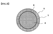
- Fig. 1 is a schematically cross sectional view of a Cu core ball according to an embodiment of the present invention for showing a configuration thereof.
- the Cu core ball 1 of the present embodiment includes a Cu ball 2, and a solder layer 3 covering the Cu ball.
- the solder layer 3 is made of an Ag-free solder alloy composed of not less than 0.1 % through not more than 3.0% of Cu, the remainder being Sn, and the solder layer 3 is formed by subjecting the surface of the Cu ball 2 to solder plating.
- the Cu ball 2 is made of Cu or a Cu alloy containing 50% or more of Cu.
- a diffusion prevention layer 4 is formed between the Cu ball 2 and the solder layer 3.
- the diffusion prevention layer 4 is made of at least one element selected from Ni, Co, or others, and prevents Cu constituting the Cu ball 2 from diffusing into the solder layer 3.
- the Cu core ball 1 in which the solder layer 3, which is made of a solder alloy having an Ag-free composition and has an additive amount of Cu not less than 0.1 % through not more than 3.0%, the remainder being Sn, is formed on a surface of the Cu ball 2 achieves desired levels in both of strength against impacts such as dropping, and strength against stretching by temperature change referred to as heat cycle, even if the object to be jointed is a Cu-OSP substrate composed of a Cu layer whose surface has been subjected to pre-flux treatment, or an electrolytically Ni/Au plated substrate composed of a Cu layer whose surface has subjected to electrolytic Ni/Au plating.
- the solder ball made of an Ag-free solder alloy shows lower strength against heat cycle in comparison with a solder ball made of an Ag-containing solder alloy.
- the solder layer 3 is made of an Ag-free solder alloy, but achieves desired dropping strength and higher strength against heat cycle in comparison with a Cu core ball made of an Ag-containing solder alloy.
- the semiconductor package can be supported by the Cu ball which is not melted at the melting point of the solder alloy even if the weight of the semiconductor packages is applied to the solder bump. Accordingly, the solder bumps is not collapsed by the self-weight of the semiconductor packages.
- solder alloys having a composition that can achieve a low ⁇ dose are under development.
- the Cu ball 2 is covered by the solder layer 3, so that the ⁇ -ray emitted from the Cu ball 2 is likely blocked if the solder alloy constituting the solder layer 3 achieves a low ⁇ dose.
- a composition which achieves such a low ⁇ dose is also required.
- the Cu core ball 1 has low sphericity, flowability during mounting and uniformity of the solder amount decrease when the solder bumps are formed.
- the sphericity is the degree of closeness to a sphere. Therefore, the Cu core ball 1 having high sphericity is desired.
- the composition of the solder layer 3 is a lead-free solder alloy composed mainly of Sn, and is an Sn-Cu alloy from the viewpoint of strength against impacts such as dropping, and strength against heat cycle.
- the thickness of the solder layer 3 is not particularly limited, preferably 100 ⁇ m (one side) or less, and commonly from 1 to 50 ⁇ m.
- the solder layer 3 is formed by circulating the Cu ball 2 and plating solution. Circulation of the plating solution causes the salt formation and precipitation of the elements Pb, Bi, and Po in the plating solution. Once the deposits as salts are formed, they stably exist in the plating solution. Accordingly, the Cu core ball 1 according to the present invention reduces the radioactive element content in the solder layer 3 without inclusion of the deposits in the solder layer 3, and thus can reduce the ⁇ dose in the Cu core ball 1 itself.
- U and Th are radioactive elements so that it is required to limit their contents in order to suppress any software errors.
- the U and Th contents are respectively required to be 5 ppb or less so that the ⁇ dose of the solder plating film is 0.0200 cph/cm 2 or less. Further, preferably, the U and Th contents are respectively 2 ppb or less from a viewpoint of suppressing the software errors in the present or future high density mounting structure.
- the ⁇ dose of the Cu core ball according to this invention is 0.0200 cph/cm 2 or less. This is the ⁇ dose such that it does not cause any software errors in the high density mounting structure of the electronic components.
- the ⁇ dose of the Cu core ball 1 according to this invention is attained by limiting the ⁇ dose of the solder plating film 3 constituting the Cu core ball 1 to be 0.0200 cph/cm 2 or less.
- the ⁇ dose in the Cu core ball 1 is also achieved by, as will be described later, when the ⁇ dose in the Cu ball 2 is 0.0200 cph/cm 2 or less.
- the Cu core ball 1 according to the invention is formed at least at 100 degrees C so that it is difficult to consider that the contents of radioactive isotopes such as U, Th, 210 Po, Bi, Pb and the like is decreased by vaporization of the radioactive isotopes.
- radioactive isotopes such as U, Th, 210 Po, Bi, Pb and the like
- U, Th, Pb, Bi, and 210 Po form salts thereof which are deposited in the plating solution.
- the deposited salts are electrically neutral and they are not brought into the solder plating film even when the plating solution is flown.
- the Cu core ball 1 according to the invention represents low ⁇ dose because such a solder plating film 3 covers it.
- the ⁇ dose is 0.0020 cph/cm 2 or less. It is much preferable that the ⁇ dose is 0.0010 cph/cm 2 or less.
- the lower limit of the impurity amount is not particularly limited, because the content of radioactive elements and the ⁇ dose decrease as the purity of the solder layer 3 constituting the Cu core ball 1 according to the present invention increases, or the impurity content in the solder layer 3 decreases.
- the upper limit is preferably 1000 ppm or less, more preferably 100 ppm or less, even more preferably 50 ppm or less, and particularly preferably 10 ppm or less, from the viewpoint of reducing the ⁇ dose.
- the total impurity amount in the solder layer 3 is the total content of impurities other than Sn and Cu in the solder layer 3.
- the Bi and Pb contents are lower in the impurities contained in the solder layer 3.
- Bi and Pb contain very small amounts of 210 Bi and 210 Pb as radioisotopes, respectively. Accordingly, the reduction of the Bi and Pb contents is considered to markedly reduce the ⁇ dose in the solder layer 3.
- Each of the Bi and Pb contents in the solder layer 3 is preferably 15 ppm or less, more preferably 10 ppm or less, and particularly preferably 0 ppm.
- composition, ⁇ dose, and sphericity of the Cu ball 2 constituting the Cu core ball 1 according to the present invention will describe the composition, ⁇ dose, and sphericity of the Cu ball 2 constituting the Cu core ball 1 according to the present invention more in detail.
- the Cu ball 2 constituting the Cu core ball 1 is not melted at the soldering temperature, so that it can reduce the variation in the solder joint height. Accordingly, it is preferable that the Cu ball 2 has high sphericity and small variation in the diameter thereof. In addition, as described above, it is preferable that the ⁇ dose in the Cu ball 2 is low as in the solder layer 3. The preferred embodiment of the Cu ball 2 will be described below.
- the U and Th are radioisotopes, and their contents may be required to be reduced to prevent software errors.
- Each of the U and Th contents may be required to be 5 ppb or less so as to make the ⁇ dose in the Cu ball 2 0.0200 cph/cm 2 or less.
- each of the U and Th contents is preferably 2 ppb or less.
- the purity of the Cu ball 2 is 3N or more and 4N5 or less.
- the impurity element content in the Cu ball 2 is of 50 ppm or more.
- the purity of metal materials such as Cu is referred to as 2N for 99%, 3N for 99.9%, 4N for 99.99%, and 5N for 99.999%.
- 4N5 means that the purity of the metal material is of 99.995%.
- the Cu material formed in the form of small pieces having a certain shape is melted by heating, and the molten Cu is formed into sphere by the surface tension and coagulated to make the Cu ball 2.
- the crystal grains grow in the spherical molten Cu.
- impurity elements are abundant, these impurity elements work as crystal core, and hinder the growth of crystal grains. Accordingly, the spherical molten Cu forms the Cu ball 2 having a high sphericity owing to the inhibition of the growth of fine crystal grains.
- the amount of impurity elements is small, the amount of crystal core is relatively small, so that the grains grow into a certain direction without inhibition. As a result of this, spherical molten Cu is coagulated with the surface partly protruded. Such a Cu ball has a low sphericity.
- the impurity elements Sn, Sb, Bi, Zn, Fe, Al, As, Ag, In, Cd, Cu, Pb, Au, P, S, U, Th and the like are conceivable.
- the lower limit of the purity is not particularly limited, but is preferably 3N or more, from the viewpoint of suppressing the ⁇ dose and preventing deterioration of electric conduction and heat conductivity of the Cu ball 2 caused by decrease of the purity.
- the content of the impurity elements excluding Cu in the Cu ball 2 is preferably less than 1000 ppm.
- the ⁇ dose in the Cu ball 2 is 0.0200 cph/cm 2 or less. This is ⁇ dose which will not cause problems of software errors in high-density packaging of electronic components.
- heating treatment is carried out again, in addition to the ordinary processes carried out for producing the Cu ball 2. Therefore, 210 Po slightly remaining in the Cu material evaporates, and the Cu ball 2 exhibits a further lower ⁇ dose than that of the Cu material.
- the ⁇ dose is preferably 0.0020 cph/cm 2 or less, and more preferably 0.0010 cph/cm 2 or less, from the viewpoint of preventing software errors in higher density packaging.
- the Cu ball 2 constituting the Cu core ball 1 according to the present invention particularly contains, among these impurity elements, a content of either Pb or Bi, or a total content of Pb and Bi which is 1 ppm or more as the impurity elements.
- a content of either Pb or Bi, or a total content of Pb and Bi which is 1 ppm or more as the impurity elements.
- 210 Pb turns to 210 Bi by ⁇ -decay
- 210 Bi turns to 210 Po by ⁇ -decay
- 210 Po turns to 206 Pb by ⁇ -decay. Therefore, in order to reduce the ⁇ dose, it seems that the content of either Pb or Bi or the content of Pb and Bi as impurity elements is preferably as low as possible.
- the content ratios of 210 Pb contained in Pb and of 210 Bi contained in Bi are low. Accordingly, it seems that if the Pb and Bi contents are reduced to a certain degree, 210 Pb and 210 Bi are sufficiently removed to the degree which allows the reduction of the ⁇ dose to the above-described range.
- the impurity element content is preferably high. When both of Pb and Bi as impurity elements are contained in the Cu material, they work as crystal core during melting in the production process of the Cu ball 2 to increase the sphericity of the Cu ball 2.
- either Pb or Bi or Pb and Bi are contained in an amount which allows the removal of 210 Pb and 210 Bi to the degree where the ⁇ dose is reduced to the above-described range. From this viewpoint, it is preferable that a content of either Pb or Bi, or a total content of Pb and Bi is 1 ppm or more.
- the content of either Pb or Bi, or the total content of Pb and Bi is 10 ppm or more.
- the upper limit thereof is not limited as long as the ⁇ dose is reduced, but it is more preferable that the content of either Pb or Bi, or the total content of Pb and Bi is less than 1000 ppm, from the viewpoint of suppressing deterioration of electric conductivity of the Cu ball 2.
- the Pb content is from 10 ppm to 50 ppm and the Bi content is from 10 ppm to 50 ppm.
- the sphericity of the Cu ball 2 is 0.95 or more, from the viewpoint of controlling the stand-off height. If the sphericity of the Cu ball 2 is less than 0.95, the Cu ball has an indefinite shape, so that bumps having nonuniform heights are formed during bump formation, thereby increasing the possibility of occurrence of jointing defect. It is more preferable that the sphericity is 0.990 or more. In the present invention, sphericity represents the deviation from a true sphere. The sphericity is determined by various kinds of methods such as the least squares center method (LSC method), minimum zone center method (MZC method), the maximum inscribed center method (MIC method), or minimum circumscribed center method (MCC method).
- LSC method least squares center method
- MZC method minimum zone center method
- MIC method maximum inscribed center method
- MCC method minimum circumscribed center method
- sphericity is an arithmetic mean value calculated by dividing the diameter of each of the 500 Cu balls 2 by the major axis. The closer the value to the upper limit 1.00, the closer the true sphere.
- the length of the major axis and diameter are referred to as lengths measured by Ultra Quick Vision, ULTRA QV350-PRO, manufactured by Mitsutoyo Corporation.
- the diameter of the Cu ball 2 is from 1 to 1000 ⁇ m. When the diameter is within this range, the spherical Cu ball 2 is stably produced, and the short circuit caused by a narrow pitch between the terminals can be suppressed.
- the Cu core ball 1 When describing a case to which the Cu core ball 1 according to the present invention is applied, the Cu core ball 1 is used in a solder paste made by mixing and kneading solder powder, the Cu core ball 1, and flux.
- the "Cu core ball” may be referred to as "Cu core powder”.
- Cu core powder is an aggregate of many Cu core balls 1, each of the Cu core balls 1 having the above-described properties.
- the powder is contained in a solder paste, and is discriminated from a single Cu core ball in the use condition.
- the powder is usually used as an aggregate also when the powder is used for the formation of solder bumps, so that the "Cu core powder” used in such form is discriminated from a single Cu core ball.
- the diameter of the Cu core ball is generally from 1 to 300 ⁇ m.
- the Cu core ball 1 according to the present invention is used for a formed solder in which the Cu core balls 1 are dispersed in solder.
- solder paste and the formed solder for example, a solder alloy having a composition of Sn-3Ag-0.5Cu (each value is % by mass) is used.
- the present invention is not limited to this solder alloy.
- the Cu core ball 1 according to the present invention is used for solder joints of electronic components.
- the present invention may be applied to the form of columns, pillars, and pellets including Cu as the core.
- the Cu material as material is put on a plate having heat-resisting property such as ceramics and is heated in a furnace together with the heat-resisting plate.
- a plate having heat-resisting property such as ceramics and is heated in a furnace together with the heat-resisting plate.
- dimples each having a hemispheric bottom in the heat-resisting plate.
- a diameter of the dimple and a depth thereof are suitably set according to a diameter of the Cu ball.
- the diameter thereof is 0.8 mm and the depth thereof is 0.88 mm.
- the Cu materials each having a chip shape hereinafter, referred to as "chip material"
- the heat-resisting plate in which the chip material have been put into each of the dimples is heated up to 1100 through 1300 degrees C in the furnace into which ammonia decomposition gas is filled and heating treatment is performed thereon during 30 through 60 minutes.
- temperature in the furnace is more than the melting point of Cu
- the chip material is fused so that it becomes spherical.
- the interior of the furnace is cooled so that the Cu ball 2 is formed in each of the dimples of the heat-resisting plate.
- the formed Cu ball 2 is again heated at the temperature of 800 through 1000 degrees C which is a temperature that is less than the melting point of Cu.
- the fused Cu is dropped down from an orifice pierced through a bottom of a melting pot and the droplet is cooled to be granulated as the Cu ball 2 and a granulation method in which thermal plasma heats cut metal of Cu at a temperature of 1000 degrees C or more.
- the Cu balls 2 thus granulated may be again heated respectively at a temperature of 800 through 1000 degrees C during 30 through 60 minutes.
- the Cu material which is a raw material of the Cu ball 2 may be heated at a temperature of 800 through 1000 degrees C before the Cu ball 2 is granulated.
- the Cu material which is a raw material of the Cu ball 2
- pellet, wire, pillar or the like can be used as the Cu material which is a raw material of the Cu ball 2.
- the Cu material may have a purity of 99.9% through 99.99% from a viewpoint such that the purity of the Cu ball does not too decrease.
- a temperature for maintaining the fused Cu may decrease to a temperature of about 1000 degrees C, which is similar to a conventional one, without performing the above-mentioned heating treatment.
- the above-mentioned heating treatment may be suitably omitted or changed according to the purity of the Cu material and/or the ⁇ dose thereof.
- the method of forming the plating film 3 on the Cu ball 2 by flowing the plating solution with the Cu balls 2 manufactured as described above there are a electrolytic plating method such as a known barrel plating, a method of generating a high speed turbulent flow in the plating solution within a plating tank by a pump connected to the plating tank and forming the plating film on the Cu ball 2 by the turbulent flow in the plating solution, a method of providing a vibration plate in a plating tank to vibrate it at predetermined frequency so that the plating solution is agitated by high speed turbulent flow and forming the plating film on the Cu ball 2 by the turbulent flow in the plating solution and the like.
- a electrolytic plating method such as a known barrel plating
- a method of generating a high speed turbulent flow in the plating solution within a plating tank by a pump connected to the plating tank and forming the plating film on the Cu ball 2 by the turbulent flow in the plating solution a method of providing a vibration plate in a plating tank
- the Sn-Cu-containing plating solution according to one embodiment of the present invention includes a medium composed mainly of water, and sulfonic acids and Sn and Cu in the form of metal components as essential components.
- the metal components exist in the form of Sn ion (Sn 2+ and/or Sn 4+ ) and Cu ion (Cu + /Cu 2+ ) in the plating solution.
- the plating solution is obtained by mixing a mother plating liquor, which is composed mainly of water and sulfonic acids, and metal compounds, and preferably contains an organic complex agent for stabilizing the metal ions.
- first Sn compounds such as tan salts, tin sulfate, tin oxide, tin nitrate, tin chloride, tin bromide, tin iodide, tin phosphate, tin pyrophosphate, tin acetate, tin formate, tin citrate, tin gluconate, tin tartrate, tin lactate, tin succinate, tin sulfamate, tin borofluoride, tin silicofluoride and the like of organic sulfonic acid such as methanesulfonic acid, ethanesulfonic acid, 2-propanol sulfonic acid, p-phenol sulfonic acid and the like are exemplified.
- organic sulfonic acid such as methanesulfonic acid, ethanesulfonic acid, 2-propanol sulfonic acid, p-
- Cu compounds copper salts, copper sulfate, copper oxide, copper nitrate, copper chloride, copper bromide, copper iodide, copper phosphate, copper pyrophosphate, copper acetate, copper formate, copper citrate, copper gluconate, copper tartrate, copper lactate, copper succinate, copper sulfamate, copper borofluoride, copper silicofluoride and the like of the above-mentioned organic sulfonic acid are exemplified.
- a single species of these Cu compounds can be used or two species or more thereof can be mixed and used.
- Blending quantities of respective metals in the plating solution are as follows: As Sn 2+ , 0.05 through 2 mol/L, preferably 0.25 through 1 mol/L; and As Cu, 0.002 through 0.02 mol/L, preferably 0.003 through 0.01 mol/L.
- Sn 2+ that relates to the plating
- a quantity of Sn 2+ may be adjusted in this invention.
- a desired deposition amount of a solder plating is estimated according to a following formula (1) based on the Faraday's law of electrolysis and an amount of electricity therefor is calculated.
- the electric current flows through the plating solution so as to be the calculated amount of electricity and the plating is executed while the plating solution flows with the Cu balls.
- a volume of the plating tank may be fixed according to a total input amount of the Cu balls and the plating solution.
- w is an electrolytic deposition amount (g); 1 is electric current (A); t is electricity energizing time (second); M is an atomic weight of a deposited element (in a case of Sn, 118.71); Z is an atomic value (in a case of Sn, bivalent); and F is the Faraday constant (96500 coulombs).
- Q A ⁇ Sec
- the plating has been executed in this invention while the plating solution flows with the Cu balls, a flowing method thereof is not particularly limited.
- the plating solution may flow with the Cu balls by a rotation of barrel like the barrel electrolytic plating method.
- any drying is executed in the air or under N2 atmosphere, so that it is possible to obtain the Cu core ball according to the invention.
- a Cu core ball in which a solder layer was made of an Ag-free solder alloy, a Cu core ball in which a solder layer was made of an Ag-containing solder alloy, a solder ball made of an Ag-free solder alloy, and a solder ball made of an Ag-containing solder alloy were prepared, and the dropping strength test for measuring the strength against impacts such as dropping, and the heat cycle test for measuring the strength against stretching by heat cycle were carried out.
- the Cu core ball 1 shown in Fig. 1 in Executed Example 1, the Cu core ball 1 having a diameter of 300 ⁇ m was prepared.
- the Cu core ball 1 of Executed Example 1 was composed of the Cu ball 2 having a diameter of 250 ⁇ m, the diffusion prevention layer 4 made of Ni having a film thickness of 2 ⁇ m on one side, and the solder layer 3 made of an Sn-Cu alloy.
- the composition of the Sn-Cu alloy was Sn-0.7Cu, and tan additive amount of Cu in the solder layer 3 was 0.7%.
- Comparative Example 1 As a comparative example, in Comparative Example 1, a Cu core ball having a solder layer made of an Sn-Ag-Cu alloy was prepared. The composition of the Sn-Ag-Cu alloy was Sn-1.0Ag-0.7Cu. In Comparative Example 2, a solder ball was prepared from an Sn-Cu alloy having the same composition as Executed Example 1. In Comparative Example 3, a solder ball was prepared from an Sn-Ag-Cu alloy having the same composition as Comparative Example 1.
- a resist film having a film thickness of 15 ⁇ m was formed on the semiconductor package substrates used in the heat cycle test and the dropping strength test, an opening having a diameter of 240 ⁇ m was formed in the resist film, and the Cu core balls or solder balls of Executed Example or Comparative Example were jointed in a reflow furnace.
- the reflowing conditions were as follows; both of the heat cycle test and dropping strength test were carried out in a N 2 atmosphere with the peak temperature of 245°C, the preliminary heating was carried out at 140 to 160°C for 20 seconds, and the main heating was carried out at 220°C or higher for 40 seconds.
- the semiconductor package substrates to which the Cu core balls or the solder balls had been jointed, were mounted on the printed circuit boards for the heat cycle test and the dropping strength test, respectively.
- a solder paste having a solder alloy composition of Sn-3.0Ag-0.5Cu was printed at a thickness of 100 ⁇ m and a diameter of 240 ⁇ m for both the heat cycle test and the dropping strength test.
- the semiconductor package substrates, to which the Cu core balls or the solder balls had been jointed, of Executed Example or Comparative Example were connected to a printed circuit board in a reflow furnace.
- the reflowing conditions were as follows; this was carried out in the atmosphere with a peak temperature of 245°C, the preliminary heating was carried out at 140 to 160°C for 70 seconds, and the main heating was carried out at 220°C or higher for 40 seconds.
- the evaluation substrate thus made was fixed at the both ends using a special jig with it being floated from the base at the position 10 mm.
- impacts of an acceleration of 1500 G were repeatedly applied, and the point at which the resistance value increased by 1.5 times in comparison with the initial resistance value was regarded as rupture, and the number of dropping was recorded.
- the resistance of the evaluation substrate thus made was continuously measured by a series circuit.
- a thermal shock apparatus TSA101LA manufactured by ESPEC Corp. treatments at -40°C and +125°C each for 10 minutes were set to be one cycle, the point at which the resistance value exceeded 15 ⁇ was regarded as rupture, and the time of heat fatigue cycle when all the solder joints on the 15 semiconductor package substrates on the printed circuit board were destroyed was recorded.
- 10 sets of evaluation substrates were prepared, ten times of test were carried out, and the average value was used as the result.
- Table 1 shows the test result when the semiconductor package substrate was a Cu-OSP substrate composed of a Cu layer whose surface had been subjected to pre-flux treatment. [Table 1] Executed Example 1 Comparative Example 1 Comparative Example 2 Comparative Example 3 Dropping strength >100 >100 >100 >100 Strength against heat cycle 1734 1575 1328 2064
- the semiconductor package substrate was the Cu-OSP substrate having the Cu layer whose surface had been subjected to pre-flux treatment, as shown in Table 1, in the Cu core ball of Executed Example 1 having a solder layer made of an Sn-Cu alloy, the dropping strength was improved, and the strength against heat cycle was higher than the required 1500 times.
- the semiconductor package substrate was the Cu-OSP substrate
- the Cu core ball of Comparative Example 1 having a solder layer made of an Sn-Ag-Cu alloy, the desired dropping strength was achieved, but the strength against heat cycle was deteriorated.
- the semiconductor package substrate was the Cu-OSP substrate
- the solder ball of Comparative Example 2 made of an Sn-Cu alloy the dropping strength was improved, but the strength against heat cycle was deteriorated.
- the solder ball of Comparative Example 3 made of an Sn-Ag-Cu alloy required values of the dropping strength and the strength against heat cycle were achieved.
- the Cu core ball of Executed Example 1 achieved sufficient dropping strength and strength against heat cycle.
- the additive amount of Cu in the solder layer being from 0.1 % to 3.0%
- both of the dropping strength and strength against heat cycle achieved the values higher than the required levels.
- the additive amount of Cu is about 3.0%
- the solder alloy has a high melting point. Therefore, it is preferable that the additive amount of Cu in the solder layer made of an Sn-Cu alloy is not less than 0.1 % through not more than 2.0%.
- the manufacture condition of the Cu ball having the high sphericity was searched.
- Cu pellets each having a purity of 99.9%, Cu wires each having a purity of 99.995% or less and Cu plates each having a purity exceeding 99.995% were prepared. They were respectively put into the melting pot, the temperature of the melting pot was then risen to 1200 degrees C and this heating treatment was performed during 45 minutes. The fused Cu was dropped down from an orifice pierced through the bottom of the melting pot and the droplet was cooled so as to be granulated as the Cu ball. Thus, the Cu balls having a mean diameter of 250 ⁇ m were manufactured.
- a table 3 shows a result of an elementary analysis and sphericity of the manufactured Cu balls.
- the following will describe a method for measuring the sphericity more in detail.
- the sphericity was measured by CNC image measurement system.
- Equipment therefor was ultra quick vision, ULTRA QV350-PRO manufactured by MITSUTOYO Corporation.
- the method for measuring the ⁇ dose is as follows.
- the ⁇ dose was measured using ⁇ dose measurement equipment of a gas-flow proportional counter.
- a measurement sample was a 300 x 300 mm flat shallow container with the Cu balls spreading all over it. This measurement sample was put into the ⁇ dose measurement equipment and the ⁇ dose was measured after it stood for 24 hours under PR-10 gas flow.
- the PR-10 gas (90% of argon and 10% of methane) used in the measurement was the gas after more than three weeks was elapsed since the gas was filled in a gas bomb. It complied with a guideline of the method of measuring the ⁇ dose, which was prescribed by joint electron device engineering council (JEDEC), that the bomb was used after more than three weeks was elapsed, so that ⁇ ray did not occur by radon in the atmosphere, which might be inserted into the gas bomb.
- JEDEC joint electron device engineering council
- the unit of the elemental analysis result of the alloy composition is mass ppb only for U and Th.
- the units of the other elements and total impurity amount are mass ppm.
- the Cu balls made of Cu wire having purity of 99.995% or less were covered by an Sn solder plating film under the following conditions, thereby making Cu core balls of Executed Example 2.
- the Cu core balls of Executed Example 2 were subjected to plating treatment using the following plating solution, in such a manner that the Cu balls having a diameter of 250 ⁇ m were coated with a solder layer having a film thickness (one side) of 50 ⁇ m, at a quantity of electricity of about 0.17 coulomb.
- the cross section of the Cu core ball coated with a solder plating film was observed by a SEM photograph.
- the film thickness was about 50 ⁇ m. After the treatment, the balls were dried in the air, thereby obtaining Cu core balls.
- the solder plating solution was prepared as follows. a 54% by weight of methane sulfonic acid aqueous solution was all put into one third of water, which was required to a preparation of the plating solution, within a stirring container and they were put into the stirring container in advance. Subsequently, acetyl cysteine, which was an example of mercaptan compound that was a complexing agent, was put thereinto and after its dissolution was confirmed, 2, 2'-dithiodianiline, which was an example of aromatic amino compound that was another complexing agent, was put thereinto. When the liquid turned out to be a light blue gelled liquid, stannous trifluoromethanesulfonate was immediately put thereinto.
- the stannous trifluoromethanesulfonate used in the present Executed Examples was prepared from the following Sn sheet material.
- the elemental analysis of the Sn sheet material which was raw material of the solder plating solution, and the elemental analysis of the solder plating film formed on a surface of the Cu core ball were carried out by high frequency inductively coupled plasma mass spectrometry (ICP-MS analysis) for U and Th, and high frequency inductively coupled plasma atomic emission spectral analysis (ICP-AES analysis) for other elements.
- ICP-MS analysis high frequency inductively coupled plasma mass spectrometry
- ICP-AES analysis high frequency inductively coupled plasma atomic emission spectral analysis
- the ⁇ dose of the Sn sheet material was measured in the same manner as for the Cu ball, except that the Sn sheet material was spread on a flat shallow container of 300 mm x 300 mm.
- the ⁇ dose of the Cu core ball was measured in the same manner as for the above-described Cu ball.
- the sphericity of the Cu core ball was also measured under the same conditions for the Cu ball. Table 3 shows the results of these measurements.
- the ⁇ dose of the Sn sheet material was measured.
- the unit of the elemental analysis result of the alloy composition is mass ppb only for U and Th.
- the units of the other elements and total impurity amount are mass ppm.
- Table 3 indicates that the ⁇ dose was higher than 0.2000 cph/cm 2 in the stage of the Sn sheet material, but the ⁇ dose was less than 0.0010 cph/cm 2 in Executed Example 2 wherein a solder layer of an Sn-Cu alloy was formed on the Cu ball using the Sn sheet material. It was verified that the ⁇ dose of the Cu core ball of Executed Example 2 was reduced by forming a solder plating film by a plating method.
- the Cu core balls of Executed Example 2 showed no increase in the ⁇ dose, even after the lapse of two years after making.
- the shape of the present invention is not limited to a ball as long as the purpose of preventing the collapse of solder bumps by the self weight of the semiconductor packages can be achieved, and it may be applied to the above-described Cu core column. Specifically, it may be applied to a column or a shaft of a column such as a triangle or square column which is composed of upper and lower surfaces having three or more sides directly contacting with the substrate.
- the Cu column to be the core may be formed by a known method, and the plating film covering the surface of the Cu column may be also formed by the above-described method used for the Cu core ball.
- Fig. 2 is a schematically cross sectional side view of the Cu core column of the present embodiment for showing the configuration thereof and Fig. 3 is a schematically sectional plane view of the Cu core column of the present embodiment for showing the configuration thereof.
- the Cu core column 5 of the present embodiment is composed of a Cu column 6, and a solder layer 7 covering the Cu column 6.
- the diameter of each of the top and bottom surfaces of the Cu column 6 constituting the Cu core column 5 according to the present invention is preferably from 1 to 1000 ⁇ m.
- the diameter is more preferably from 1 to 300 ⁇ m, even more preferably from 1 to 200 ⁇ m, and most preferably from 1 to 100 ⁇ m.
- the height L of the Cu column 6 is preferably from 1 to 3000 ⁇ m.
- the height is more preferably from 1 to 300 ⁇ m, even more preferably from 1 to 200 ⁇ m, and most preferably from 1 to 100 ⁇ m.
- Preferred conditions of the purity, ⁇ dose, impurity content and the like of the Cu column 6 constituting the Cu core column 5 according to the present invention other than the size of the Cu column 6 are the same as those for the Cu ball 2 according to the present invention.
- the sphericity is not required, so that there is no need to make the purity 4N5 or less, or make the impurity element content 50 ppm or more.
- the dropping strength and strength against heat cycle is not influenced even if the impurity content is not minimized.
- solder composition preferred conditions of the solder composition, ⁇ dose, and impurity content of the solder layer 7 constituting the Cu core column 5 according to the present invention are the same as those for the solder layer 3 according to the present invention.
- preferred conditions of the ⁇ dose and the like of the Cu core column 5 according to the present invention are the same as those for the Cu core ball 1 according to the present invention.
- the Cu core column 5 according to the present invention may have a diffusion prevention layer 8 formed between the Cu column 6 and the solder layer 7.
- the diffusion prevention layer 8 is composed of one or more elements selected from Ni, Co, and others, and prevents Cu composing the Cu column 6 from diffusing into the solder layer 7.
- the Cu core column 5 may be used in a through-silicon via (TSV) for connecting the electrodes between the laminated semiconductor chips.
- TSV is produced by boring a hole in silicon by etching, forming an insulating layer and then a through-silicon conductor thereon in the hole in this order, polishing the upper and lower surfaces of the silicon, and exposing the through-silicon conductor at the upper and lower surfaces.
- the through-silicon conductor has been ordinarily formed by filling the hole with Cu or the like by plating.
- the entire surface of the silicon is immersed in a plating solution, so that adsorption of impurities or moisture can occur.
- the Cu core column 5 according to the present invention may be directly inserted into the hole formed in the silicon on a height direction, and used as a through-silicon conductor.
- the Cu core column 5 When the Cu core column 5 is inserted into the silicon, it may be jointed by a solder material such as a solder paste.
- the Cu core column 5 when the Cu core column 5 is inserted into the silicon, it may be jointed by a flux alone. As a result of this, failures such as the adsorption of impurities or moisture can be prevented, and the omission of the plating process can reduce the cost and time of manufacturing.
- the above-described Cu core column 5 according to the present invention can achieve dropping strength and strength against heat cycle equivalent or superior to those of the solder column.
Abstract
Description
- The present invention relates to a Cu core ball in which a Cu ball is covered by a solder alloy, a solder paste using the Cu core ball, a formed solder using the Cu core ball, and a solder joint using the Cu core ball and also relates to a Cu core column and a solder joint using the Cu core column.
- In recent years, with the development of small-size information equipment, rapid miniaturization has been advanced in electronic components mounted thereon. In order to cope with narrowing of connection terminals and reduction of mounting areas according to downsizing requirement, a ball grid array (hereinafter, referred to as "BGA") in which electrodes are arranged on the rear surface thereof is applied to the electronic component.
- The electronic component to which BGA is applied is, for example, a semiconductor package. In the semiconductor package, a semiconductor chip having electrodes are sealed with any resin. Solder bumps are formed on the electrodes of semiconductor chip. Each solder bump is formed by connecting a solder ball which is formed by making the solder a ball or a solder column which is formed by making the solder a column to the electrode of the semiconductor chip. The semiconductor package to which BGA is applied is mounted on a printed circuit board in such a manner that each solder bump is in contact with a conductive land on the printed circuit board, and by connecting the solder bumps molded by heating to the land, the semiconductor package is mounted on the printed circuit board. In addition, in order to cope with the demand for higher density packaging, a three dimensional high density mounting structure, in which the semiconductor packages are piled along a height direction thereof, has been studied.
- However, when BGA is applied to semiconductor packages to which the three dimensional high density mounting structure is applied, solder balls are collapsed by the self-weight of the semiconductor packages, so that short circuits occur between the electrodes. This may hinder the high-density packaging.
- Therefore, solder bumps using, for example, a Cu core ball or a Cu core column, in which a ball having a micro-diameter or a column made of metal such as Cu having a higher melting point than that of a solder is formed as a core, and the surface of the ball or column is covered by the solder, have been studied. In the solder bumps each having the Cu ball or the like, the semiconductor package can be supported by the Cu ball which is not molded at the melting point of the solder even if the weight of the semiconductor packages is applied to the solder bumps during packaging of the electronic components on the printed circuit board. Accordingly, the solder bumps are not collapsed by the self-weight of the semiconductor packages.
Patent Document 1 is illustrated as an example of the technologies related to the Cu core ball. - Patent Document 1: Japanese Patent Application Publication No.
2010-99736 - By the way, solder bumps made using the solder ball, the solder column, the Cu core ball, or the Cu core column are required to have strength against impacts such as dropping, and strength against stretching by temperature change referred to as "heat cycle".
- A solder ball made of a solder alloy containing Ag achieves desired levels in both of dropping strength and strength against heat cycle. Even with a solder alloy referred to as low-Ag in which the additive amount of Ag is reduced to about 1.0% for cost saving of the solder alloy, the desired levels in both of dropping strength and strength against heat cycle are achieved.
- On the other hand, a solder ball made of a solder alloy free from Ag achieves a desired level of dropping strength, but deteriorates in the strength against heat cycle.
- The problems of the present invention are to achieve desired dropping strength and strength against heat cycle in a Cu core ball at the same level as or more than those of a solder ball or a solder column, and to provide such a Cu core ball, a solder paste, a formed solder, and a solder joint, which use the Cu core ball, a Cu core column, and a solder joint using the Cu core column.
- The inventors have found that a Cu core ball in which a Cu ball is covered by an Ag-free solder alloy, and a Cu core column in which a Cu column is covered by an Ag-free solder alloy, have an equal dropping strength and a higher strength against heat cycle in comparison with the solder ball or solder column made of an Ag-free solder alloy.
- The present invention is as follows.
- (1) A Cu core ball including a core layer made of Cu or a Cu alloy containing 50% or more of Cu, and a solder layer made of a solder alloy composed of Sn and Cu, the solder layer covering the core layer.
- (2) The Cu core ball of the above item (1), wherein the solder layer contains not less than 0.1 % through not more than 3.0% of Cu, the remainder being composed of Sn and impurities.
- (3) The Cu core ball of the above item (2), wherein the core layer covered by a layer made of at least one element selected from Ni and Co is covered by the solder layer.
- (4) The Cu core ball of the above item (3), wherein an α dose is 0.0200 cph/cm2 or less.
- (5) A solder paste including the Cu core ball of any one of the above items (1) to (4).
- (6) A formed solder including the Cu core ball of any one of the above items (1) to (4).
- (7) A solder joint including the Cu core ball of any one of the above items (1) to (4).
- (8) A Cu core column including a core layer made of Cu or a Cu alloy containing 50% or more of Cu, and a solder layer made of a solder alloy composed of Sn and Cu, the solder layer covering the core layer.
- (9) The Cu core column of the above item (8), wherein the solder layer contains not less than 0.1% through not more than 3.0% of Cu, the remainder being composed of Sn and impurities.
- (10) The Cu core column of the above item (9), wherein the core layer covered by a layer made of at least one element selected from Ni and Co is covered by the solder layer.
- (11) The Cu core column of the above item (10), wherein an α dose is 0.0200 cph/cm2 or less.
- (12) A solder joint including the Cu core column of any one of the above items (8) to (11).
- The present invention achieves desired levels in both of dropping strength and strength against heat cycle. Although the solder ball prepared from the Ag-free solder alloy has reduced the strength against heat cycle as compared with the solder ball prepared from the Ag-containing solder alloy, in the present invention, required dropping strength and improved strength against heat cycle are achieved as compared with the Cu core ball prepared from the Ag-containing solder alloy. The same applies to a Cu core column, and required dropping strength and improved strength against heat cycle are achieved as compared with the Cu core column prepared from the Ag-containing solder alloy.
-
-
Fig. 1 is a schematically cross sectional view of a Cu core ball according to an embodiment of the present invention for showing a configuration thereof; -
Fig. 2 is a schematically cross sectional side view of a Cu core column according to an embodiment of the present invention for showing a configuration thereof; and -
Fig. 3 is a schematically cross sectional plane view of the Cu core column according to the embodiment of the present invention for showing the configuration thereof. - The following will describe an embodiment below more in detail in which this invention is applied to a Cu core ball. In the present description, the units relating the composition of the Cu core ball (ppm, ppb, and %) represent the proportions with reference to the mass (mass ppm, mass ppb, and % by mass), unless otherwise specified.
-
Fig. 1 is a schematically cross sectional view of a Cu core ball according to an embodiment of the present invention for showing a configuration thereof. TheCu core ball 1 of the present embodiment includes a Cu ball 2, and asolder layer 3 covering the Cu ball. - The
solder layer 3 is made of an Ag-free solder alloy composed of not less than 0.1 % through not more than 3.0% of Cu, the remainder being Sn, and thesolder layer 3 is formed by subjecting the surface of the Cu ball 2 to solder plating. The Cu ball 2 is made of Cu or a Cu alloy containing 50% or more of Cu. - In the
Cu core ball 1, adiffusion prevention layer 4 is formed between the Cu ball 2 and thesolder layer 3. Thediffusion prevention layer 4 is made of at least one element selected from Ni, Co, or others, and prevents Cu constituting the Cu ball 2 from diffusing into thesolder layer 3. - The
Cu core ball 1 in which thesolder layer 3, which is made of a solder alloy having an Ag-free composition and has an additive amount of Cu not less than 0.1 % through not more than 3.0%, the remainder being Sn, is formed on a surface of the Cu ball 2 achieves desired levels in both of strength against impacts such as dropping, and strength against stretching by temperature change referred to as heat cycle, even if the object to be jointed is a Cu-OSP substrate composed of a Cu layer whose surface has been subjected to pre-flux treatment, or an electrolytically Ni/Au plated substrate composed of a Cu layer whose surface has subjected to electrolytic Ni/Au plating. - The solder ball made of an Ag-free solder alloy shows lower strength against heat cycle in comparison with a solder ball made of an Ag-containing solder alloy. In the
Cu core ball 1 of the present embodiment, thesolder layer 3 is made of an Ag-free solder alloy, but achieves desired dropping strength and higher strength against heat cycle in comparison with a Cu core ball made of an Ag-containing solder alloy. - In the solder bump in which the
Cu core ball 1 is used, the semiconductor package can be supported by the Cu ball which is not melted at the melting point of the solder alloy even if the weight of the semiconductor packages is applied to the solder bump. Accordingly, the solder bumps is not collapsed by the self-weight of the semiconductor packages. - By the way, the miniaturization of electronic components allows high-density packaging, but high-density packaging causes software error problems. Software errors are caused by rewriting of the memory which can be caused by the entry of α-ray into the memory cells of a semiconductor integrated circuit (hereinafter referred to as "IC").
- It is considered that the α-ray is emitted by α-decay of radioisotopes such as U, Th, and 210Po as impurities contained in a solder alloy. Therefore, solder alloys having a composition that can achieve a low α dose are under development.
- In the
Cu core ball 1, the Cu ball 2 is covered by thesolder layer 3, so that the α-ray emitted from the Cu ball 2 is likely blocked if the solder alloy constituting thesolder layer 3 achieves a low α dose. In the Cu ball 2, however, a composition which achieves such a low α dose is also required. - Furthermore, if the
Cu core ball 1 has low sphericity, flowability during mounting and uniformity of the solder amount decrease when the solder bumps are formed. The sphericity is the degree of closeness to a sphere. Therefore, theCu core ball 1 having high sphericity is desired. - The composition of the
solder layer 3 is a lead-free solder alloy composed mainly of Sn, and is an Sn-Cu alloy from the viewpoint of strength against impacts such as dropping, and strength against heat cycle. In theCu core ball 1, the thickness of thesolder layer 3 is not particularly limited, preferably 100 µm (one side) or less, and commonly from 1 to 50 µm. - The
solder layer 3 is formed by circulating the Cu ball 2 and plating solution. Circulation of the plating solution causes the salt formation and precipitation of the elements Pb, Bi, and Po in the plating solution. Once the deposits as salts are formed, they stably exist in the plating solution. Accordingly, theCu core ball 1 according to the present invention reduces the radioactive element content in thesolder layer 3 without inclusion of the deposits in thesolder layer 3, and thus can reduce the α dose in theCu core ball 1 itself. - The following will describe the composition of the
solder layer 3 achieving a low α dose below more in detail. - U and Th are radioactive elements so that it is required to limit their contents in order to suppress any software errors. The U and Th contents are respectively required to be 5 ppb or less so that the α dose of the solder plating film is 0.0200 cph/cm2 or less. Further, preferably, the U and Th contents are respectively 2 ppb or less from a viewpoint of suppressing the software errors in the present or future high density mounting structure.
- The α dose of the Cu core ball according to this invention is 0.0200 cph/cm2 or less. This is the α dose such that it does not cause any software errors in the high density mounting structure of the electronic components. The α dose of the
Cu core ball 1 according to this invention is attained by limiting the α dose of thesolder plating film 3 constituting theCu core ball 1 to be 0.0200 cph/cm2 or less. In addition, the α dose in theCu core ball 1 is also achieved by, as will be described later, when the α dose in the Cu ball 2 is 0.0200 cph/cm2 or less. - The
Cu core ball 1 according to the invention is formed at least at 100 degrees C so that it is difficult to consider that the contents of radioactive isotopes such as U, Th, 210Po, Bi, Pb and the like is decreased by vaporization of the radioactive isotopes. However, when plating is performed while the plating solution and the Cu ball 2 are flown, U, Th, Pb, Bi, and 210Po form salts thereof which are deposited in the plating solution. The deposited salts are electrically neutral and they are not brought into the solder plating film even when the plating solution is flown. - Accordingly, their contents in the solder plating film are considerably decreased. Therefore, the
Cu core ball 1 according to the invention represents low α dose because such asolder plating film 3 covers it. From a viewpoint of suppressing any software errors in the higher density mounting structure, it is preferable that the α dose is 0.0020 cph/cm2or less. It is much preferable that the α dose is 0.0010 cph/cm2 or less. - The lower limit of the impurity amount is not particularly limited, because the content of radioactive elements and the α dose decrease as the purity of the
solder layer 3 constituting theCu core ball 1 according to the present invention increases, or the impurity content in thesolder layer 3 decreases. On the other hand, the upper limit is preferably 1000 ppm or less, more preferably 100 ppm or less, even more preferably 50 ppm or less, and particularly preferably 10 ppm or less, from the viewpoint of reducing the α dose. - The total impurity amount in the
solder layer 3 is the total content of impurities other than Sn and Cu in thesolder layer 3. - It is preferable that in particular, the Bi and Pb contents are lower in the impurities contained in the
solder layer 3. Bi and Pb contain very small amounts of 210Bi and 210Pb as radioisotopes, respectively. Accordingly, the reduction of the Bi and Pb contents is considered to markedly reduce the α dose in thesolder layer 3. Each of the Bi and Pb contents in thesolder layer 3 is preferably 15 ppm or less, more preferably 10 ppm or less, and particularly preferably 0 ppm. - Then, the following will describe the composition, α dose, and sphericity of the Cu ball 2 constituting the
Cu core ball 1 according to the present invention more in detail. - When the
Cu core ball 1 according to the present invention is used in solder bumps, the Cu ball 2 constituting theCu core ball 1 is not melted at the soldering temperature, so that it can reduce the variation in the solder joint height. Accordingly, it is preferable that the Cu ball 2 has high sphericity and small variation in the diameter thereof. In addition, as described above, it is preferable that the α dose in the Cu ball 2 is low as in thesolder layer 3. The preferred embodiment of the Cu ball 2 will be described below. - As described above, the U and Th are radioisotopes, and their contents may be required to be reduced to prevent software errors. Each of the U and Th contents may be required to be 5 ppb or less so as to make the α dose in the Cu ball 2 0.0200 cph/cm2 or less. In addition, in order to prevent software errors in the present or future high-density packaging, each of the U and Th contents is preferably 2 ppb or less.
- The purity of the Cu ball 2 is 3N or more and 4N5 or less. In other words, the impurity element content in the Cu ball 2 is of 50 ppm or more. Here, the purity of metal materials such as Cu is referred to as 2N for 99%, 3N for 99.9%, 4N for 99.99%, and 5N for 99.999%. 4N5 means that the purity of the metal material is of 99.995%.
- When the purity of Cu constituting the Cu ball 2 is within this range, a sufficient amount of crystal core for increasing the sphericity of the Cu ball 2 can be secured in the molten Cu. The reason for the increase in the sphericity will be specified as follows.
- When the Cu balls are produced, the Cu material formed in the form of small pieces having a certain shape is melted by heating, and the molten Cu is formed into sphere by the surface tension and coagulated to make the Cu ball 2. During coagulation of the molten Cu from a liquid state, the crystal grains grow in the spherical molten Cu. At this moment, if impurity elements are abundant, these impurity elements work as crystal core, and hinder the growth of crystal grains. Accordingly, the spherical molten Cu forms the Cu ball 2 having a high sphericity owing to the inhibition of the growth of fine crystal grains.
- On the other hand, if the amount of impurity elements is small, the amount of crystal core is relatively small, so that the grains grow into a certain direction without inhibition. As a result of this, spherical molten Cu is coagulated with the surface partly protruded. Such a Cu ball has a low sphericity. As the impurity elements, Sn, Sb, Bi, Zn, Fe, Al, As, Ag, In, Cd, Cu, Pb, Au, P, S, U, Th and the like are conceivable.
- The lower limit of the purity is not particularly limited, but is preferably 3N or more, from the viewpoint of suppressing the α dose and preventing deterioration of electric conduction and heat conductivity of the Cu ball 2 caused by decrease of the purity. In other words, the content of the impurity elements excluding Cu in the Cu ball 2 is preferably less than 1000 ppm.
- The α dose in the Cu ball 2 is 0.0200 cph/cm2 or less. This is α dose which will not cause problems of software errors in high-density packaging of electronic components. In the present invention, heating treatment is carried out again, in addition to the ordinary processes carried out for producing the Cu ball 2. Therefore, 210Po slightly remaining in the Cu material evaporates, and the Cu ball 2 exhibits a further lower α dose than that of the Cu material. The α dose is preferably 0.0020 cph/cm2 or less, and more preferably 0.0010 cph/cm2 or less, from the viewpoint of preventing software errors in higher density packaging.
- As impurity elements contained in the Cu ball 2, Sn, Sb, Bi, Zn, Fe, Al, As, Ag, In, Cd, Cu, Pb, Au, P, S, U, Th and the like are conceivable. It is preferable that the Cu ball 2 constituting the
Cu core ball 1 according to the present invention particularly contains, among these impurity elements, a content of either Pb or Bi, or a total content of Pb and Bi which is 1 ppm or more as the impurity elements. In the present invention, in order to reduce the α dose, it is not required that the content of either Pb or Bi, or the total content of Pb and Bi is reduced to the minimum thereof. The reason is as follows. - 210Pb turns to 210Bi by β-decay, and 210Bi turns to 210Po by β-decay, and 210Po turns to 206Pb by α-decay. Therefore, in order to reduce the α dose, it seems that the content of either Pb or Bi or the content of Pb and Bi as impurity elements is preferably as low as possible.
- However, the content ratios of 210Pb contained in Pb and of 210Bi contained in Bi are low. Accordingly, it seems that if the Pb and Bi contents are reduced to a certain degree, 210Pb and 210 Bi are sufficiently removed to the degree which allows the reduction of the α dose to the above-described range. On the other hand, in order to increase the sphericity of the Cu ball 2, as described above, the impurity element content is preferably high. When both of Pb and Bi as impurity elements are contained in the Cu material, they work as crystal core during melting in the production process of the Cu ball 2 to increase the sphericity of the Cu ball 2. Therefore, it is preferred that either Pb or Bi or Pb and Bi are contained in an amount which allows the removal of 210Pb and 210Bi to the degree where the α dose is reduced to the above-described range. From this viewpoint, it is preferable that a content of either Pb or Bi, or a total content of Pb and Bi is 1 ppm or more.
- It is more preferable that the content of either Pb or Bi, or the total content of Pb and Bi is 10 ppm or more. The upper limit thereof is not limited as long as the α dose is reduced, but it is more preferable that the content of either Pb or Bi, or the total content of Pb and Bi is less than 1000 ppm, from the viewpoint of suppressing deterioration of electric conductivity of the Cu ball 2. It is more preferable that the Pb content is from 10 ppm to 50 ppm and the Bi content is from 10 ppm to 50 ppm.
- It is preferable that the sphericity of the Cu ball 2 is 0.95 or more, from the viewpoint of controlling the stand-off height. If the sphericity of the Cu ball 2 is less than 0.95, the Cu ball has an indefinite shape, so that bumps having nonuniform heights are formed during bump formation, thereby increasing the possibility of occurrence of jointing defect. It is more preferable that the sphericity is 0.990 or more. In the present invention, sphericity represents the deviation from a true sphere. The sphericity is determined by various kinds of methods such as the least squares center method (LSC method), minimum zone center method (MZC method), the maximum inscribed center method (MIC method), or minimum circumscribed center method (MCC method). More specifically, sphericity is an arithmetic mean value calculated by dividing the diameter of each of the 500 Cu balls 2 by the major axis. The closer the value to the upper limit 1.00, the closer the true sphere. In the present invention, the length of the major axis and diameter are referred to as lengths measured by Ultra Quick Vision, ULTRA QV350-PRO, manufactured by Mitsutoyo Corporation.
- It is preferable that the diameter of the Cu ball 2 is from 1 to 1000 µm. When the diameter is within this range, the spherical Cu ball 2 is stably produced, and the short circuit caused by a narrow pitch between the terminals can be suppressed.
- When describing a case to which the
Cu core ball 1 according to the present invention is applied, theCu core ball 1 is used in a solder paste made by mixing and kneading solder powder, theCu core ball 1, and flux. Here, in a case where theCu core ball 1 according to the present invention is used in the solder paste, the "Cu core ball" may be referred to as "Cu core powder". - "Cu core powder" is an aggregate of many
Cu core balls 1, each of theCu core balls 1 having the above-described properties. For example, the powder is contained in a solder paste, and is discriminated from a single Cu core ball in the use condition. In the same manner, the powder is usually used as an aggregate also when the powder is used for the formation of solder bumps, so that the "Cu core powder" used in such form is discriminated from a single Cu core ball. When "Cu core ball" is used in the form referred to as "Cu core powder", the diameter of the Cu core ball is generally from 1 to 300 µm. - In addition, the
Cu core ball 1 according to the present invention is used for a formed solder in which theCu core balls 1 are dispersed in solder. In the solder paste and the formed solder, for example, a solder alloy having a composition of Sn-3Ag-0.5Cu (each value is % by mass) is used. Further, the present invention is not limited to this solder alloy. Furthermore, theCu core ball 1 according to the present invention is used for solder joints of electronic components. In addition, the present invention may be applied to the form of columns, pillars, and pellets including Cu as the core. - The following will describe an example of a method of manufacturing the
Cu core ball 1 according to this invention. - The Cu material as material is put on a plate having heat-resisting property such as ceramics and is heated in a furnace together with the heat-resisting plate. There are many dimples each having a hemispheric bottom in the heat-resisting plate. A diameter of the dimple and a depth thereof are suitably set according to a diameter of the Cu ball. For example, the diameter thereof is 0.8 mm and the depth thereof is 0.88 mm. Further, the Cu materials each having a chip shape (hereinafter, referred to as "chip material"), which are obtained by cutting a fine wire made of Cu, are put into the dimples one by one in the heat-resisting plate.
- The heat-resisting plate in which the chip material have been put into each of the dimples is heated up to 1100 through 1300 degrees C in the furnace into which ammonia decomposition gas is filled and heating treatment is performed thereon during 30 through 60 minutes. In this moment, when temperature in the furnace is more than the melting point of Cu, the chip material is fused so that it becomes spherical. Thereafter, the interior of the furnace is cooled so that the Cu ball 2 is formed in each of the dimples of the heat-resisting plate. After the cooling, the formed Cu ball 2 is again heated at the temperature of 800 through 1000 degrees C which is a temperature that is less than the melting point of Cu.
- Further, as other methods, there are an atomizing method in which the fused Cu is dropped down from an orifice pierced through a bottom of a melting pot and the droplet is cooled to be granulated as the Cu ball 2 and a granulation method in which thermal plasma heats cut metal of Cu at a temperature of 1000 degrees C or more. The Cu balls 2 thus granulated may be again heated respectively at a temperature of 800 through 1000 degrees C during 30 through 60 minutes.
- In the methods of manufacturing the
Cu core ball 1 according to the invention, the Cu material which is a raw material of the Cu ball 2 may be heated at a temperature of 800 through 1000 degrees C before the Cu ball 2 is granulated. - As the Cu material which is a raw material of the Cu ball 2, for example, pellet, wire, pillar or the like can be used. The Cu material may have a purity of 99.9% through 99.99% from a viewpoint such that the purity of the Cu ball does not too decrease.
- In a case where the Cu material having a higher purity is used, a temperature for maintaining the fused Cu may decrease to a temperature of about 1000 degrees C, which is similar to a conventional one, without performing the above-mentioned heating treatment. Thus, the above-mentioned heating treatment may be suitably omitted or changed according to the purity of the Cu material and/or the α dose thereof. When manufacturing the Cu balls having high α dose or having no spherical shape, these Cu balls can be reused as a raw material, so that the α dose can be more decreased.
- As the method of forming the
plating film 3 on the Cu ball 2 by flowing the plating solution with the Cu balls 2 manufactured as described above, there are a electrolytic plating method such as a known barrel plating, a method of generating a high speed turbulent flow in the plating solution within a plating tank by a pump connected to the plating tank and forming the plating film on the Cu ball 2 by the turbulent flow in the plating solution, a method of providing a vibration plate in a plating tank to vibrate it at predetermined frequency so that the plating solution is agitated by high speed turbulent flow and forming the plating film on the Cu ball 2 by the turbulent flow in the plating solution and the like. - The following will describe an example in which a Cu ball having a diameter of 100 µm is covered by Ni plating with a film thickness of 2 µm (one side), and further Sn-Cu solder plating film with a film thickness of 18 µm is formed on the Ni plating, thereby producing a Cu core ball having a diameter of about 140 µm.
- The Sn-Cu-containing plating solution according to one embodiment of the present invention includes a medium composed mainly of water, and sulfonic acids and Sn and Cu in the form of metal components as essential components.
- The metal components exist in the form of Sn ion (Sn2+ and/or Sn4+) and Cu ion (Cu+/Cu2+) in the plating solution. The plating solution is obtained by mixing a mother plating liquor, which is composed mainly of water and sulfonic acids, and metal compounds, and preferably contains an organic complex agent for stabilizing the metal ions.
- As the metallic compounds in the plating solution, the following ones are exemplified, for instance.
- As specific examples of the Sn compounds, first Sn compounds such as tan salts, tin sulfate, tin oxide, tin nitrate, tin chloride, tin bromide, tin iodide, tin phosphate, tin pyrophosphate, tin acetate, tin formate, tin citrate, tin gluconate, tin tartrate, tin lactate, tin succinate, tin sulfamate, tin borofluoride, tin silicofluoride and the like of organic sulfonic acid such as methanesulfonic acid, ethanesulfonic acid, 2-propanol sulfonic acid, p-phenol sulfonic acid and the like are exemplified. A single species of these Sn compounds can be used or two species or more thereof can be mixed and used.
- As the Cu compounds, copper salts, copper sulfate, copper oxide, copper nitrate, copper chloride, copper bromide, copper iodide, copper phosphate, copper pyrophosphate, copper acetate, copper formate, copper citrate, copper gluconate, copper tartrate, copper lactate, copper succinate, copper sulfamate, copper borofluoride, copper silicofluoride and the like of the above-mentioned organic sulfonic acid are exemplified. A single species of these Cu compounds can be used or two species or more thereof can be mixed and used.
- Further, when forming the plating film (film thickness of a single side of which is 18µm) of Sn-Cu solder on a Ni-plated Cu ball having a diameter of 104 µm, a quantity of electricity of about 0.0101 coulombs is required.
- Blending quantities of respective metals in the plating solution are as follows: As Sn2+, 0.05 through 2 mol/L, preferably 0.25 through 1 mol/L; and As Cu, 0.002 through 0.02 mol/L, preferably 0.003 through 0.01 mol/L. Here, since it is Sn2+ that relates to the plating, a quantity of Sn2+ may be adjusted in this invention.
- Further, a desired deposition amount of a solder plating is estimated according to a following formula (1) based on the Faraday's law of electrolysis and an amount of electricity therefor is calculated. The electric current flows through the plating solution so as to be the calculated amount of electricity and the plating is executed while the plating solution flows with the Cu balls. A volume of the plating tank may be fixed according to a total input amount of the Cu balls and the plating solution.
w(g)=(1xtx M)/(ZxF)... Formula (1)
- In the formula (1), w is an electrolytic deposition amount (g); 1 is electric current (A); t is electricity energizing time (second); M is an atomic weight of a deposited element (in a case of Sn, 118.71); Z is an atomic value (in a case of Sn, bivalent); and F is the Faraday constant (96500 coulombs). The quantity of electricity Q (A·Sec) is represented by 1xt.
- Although the plating has been executed in this invention while the plating solution flows with the Cu balls, a flowing method thereof is not particularly limited. For example, the plating solution may flow with the Cu balls by a rotation of barrel like the barrel electrolytic plating method.
- After the plating process is executed, any drying is executed in the air or under N2 atmosphere, so that it is possible to obtain the Cu core ball according to the invention.
- The following will describe examples of the
Cu core ball 1 of the present invention, but the present invention is not limited to them. - A Cu core ball in which a solder layer was made of an Ag-free solder alloy, a Cu core ball in which a solder layer was made of an Ag-containing solder alloy, a solder ball made of an Ag-free solder alloy, and a solder ball made of an Ag-containing solder alloy were prepared, and the dropping strength test for measuring the strength against impacts such as dropping, and the heat cycle test for measuring the strength against stretching by heat cycle were carried out.
- As the
Cu core ball 1 shown inFig. 1 , in Executed Example 1, theCu core ball 1 having a diameter of 300 µm was prepared. TheCu core ball 1 of Executed Example 1 was composed of the Cu ball 2 having a diameter of 250 µm, thediffusion prevention layer 4 made of Ni having a film thickness of 2 µm on one side, and thesolder layer 3 made of an Sn-Cu alloy. The composition of the Sn-Cu alloy was Sn-0.7Cu, and tan additive amount of Cu in thesolder layer 3 was 0.7%. - As a comparative example, in Comparative Example 1, a Cu core ball having a solder layer made of an Sn-Ag-Cu alloy was prepared. The composition of the Sn-Ag-Cu alloy was Sn-1.0Ag-0.7Cu. In Comparative Example 2, a solder ball was prepared from an Sn-Cu alloy having the same composition as Executed Example 1. In Comparative Example 3, a solder ball was prepared from an Sn-Ag-Cu alloy having the same composition as Comparative Example 1.
- In the heat cycle test, using the Cu core balls and solder balls of the above-described Executed Examples and Comparative Examples, 15 pieces of the semiconductor package substrate (PKG) were jointed to a printed circuit board (PCB), and thus making an evaluation substrate. As the printed circuit board, a Cu-OSP substrate with a size of 174 mm x 120 mm and a thickness of 0.8 mm was used, the substrate having a Cu layer whose surface had been subjected to pre-flux treatment. As the semiconductor package substrate, a Cu-OSP substrate with a size of 12 x 12 mm was used.
- In the dropping strength test, using the Cu core ball and solder ball of the above-described Executed Examples and Comparative Examples, three pieces of the semiconductor package substrate were jointed to a printed circuit board, and thus making an evaluation substrate. As the printed circuit board, a Cu-OSP substrate with a size of 30 mm x 120 mm and a thickness of 0.8 mm was used, the substrate having a Cu layer whose surface had been subjected to pre-flux treatment. As the semiconductor package substrate, a Cu-OSP substrate was used.
- A resist film having a film thickness of 15 µm was formed on the semiconductor package substrates used in the heat cycle test and the dropping strength test, an opening having a diameter of 240 µm was formed in the resist film, and the Cu core balls or solder balls of Executed Example or Comparative Example were jointed in a reflow furnace. The reflowing conditions were as follows; both of the heat cycle test and dropping strength test were carried out in a N2 atmosphere with the peak temperature of 245°C, the preliminary heating was carried out at 140 to 160°C for 20 seconds, and the main heating was carried out at 220°C or higher for 40 seconds.
- Thus, the semiconductor package substrates, to which the Cu core balls or the solder balls had been jointed, were mounted on the printed circuit boards for the heat cycle test and the dropping strength test, respectively. On the printed circuit board, a solder paste having a solder alloy composition of Sn-3.0Ag-0.5Cu was printed at a thickness of 100 µm and a diameter of 240 µm for both the heat cycle test and the dropping strength test. The semiconductor package substrates, to which the Cu core balls or the solder balls had been jointed, of Executed Example or Comparative Example, were connected to a printed circuit board in a reflow furnace. The reflowing conditions were as follows; this was carried out in the atmosphere with a peak temperature of 245°C, the preliminary heating was carried out at 140 to 160°C for 70 seconds, and the main heating was carried out at 220°C or higher for 40 seconds.
- In the dropping strength test, the evaluation substrate thus made was fixed at the both ends using a special jig with it being floated from the base at the position 10 mm. In accordance with JEDEC standard, impacts of an acceleration of 1500 G were repeatedly applied, and the point at which the resistance value increased by 1.5 times in comparison with the initial resistance value was regarded as rupture, and the number of dropping was recorded.
- In the heat cycle test, the resistance of the evaluation substrate thus made was continuously measured by a series circuit. Using a thermal shock apparatus TSA101LA manufactured by ESPEC Corp., treatments at -40°C and +125°C each for 10 minutes were set to be one cycle, the point at which the resistance value exceeded 15 Ω was regarded as rupture, and the time of heat fatigue cycle when all the solder joints on the 15 semiconductor package substrates on the printed circuit board were destroyed was recorded. For one composition, 10 sets of evaluation substrates were prepared, ten times of test were carried out, and the average value was used as the result.
- Table 1 shows the test result when the semiconductor package substrate was a Cu-OSP substrate composed of a Cu layer whose surface had been subjected to pre-flux treatment.
[Table 1] Executed Example 1 Comparative Example 1 Comparative Example 2 Comparative Example 3 Dropping strength >100 >100 >100 >100 Strength against heat cycle 1734 1575 1328 2064 - When the semiconductor package substrate was the Cu-OSP substrate having the Cu layer whose surface had been subjected to pre-flux treatment, as shown in Table 1, in the Cu core ball of Executed Example 1 having a solder layer made of an Sn-Cu alloy, the dropping strength was improved, and the strength against heat cycle was higher than the required 1500 times.
- When the semiconductor package substrate was the Cu-OSP substrate, in the Cu core ball of Comparative Example 1 having a solder layer made of an Sn-Ag-Cu alloy, the desired dropping strength was achieved, but the strength against heat cycle was deteriorated.
- When the semiconductor package substrate was the Cu-OSP substrate, in the solder ball of Comparative Example 2 made of an Sn-Cu alloy, the dropping strength was improved, but the strength against heat cycle was deteriorated. In the solder ball of Comparative Example 3 made of an Sn-Ag-Cu alloy, required values of the dropping strength and the strength against heat cycle were achieved.
- As described above, when the object to be jointed was a Cu-OSP substrate, the Cu core ball of Executed Example 1 achieved sufficient dropping strength and strength against heat cycle.
- Here, when the Cu core ball of Executed Example 1 was subjected to the dropping strength test and the heat cycle test with the additive amount of Cu in the solder layer being from 0.1 % to 3.0%, both of the dropping strength and strength against heat cycle achieved the values higher than the required levels. However, when the additive amount of Cu is about 3.0%, the solder alloy has a high melting point. Therefore, it is preferable that the additive amount of Cu in the solder layer made of an Sn-Cu alloy is not less than 0.1 % through not more than 2.0%.
- In the next place, a Cu ball having high sphericity was prepared and the α dose of the Cu core ball in which a solder layer was formed on a surface of the Cu ball was measured.
- The manufacture condition of the Cu ball having the high sphericity was searched. Cu pellets each having a purity of 99.9%, Cu wires each having a purity of 99.995% or less and Cu plates each having a purity exceeding 99.995% were prepared. They were respectively put into the melting pot, the temperature of the melting pot was then risen to 1200 degrees C and this heating treatment was performed during 45 minutes. The fused Cu was dropped down from an orifice pierced through the bottom of the melting pot and the droplet was cooled so as to be granulated as the Cu ball. Thus, the Cu balls having a mean diameter of 250 µm were manufactured. A table 3 shows a result of an elementary analysis and sphericity of the manufactured Cu balls.
- The following will describe a method for measuring the sphericity more in detail. The sphericity was measured by CNC image measurement system. Equipment therefor was ultra quick vision, ULTRA QV350-PRO manufactured by MITSUTOYO Corporation.
- The method for measuring the α dose is as follows. The α dose was measured using α dose measurement equipment of a gas-flow proportional counter. A measurement sample was a 300x300 mm flat shallow container with the Cu balls spreading all over it. This measurement sample was put into the α dose measurement equipment and the α dose was measured after it stood for 24 hours under PR-10 gas flow.
- Further, the PR-10 gas (90% of argon and 10% of methane) used in the measurement was the gas after more than three weeks was elapsed since the gas was filled in a gas bomb. It complied with a guideline of the method of measuring the α dose, which was prescribed by joint electron device engineering council (JEDEC), that the bomb was used after more than three weeks was elapsed, so that α ray did not occur by radon in the atmosphere, which might be inserted into the gas bomb.
- The result of the elementary analysis and the α dose of the manufactured Cu balls is shown in the Table 2.
[Table 2] Cu ball composition α dose (cph/cm2) Sphericity Cu Sn Sb Bi Zn As Ag Cd Ni Pb Au P S U Th Cu balls made of 99.9% Cu pellets bal. 84 21 32 3 49 20 7 4 18 4 200 18 1.5 <0.5 <0.0010 0.9932 Cu balls made of 99.995% or less Cu wire bal. 8 10 19 - 24 13 - 1 8 - - - <0.5 <0.5 <0.0010 0.9931 Cu balls made of more than 99.995% Cu plate bal. 13 2 18 - 10 - - 1 3 - - - 0.9 <0.5 <0.0010 0.9227 * The unit of the elemental analysis result of the alloy composition is mass ppb only for U and Th.
The units of the other elements and total impurity amount are mass ppm. - As shown in Table 2, both of the Cu balls made of Cu pellets having purity of 99.9% and the Cu balls made of the Cu wire having purity of 99.995% or less showed a sphericity of 0.990 or more. On the other hand, as shown in Table 3, the Cu balls made of a Cu plate having purity of more than 99.995% had a sphericity of lower than 0.95. Therefore, in the following Executed Examples and Comparative Examples, Cu core balls were prepared using Cu balls made of Cu wire having purity of 99.995% or less.
- The Cu balls made of Cu wire having purity of 99.995% or less were covered by an Sn solder plating film under the following conditions, thereby making Cu core balls of Executed Example 2.
- The Cu core balls of Executed Example 2 were subjected to plating treatment using the following plating solution, in such a manner that the Cu balls having a diameter of 250 µm were coated with a solder layer having a film thickness (one side) of 50 µm, at a quantity of electricity of about 0.17 coulomb. The cross section of the Cu core ball coated with a solder plating film was observed by a SEM photograph. The film thickness was about 50 µm. After the treatment, the balls were dried in the air, thereby obtaining Cu core balls.
- The solder plating solution was prepared as follows. a 54% by weight of methane sulfonic acid aqueous solution was all put into one third of water, which was required to a preparation of the plating solution, within a stirring container and they were put into the stirring container in advance. Subsequently, acetyl cysteine, which was an example of mercaptan compound that was a complexing agent, was put thereinto and after its dissolution was confirmed, 2, 2'-dithiodianiline, which was an example of aromatic amino compound that was another complexing agent, was put thereinto. When the liquid turned out to be a light blue gelled liquid, stannous trifluoromethanesulfonate was immediately put thereinto. In the next place, two thirds of the amount of water needing for the plating solution was put thereinto, and finally 3 g/L of α-naphthol polyethoxylate (EO 10 mol), which was one example of a surfactant, was put thereinto, thus completing the preparation of the plating solution. Thus, the plating solution indicating that methane sulfonic acid concentration in the plating solution was 2.64 mol/L, and tin ion concentration was 0.337 mol/L was prepared.
- The stannous trifluoromethanesulfonate used in the present Executed Examples was prepared from the following Sn sheet material.
- The elemental analysis of the Sn sheet material which was raw material of the solder plating solution, and the elemental analysis of the solder plating film formed on a surface of the Cu core ball were carried out by high frequency inductively coupled plasma mass spectrometry (ICP-MS analysis) for U and Th, and high frequency inductively coupled plasma atomic emission spectral analysis (ICP-AES analysis) for other elements. The α dose of the Sn sheet material was measured in the same manner as for the Cu ball, except that the Sn sheet material was spread on a flat shallow container of 300 mm x 300 mm. The α dose of the Cu core ball was measured in the same manner as for the above-described Cu ball. In addition, the sphericity of the Cu core ball was also measured under the same conditions for the Cu ball. Table 3 shows the results of these measurements. As a comparative example, the α dose of the Sn sheet material was measured.
[Table 3] Composition of solder coating film and Sn sheet material α dose (cph/cm2) Sphericity Sn Sb Cu Bi Zn Fe Al As Ag In Cd Ni Pb Au U Th Executed Example 2 bal. 0 7092 0 0 0 0 0 1 0 0 3 4 1 <0.2 <0.2 <0.0010 0.9918 Sn sheet material bal. 11 0 18 0 5 0 21 6 11 0 30 49 1 <0.2 <0.2 0.203 - * The unit of the elemental analysis result of the alloy composition is mass ppb only for U and Th.
The units of the other elements and total impurity amount are mass ppm. - Table 3 indicates that the α dose was higher than 0.2000 cph/cm2 in the stage of the Sn sheet material, but the α dose was less than 0.0010 cph/cm2 in Executed Example 2 wherein a solder layer of an Sn-Cu alloy was formed on the Cu ball using the Sn sheet material. It was verified that the α dose of the Cu core ball of Executed Example 2 was reduced by forming a solder plating film by a plating method.
- The Cu core balls of Executed Example 2 showed no increase in the α dose, even after the lapse of two years after making.
- Although the Cu core ball according to the present invention has been explained above, the shape of the present invention is not limited to a ball as long as the purpose of preventing the collapse of solder bumps by the self weight of the semiconductor packages can be achieved, and it may be applied to the above-described Cu core column. Specifically, it may be applied to a column or a shaft of a column such as a triangle or square column which is composed of upper and lower surfaces having three or more sides directly contacting with the substrate. The Cu column to be the core may be formed by a known method, and the plating film covering the surface of the Cu column may be also formed by the above-described method used for the Cu core ball.
-
Fig. 2 is a schematically cross sectional side view of the Cu core column of the present embodiment for showing the configuration thereof andFig. 3 is a schematically sectional plane view of the Cu core column of the present embodiment for showing the configuration thereof. TheCu core column 5 of the present embodiment is composed of aCu column 6, and asolder layer 7 covering theCu column 6. - The diameter of each of the top and bottom surfaces of the
Cu column 6 constituting theCu core column 5 according to the present invention is preferably from 1 to 1000 µm. In particular, when used for fine pitch, the diameter is more preferably from 1 to 300 µm, even more preferably from 1 to 200 µm, and most preferably from 1 to 100 µm. The height L of theCu column 6 is preferably from 1 to 3000 µm. In particular, when used for fine pitch, the height is more preferably from 1 to 300 µm, even more preferably from 1 to 200 µm, and most preferably from 1 to 100 µm. When the diameter and height L of theCu column 6 are within the above-described ranges, packaging can be performed while terminals have a narrow pitch, which can prevent short circuits, and allows size reduction and higher integration of semiconductor packages. - Preferred conditions of the purity, α dose, impurity content and the like of the
Cu column 6 constituting theCu core column 5 according to the present invention other than the size of theCu column 6 are the same as those for the Cu ball 2 according to the present invention. For theCu column 6, the sphericity is not required, so that there is no need to make the purity 4N5 or less, or make the impurity element content 50 ppm or more. However, there is no need to minimize the impurity content as long as the α dose can be reduced, and there is no need to minimize content of either Pb or Bi, or the total content of Pb and Bi as long as the U and Th contents are not higher than the specified value for reducing the α dose. The dropping strength and strength against heat cycle is not influenced even if the impurity content is not minimized. - In addition, preferred conditions of the solder composition, α dose, and impurity content of the
solder layer 7 constituting theCu core column 5 according to the present invention are the same as those for thesolder layer 3 according to the present invention. - Further, preferred conditions of the α dose and the like of the
Cu core column 5 according to the present invention are the same as those for theCu core ball 1 according to the present invention. - The
Cu core column 5 according to the present invention may have adiffusion prevention layer 8 formed between theCu column 6 and thesolder layer 7. Thediffusion prevention layer 8 is composed of one or more elements selected from Ni, Co, and others, and prevents Cu composing theCu column 6 from diffusing into thesolder layer 7. - The
Cu core column 5 according to the present invention may be used in a through-silicon via (TSV) for connecting the electrodes between the laminated semiconductor chips. TSV is produced by boring a hole in silicon by etching, forming an insulating layer and then a through-silicon conductor thereon in the hole in this order, polishing the upper and lower surfaces of the silicon, and exposing the through-silicon conductor at the upper and lower surfaces. In this process, the through-silicon conductor has been ordinarily formed by filling the hole with Cu or the like by plating. However, in such a method, the entire surface of the silicon is immersed in a plating solution, so that adsorption of impurities or moisture can occur. Therefore, theCu core column 5 according to the present invention may be directly inserted into the hole formed in the silicon on a height direction, and used as a through-silicon conductor. When theCu core column 5 is inserted into the silicon, it may be jointed by a solder material such as a solder paste. Alternatively, when theCu core column 5 is inserted into the silicon, it may be jointed by a flux alone. As a result of this, failures such as the adsorption of impurities or moisture can be prevented, and the omission of the plating process can reduce the cost and time of manufacturing. - The above-described
Cu core column 5 according to the present invention can achieve dropping strength and strength against heat cycle equivalent or superior to those of the solder column.
Claims (12)
- A Cu core ball comprising:a core layer made of Cu or a Cu alloy containing 50% or more of Cu; anda solder layer made of a solder alloy composed of Sn and Cu, the solder layer covering the core layer.
- The Cu core ball of claim 1, wherein the solder layer comprises not less than 0.1% through not more than 3.0% of Cu, the remainder being composed of Sn and impurities.
- The Cu core ball of claim 2, wherein the core layer covered by a layer made of at least one element selected from Ni and Co is covered by the solder layer.
- The Cu core ball of claim 3, wherein an α dose is 0.0200 cph/cm2 or less.
- A solder paste comprising the Cu core ball of any one of claims 1 to 4.
- A formed solder comprising the Cu core ball of any one of claims 1 to 4.
- A solder joint comprising the Cu core ball of any one of claims 1 to 4.
- A Cu core column comprising:a core layer made of Cu or a Cu alloy containing 50% or more of Cu; anda solder layer made of a solder alloy composed of Sn and Cu, the solder layer covering the core layer.
- The Cu core column of claim 8, wherein the solder layer comprises not less than 0.1 % through not more than 3.0% of Cu, the remainder being composed of Sn and impurities.
- The Cu core column of claim 9, wherein the core layer covered by a layer made of at least one element selected from Ni and Co is covered by the solder layer.
- The Cu core column of claim 10, wherein an α dose is 0.0200 cph/cm2 or less.
- A solder joint comprising the Cu core column of any one of claims 8 to 11.
Applications Claiming Priority (2)
| Application Number | Priority Date | Filing Date | Title |
|---|---|---|---|
| JP2013229493 | 2013-11-05 | ||
| PCT/JP2014/079214 WO2015068685A1 (en) | 2013-11-05 | 2014-11-04 | Cu CORE BALL, SOLDER PASTE, FORMED SOLDER, Cu CORE COLUMN, AND SOLDER JOINT |
Publications (3)
| Publication Number | Publication Date |
|---|---|
| EP3067151A1 true EP3067151A1 (en) | 2016-09-14 |
| EP3067151A4 EP3067151A4 (en) | 2017-07-19 |
| EP3067151B1 EP3067151B1 (en) | 2018-08-08 |
Family
ID=53041462
Family Applications (1)
| Application Number | Title | Priority Date | Filing Date |
|---|---|---|---|
| EP14860167.7A Active EP3067151B1 (en) | 2013-11-05 | 2014-11-04 | Copper core ball, solder paste, formed solder, and solder joint |
Country Status (7)
| Country | Link |
|---|---|
| US (1) | US10322472B2 (en) |
| EP (1) | EP3067151B1 (en) |
| JP (1) | JP5967316B2 (en) |
| KR (1) | KR101858884B1 (en) |
| CN (1) | CN105873716B (en) |
| TW (1) | TWI612633B (en) |
| WO (1) | WO2015068685A1 (en) |
Cited By (3)
| Publication number | Priority date | Publication date | Assignee | Title |
|---|---|---|---|---|
| EP3103567A4 (en) * | 2014-02-04 | 2017-11-01 | Senju Metal Industry Co., Ltd | Method for producing metal ball, joining material, and metal ball |
| EP3238861A4 (en) * | 2014-12-26 | 2018-08-01 | Senju Metal Industry Co., Ltd | Joining member, solder material, solder paste, foam solder, flux coating material, and solder joint |
| CN109290696A (en) * | 2018-09-26 | 2019-02-01 | 深圳市安臣焊锡制品有限公司 | A kind of performance stablizes corrosion resistant type scolding tin tin ball and preparation method thereof |
Families Citing this family (13)
| Publication number | Priority date | Publication date | Assignee | Title |
|---|---|---|---|---|
| WO2016170904A1 (en) * | 2015-04-22 | 2016-10-27 | 日立金属株式会社 | Metal particles, method for manufacturing same, coated metal particles, and metal powder |
| US20160343646A1 (en) * | 2015-05-21 | 2016-11-24 | Qualcomm Incorporated | High aspect ratio interconnect for wafer level package (wlp) and integrated circuit (ic) package |
| JP6607006B2 (en) * | 2015-12-01 | 2019-11-20 | 三菱マテリアル株式会社 | Solder powder and method for preparing solder paste using the powder |
| JP6587099B2 (en) * | 2015-12-15 | 2019-10-09 | 三菱マテリアル株式会社 | Solder powder, method for producing the same, and method for preparing solder paste using the powder |
| KR102101474B1 (en) | 2015-12-15 | 2020-04-16 | 주식회사 엘지화학 | Metal paste and thermoelectric module |
| JP6217836B1 (en) | 2016-12-07 | 2017-10-25 | 千住金属工業株式会社 | Nuclear material, semiconductor package and bump electrode forming method |
| JP2018140427A (en) * | 2017-02-28 | 2018-09-13 | 千住金属工業株式会社 | Solder material, solder paste, foam solder and solder joint |
| JP7041477B2 (en) * | 2017-07-05 | 2022-03-24 | 新光電気工業株式会社 | Conductive balls and electronic devices and their manufacturing methods |
| JP6376266B1 (en) * | 2017-10-24 | 2018-08-22 | 千住金属工業株式会社 | Nuclear material, solder joint and bump electrode forming method |
| CN109967914A (en) * | 2017-12-27 | 2019-07-05 | 北京康普锡威科技有限公司 | A kind of tin copper high-temp leadless preformed solder of copper core structure used for electronic packaging |
| JP6572997B1 (en) * | 2018-06-12 | 2019-09-11 | 千住金属工業株式会社 | Cu core ball, solder joint, solder paste and foam solder |
| CN110070537B (en) * | 2019-04-25 | 2021-10-15 | 清华大学 | Intelligent identification method and device for granularity and sphericity of static image particles |
| US11728307B2 (en) * | 2021-04-21 | 2023-08-15 | Micron Technology, Inc. | Semiconductor interconnect structures with conductive elements, and associated systems and methods |
Family Cites Families (18)
| Publication number | Priority date | Publication date | Assignee | Title |
|---|---|---|---|---|
| JP3360250B2 (en) | 1998-03-05 | 2002-12-24 | 株式会社アライドマテリアル | COMPOSITE MICRO BALL, ITS MANUFACTURING METHOD AND MANUFACTURING APPARATUS |
| US6158644A (en) | 1998-04-30 | 2000-12-12 | International Business Machines Corporation | Method for enhancing fatigue life of ball grid arrays |
| JP4119024B2 (en) | 1998-11-26 | 2008-07-16 | 株式会社Neomaxマテリアル | Method for producing metal balls |
| US6517602B2 (en) * | 2000-03-14 | 2003-02-11 | Hitachi Metals, Ltd | Solder ball and method for producing same |
| JP4416373B2 (en) * | 2002-03-08 | 2010-02-17 | 株式会社日立製作所 | Electronics |
| JP4003185B2 (en) * | 2003-06-12 | 2007-11-07 | 日立金属株式会社 | Metal microspheres |
| JP2005036301A (en) * | 2003-06-23 | 2005-02-10 | Allied Material Corp | Fine metallic ball and manufacturing method therefor |
| JP4672352B2 (en) | 2004-12-08 | 2011-04-20 | 三菱マテリアル株式会社 | Solder paste for bump formation |
| JP2007075856A (en) * | 2005-09-14 | 2007-03-29 | Nippon Steel Materials Co Ltd | Cu CORE BALL |
| JP5036265B2 (en) | 2005-09-21 | 2012-09-26 | 株式会社新菱 | Plating method for connecting terminal balls |
| JP4831502B2 (en) | 2008-09-25 | 2011-12-07 | 日立金属株式会社 | Connection terminal balls and connection terminals with excellent drop impact resistance and electronic components |
| KR101055485B1 (en) | 2008-10-02 | 2011-08-08 | 삼성전기주식회사 | Semiconductor package with bumpball |
| JP5418894B2 (en) * | 2009-07-24 | 2014-02-19 | 日立金属株式会社 | Manufacturing method of composite ball for electronic parts |
| JP5408260B2 (en) | 2010-01-22 | 2014-02-05 | 千住金属工業株式会社 | Solder column manufacturing method, solder column manufacturing apparatus, and solder column |
| JP5633776B2 (en) | 2010-03-30 | 2014-12-03 | 日立金属株式会社 | Manufacturing method of composite ball for electronic parts |
| CN103415633B (en) | 2011-03-07 | 2015-09-09 | 吉坤日矿日石金属株式会社 | The manufacture method of copper or copper alloy, bonding wire, the manufacture method of copper, the manufacture method of copper alloy and bonding wire |
| US9668358B2 (en) * | 2012-12-06 | 2017-05-30 | Senju Metal Industry Co., Ltd. | Cu ball |
| US10147695B2 (en) | 2013-06-19 | 2018-12-04 | Senju Metal Industry Co., Ltd. | Cu core ball |
-
2014
- 2014-11-04 KR KR1020167014464A patent/KR101858884B1/en active IP Right Grant
- 2014-11-04 US US15/034,194 patent/US10322472B2/en active Active
- 2014-11-04 JP JP2015546641A patent/JP5967316B2/en active Active
- 2014-11-04 CN CN201480072248.7A patent/CN105873716B/en active Active
- 2014-11-04 EP EP14860167.7A patent/EP3067151B1/en active Active
- 2014-11-04 WO PCT/JP2014/079214 patent/WO2015068685A1/en active Application Filing
- 2014-11-05 TW TW103138311A patent/TWI612633B/en active
Cited By (5)
| Publication number | Priority date | Publication date | Assignee | Title |
|---|---|---|---|---|
| EP3103567A4 (en) * | 2014-02-04 | 2017-11-01 | Senju Metal Industry Co., Ltd | Method for producing metal ball, joining material, and metal ball |
| US10150185B2 (en) | 2014-02-04 | 2018-12-11 | Senju Metal Industry Co., Ltd. | Method for producing metal ball, joining material, and metal ball |
| EP3238861A4 (en) * | 2014-12-26 | 2018-08-01 | Senju Metal Industry Co., Ltd | Joining member, solder material, solder paste, foam solder, flux coating material, and solder joint |
| US10675719B2 (en) | 2014-12-26 | 2020-06-09 | Senju Metal Industry Co., Ltd. | Joining member, solder material, solder paste, formed solder, flux coated material, and solder joint |
| CN109290696A (en) * | 2018-09-26 | 2019-02-01 | 深圳市安臣焊锡制品有限公司 | A kind of performance stablizes corrosion resistant type scolding tin tin ball and preparation method thereof |
Also Published As
| Publication number | Publication date |
|---|---|
| US10322472B2 (en) | 2019-06-18 |
| EP3067151A4 (en) | 2017-07-19 |
| JPWO2015068685A1 (en) | 2017-03-09 |
| CN105873716A (en) | 2016-08-17 |
| TWI612633B (en) | 2018-01-21 |
| EP3067151B1 (en) | 2018-08-08 |
| US20160368105A1 (en) | 2016-12-22 |
| JP5967316B2 (en) | 2016-08-24 |
| KR101858884B1 (en) | 2018-05-16 |
| KR20160079079A (en) | 2016-07-05 |
| TW201537710A (en) | 2015-10-01 |
| WO2015068685A1 (en) | 2015-05-14 |
| CN105873716B (en) | 2018-11-09 |
Similar Documents
| Publication | Publication Date | Title |
|---|---|---|
| EP3067151B1 (en) | Copper core ball, solder paste, formed solder, and solder joint | |
| KR101676593B1 (en) | Cu core ball | |
| JP5534122B1 (en) | Core ball, solder paste, foam solder, flux coated core ball and solder joint | |
| TWI527643B (en) | Copper balls, copper ball, soft solder joints, soft solder paste and foam solder | |
| US10370771B2 (en) | Method of manufacturing cu core ball | |
| JP5652560B1 (en) | Cu core ball, solder paste, foam solder and solder joint | |
| KR101645929B1 (en) | Ni BALL, Ni NUCLEAR BALL, SOLDER JOINT, FOAM SOLDER AND SOLDER PASTE |
Legal Events
| Date | Code | Title | Description |
|---|---|---|---|
| PUAI | Public reference made under article 153(3) epc to a published international application that has entered the european phase |
Free format text: ORIGINAL CODE: 0009012 |
|
| 17P | Request for examination filed |
Effective date: 20160603 |
|
| AK | Designated contracting states |
Kind code of ref document: A1 Designated state(s): AL AT BE BG CH CY CZ DE DK EE ES FI FR GB GR HR HU IE IS IT LI LT LU LV MC MK MT NL NO PL PT RO RS SE SI SK SM TR |
|
| AX | Request for extension of the european patent |
Extension state: BA ME |
|
| DAX | Request for extension of the european patent (deleted) | ||
| A4 | Supplementary search report drawn up and despatched |
Effective date: 20170621 |
|
| RIC1 | Information provided on ipc code assigned before grant |
Ipc: B23K 35/02 20060101ALI20170615BHEP Ipc: C22F 1/08 20060101ALI20170615BHEP Ipc: B23K 35/14 20060101AFI20170615BHEP Ipc: H05K 3/34 20060101ALI20170615BHEP Ipc: C25D 3/60 20060101ALI20170615BHEP Ipc: H01L 23/00 20060101ALI20170615BHEP Ipc: B22F 1/02 20060101ALI20170615BHEP Ipc: H01L 21/60 20060101ALI20170615BHEP Ipc: B22F 1/00 20060101ALI20170615BHEP Ipc: H01L 23/556 20060101ALI20170615BHEP Ipc: C22F 1/00 20060101ALI20170615BHEP Ipc: B23K 35/30 20060101ALI20170615BHEP Ipc: C25D 7/00 20060101ALI20170615BHEP Ipc: C22C 1/04 20060101ALI20170615BHEP Ipc: C22C 9/00 20060101ALI20170615BHEP Ipc: B23K 35/26 20060101ALI20170615BHEP Ipc: B23K 35/22 20060101ALI20170615BHEP Ipc: C22C 13/00 20060101ALI20170615BHEP |
|
| GRAP | Despatch of communication of intention to grant a patent |
Free format text: ORIGINAL CODE: EPIDOSNIGR1 |
|
| STAA | Information on the status of an ep patent application or granted ep patent |
Free format text: STATUS: GRANT OF PATENT IS INTENDED |
|
| INTG | Intention to grant announced |
Effective date: 20180227 |
|
| RIN1 | Information on inventor provided before grant (corrected) |
Inventor name: HATTORI TAKAHIRO Inventor name: SATO ISAMU Inventor name: ROPPONGI TAKAHIRO Inventor name: SOMA DAISUKE |
|
| GRAS | Grant fee paid |
Free format text: ORIGINAL CODE: EPIDOSNIGR3 |
|
| GRAA | (expected) grant |
Free format text: ORIGINAL CODE: 0009210 |
|
| STAA | Information on the status of an ep patent application or granted ep patent |
Free format text: STATUS: THE PATENT HAS BEEN GRANTED |
|
| AK | Designated contracting states |
Kind code of ref document: B1 Designated state(s): AL AT BE BG CH CY CZ DE DK EE ES FI FR GB GR HR HU IE IS IT LI LT LU LV MC MK MT NL NO PL PT RO RS SE SI SK SM TR |
|
| REG | Reference to a national code |
Ref country code: GB Ref legal event code: FG4D |
|
| REG | Reference to a national code |
Ref country code: CH Ref legal event code: EP Ref country code: AT Ref legal event code: REF Ref document number: 1026441 Country of ref document: AT Kind code of ref document: T Effective date: 20180815 |
|
| REG | Reference to a national code |
Ref country code: IE Ref legal event code: FG4D |
|
| REG | Reference to a national code |
Ref country code: DE Ref legal event code: R096 Ref document number: 602014030215 Country of ref document: DE |
|
| REG | Reference to a national code |
Ref country code: FR Ref legal event code: PLFP Year of fee payment: 5 |
|
| REG | Reference to a national code |
Ref country code: NL Ref legal event code: MP Effective date: 20180808 |
|
| REG | Reference to a national code |
Ref country code: LT Ref legal event code: MG4D |
|
| REG | Reference to a national code |
Ref country code: AT Ref legal event code: MK05 Ref document number: 1026441 Country of ref document: AT Kind code of ref document: T Effective date: 20180808 |
|
| PG25 | Lapsed in a contracting state [announced via postgrant information from national office to epo] |
Ref country code: LT Free format text: LAPSE BECAUSE OF FAILURE TO SUBMIT A TRANSLATION OF THE DESCRIPTION OR TO PAY THE FEE WITHIN THE PRESCRIBED TIME-LIMIT Effective date: 20180808 Ref country code: PL Free format text: LAPSE BECAUSE OF FAILURE TO SUBMIT A TRANSLATION OF THE DESCRIPTION OR TO PAY THE FEE WITHIN THE PRESCRIBED TIME-LIMIT Effective date: 20180808 Ref country code: RS Free format text: LAPSE BECAUSE OF FAILURE TO SUBMIT A TRANSLATION OF THE DESCRIPTION OR TO PAY THE FEE WITHIN THE PRESCRIBED TIME-LIMIT Effective date: 20180808 Ref country code: IS Free format text: LAPSE BECAUSE OF FAILURE TO SUBMIT A TRANSLATION OF THE DESCRIPTION OR TO PAY THE FEE WITHIN THE PRESCRIBED TIME-LIMIT Effective date: 20181208 Ref country code: AT Free format text: LAPSE BECAUSE OF FAILURE TO SUBMIT A TRANSLATION OF THE DESCRIPTION OR TO PAY THE FEE WITHIN THE PRESCRIBED TIME-LIMIT Effective date: 20180808 Ref country code: GR Free format text: LAPSE BECAUSE OF FAILURE TO SUBMIT A TRANSLATION OF THE DESCRIPTION OR TO PAY THE FEE WITHIN THE PRESCRIBED TIME-LIMIT Effective date: 20181109 Ref country code: NO Free format text: LAPSE BECAUSE OF FAILURE TO SUBMIT A TRANSLATION OF THE DESCRIPTION OR TO PAY THE FEE WITHIN THE PRESCRIBED TIME-LIMIT Effective date: 20181108 Ref country code: SE Free format text: LAPSE BECAUSE OF FAILURE TO SUBMIT A TRANSLATION OF THE DESCRIPTION OR TO PAY THE FEE WITHIN THE PRESCRIBED TIME-LIMIT Effective date: 20180808 Ref country code: FI Free format text: LAPSE BECAUSE OF FAILURE TO SUBMIT A TRANSLATION OF THE DESCRIPTION OR TO PAY THE FEE WITHIN THE PRESCRIBED TIME-LIMIT Effective date: 20180808 Ref country code: BG Free format text: LAPSE BECAUSE OF FAILURE TO SUBMIT A TRANSLATION OF THE DESCRIPTION OR TO PAY THE FEE WITHIN THE PRESCRIBED TIME-LIMIT Effective date: 20181108 Ref country code: NL Free format text: LAPSE BECAUSE OF FAILURE TO SUBMIT A TRANSLATION OF THE DESCRIPTION OR TO PAY THE FEE WITHIN THE PRESCRIBED TIME-LIMIT Effective date: 20180808 |
|
| PG25 | Lapsed in a contracting state [announced via postgrant information from national office to epo] |
Ref country code: HR Free format text: LAPSE BECAUSE OF FAILURE TO SUBMIT A TRANSLATION OF THE DESCRIPTION OR TO PAY THE FEE WITHIN THE PRESCRIBED TIME-LIMIT Effective date: 20180808 Ref country code: AL Free format text: LAPSE BECAUSE OF FAILURE TO SUBMIT A TRANSLATION OF THE DESCRIPTION OR TO PAY THE FEE WITHIN THE PRESCRIBED TIME-LIMIT Effective date: 20180808 Ref country code: LV Free format text: LAPSE BECAUSE OF FAILURE TO SUBMIT A TRANSLATION OF THE DESCRIPTION OR TO PAY THE FEE WITHIN THE PRESCRIBED TIME-LIMIT Effective date: 20180808 |
|
| PG25 | Lapsed in a contracting state [announced via postgrant information from national office to epo] |
Ref country code: CZ Free format text: LAPSE BECAUSE OF FAILURE TO SUBMIT A TRANSLATION OF THE DESCRIPTION OR TO PAY THE FEE WITHIN THE PRESCRIBED TIME-LIMIT Effective date: 20180808 Ref country code: RO Free format text: LAPSE BECAUSE OF FAILURE TO SUBMIT A TRANSLATION OF THE DESCRIPTION OR TO PAY THE FEE WITHIN THE PRESCRIBED TIME-LIMIT Effective date: 20180808 Ref country code: ES Free format text: LAPSE BECAUSE OF FAILURE TO SUBMIT A TRANSLATION OF THE DESCRIPTION OR TO PAY THE FEE WITHIN THE PRESCRIBED TIME-LIMIT Effective date: 20180808 Ref country code: EE Free format text: LAPSE BECAUSE OF FAILURE TO SUBMIT A TRANSLATION OF THE DESCRIPTION OR TO PAY THE FEE WITHIN THE PRESCRIBED TIME-LIMIT Effective date: 20180808 |
|
| REG | Reference to a national code |
Ref country code: DE Ref legal event code: R097 Ref document number: 602014030215 Country of ref document: DE |
|
| PG25 | Lapsed in a contracting state [announced via postgrant information from national office to epo] |
Ref country code: DK Free format text: LAPSE BECAUSE OF FAILURE TO SUBMIT A TRANSLATION OF THE DESCRIPTION OR TO PAY THE FEE WITHIN THE PRESCRIBED TIME-LIMIT Effective date: 20180808 Ref country code: SM Free format text: LAPSE BECAUSE OF FAILURE TO SUBMIT A TRANSLATION OF THE DESCRIPTION OR TO PAY THE FEE WITHIN THE PRESCRIBED TIME-LIMIT Effective date: 20180808 Ref country code: SK Free format text: LAPSE BECAUSE OF FAILURE TO SUBMIT A TRANSLATION OF THE DESCRIPTION OR TO PAY THE FEE WITHIN THE PRESCRIBED TIME-LIMIT Effective date: 20180808 |
|
| PLBE | No opposition filed within time limit |
Free format text: ORIGINAL CODE: 0009261 |
|
| STAA | Information on the status of an ep patent application or granted ep patent |
Free format text: STATUS: NO OPPOSITION FILED WITHIN TIME LIMIT |
|
| REG | Reference to a national code |
Ref country code: CH Ref legal event code: PL |
|
| 26N | No opposition filed |
Effective date: 20190509 |
|
| PG25 | Lapsed in a contracting state [announced via postgrant information from national office to epo] |
Ref country code: MC Free format text: LAPSE BECAUSE OF FAILURE TO SUBMIT A TRANSLATION OF THE DESCRIPTION OR TO PAY THE FEE WITHIN THE PRESCRIBED TIME-LIMIT Effective date: 20180808 Ref country code: LU Free format text: LAPSE BECAUSE OF NON-PAYMENT OF DUE FEES Effective date: 20181104 |
|
| REG | Reference to a national code |
Ref country code: BE Ref legal event code: MM Effective date: 20181130 |
|
| REG | Reference to a national code |
Ref country code: IE Ref legal event code: MM4A |
|
| PG25 | Lapsed in a contracting state [announced via postgrant information from national office to epo] |
Ref country code: LI Free format text: LAPSE BECAUSE OF NON-PAYMENT OF DUE FEES Effective date: 20181130 Ref country code: SI Free format text: LAPSE BECAUSE OF FAILURE TO SUBMIT A TRANSLATION OF THE DESCRIPTION OR TO PAY THE FEE WITHIN THE PRESCRIBED TIME-LIMIT Effective date: 20180808 Ref country code: CH Free format text: LAPSE BECAUSE OF NON-PAYMENT OF DUE FEES Effective date: 20181130 |
|
| PG25 | Lapsed in a contracting state [announced via postgrant information from national office to epo] |
Ref country code: IE Free format text: LAPSE BECAUSE OF NON-PAYMENT OF DUE FEES Effective date: 20181104 |
|
| PG25 | Lapsed in a contracting state [announced via postgrant information from national office to epo] |
Ref country code: BE Free format text: LAPSE BECAUSE OF NON-PAYMENT OF DUE FEES Effective date: 20181130 |
|
| PG25 | Lapsed in a contracting state [announced via postgrant information from national office to epo] |
Ref country code: MT Free format text: LAPSE BECAUSE OF NON-PAYMENT OF DUE FEES Effective date: 20181104 |
|
| PG25 | Lapsed in a contracting state [announced via postgrant information from national office to epo] |
Ref country code: TR Free format text: LAPSE BECAUSE OF FAILURE TO SUBMIT A TRANSLATION OF THE DESCRIPTION OR TO PAY THE FEE WITHIN THE PRESCRIBED TIME-LIMIT Effective date: 20180808 |
|
| PG25 | Lapsed in a contracting state [announced via postgrant information from national office to epo] |
Ref country code: PT Free format text: LAPSE BECAUSE OF FAILURE TO SUBMIT A TRANSLATION OF THE DESCRIPTION OR TO PAY THE FEE WITHIN THE PRESCRIBED TIME-LIMIT Effective date: 20180808 |
|
| PG25 | Lapsed in a contracting state [announced via postgrant information from national office to epo] |
Ref country code: CY Free format text: LAPSE BECAUSE OF FAILURE TO SUBMIT A TRANSLATION OF THE DESCRIPTION OR TO PAY THE FEE WITHIN THE PRESCRIBED TIME-LIMIT Effective date: 20180808 Ref country code: HU Free format text: LAPSE BECAUSE OF FAILURE TO SUBMIT A TRANSLATION OF THE DESCRIPTION OR TO PAY THE FEE WITHIN THE PRESCRIBED TIME-LIMIT; INVALID AB INITIO Effective date: 20141104 Ref country code: MK Free format text: LAPSE BECAUSE OF NON-PAYMENT OF DUE FEES Effective date: 20180808 |
|
| P01 | Opt-out of the competence of the unified patent court (upc) registered |
Effective date: 20230609 |
|
| PGFP | Annual fee paid to national office [announced via postgrant information from national office to epo] |
Ref country code: GB Payment date: 20230928 Year of fee payment: 10 |
|
| PGFP | Annual fee paid to national office [announced via postgrant information from national office to epo] |
Ref country code: FR Payment date: 20230929 Year of fee payment: 10 |
|
| PGFP | Annual fee paid to national office [announced via postgrant information from national office to epo] |
Ref country code: IT Payment date: 20231010 Year of fee payment: 10 Ref country code: DE Payment date: 20230929 Year of fee payment: 10 |