EP3066694B1 - A photodetection apparatus - Google Patents
A photodetection apparatus Download PDFInfo
- Publication number
- EP3066694B1 EP3066694B1 EP14860362.4A EP14860362A EP3066694B1 EP 3066694 B1 EP3066694 B1 EP 3066694B1 EP 14860362 A EP14860362 A EP 14860362A EP 3066694 B1 EP3066694 B1 EP 3066694B1
- Authority
- EP
- European Patent Office
- Prior art keywords
- electrode
- surface plasmon
- generator
- plasmon polariton
- dimensional semiconductor
- Prior art date
- Legal status (The legal status is an assumption and is not a legal conclusion. Google has not performed a legal analysis and makes no representation as to the accuracy of the status listed.)
- Active
Links
Images

Classifications
-
- H—ELECTRICITY
- H10—SEMICONDUCTOR DEVICES; ELECTRIC SOLID-STATE DEVICES NOT OTHERWISE PROVIDED FOR
- H10F—INORGANIC SEMICONDUCTOR DEVICES SENSITIVE TO INFRARED RADIATION, LIGHT, ELECTROMAGNETIC RADIATION OF SHORTER WAVELENGTH OR CORPUSCULAR RADIATION
- H10F77/00—Constructional details of devices covered by this subclass
- H10F77/40—Optical elements or arrangements
- H10F77/413—Optical elements or arrangements directly associated or integrated with the devices, e.g. back reflectors
-
- B—PERFORMING OPERATIONS; TRANSPORTING
- B82—NANOTECHNOLOGY
- B82Y—SPECIFIC USES OR APPLICATIONS OF NANOSTRUCTURES; MEASUREMENT OR ANALYSIS OF NANOSTRUCTURES; MANUFACTURE OR TREATMENT OF NANOSTRUCTURES
- B82Y30/00—Nanotechnology for materials or surface science, e.g. nanocomposites
-
- H—ELECTRICITY
- H04—ELECTRIC COMMUNICATION TECHNIQUE
- H04B—TRANSMISSION
- H04B10/00—Transmission systems employing electromagnetic waves other than radio-waves, e.g. infrared, visible or ultraviolet light, or employing corpuscular radiation, e.g. quantum communication
- H04B10/70—Photonic quantum communication
-
- H—ELECTRICITY
- H10—SEMICONDUCTOR DEVICES; ELECTRIC SOLID-STATE DEVICES NOT OTHERWISE PROVIDED FOR
- H10F—INORGANIC SEMICONDUCTOR DEVICES SENSITIVE TO INFRARED RADIATION, LIGHT, ELECTROMAGNETIC RADIATION OF SHORTER WAVELENGTH OR CORPUSCULAR RADIATION
- H10F30/00—Individual radiation-sensitive semiconductor devices in which radiation controls the flow of current through the devices, e.g. photodetectors
- H10F30/10—Individual radiation-sensitive semiconductor devices in which radiation controls the flow of current through the devices, e.g. photodetectors the devices being sensitive to infrared radiation, visible or ultraviolet radiation, and having no potential barriers, e.g. photoresistors
-
- H—ELECTRICITY
- H10—SEMICONDUCTOR DEVICES; ELECTRIC SOLID-STATE DEVICES NOT OTHERWISE PROVIDED FOR
- H10F—INORGANIC SEMICONDUCTOR DEVICES SENSITIVE TO INFRARED RADIATION, LIGHT, ELECTROMAGNETIC RADIATION OF SHORTER WAVELENGTH OR CORPUSCULAR RADIATION
- H10F77/00—Constructional details of devices covered by this subclass
- H10F77/10—Semiconductor bodies
- H10F77/12—Active materials
- H10F77/122—Active materials comprising only Group IV materials
-
- H—ELECTRICITY
- H10—SEMICONDUCTOR DEVICES; ELECTRIC SOLID-STATE DEVICES NOT OTHERWISE PROVIDED FOR
- H10F—INORGANIC SEMICONDUCTOR DEVICES SENSITIVE TO INFRARED RADIATION, LIGHT, ELECTROMAGNETIC RADIATION OF SHORTER WAVELENGTH OR CORPUSCULAR RADIATION
- H10F77/00—Constructional details of devices covered by this subclass
- H10F77/20—Electrodes
-
- G—PHYSICS
- G02—OPTICS
- G02B—OPTICAL ELEMENTS, SYSTEMS OR APPARATUS
- G02B6/00—Light guides; Structural details of arrangements comprising light guides and other optical elements, e.g. couplings
- G02B6/10—Light guides; Structural details of arrangements comprising light guides and other optical elements, e.g. couplings of the optical waveguide type
- G02B6/12—Light guides; Structural details of arrangements comprising light guides and other optical elements, e.g. couplings of the optical waveguide type of the integrated circuit kind
- G02B6/122—Basic optical elements, e.g. light-guiding paths
- G02B6/1226—Basic optical elements, e.g. light-guiding paths involving surface plasmon interaction
-
- Y—GENERAL TAGGING OF NEW TECHNOLOGICAL DEVELOPMENTS; GENERAL TAGGING OF CROSS-SECTIONAL TECHNOLOGIES SPANNING OVER SEVERAL SECTIONS OF THE IPC; TECHNICAL SUBJECTS COVERED BY FORMER USPC CROSS-REFERENCE ART COLLECTIONS [XRACs] AND DIGESTS
- Y02—TECHNOLOGIES OR APPLICATIONS FOR MITIGATION OR ADAPTATION AGAINST CLIMATE CHANGE
- Y02E—REDUCTION OF GREENHOUSE GAS [GHG] EMISSIONS, RELATED TO ENERGY GENERATION, TRANSMISSION OR DISTRIBUTION
- Y02E10/00—Energy generation through renewable energy sources
- Y02E10/50—Photovoltaic [PV] energy
- Y02E10/547—Monocrystalline silicon PV cells
Definitions
- Embodiments of the present invention relate to an apparatus to detect incident photons.
- a photo-detector is an apparatus that has a measurable electrical characteristic that changes with incidence of photons. For example, a photo-detector may transduce a photon flux into an electrical current or voltage. Photo-detectors may use semiconductors. When an incident photon is absorbed, one or more electrons are raised to a higher energy level where they produce a photocurrent.
- the documents EP1737047 , WO2013074542 and US20070235635 disclose known examples of photodetectors involving plasmonic structures.
- an apparatus comprising: graphene; and an asymmetric electrode arrangement comprising a first electrode, a second electrode separated from the first electrode across a portion of the graphene and at least one surface plasmon polariton generator associated with at least the first electrode.
- the Figures illustrate an apparatus 100 comprising semiconductor 2 and an asymmetric electrode arrangement 10 comprising a first electrode 11, a second electrode 12 separated from the first electrode across a portion of the semiconductor 2 and at least one surface plasmon polariton generator 20 associated with the first electrode 11.
- the semiconductor 2 is graphene.
- the semiconductor 2 may, in other examples, be a different semiconductor.
- the semiconductor is a two-dimensional (2) semiconductor such as graphene or molybdenum disulphide (MoS 2 )
- the semiconductor 2 may have a low photon absorption. In some but not necessarily all examples, the semiconductor 2 may have a high electron mobility. Thus in some but not necessarily all examples, the semiconductor 2 may have an electron mobility greater than 5k cm 2 V -1 s -1 and a photon absorption of less than 5% or 10%.
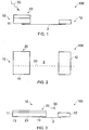
- Fig 1 illustrates an example of an apparatus 100 in cross-section.
- the apparatus 100 in this example, is an optoelectronic apparatus that has electrical characteristics that vary in the presence of photons 50.
- the apparatus 100 comprises graphene 2 and an asymmetric electrode arrangement 10 comprising a first electrode 11, a second electrode 12 separated from the first electrode across a portion of the graphene 2 and at least one surface plasmon polariton generator 20 associated with the first electrode 11.
- the surface plasmon polariton generator 20 couples incident photons 50 to surface plasmons associated with the first electrode 11.
- the photon-surface plasmon interaction propagates as a surface plasmon polariton to the graphene 2 where decoupling of the polariton and interaction of the photon and graphene occurs.
- the asymmetric electrode arrangement 10 results in a net change in the electrical characteristics of the graphene 2, which may be detected via the first electrode 11 and the second electrode 12.
- Fig 2 illustrates an example of an apparatus 100 in plan view from above.
- the apparatus 100 may be similar to the apparatus 100 described previously with reference to Fig 1 and similar references are used to denote similar features. The description of those features in relation to Fig 1 is also applicable to the features in Fig 2 .
- a virtual line 30 is illustrated that extends through the first electrode 11, the portion of graphene 2 between the first electrode 11 and the second electrode 12.
- the surface plasmon polariton generator 20 is configured to generate surface plasmon polaritons and to transport the generated surface plasmon polaritons to the graphene 2.
- the surface plasmon polariton generator is configured to provide a continuous plasma over at least several micrometers in a direction along the virtual line 30 through the first electrode 11, the graphene 2 and the second electrode 12.
- Continuous conductive material such as metal may be used to provide a continuous plasma.
- Fig 3 illustrates an example of an apparatus 100 in side view.
- the apparatus 100 may be similar to the apparatus 100 described previously with reference to Figs 1 and/or Fig 2 . Similar references are used to denote similar features. The description of those features in relation to Fig 1 and Fig 2 is also applicable to the features in Fig 3 .
- the plasmon polariton generator 20 is configured to generate surface plasmon polaritons and to transport the generated surface plasmon polaritons from a first area 13 to a second area 14.
- the first area 13 is part of the first electrode 11. It does not overlie exposed graphene 2. In some but not necessarily all examples, the first area 13 is not in physical or direct electrical contact with the graphene 2. It does not overlie the graphene 2.
- the second area 14 is part of the first electrode 11.
- the second area 14 is in direct electrical contact with the graphene 2 and may be in physical contact. It overlies the graphene 2.
- the plasmon polariton generator 20 may be configured to generate a continuous plasma form the first area 13 to the second area 14 in a direction parallel to the line 30 through the first electrode 11, the graphene 2 and the second electrode 12.
- the distance between the first area 13 and the second area 14 may, in some examples, be over several micrometers.
- Continuous conductive material 23 such as metal may be used to provide a continuous plasma.
- Figs 4A to 4C illustrate examples of plasmon polariton generators 20.
- the plasmon polariton generators 20 comprise optical couplers 40 in combination with continuous conductive material 23.
- the continuous conductive material 23 is part of the first electrode 11.
- a conductive path is provided along a continuous surface 22 of the first electrode 11.
- the conductive path may extend, as illustrated in Fig 3 , from the first area 13 to the second area 14.
- the optical coupler 40 may be associated with the first area 13 but not with the second area 14.
- the optical coupler 40 comprises a surface structure 25 that has periodicity in a direction parallel to the line 30.
- the surface structure 25 has a repeat pattern of period d nm.
- the surface structure 25, in this example, is a nanoscale structure and d ⁇ 1 ⁇ m.
- the surface structure 25 is continuous on a scale significantly larger than its period d and it may extend for at least several ⁇ m.
- the surface structure 25 may be formed by a periodic pattern, for example, undulations or channels 21, in an upper surface 22 of the conductive material 23 of the first electrode 11.
- the upper surface 22 of the conductive material 23 of the first electrode 11 has periodic profile modulations 21.
- the periodicity of the surface structure 25 is at least in a direction parallel to the line 30 through the first electrode 11, the graphene 2 and the second electrode 12.
- the surface structure 25 is a grating. It comprises alternate high and low profile portions.
- the grating 25 is a regular grating and all the high portions are of the same size and all of the low portions are of the same size.
- the high portions and low portions may be of the same size.
- the boundaries of the high and low profile portions are parallel to each other and extend orthogonally to the line 30.
- the repetition of the periodic surface structure 25, the periodicity, is in this example parallel to the line 30.
- the optical coupler 40 comprises a prism 28.
- the prism 28 contacts the conductive material 23 of the first electrode 11.
- the prism 28 is separated from the conductive material 23 of the first electrode 11 by a very small gap 29.
- a surface plasmon polariton generator 20 couples incident photons 50 with surface plasmons. This is achieved by matching the wave vector of the incident photon 50 to the wave vector of the surface plasmon.
- a wave vector is represented as two components (a, b), where a is the component parallel to an interface defined by the surface 22 of the conductive material 23 and b is the component orthogonal to that interface.
- the surface plasmon polariton generator 20 is configured to enable wave vector matching between the incident photon 50 and the surface plasmon.
- the surface plasmon polariton generator 20 is configured to impart a component of momentum (wave vector) to an incident photon 50 in at least a direction parallel to the line 30 through the first electrode 11, the graphene 2 and the second electrode 12 (i.e. parallel to the interface).
- asymmetry between the first electrode 11 and the second electrode 12 is achieved by associating a surface plasmon polariton generator 20 with the first electrode but not associating a surface plasmon polariton generator 20 with the second electrode 12.
- asymmetry in the asymmetrical electrode arrangement 10 may be achieved in other ways.
- the first electrode 11 may be associated with a first surface plasmon polariton generator 20 and the second electrode 12 may be associated with a second different surface plasmon polariton generator 20.
- the first surface plasmon polariton generator 20 may be configured to selectively couple photons of a first frequency and the second surface plasmon polariton generator 20 may be configured to selectively couple photons of a second frequency. In the illustrated example, this is achieved by using gratings 25 of different periods for the first surface plasmon polariton generator 20 and the second surface plasmon polariton generator 20.
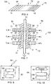
- Fig 7 illustrates an example of an apparatus 100 where the asymmetric electrode arrangement 10 comprises a plurality 70 of first electrodes 11, each of which is associated with a different surface plasmon polariton generator 20.
- the different surface plasmon polariton generators 20 may be configured to selectively couple photons of different particular frequencies. In the illustrated example, this is achieved by using gratings 25 of different periods for each of the first surface plasmon polariton generators 20.
- the second electrode 12 is a common electrode 72 separated from the plurality of first electrodes 11 by the graphene 2.
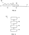
- Fig 8 illustrates an example of an asymmetric first electrode 11.
- the first electrode comprises a first portion 13 and a second portion 14.
- the first portion 13 provides the optical coupler 40 in the form of a periodic grating 25 which operates as the surface plasmon polariton generator 20 as described with reference to Fig 4A .
- the second portion 14 does not provide a periodic grating 25. It is flat. It operates to transport generated surface plasmon polaritons to the graphene 2.
- the second portion 14 is adjacent to the graphene 2 and the first portion 13 is not.
- the upper surface 60 of the second portion 14 may, in some examples, operate as a substrate for the adsorption of analyte.
- Fig 9 illustrates a narrowband photo detector 82.
- the apparatus 100 is used to detect a photon 50 of a particular frequency or photons 50 of particular frequencies depending upon implementation.
- a detector 80 is connected to the or each first electrode 11 and the second electrode 12 of the apparatus 100 and detects changes in the electrical characteristics of the graphene 2.
- the graphene may produce a photo-current dependent upon the number of incident photons 50 of the correct frequency at the surface plasmon polariton generator 20 associated with the or each first electrode 11.
- the 'correct' frequency is determined by the boundary conditions described with reference to Fig 5 .
- Fig 10 illustrates an analyte sensor 94.
- the apparatus 100 detects a photon 50 of a particular frequency or photons of particular frequencies depending upon implementation.
- a detector 80 is connected to the or each first electrode 11 and the second electrode 12 of the apparatus 100 and detects changes in the electrical characteristics of the graphene 2.
- the graphene may produce a photo-current dependent upon the number of incident photons 50 of the correct frequency at the surface plasmon polariton generator 20 associated with the or each first electrode 11.
- the 'correct' frequency is determined by the boundary conditions described with reference to Fig 5 .
- the analyte sensor 94 additionally comprises a source 90 of photons 50 at the correct frequency.
- the source 90 may be a narrowband source such as a laser or alternatively a light emitting diode.
- an analyte adsorbs to the exposed graphene 2 and/or the first electrode 11 adjacent to the graphene 2, there may be a change in how the electrical characteristics of the graphene 2 change with incident photons.
- the change in electrical characteristics may be calibrated against type and/or concentration of analyte.
- Fig 11 illustrates a method 110 comprising:
- the apparatus 10 may comprise: graphene 2; and an asymmetric electrode arrangement 10 comprising a first electrode 11, a second electrode 12 separated from the first electrode 11 across a portion of the graphene 2, wherein the first electrode 11 extends from a first area 13 that does not contact the graphene to a second area 14 that does contact the graphene, and wherein the first electrode 11 at the first area 13 is associated with an optical coupler 40.
- the optical coupler 40 may be configured to couple photons to surface plasmons to generate surface plasmon polaritons that are transported from the first area 13 to the second area 14.
- module' refers to a unit or apparatus that excludes certain parts/components that would be added by an end manufacturer or a user.
- the apparatus 100 may be a module.
- Non-bandgap semiconductors include semimetals.
- the semiconductor may be a bandgap semiconductor.
- the semiconductor may be a non-bandgap semiconductor.
- the semiconductor material is a material with a low density of electron states near the Fermi level, so that the amount of free carriers is too low to screen the collection field generated by the junction at the plasmon polariton generator.
Landscapes
- Engineering & Computer Science (AREA)
- Physics & Mathematics (AREA)
- Chemical & Material Sciences (AREA)
- Nanotechnology (AREA)
- Materials Engineering (AREA)
- General Physics & Mathematics (AREA)
- Condensed Matter Physics & Semiconductors (AREA)
- Crystallography & Structural Chemistry (AREA)
- Composite Materials (AREA)
- Optics & Photonics (AREA)
- Electromagnetism (AREA)
- Computer Networks & Wireless Communication (AREA)
- Signal Processing (AREA)
- Investigating Or Analysing Materials By Optical Means (AREA)
- Investigating, Analyzing Materials By Fluorescence Or Luminescence (AREA)
Description
- Embodiments of the present invention relate to an apparatus to detect incident photons.
- A photo-detector is an apparatus that has a measurable electrical characteristic that changes with incidence of photons. For example, a photo-detector may transduce a photon flux into an electrical current or voltage. Photo-detectors may use semiconductors. When an incident photon is absorbed, one or more electrons are raised to a higher energy level where they produce a photocurrent. The documents
EP1737047 ,WO2013074542 andUS20070235635 disclose known examples of photodetectors involving plasmonic structures. - The photodetection apparatus of the invention is defined in claim 1. According to various, but not necessarily all, embodiments of the invention there is provided an apparatus comprising: graphene; and an asymmetric electrode arrangement comprising a first electrode, a second electrode separated from the first electrode across a portion of the graphene and at least one surface plasmon polariton generator associated with at least the first electrode.
- For a better understanding of various examples that are useful for understanding the brief description, reference will now be made by way of example only to the accompanying drawings in which:
-
Fig 1 illustrates an example of the apparatus; -
Fig 2 illustrates another example of the apparatus; -
Fig 3 illustrates another example of the apparatus; -
Figs 4A to 4C illustrate examples of plasmon polariton generators; -
Fig 5 illustrates wave vector matching of an incident photon and a surface plasmon; -
Fig 6 illustrates another example of the apparatus; -
Fig 7 illustrates another example of the apparatus; -
Fig 8 illustrates an example of an asymmetric first electrode; -
Fig 9 illustrates a narrowband photo detector comprising the apparatus; -
Fig 10 illustrates an analyte sensor comprising the apparatus; and -
Fig 11 illustrates a method. - The Figures illustrate an
apparatus 100 comprising
semiconductor 2 and anasymmetric electrode arrangement 10 comprising afirst electrode 11, asecond electrode 12 separated from the first electrode across a portion of thesemiconductor 2 and at least one surfaceplasmon polariton generator 20 associated with thefirst electrode 11. - In the following description various examples of the
apparatus 100 are described, where thesemiconductor 2 is graphene. However, thesemiconductor 2 may, in other examples, be a different semiconductor. - The semiconductor is a two-dimensional (2) semiconductor such as graphene or molybdenum disulphide (MoS2)
- In some but not necessarily all examples, the
semiconductor 2 may have a low photon absorption. In some but not necessarily all examples, thesemiconductor 2 may have a high electron mobility. Thus in some but not necessarily all examples, thesemiconductor 2 may have an electron mobility greater than 5k cm2V-1s-1 and a photon absorption of less than 5% or 10%. -
Fig 1 illustrates an example of anapparatus 100 in cross-section. Theapparatus 100, in this example, is an optoelectronic apparatus that has electrical characteristics that vary in the presence ofphotons 50. - The
apparatus 100 comprisesgraphene 2 and anasymmetric electrode arrangement 10 comprising afirst electrode 11, asecond electrode 12 separated from the first electrode across a portion of thegraphene 2 and at least one surfaceplasmon polariton generator 20 associated with thefirst electrode 11. - The surface
plasmon polariton generator 20couples incident photons 50 to surface plasmons associated with thefirst electrode 11. The photon-surface plasmon interaction propagates as a surface plasmon polariton to thegraphene 2 where decoupling of the polariton and interaction of the photon and graphene occurs. - The
asymmetric electrode arrangement 10 results in a net change in the electrical characteristics of thegraphene 2, which may be detected via thefirst electrode 11 and thesecond electrode 12. -
Fig 2 illustrates an example of anapparatus 100 in plan view from above. Theapparatus 100 may be similar to theapparatus 100 described previously with reference toFig 1 and similar references are used to denote similar features. The description of those features in relation toFig 1 is also applicable to the features inFig 2 . - In
Fig 2 , avirtual line 30 is illustrated that extends through thefirst electrode 11, the portion ofgraphene 2 between thefirst electrode 11 and thesecond electrode 12. - The surface
plasmon polariton generator 20 is configured to generate surface plasmon polaritons and to transport the generated surface plasmon polaritons to thegraphene 2. - In order to transport the generated surface plasmon polaritons to the
graphene 2, the surface plasmon polariton generator is configured to provide a continuous plasma over at least several micrometers in a direction along thevirtual line 30 through thefirst electrode 11, thegraphene 2 and thesecond electrode 12. Continuous conductive material such as metal may be used to provide a continuous plasma. -
Fig 3 illustrates an example of anapparatus 100 in side view. Theapparatus 100 may be similar to theapparatus 100 described previously with reference toFigs 1 and/orFig 2 . Similar references are used to denote similar features. The description of those features in relation toFig 1 and Fig 2 is also applicable to the features inFig 3 . - In
Fig 3 , theplasmon polariton generator 20 is configured to generate surface plasmon polaritons and to transport the generated surface plasmon polaritons from afirst area 13 to asecond area 14. - The
first area 13 is part of thefirst electrode 11. It does not overlie exposedgraphene 2. In some but not necessarily all examples, thefirst area 13 is not in physical or direct electrical contact with thegraphene 2. It does not overlie thegraphene 2. - The
second area 14 is part of thefirst electrode 11. Thesecond area 14 is in direct electrical contact with thegraphene 2 and may be in physical contact. It overlies thegraphene 2. - In this example, the
plasmon polariton generator 20 may be configured to generate a continuous plasma form thefirst area 13 to thesecond area 14 in a direction parallel to theline 30 through thefirst electrode 11, thegraphene 2 and thesecond electrode 12. The distance between thefirst area 13 and thesecond area 14 may, in some examples, be over several micrometers. Continuousconductive material 23 such as metal may be used to provide a continuous plasma. -
Figs 4A to 4C illustrate examples ofplasmon polariton generators 20. In these examples, theplasmon polariton generators 20 compriseoptical couplers 40 in combination with continuousconductive material 23. The continuousconductive material 23 is part of thefirst electrode 11. - A conductive path is provided along a
continuous surface 22 of thefirst electrode 11. The conductive path may extend, as illustrated inFig 3 , from thefirst area 13 to thesecond area 14. - As illustrated in
Fig 8 , theoptical coupler 40 may be associated with thefirst area 13 but not with thesecond area 14. - In the example of
Fig 4A , theoptical coupler 40 comprises asurface structure 25 that has periodicity in a direction parallel to theline 30. - The
surface structure 25 has a repeat pattern of period d nm. Thesurface structure 25, in this example, is a nanoscale structure and d < 1µm. Thesurface structure 25 is continuous on a scale significantly larger than its period d and it may extend for at least several µm. - The
surface structure 25 may be formed by a periodic pattern, for example, undulations orchannels 21, in anupper surface 22 of theconductive material 23 of thefirst electrode 11. - In the illustrated example, the
upper surface 22 of theconductive material 23 of thefirst electrode 11 hasperiodic profile modulations 21. - The periodicity of the
surface structure 25 is at least in a direction parallel to theline 30 through thefirst electrode 11, thegraphene 2 and thesecond electrode 12. - In the illustrated example, the
surface structure 25 is a grating. It comprises alternate high and low profile portions. In this example, the grating 25 is a regular grating and all the high portions are of the same size and all of the low portions are of the same size. The high portions and low portions may be of the same size. - The boundaries of the high and low profile portions are parallel to each other and extend orthogonally to the
line 30. The repetition of theperiodic surface structure 25, the periodicity, is in this example parallel to theline 30. - In the examples of
Fig 4B and 4C , theoptical coupler 40 comprises aprism 28. InFig 4B , theprism 28 contacts theconductive material 23 of thefirst electrode 11. InFig 4C , theprism 28 is separated from theconductive material 23 of thefirst electrode 11 by a verysmall gap 29. - As illustrated in
Fig 5 , a surfaceplasmon polariton generator 20couples incident photons 50 with surface plasmons. This is achieved by matching the wave vector of theincident photon 50 to the wave vector of the surface plasmon. - In the simple example of
Fig 5 a wave vector is represented as two components (a, b), where a is the component parallel to an interface defined by thesurface 22 of theconductive material 23 and b is the component orthogonal to that interface. - If we assume that the
conductive material 23 has a dielectric constant ε2, and that the dielectric material (e.g. air) adjacent to the interface has dielectric constant ε1, then the boundary conditions for coupling of the surface plasmon polariton and the incident photon are:


- The surface
plasmon polariton generator 20 is configured to enable wave vector matching between theincident photon 50 and the surface plasmon. The surfaceplasmon polariton generator 20 is configured to impart a component of momentum (wave vector) to anincident photon 50 in at least a direction parallel to theline 30 through thefirst electrode 11, thegraphene 2 and the second electrode 12 (i.e. parallel to the interface). - Referring back to the example illustrated in
Fig 3 . In this example, asymmetry between thefirst electrode 11 and thesecond electrode 12 is achieved by associating a surfaceplasmon polariton generator 20 with the first electrode but not associating a surfaceplasmon polariton generator 20 with thesecond electrode 12. - However, asymmetry in the
asymmetrical electrode arrangement 10 may be achieved in other ways. - For example, as illustrated in
Fig 6 , thefirst electrode 11 may be associated with a first surfaceplasmon polariton generator 20 and thesecond electrode 12 may be associated with a second different surfaceplasmon polariton generator 20. - For example, the first surface
plasmon polariton generator 20 may be configured to selectively couple photons of a first frequency and the second surfaceplasmon polariton generator 20 may be configured to selectively couple photons of a second frequency. In the illustrated example, this is achieved by usinggratings 25 of different periods for the first surfaceplasmon polariton generator 20 and the second surfaceplasmon polariton generator 20. -
Fig 7 illustrates an example of anapparatus 100 where theasymmetric electrode arrangement 10 comprises aplurality 70 offirst electrodes 11, each of which is associated with a different surfaceplasmon polariton generator 20. The different surfaceplasmon polariton generators 20 may be configured to selectively couple photons of different particular frequencies. In the illustrated example, this is achieved by usinggratings 25 of different periods for each of the first surfaceplasmon polariton generators 20. - In the example of
Fig 7 , thesecond electrode 12 is acommon electrode 72 separated from the plurality offirst electrodes 11 by thegraphene 2. -
Fig 8 illustrates an example of an asymmetricfirst electrode 11. The first electrode comprises afirst portion 13 and asecond portion 14. Thefirst portion 13 provides theoptical coupler 40 in the form of aperiodic grating 25 which operates as the surfaceplasmon polariton generator 20 as described with reference toFig 4A . Thesecond portion 14 does not provide aperiodic grating 25. It is flat. It operates to transport generated surface plasmon polaritons to thegraphene 2. In this example, thesecond portion 14 is adjacent to thegraphene 2 and thefirst portion 13 is not. - The
upper surface 60 of thesecond portion 14 may, in some examples, operate as a substrate for the adsorption of analyte. -
Fig 9 illustrates anarrowband photo detector 82. Theapparatus 100 is used to detect aphoton 50 of a particular frequency orphotons 50 of particular frequencies depending upon implementation. - A
detector 80 is connected to the or eachfirst electrode 11 and thesecond electrode 12 of theapparatus 100 and detects changes in the electrical characteristics of thegraphene 2. For example, the graphene may produce a photo-current dependent upon the number ofincident photons 50 of the correct frequency at the surfaceplasmon polariton generator 20 associated with the or eachfirst electrode 11. The 'correct' frequency is determined by the boundary conditions described with reference toFig 5 . -
Fig 10 illustrates ananalyte sensor 94. - The
apparatus 100 detects aphoton 50 of a particular frequency or photons of particular frequencies depending upon implementation. - A
detector 80 is connected to the or eachfirst electrode 11 and thesecond electrode 12 of theapparatus 100 and detects changes in the electrical characteristics of thegraphene 2. For example, the graphene may produce a photo-current dependent upon the number ofincident photons 50 of the correct frequency at the surfaceplasmon polariton generator 20 associated with the or eachfirst electrode 11. The 'correct' frequency is determined by the boundary conditions described with reference toFig 5 . - The
analyte sensor 94 additionally comprises asource 90 ofphotons 50 at the correct frequency. Thesource 90 may be a narrowband source such as a laser or alternatively a light emitting diode. - When an analyte adsorbs to the exposed
graphene 2 and/or thefirst electrode 11 adjacent to thegraphene 2, there may be a change in how the electrical characteristics of thegraphene 2 change with incident photons. The change in electrical characteristics may be calibrated against type and/or concentration of analyte. -
Fig 11 illustrates amethod 110 comprising: - at
block 111 providing anasymmetric electrode arrangement 10 comprising afirst electrode 11 and asecond electrode 12 separated from the first electrode across a portion of thegraphene 2, - at
block 112 providing anoptical coupler 40 at at least afirst area 13 of thefirst electrode 11; - at
block 113 providing a conductive path along a surface of thefirst electrode 11 adjacent to a dielectric from thefirst area 13 of the first electrode to asecond area 14 of thefirst electrode 11 that contacts thegraphene 2; - at
block 114 detecting electrical characteristics of thegraphene 2 using thefirst electrode 11 and thesecond electrode 12. - It will be appreciated from the described examples, that the
apparatus 10 may comprise:graphene 2; and anasymmetric electrode arrangement 10 comprising afirst electrode 11, asecond electrode 12 separated from thefirst electrode 11 across a portion of thegraphene 2, wherein thefirst electrode 11 extends from afirst area 13 that does not contact the graphene to asecond area 14 that does contact the graphene, and wherein thefirst electrode 11 at thefirst area 13 is associated with an optical coupler 40.Theoptical coupler 40 may be configured to couple photons to surface plasmons to generate surface plasmon polaritons that are transported from thefirst area 13 to thesecond area 14. - As used here 'module' refers to a unit or apparatus that excludes certain parts/components that would be added by an end manufacturer or a user. The
apparatus 100 may be a module. - The term 'comprise' is used in this document with an inclusive not an exclusive meaning. That is any reference to X comprising Y indicates that X may comprise only one Y or may comprise more than one Y. If it is intended to use 'comprise' with an exclusive meaning then it will be made clear in the context by referring to "comprising only one" or by using "consisting".
- In this brief description, reference has been made to various examples. The description of features or functions in relation to an example indicates that those features or functions are present in that example. The use of the term 'example' or 'for example' or 'may' in the text denotes, whether explicitly stated or not, that such features or functions are present in at least the described example, whether described as an example or not, and that they can be, but are not necessarily, present in some of or all other examples. Thus 'example', 'for example' or 'may' refers to a particular instance in a class of examples. A property of the instance can be a property of only that instance or a property of the class or a property of a sub-class of the class that includes some but not all of the instances in the class.
- Although embodiments of the present invention have been described in the preceding paragraphs with reference to various examples, it should be appreciated that modifications to the examples given can be made without departing from the scope of the invention as claimed.
- Semiconductor in this document includes bandgap semiconductors, which have a bandgap, and non-band gap semiconductors, which do not have a bandgap. Non-bandgap semiconductors include semimetals. In some but not necessarily all of the preceding examples, the semiconductor may be a bandgap semiconductor. In some but not necessarily all of the preceding examples, the semiconductor may be a non-bandgap semiconductor.
- The semiconductor material is a material with a low density of electron states near the Fermi level, so that the amount of free carriers is too low to screen the collection field generated by the junction at the plasmon polariton generator.
- Features described in the preceding description may be used in combinations other than the combinations explicitly described.
- Although functions have been described with reference to certain features, those functions may be performable by other features whether described or not.
- Although features have been described with reference to certain embodiments, those features may also be present in other embodiments whether described or not.
- Whilst endeavoring in the foregoing specification to draw attention to those features of the invention believed to be of particular importance it should be understood that the Applicant claims protection in respect of any patentable feature or combination of features hereinbefore referred to and/or shown in the drawings whether or not particular emphasis has been placed thereon.
Claims (15)
- A photodetection apparatus (100) comprising:a two-dimensional semiconductor (2), andan asymmetric electrode arrangement (10) comprising a first electrode (11), a second electrode (12) separated from the first electrode (11) across a portion of the two-dimensional semiconductor (2) and at least one surface plasmon polariton generator (20) associated with at least the first electrode (11).
- A photodetection apparatus as claimed in claim 1, wherein the surface plasmon polariton generator is configured to impart a component of momentum to an incident photon in at least a direction parallel to the line through the first electrode, the two-dimensional semiconductor portion and the second electrode.
- A photodetection apparatus as claimed in claim 2, wherein the surface plasmon polariton generator is configured to impart a component of momentum to an incident photon preferentially in the direction parallel to the line through the first electrode, the two-dimensional semiconductor portion and the second electrode.
- A photodetection apparatus as claimed in any preceding claim, wherein the surface plasmon polariton generator is configured to generate surface plasmon polaritons and to transport the generated surface plasmon polaritons to the two-dimensional semiconductor.
- A photodetection apparatus as claimed in any preceding claim, wherein the surface plasmon polariton generator is configured to provide a continuous plasma over at least several micrometers in a direction along the line through the first electrode, the two-dimensional semiconductor portion and the second electrode.
- A photodetection apparatus as claimed in any preceding claim, wherein the surface plasmon polariton generator is configured to provide a continuous plasma from an area that is not contacting the two-dimensional semiconductor to an area that is contacting the two-dimensional semiconductor.
- A photodetection apparatus as claimed in any preceding claim, wherein the surface plasmon polariton generator is configured to provide continuous metal from an area that does not contact the two-dimensional semiconductor to an area that does contact the two-dimensional semiconductor.
- A photodetection apparatus as claimed in any preceding claim, wherein the surface plasmon polariton generator comprises a periodic structure having a periodicity, wherein the periodicity is at least in a direction parallel to the line through the first electrode, the two-dimensional semiconductor portion and the second electrode.
- A photodetection apparatus as claimed in any preceding claim, wherein the surface plasmon polariton generator comprises a periodic structure having a periodicity, wherein the periodicity is parallel to the line through the first electrode, the two-dimensional semiconductor portion and the second electrode.
- A photodetection apparatus as claimed in any preceding claim, wherein the two-dimensional semiconductor is graphene or molybdenum disulphide.
- A photodetection apparatus as claimed in any preceding claim, wherein surface plasmon polariton generator comprises conductive material comprising a surface, wherein the surface is continuous and comprises periodic profile modulations.
- A photodetection apparatus as claimed in any preceding claim, wherein the first electrode is associated with a surface plasmon polariton generator but the second electrode is not associated with a surface plasmon polariton generator.
- A photodetection apparatus as claimed in any of claims 1 to 11, wherein the first electrode is associated with a surface plasmon polariton generator for selectively coupling photons of a first frequency and the second electrode is associated with a surface plasmon polariton generator for selectively coupling photons of a second frequency, different to the first frequency.
- A photodetection apparatus as claimed in any preceding claim, wherein the asymmetric electrode arrangement comprises a plurality of first electrodes, each of which is associated with a surface plasmon polariton generator for selectively coupling photons of a particular frequency.
- A photodetection apparatus as claimed in claim 14, wherein the second electrode is a common electrode separated from the plurality of first electrodes by the two-dimensional semiconductor.
Applications Claiming Priority (2)
| Application Number | Priority Date | Filing Date | Title |
|---|---|---|---|
| GR20130100631 | 2013-11-05 | ||
| PCT/FI2014/050071 WO2015067843A1 (en) | 2013-11-05 | 2014-01-29 | An apparatus and a method for detecting photons |
Publications (3)
| Publication Number | Publication Date |
|---|---|
| EP3066694A1 EP3066694A1 (en) | 2016-09-14 |
| EP3066694A4 EP3066694A4 (en) | 2017-08-02 |
| EP3066694B1 true EP3066694B1 (en) | 2020-10-14 |
Family
ID=53040949
Family Applications (1)
| Application Number | Title | Priority Date | Filing Date |
|---|---|---|---|
| EP14860362.4A Active EP3066694B1 (en) | 2013-11-05 | 2014-01-29 | A photodetection apparatus |
Country Status (4)
| Country | Link |
|---|---|
| US (1) | US20160254398A1 (en) |
| EP (1) | EP3066694B1 (en) |
| CN (1) | CN105765732B (en) |
| WO (1) | WO2015067843A1 (en) |
Families Citing this family (3)
| Publication number | Priority date | Publication date | Assignee | Title |
|---|---|---|---|---|
| WO2016121408A1 (en) * | 2015-01-28 | 2016-08-04 | 三菱電機株式会社 | Electromagnetic wave detector and electromagnetic wave detector array |
| CN106653930B (en) * | 2016-09-13 | 2018-09-25 | 北京大学 | Phasmon enhancing photodetector based on semiconductor nano material and preparation method thereof |
| US10193638B2 (en) * | 2016-09-30 | 2019-01-29 | The Trustees Of Boston College | Wireless communication system via nanoscale plasmonic antennas |
Family Cites Families (9)
| Publication number | Priority date | Publication date | Assignee | Title |
|---|---|---|---|---|
| US7330666B1 (en) * | 2003-01-31 | 2008-02-12 | Ciena Corporation | Method and apparatus for controlling modulator phase alignment in a transmitter of an optical communications system |
| US7423254B2 (en) * | 2004-03-22 | 2008-09-09 | Research Foundation Of The City University Of New York | High responsivity high bandwidth metal-semiconductor-metal optoelectronic device |
| ATE499705T1 (en) * | 2004-04-05 | 2011-03-15 | Nec Corp | PHOTODIODE AND PRODUCTION METHOD THEREOF |
| US7817278B2 (en) * | 2007-08-08 | 2010-10-19 | Agilent Technologies, Inc. | Surface plasmon resonance sensor apparatus having multiple dielectric layers |
| US8247881B2 (en) * | 2009-04-27 | 2012-08-21 | University Of Seoul Industry Cooperation Foundation | Photodiodes with surface plasmon couplers |
| JP5660991B2 (en) * | 2010-09-16 | 2015-01-28 | 三菱電機株式会社 | Photoelectric conversion element and image sensor |
| JP2015502658A (en) * | 2011-11-14 | 2015-01-22 | パシフィック インテグレイテッド エナジー, インコーポレイテッド | Devices, systems, and methods for electromagnetic energy collection |
| JP5871829B2 (en) * | 2012-03-06 | 2016-03-01 | 三菱電機株式会社 | Photoelectric conversion element and photoelectric conversion element array |
| JP6161554B2 (en) * | 2013-04-26 | 2017-07-12 | 三菱電機株式会社 | Electromagnetic wave detector and electromagnetic wave detector array |
-
2014
- 2014-01-29 WO PCT/FI2014/050071 patent/WO2015067843A1/en not_active Ceased
- 2014-01-29 EP EP14860362.4A patent/EP3066694B1/en active Active
- 2014-01-29 CN CN201480060842.4A patent/CN105765732B/en active Active
- 2014-01-29 US US15/032,372 patent/US20160254398A1/en not_active Abandoned
Non-Patent Citations (1)
| Title |
|---|
| None * |
Also Published As
| Publication number | Publication date |
|---|---|
| CN105765732A (en) | 2016-07-13 |
| US20160254398A1 (en) | 2016-09-01 |
| CN105765732B (en) | 2019-04-09 |
| WO2015067843A1 (en) | 2015-05-14 |
| EP3066694A1 (en) | 2016-09-14 |
| EP3066694A4 (en) | 2017-08-02 |
Similar Documents
| Publication | Publication Date | Title |
|---|---|---|
| Urich et al. | Intrinsic response time of graphene photodetectors | |
| Bhattacharya et al. | Beyond 30% conversion efficiency in silicon solar cells: a numerical demonstration | |
| Lin et al. | Silicon-based broadband antenna for high responsivity and polarization-insensitive photodetection at telecommunication wavelengths | |
| CN103811568B (en) | The incident graphene photodetector in a kind of surface based on one-dimensional grating | |
| Kim et al. | Whispering gallery modes enhance the near-infrared photoresponse of hourglass-shaped silicon nanowire photodiodes | |
| JP5094385B2 (en) | High response high bandwidth metal-semiconductor-metal photoelectric device | |
| Walker et al. | Nonradiative lifetime extraction using power-dependent relative photoluminescence of III-V semiconductor double-heterostructures | |
| Nusir et al. | Near-infrared metal-semiconductor-metal photodetector based on semi-insulating GaAs and interdigital electrodes | |
| Kim et al. | Self-powered silicon metal–semiconductor–metal photodetector based on asymmetric Schottky barrier heights | |
| Park et al. | Plasmonic nanoparticles on graphene absorber for broadband high responsivity 2D/3D photodiode | |
| Yamada et al. | Modeling of nanohole silicon pin/nip photodetectors: Steady state and transient characteristics | |
| KR102189605B1 (en) | Optical detector | |
| US20160254398A1 (en) | An apparatus and a method for detecting photons | |
| Wang et al. | Patterned 3D-graphene for self-powered broadband photodetector | |
| Marouf et al. | The effect of different nanoparticles surface plasmon polariton (SPP) grating on Ge, Si, InP, and GaAs photodetectors performance | |
| Dang et al. | The fabrication and characterization of flexible single-crystalline silicon and germanium p-intrinsic-n photodetectors on plastic substrates | |
| US8604574B2 (en) | Transparent photodetector | |
| Tang et al. | Photoresponse enhancement in graphene/silicon infrared detector by controlling photocarrier collection | |
| Qiu et al. | High performance of a broadband room-temperature Si detector beyond the cut-off wavelength | |
| CN106803528A (en) | Position sensitive photo-detector based on Graphene | |
| CN106252454B (en) | A kind of photodetector and Electro-Optical Sensor Set | |
| Arefinia | Analytical modeling for plasmonic graphene/GaAs solar cells with random distribution of nonuniform-sized nanoparticles | |
| Yanilmaz et al. | Graphene/SOI-based self-powered Schottky barrier photodiode array | |
| Zhang et al. | Conformal TCO-semiconductor-metal nanowire array for narrowband and polarization-insensitive hot-electron photodetection application | |
| CN110224068A (en) | A photodetection structure based on perovskite nanowires |
Legal Events
| Date | Code | Title | Description |
|---|---|---|---|
| PUAI | Public reference made under article 153(3) epc to a published international application that has entered the european phase |
Free format text: ORIGINAL CODE: 0009012 |
|
| 17P | Request for examination filed |
Effective date: 20160510 |
|
| AK | Designated contracting states |
Kind code of ref document: A1 Designated state(s): AL AT BE BG CH CY CZ DE DK EE ES FI FR GB GR HR HU IE IS IT LI LT LU LV MC MK MT NL NO PL PT RO RS SE SI SK SM TR |
|
| AX | Request for extension of the european patent |
Extension state: BA ME |
|
| DAX | Request for extension of the european patent (deleted) | ||
| A4 | Supplementary search report drawn up and despatched |
Effective date: 20170629 |
|
| RIC1 | Information provided on ipc code assigned before grant |
Ipc: H01L 31/0232 20140101ALI20170623BHEP Ipc: B82Y 30/00 20110101ALI20170623BHEP Ipc: H01L 31/0224 20060101AFI20170623BHEP Ipc: G02B 6/122 20060101ALI20170623BHEP Ipc: H01L 31/0256 20060101ALI20170623BHEP |
|
| RAP1 | Party data changed (applicant data changed or rights of an application transferred) |
Owner name: NOKIA TECHNOLOGIES OY |
|
| GRAP | Despatch of communication of intention to grant a patent |
Free format text: ORIGINAL CODE: EPIDOSNIGR1 |
|
| STAA | Information on the status of an ep patent application or granted ep patent |
Free format text: STATUS: GRANT OF PATENT IS INTENDED |
|
| INTG | Intention to grant announced |
Effective date: 20200520 |
|
| GRAS | Grant fee paid |
Free format text: ORIGINAL CODE: EPIDOSNIGR3 |
|
| GRAA | (expected) grant |
Free format text: ORIGINAL CODE: 0009210 |
|
| STAA | Information on the status of an ep patent application or granted ep patent |
Free format text: STATUS: THE PATENT HAS BEEN GRANTED |
|
| AK | Designated contracting states |
Kind code of ref document: B1 Designated state(s): AL AT BE BG CH CY CZ DE DK EE ES FI FR GB GR HR HU IE IS IT LI LT LU LV MC MK MT NL NO PL PT RO RS SE SI SK SM TR |
|
| REG | Reference to a national code |
Ref country code: GB Ref legal event code: FG4D |
|
| REG | Reference to a national code |
Ref country code: AT Ref legal event code: REF Ref document number: 1324429 Country of ref document: AT Kind code of ref document: T Effective date: 20201015 Ref country code: CH Ref legal event code: EP |
|
| REG | Reference to a national code |
Ref country code: DE Ref legal event code: R096 Ref document number: 602014071310 Country of ref document: DE |
|
| REG | Reference to a national code |
Ref country code: IE Ref legal event code: FG4D |
|
| REG | Reference to a national code |
Ref country code: AT Ref legal event code: MK05 Ref document number: 1324429 Country of ref document: AT Kind code of ref document: T Effective date: 20201014 |
|
| REG | Reference to a national code |
Ref country code: NL Ref legal event code: MP Effective date: 20201014 |
|
| PG25 | Lapsed in a contracting state [announced via postgrant information from national office to epo] |
Ref country code: GR Free format text: LAPSE BECAUSE OF FAILURE TO SUBMIT A TRANSLATION OF THE DESCRIPTION OR TO PAY THE FEE WITHIN THE PRESCRIBED TIME-LIMIT Effective date: 20210115 Ref country code: PT Free format text: LAPSE BECAUSE OF FAILURE TO SUBMIT A TRANSLATION OF THE DESCRIPTION OR TO PAY THE FEE WITHIN THE PRESCRIBED TIME-LIMIT Effective date: 20210215 Ref country code: NL Free format text: LAPSE BECAUSE OF FAILURE TO SUBMIT A TRANSLATION OF THE DESCRIPTION OR TO PAY THE FEE WITHIN THE PRESCRIBED TIME-LIMIT Effective date: 20201014 Ref country code: NO Free format text: LAPSE BECAUSE OF FAILURE TO SUBMIT A TRANSLATION OF THE DESCRIPTION OR TO PAY THE FEE WITHIN THE PRESCRIBED TIME-LIMIT Effective date: 20210114 Ref country code: FI Free format text: LAPSE BECAUSE OF FAILURE TO SUBMIT A TRANSLATION OF THE DESCRIPTION OR TO PAY THE FEE WITHIN THE PRESCRIBED TIME-LIMIT Effective date: 20201014 Ref country code: RS Free format text: LAPSE BECAUSE OF FAILURE TO SUBMIT A TRANSLATION OF THE DESCRIPTION OR TO PAY THE FEE WITHIN THE PRESCRIBED TIME-LIMIT Effective date: 20201014 |
|
| REG | Reference to a national code |
Ref country code: LT Ref legal event code: MG4D |
|
| PG25 | Lapsed in a contracting state [announced via postgrant information from national office to epo] |
Ref country code: BG Free format text: LAPSE BECAUSE OF FAILURE TO SUBMIT A TRANSLATION OF THE DESCRIPTION OR TO PAY THE FEE WITHIN THE PRESCRIBED TIME-LIMIT Effective date: 20210114 Ref country code: ES Free format text: LAPSE BECAUSE OF FAILURE TO SUBMIT A TRANSLATION OF THE DESCRIPTION OR TO PAY THE FEE WITHIN THE PRESCRIBED TIME-LIMIT Effective date: 20201014 Ref country code: AT Free format text: LAPSE BECAUSE OF FAILURE TO SUBMIT A TRANSLATION OF THE DESCRIPTION OR TO PAY THE FEE WITHIN THE PRESCRIBED TIME-LIMIT Effective date: 20201014 Ref country code: LV Free format text: LAPSE BECAUSE OF FAILURE TO SUBMIT A TRANSLATION OF THE DESCRIPTION OR TO PAY THE FEE WITHIN THE PRESCRIBED TIME-LIMIT Effective date: 20201014 Ref country code: SE Free format text: LAPSE BECAUSE OF FAILURE TO SUBMIT A TRANSLATION OF THE DESCRIPTION OR TO PAY THE FEE WITHIN THE PRESCRIBED TIME-LIMIT Effective date: 20201014 Ref country code: PL Free format text: LAPSE BECAUSE OF FAILURE TO SUBMIT A TRANSLATION OF THE DESCRIPTION OR TO PAY THE FEE WITHIN THE PRESCRIBED TIME-LIMIT Effective date: 20201014 Ref country code: IS Free format text: LAPSE BECAUSE OF FAILURE TO SUBMIT A TRANSLATION OF THE DESCRIPTION OR TO PAY THE FEE WITHIN THE PRESCRIBED TIME-LIMIT Effective date: 20210214 |
|
| PG25 | Lapsed in a contracting state [announced via postgrant information from national office to epo] |
Ref country code: HR Free format text: LAPSE BECAUSE OF FAILURE TO SUBMIT A TRANSLATION OF THE DESCRIPTION OR TO PAY THE FEE WITHIN THE PRESCRIBED TIME-LIMIT Effective date: 20201014 |
|
| REG | Reference to a national code |
Ref country code: DE Ref legal event code: R097 Ref document number: 602014071310 Country of ref document: DE |
|
| PG25 | Lapsed in a contracting state [announced via postgrant information from national office to epo] |
Ref country code: SM Free format text: LAPSE BECAUSE OF FAILURE TO SUBMIT A TRANSLATION OF THE DESCRIPTION OR TO PAY THE FEE WITHIN THE PRESCRIBED TIME-LIMIT Effective date: 20201014 Ref country code: EE Free format text: LAPSE BECAUSE OF FAILURE TO SUBMIT A TRANSLATION OF THE DESCRIPTION OR TO PAY THE FEE WITHIN THE PRESCRIBED TIME-LIMIT Effective date: 20201014 Ref country code: CZ Free format text: LAPSE BECAUSE OF FAILURE TO SUBMIT A TRANSLATION OF THE DESCRIPTION OR TO PAY THE FEE WITHIN THE PRESCRIBED TIME-LIMIT Effective date: 20201014 Ref country code: SK Free format text: LAPSE BECAUSE OF FAILURE TO SUBMIT A TRANSLATION OF THE DESCRIPTION OR TO PAY THE FEE WITHIN THE PRESCRIBED TIME-LIMIT Effective date: 20201014 Ref country code: RO Free format text: LAPSE BECAUSE OF FAILURE TO SUBMIT A TRANSLATION OF THE DESCRIPTION OR TO PAY THE FEE WITHIN THE PRESCRIBED TIME-LIMIT Effective date: 20201014 Ref country code: LT Free format text: LAPSE BECAUSE OF FAILURE TO SUBMIT A TRANSLATION OF THE DESCRIPTION OR TO PAY THE FEE WITHIN THE PRESCRIBED TIME-LIMIT Effective date: 20201014 |
|
| PLBE | No opposition filed within time limit |
Free format text: ORIGINAL CODE: 0009261 |
|
| STAA | Information on the status of an ep patent application or granted ep patent |
Free format text: STATUS: NO OPPOSITION FILED WITHIN TIME LIMIT |
|
| PG25 | Lapsed in a contracting state [announced via postgrant information from national office to epo] |
Ref country code: MC Free format text: LAPSE BECAUSE OF FAILURE TO SUBMIT A TRANSLATION OF THE DESCRIPTION OR TO PAY THE FEE WITHIN THE PRESCRIBED TIME-LIMIT Effective date: 20201014 Ref country code: DK Free format text: LAPSE BECAUSE OF FAILURE TO SUBMIT A TRANSLATION OF THE DESCRIPTION OR TO PAY THE FEE WITHIN THE PRESCRIBED TIME-LIMIT Effective date: 20201014 |
|
| REG | Reference to a national code |
Ref country code: CH Ref legal event code: PL |
|
| 26N | No opposition filed |
Effective date: 20210715 |
|
| GBPC | Gb: european patent ceased through non-payment of renewal fee |
Effective date: 20210129 |
|
| PG25 | Lapsed in a contracting state [announced via postgrant information from national office to epo] |
Ref country code: LU Free format text: LAPSE BECAUSE OF NON-PAYMENT OF DUE FEES Effective date: 20210129 |
|
| REG | Reference to a national code |
Ref country code: BE Ref legal event code: MM Effective date: 20210131 |
|
| PG25 | Lapsed in a contracting state [announced via postgrant information from national office to epo] |
Ref country code: IT Free format text: LAPSE BECAUSE OF FAILURE TO SUBMIT A TRANSLATION OF THE DESCRIPTION OR TO PAY THE FEE WITHIN THE PRESCRIBED TIME-LIMIT Effective date: 20201014 Ref country code: FR Free format text: LAPSE BECAUSE OF NON-PAYMENT OF DUE FEES Effective date: 20210131 Ref country code: AL Free format text: LAPSE BECAUSE OF FAILURE TO SUBMIT A TRANSLATION OF THE DESCRIPTION OR TO PAY THE FEE WITHIN THE PRESCRIBED TIME-LIMIT Effective date: 20201014 |
|
| PG25 | Lapsed in a contracting state [announced via postgrant information from national office to epo] |
Ref country code: LI Free format text: LAPSE BECAUSE OF NON-PAYMENT OF DUE FEES Effective date: 20210131 Ref country code: CH Free format text: LAPSE BECAUSE OF NON-PAYMENT OF DUE FEES Effective date: 20210131 Ref country code: GB Free format text: LAPSE BECAUSE OF NON-PAYMENT OF DUE FEES Effective date: 20210129 Ref country code: SI Free format text: LAPSE BECAUSE OF FAILURE TO SUBMIT A TRANSLATION OF THE DESCRIPTION OR TO PAY THE FEE WITHIN THE PRESCRIBED TIME-LIMIT Effective date: 20201014 |
|
| PG25 | Lapsed in a contracting state [announced via postgrant information from national office to epo] |
Ref country code: IE Free format text: LAPSE BECAUSE OF NON-PAYMENT OF DUE FEES Effective date: 20210129 |
|
| PG25 | Lapsed in a contracting state [announced via postgrant information from national office to epo] |
Ref country code: IS Free format text: LAPSE BECAUSE OF FAILURE TO SUBMIT A TRANSLATION OF THE DESCRIPTION OR TO PAY THE FEE WITHIN THE PRESCRIBED TIME-LIMIT Effective date: 20210214 |
|
| PG25 | Lapsed in a contracting state [announced via postgrant information from national office to epo] |
Ref country code: BE Free format text: LAPSE BECAUSE OF NON-PAYMENT OF DUE FEES Effective date: 20210131 |
|
| PG25 | Lapsed in a contracting state [announced via postgrant information from national office to epo] |
Ref country code: HU Free format text: LAPSE BECAUSE OF FAILURE TO SUBMIT A TRANSLATION OF THE DESCRIPTION OR TO PAY THE FEE WITHIN THE PRESCRIBED TIME-LIMIT; INVALID AB INITIO Effective date: 20140129 |
|
| PG25 | Lapsed in a contracting state [announced via postgrant information from national office to epo] |
Ref country code: CY Free format text: LAPSE BECAUSE OF FAILURE TO SUBMIT A TRANSLATION OF THE DESCRIPTION OR TO PAY THE FEE WITHIN THE PRESCRIBED TIME-LIMIT Effective date: 20201014 |
|
| P01 | Opt-out of the competence of the unified patent court (upc) registered |
Effective date: 20230527 |
|
| PG25 | Lapsed in a contracting state [announced via postgrant information from national office to epo] |
Ref country code: MK Free format text: LAPSE BECAUSE OF FAILURE TO SUBMIT A TRANSLATION OF THE DESCRIPTION OR TO PAY THE FEE WITHIN THE PRESCRIBED TIME-LIMIT Effective date: 20201014 |
|
| PG25 | Lapsed in a contracting state [announced via postgrant information from national office to epo] |
Ref country code: TR Free format text: LAPSE BECAUSE OF FAILURE TO SUBMIT A TRANSLATION OF THE DESCRIPTION OR TO PAY THE FEE WITHIN THE PRESCRIBED TIME-LIMIT Effective date: 20201014 |
|
| PG25 | Lapsed in a contracting state [announced via postgrant information from national office to epo] |
Ref country code: MT Free format text: LAPSE BECAUSE OF FAILURE TO SUBMIT A TRANSLATION OF THE DESCRIPTION OR TO PAY THE FEE WITHIN THE PRESCRIBED TIME-LIMIT Effective date: 20201014 |
|
| REG | Reference to a national code |
Ref country code: DE Ref legal event code: R079 Ref document number: 602014071310 Country of ref document: DE Free format text: PREVIOUS MAIN CLASS: H01L0031022400 Ipc: H10F0077200000 |
|
| PGFP | Annual fee paid to national office [announced via postgrant information from national office to epo] |
Ref country code: DE Payment date: 20251203 Year of fee payment: 13 |