EP3065181A1 - Spin control mechanism and spin device - Google Patents
Spin control mechanism and spin device Download PDFInfo
- Publication number
- EP3065181A1 EP3065181A1 EP14857027.8A EP14857027A EP3065181A1 EP 3065181 A1 EP3065181 A1 EP 3065181A1 EP 14857027 A EP14857027 A EP 14857027A EP 3065181 A1 EP3065181 A1 EP 3065181A1
- Authority
- EP
- European Patent Office
- Prior art keywords
- spin
- channel portion
- magnetic moment
- layer
- channel
- Prior art date
- Legal status (The legal status is an assumption and is not a legal conclusion. Google has not performed a legal analysis and makes no representation as to the accuracy of the status listed.)
- Granted
Links
Images




Classifications
-
- H—ELECTRICITY
- H10—SEMICONDUCTOR DEVICES; ELECTRIC SOLID-STATE DEVICES NOT OTHERWISE PROVIDED FOR
- H10N—ELECTRIC SOLID-STATE DEVICES NOT OTHERWISE PROVIDED FOR
- H10N50/00—Galvanomagnetic devices
- H10N50/80—Constructional details
-
- B—PERFORMING OPERATIONS; TRANSPORTING
- B81—MICROSTRUCTURAL TECHNOLOGY
- B81B—MICROSTRUCTURAL DEVICES OR SYSTEMS, e.g. MICROMECHANICAL DEVICES
- B81B5/00—Devices comprising elements which are movable in relation to each other, e.g. comprising slidable or rotatable elements
-
- H—ELECTRICITY
- H02—GENERATION; CONVERSION OR DISTRIBUTION OF ELECTRIC POWER
- H02K—DYNAMO-ELECTRIC MACHINES
- H02K49/00—Dynamo-electric clutches; Dynamo-electric brakes
- H02K49/06—Dynamo-electric clutches; Dynamo-electric brakes of the synchronous type
-
- H—ELECTRICITY
- H10—SEMICONDUCTOR DEVICES; ELECTRIC SOLID-STATE DEVICES NOT OTHERWISE PROVIDED FOR
- H10D—INORGANIC ELECTRIC SEMICONDUCTOR DEVICES
- H10D48/00—Individual devices not covered by groups H10D1/00 - H10D44/00
- H10D48/40—Devices controlled by magnetic fields
-
- H—ELECTRICITY
- H10—SEMICONDUCTOR DEVICES; ELECTRIC SOLID-STATE DEVICES NOT OTHERWISE PROVIDED FOR
- H10N—ELECTRIC SOLID-STATE DEVICES NOT OTHERWISE PROVIDED FOR
- H10N10/00—Thermoelectric devices comprising a junction of dissimilar materials, i.e. devices exhibiting Seebeck or Peltier effects
- H10N10/80—Constructional details
- H10N10/85—Thermoelectric active materials
- H10N10/851—Thermoelectric active materials comprising inorganic compositions
-
- H—ELECTRICITY
- H10—SEMICONDUCTOR DEVICES; ELECTRIC SOLID-STATE DEVICES NOT OTHERWISE PROVIDED FOR
- H10N—ELECTRIC SOLID-STATE DEVICES NOT OTHERWISE PROVIDED FOR
- H10N15/00—Thermoelectric devices without a junction of dissimilar materials; Thermomagnetic devices, e.g. using the Nernst-Ettingshausen effect
-
- H—ELECTRICITY
- H10—SEMICONDUCTOR DEVICES; ELECTRIC SOLID-STATE DEVICES NOT OTHERWISE PROVIDED FOR
- H10N—ELECTRIC SOLID-STATE DEVICES NOT OTHERWISE PROVIDED FOR
- H10N50/00—Galvanomagnetic devices
- H10N50/10—Magnetoresistive devices
-
- H—ELECTRICITY
- H10—SEMICONDUCTOR DEVICES; ELECTRIC SOLID-STATE DEVICES NOT OTHERWISE PROVIDED FOR
- H10W—GENERIC PACKAGES, INTERCONNECTIONS, CONNECTORS OR OTHER CONSTRUCTIONAL DETAILS OF DEVICES COVERED BY CLASS H10
- H10W40/00—Arrangements for thermal protection or thermal control
- H10W40/20—Arrangements for cooling
- H10W40/22—Arrangements for cooling characterised by their shape, e.g. having conical or cylindrical projections
Definitions
- the present invention relates to a spin control mechanism and a spin device.
- Patent Literature 1 describes a heatsink and a fan as the mechanism that adjusts the temperature of electronic components.
- Patent Literature 1 Japanese Patent Application Laid-open Publication No. 2006-107513
- the inventor has calculated volumes, weights, and power consumption ratios of principal components in a lap-top computer provided with the mechanism that adjusts the temperature of electronic components.
- a memory device used in this computer is DRAM.
- the weight of the fan and the heatsink occupies about 20% of the weight of the entire computer, and the power consumption of the fan occupies about 10% of the power consumption of the entire computer.
- the existence of the mechanism that adjusts the temperature of electronic components has a substantial influence on downsizing or energy saving of the computers. Therefore, employment of a spin electronic element having a smaller size and a smaller calorific value than the DRAM can be considered to suppress the volume, the weight, and the power consumption of the mechanism that adjusts the temperature of electronic components.
- the above measurement can make heat discharge capability of the mechanism that adjusts the temperature of electronic components small only by the amount of the weight or the calorific value that is smaller than the DRAM.
- a new device that enables further downsizing or energy saving of the mechanism that adjusts the temperature of electronic components is desired.
- the inventor has considered that the heat generated in the electronic components can be used for the operations of the electronic components if he/she can invent a device that is operated using heat. That is, the inventor has considered that heat to be exhausted itself can be decreased by inventing the device operable by heat, and as a result, the mechanism that adjusts the temperature of electronic components can be downsized or energy-saved, and the inventor has arrived at the present invention.
- a spin control mechanism includes a spin portion and a first channel portion.
- the spin portion has a magnetic moment.
- the first channel portion is provided in contact with the spin portion, and is configured from a ferromagnetic insulator.
- the spin control mechanism then controls a direction of the magnetic moment of the spin portion using a spin current generated by a temperature gradient provided to the first channel portion.
- the temperature gradient is provided to the first channel portion.
- spin is excited in the ferromagnetic insulator by the spin Seebeck effect and a spin current is generated. That is, the spin current is generated toward the spin portion by the temperature gradient of the first channel portion, so that the magnetic moment of the spin portion can be controlled. Therefore, for example, by use of heat generated in other electronic components as a heat generating source, the mechanism that adjusts the temperature of other electronic components can be further downsized or energy-saved.
- the temperature gradient in which a temperature becomes lower toward a contact position of the first channel portion and the spin portion may be provided to the first channel portion.
- the spin current is generated in the first channel portion toward the spin portion. Therefore, the generated spin current can change the direction of the magnetic moment of the spin portion.
- a gradient of a thickness may be formed in the first channel portion such that the thickness becomes thinner from a predetermined position of the first channel portion toward the contact position of the first channel portion and the spin portion.
- a predetermined position of the first channel portion and a heat generating source may be thermally connected in order to provide the temperature gradient between the predetermined position of the first channel portion and a contact position where the first channel portion and the spin portion are in contact with each other.
- the heat is conducted from the heat generating source to the predetermined position of the first channel portion, and the temperature gradient is generated between the predetermined position of the first channel portion configured from the ferromagnetic insulator and the contact position of the first channel portion with the spin portion.
- the heat generating source may generate Joule heat.
- the heat generating source may be a heatsink connected to another electronic device. In this case, by use of heat generated in other electronic components, the mechanism that adjusts the temperature of other electronic components can be further downsized or energy-saved.
- a spin device is a spin device operated by a spin current.
- the spin device includes a spin portion, a spin injector, a first channel portion, and a second channel portion.
- the spin portion has a magnetic moment.
- the spin injector is provided separated from the spin portion, and is made of a magnetic body.
- the first channel portion is provided in contact with the spin portion, and is configured from a ferromagnetic insulator.
- the second channel portion is arranged between the spin injector and the spin portion, and is made of a nonmagnetic body joined with the spin injector and the spin portion directly or through an insulating layer.
- the spin device then controls a direction of the magnetic moment of the spin portion using at least one of a spin current generated in the first channel portion by a temperature gradient provided to the first channel portion, and a spin current generated in the second channel portion by application of a current or a voltage to the spin injector and the second channel portion.
- the spin device for example, when a current or a voltage is applied to the spin injector made of a ferromagnetic body and the second channel portion made of a nonmagnetic body, a spin current is generated in the second channel portion toward the spin portion made of a ferromagnetic body.
- the spin flowing in the second channel portion acts on the magnetic moment of the spin portion as spin-transfer torque.
- a spin current is generated in the first channel portion by the spin Seebeck effect by the temperature gradient provided to the first channel portion.
- the spin current acts on the magnetic moment of the spin portion as the spin-transfer torque. Accordingly, the magnetic moment of the spin portion can be more easily rotated by the spin current of the first channel portion. That is, a spin device that can easily rotate a magnetic moment using heat can be realized. Therefore, for example, by use of heat generated in other electronic components, the mechanism that adjusts the temperature of other electronic components can be further downsized or energy-saved.
- the temperature gradient in which a temperature becomes lower toward a contact position of the first channel portion and the spin portion may be provided to the first channel portion.
- the spin current is generated in the first channel portion toward the spin portion. Therefore, the generated spin current can change the direction of the magnetic moment of the spin portion.
- a gradient of a thickness may be formed in the first channel portion such that the thickness becomes thinner from a predetermined position of the first channel portion toward a contact position of the first channel portion and the spin portion.
- a predetermined position of the first channel portion and a heat generating source may be thermally connected to provide a temperature gradient between the predetermined position of the first channel portion and a contact position where the first channel portion and the spin portion are in contact with each other.
- the heat generating source may generate heat by Joule heat.
- the heat generating source may be a heatsink connected to another electronic device. In this case, by use of heat generated in other electronic components, the mechanism that adjusts the temperature of other electronic components can be further downsized or energy-saved.
- the spin device further includes: a substrate; wherein the spin portion is a disk-like member made of a ferromagnetic body provided on the substrate, and the spin injector may be provided on the substrate, being separated from the spin portion, and may be made of a ferromagnetic body magnetized in an in-substrate direction.
- the spin portion is a disk-like shape
- magnetic anisotropy of the spin portion in the in-substrate direction can be made uniform. Therefore, the magnetic moment of the spin portion in the in-substrate direction can be easily controlled.
- a spin device includes a spin valve structure.
- the spin valve structure includes a pinned layer, a free layer, and an intermediate layer.
- a direction of a magnetic moment is fixed.
- the free layer is arranged facing the pinned layer, and can change the direction of a magnetic moment.
- the intermediate layer is arranged between the pinned layer and the free layer, and is made of a tunnel barrier layer or a nonmagnetic layer.
- the spin device includes a potential difference generating portion and a first channel portion.
- the potential difference generating portion provides a potential difference between the pinned layer and the free layer.
- the first channel portion is made of a ferromagnetic body insulator, and is arranged in contact with sides of the pinned layer, the intermediate layer, and the free layer.
- the spin valve structure provides the potential difference to the intermediate layer sandwiched by the pinned layer and the free layer, by the potential difference generating portion, thereby to function as a switch element or a memory element having a different detection signal according to the direction of the magnetic moment of the free layer.
- the intermediate layer is made of a tunnel barrier layer or a nonmagnetic layer.
- the magnetic moment of the free layer can be controlled by the spin current of the first channel portion. That is, by use of heat generated by a voltage for signal detection, a spin device that can easily rotate a magnetic moment of a free layer can be realized.
- the first channel portion can use the heat generated in the electronic component, and thus the mechanism that adjusts the temperature of electronic components can be further downsized or energy-saved.
- a temperature gradient in which a temperature becomes lower toward a contact position of the first channel portion and the free layer may be provided to the first channel portion.
- a spin current is generated in the first channel portion toward the free layer. Therefore, the generated spin current can change the direction of the magnetic moment of the free layer.
- a gradient of a thickness may be formed in the first channel portion such that the thickness becomes thinner from the side of the pinned layer toward the contact position of the first channel portion and the free layer.
- the potential difference generating portion may generate Joule heat in the spin valve structure
- the first channel portion may be provided with a temperature gradient from the side of the pinned layer toward a contact position of the first channel portion and the free layer by the Joule heat generated in the spin valve structure.
- a spin control mechanism and a spin device that control spin using heat are provided.
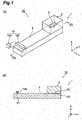
- FIG. 1 is a schematic view illustrating a configuration of a spin device according to an embodiment.
- (A) in FIG. 1 is a perspective view and (B) in FIG. 1 is a side sectional view.
- the spin device is a nanoscale device that reverses a magnetic moment using a spin current.
- a spin device that reverses the magnetic moment by application of a so-called spin Seebeck effect will be described.
- the spin Seebeck effect is a phenomenon in which the spin current is generated when a temperature difference is given to a magnetic body.
- the spin device 10 includes a spin control mechanism 1.
- the spin control mechanism 1 includes a spin portion 2 and a first channel portion 4.
- the spin portion 2 has a magnetic moment 3 that can be reversed and rotated. That is, the spin portion 2 is configured from a magnetic body.
- the spin portion 2 is configured from a ferromagnetic body, for example.
- the spin device 10 has a configuration in which a detection signal is changed according to a magnetizing direction of the magnetic moment 3 of the spin portion 2. That is, the spin device 10 has a configuration that can detect a signal that distinguishes at least a first state (for example, an ON state) and a second state (for example, an OFF state) according to the magnetizing direction of the spin portion 2.
- the spin portion 2 is in direct contact with the first channel portion 4 without intervening other members.
- the spin portion 2 and the first channel portion 4 are in contact, so that a contact surface S1 is formed.
- the size of the contact surface S1 is not limited, and the spin portion 2 and the first channel portion 4 may be in contact at one point, for example.
- the point included in the contact surface S1 is referred to as contact position P2.
- the first channel portion 4 is an insulator configured from a ferromagnetic body.
- the first channel portion 4 is a linear member having a longitudinal direction.
- the first channel portion 4 is arranged such that the longitudinal direction extends along an x direction.
- the spin portion 2 is arranged on one end portion of the first channel portion 4.
- a temperature gradient is given to the first channel portion 4.
- the temperature gradient means existence of a temperature difference according to a position.
- heat generating source 15 is thermally connected to the other end portion (a predetermined position PI) of the first channel portion 4.
- the predetermined position P1 is a position to which the heat generating source 15 is thermally connected.
- the predetermined position P1 exists on the first channel portion 4, and is separated from the contact position P2.
- the thermally connection means a state where heat can be conducted between two substances. Accordingly, the heat is conducted from the heat generating source 15 to the first channel portion 4, and a temperature gradient is provided.
- the heat generating source 15 may be a member that generates heat by Joule heat, a member that generates heat by other factors, or a member itself to which the heat has already been conducted.
- the heat generating source 15 may be a heatsink that is connected to another electronic device, and radiates heat of the electronic device.
- a power supply 15a and a resistance member 15b are employed as the heat generating source 15.
- the power supply 15a is configured to apply a voltage to the resistance member 15b.
- the power supply 15a is connected to a control unit, and may be configured to be able to turn ON/OFF the voltage application. When the voltage is applied to the resistance member 15b, the resistance member 15b generates the Joule heat.
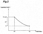
- FIG. 2 is a graph illustrating a relationship between the position of the first channel portion 4 and the temperature.
- the temperature in the predetermined position P1 increases by ⁇ T, as illustrated in FIG. 2 . That is, the temperature of the predetermined position P1 becomes T1 + ⁇ T, where the temperature of the contact position P2 is T1. Accordingly, a temperature difference ⁇ T is caused between the predetermined position P1 and the contact position P2, and the temperature gradient is caused between the predetermined position P1 and the contact position P2.
- This temperature gradient is a temperature gradient in which the temperature is decreased from the predetermined position P1 toward the contact position P2. That is, the predetermined position P1 is connected with the heat generating source 15, so that the temperature gradient is caused between the predetermined position P1 and the contact position P2.
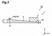
- a gradient of a thickness of the first channel portion 4 may be formed such that the thickness becomes thinner as the first channel portion 4 goes from the predetermined position P1 toward the contact position P2.
- FIG. 3 is a diagram for describing an example of the thickness of the first channel portion 4. As illustrated in FIG. 3 , a thickness t1 of the first channel portion 4 in the predetermined position P1 to which the heat generating source 15 is connected may be thicker than a thickness t2 of the contact position P2 being in contact with the spin portion 2. Then, the thickness of the first channel portion 4 may be gradually thinner toward the contact position P2 being in contact with the spin portion 2. With the configuration, heat capacity of each position is changed from the predetermined position P1 toward the contact position P2.
- the temperature gradient can be efficiently formed from the predetermined position P1 to the contact position P2 of the first channel portion 4. Accordingly, making the temperature of the predetermined position P1 higher than the temperature of the contact position P2 can be easily realized, for example. Therefore, the magnetic moment 3 of the spin portion 2 can be efficiently controlled.
- the heat is supplied from the heat generating source 15 to the predetermined position P1 of the first channel portion 4. Accordingly, the temperature gradient is generated between the predetermined position P1 and the contact position P2. Since the first channel portion 4 is configured from a ferromagnetic insulator, the spin is excited in the ferromagnetic insulator and a spin current is generated by the spin Seebeck effect. The spin current flows from the predetermined position P1 toward the contact position P2 having a lower temperature than the predetermined position P1. This spin current acts on the magnetic moment 3 of the spin portion 2 as spin-transfer torque. Accordingly, the direction of the magnetic moment 3 of the spin portion 2 is controlled.
- the magnetic moment 3 of the spin portion 2 can be controlled using the heat. Therefore, the mechanism that adjusts the temperature of electronic components can be used for downsizing and power saving. For example, by use of the heat generated from another electronic component as heat generating source 15, the mechanism that adjusts the temperature of electronic components can be further downsized or energy-saved.
- the first channel portion 4 may be formed such that the thickness becomes thinner from the predetermined position P1 toward the contact position P2.
- the temperature gradient can be efficiently formed from the predetermined position P1 to the contact position P2 of the first channel portion. Therefore, the magnetic moment 3 of the spin portion 2 can be efficiently controlled.
- a spin device 10 according to a second embodiment includes a spin control mechanism 1 similar to the spin device according to the first embodiment.
- the spin device 10 of the second embodiment is different from the spin device of the first embodiment in that the spin device 10 of the second embodiment is a spin motor by application of a so-called spin valve structure. Therefore, points overlapping with the description of the first embodiment are omitted, and the different point will be mainly described.
- FIG. 4 is a perspective view of the spin device 10 according to an embodiment.
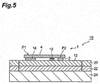
- FIG. 5 is a sectional view along line II-II of FIG. 4 .
- FIG. 6 is an enlarged view of the spin device 10 according to an embodiment.
- FIG. 7 is a schematic view for describing an operation principle of the spin device 10.
- the spin device 10 includes, for example, a second channel portion 12, a spin injector 14, a spin rotation control portion 19, and a spin portion 2.
- a spin injector 14 made of a ferromagnetic body and a spin portion 2 made of a ferromagnetic body are bridged by a second channel portion 12 made of a nonmagnetic body.
- the spin injector 14 and the spin portion 2 can be formed of a Fe, NiFe, and the like.
- the second channel portion 12 can be formed of a semiconductor material of Si or gallium arsenide (GaAs), or a nonmagnetic metal such as Ag or Cu.
- GaAs gallium arsenide
- the second channel portion 12 is arranged on a substrate 24.
- a semiconductor substrate is used, for example.
- the second channel portion 12 is a linear member, and is arranged such that its axial line direction faces an in-plane direction of the substrate 24.
- the second channel portion 12 is formed by processing a semiconductor layer 20 layered on the substrate 24 in a mesa manner.
- a line width of the second channel portion 12 is 10 ⁇ m or less, for example.
- the second channel portion 12 may be formed by processing the two-dimensional electronic gas layer 22 and the semiconductor layer 20 in a mesa manner.
- the two-dimensional electronic gas layer 22 is formed between the semiconductor layer 20 and the substrate 24.
- the spin injector 14 is provided on the substrate 24.
- the spin injector 14 is a linear member, is arranged such that its axial line direction faces the in-plane direction of the substrate 24, and is magnetized in the in-plane direction.
- the spin injector 14 is arranged on the second channel portion 12.
- the spin injector 14 is arranged to intersect with the second channel portion 12. Therefore, the spin injector 14 and the second channel portion 12 are in contact with each other (directly joined).
- An area where the spin injector 14 and the second channel portion 12 intersect with each other is a spin injection area (spin injection position).
- a line width of the spin injector 14 is 10 ⁇ m or less, for example.
- the spin portion 2 is provided on the substrate 24 being separated from the spin injector 14.
- the spin portion 2 is a disk member, and is formed such that a magnetic moment faces an in-substrate direction.
- the disk member means a member having a shape with a horizontal section that does not include an acute-angle portion.
- the disk member includes not only a plate member with a circular horizontal section, but also a member with an elliptical horizontal section, a member with a polygonal horizontal section, in which angles are large close to 180 degrees, a dot-shaped member, and a conical member.
- the spin portion 2 is arranged on the second channel portion 12.
- the spin portion 2 is in contact with (directly joined with) the second channel portion 12.
- the diameter of the spin portion 2 is 10 ⁇ m or less, for example.
- the spin portion 2 is formed such that the diameter becomes smaller than the line width of the second channel portion 12.
- the spin device 10 is an in-plane spin valve structure in which the second channel portion 12 is arranged between the spin injector 14 and the spin portion 2.
- a terminal portion 14a for current or voltage application is formed in one end portion of the spin injector 14, and a terminal portion 12a for current or voltage application is formed in one end portion (an end portion closer to the spin injector 14, of both end portions) of the second channel portion 12.
- the spin rotation control portion 19 includes a voltage control unit and a voltage application terminal (not illustrated).
- the spin rotation control portion 19 is connected to the second channel portion 12.
- the spin rotation control portion 19 is directly joined with an area on the second channel portion 12, and is an area positioned between the spin injector 14 and the spin portion 2.
- the spin rotation control portion 19 is configured to be able to apply an electric field or a magnetic field to the second channel portion 12 in order to control a rotating direction of the spin of the second channel portion 12.
- the spin rotation control portion 19 exhibits an approximately rectangular parallelepiped, and a width in a direction perpendicular to a longitudinal direction of the second channel portion 12 is 10 ⁇ m or less, for example. Note that, here, the spin portion 2 is formed such that the width in the direction perpendicular to the longitudinal direction of the second channel portion 12 becomes the line width of the second channel portion 12 or less.
- the spin device 10 includes the spin control mechanism 1.
- the spin control mechanism 1 is similar to that of the first embodiment, and includes the spin portion 2 and the first channel portion 4.
- the first channel portion 4 may extend in approximately parallel to the second channel portion 12, for example. Further, the other end portion of the first channel portion 4 may be arranged on the spin injector 14. Note that, in this case, a heat insulating material may be provided between the first channel portion 4 and the spin injector 14.
- Other configurations and modifications of the first channel portion 4 are similar to those of the first embodiment, and thus description is omitted.
- FIG. 6 is a diagram illustrating the spin device 10 that functions as a spin motor.
- the spin device 10 includes a motor rotor 30.
- the motor rotor 30 is formed of a ferromagnetic material, and is arranged above the spin portion 2, being separated from and facing the spin portion 2.
- the motor rotor 30 may just be arranged within a range where a leaked magnetic field of the spin portion 2 is transmitted, and is arranged in a range of several tens nm or less from the spin portion 2, for example. That is, the motor rotor 30 is arranged in a position where the motor rotor 30 is rotatable following the magnetic moment of the spin portion 2.
- the motor rotor 30 exhibits an approximately disk shape, and is arranged such that a rotation axis thereof becomes perpendicular to the substrate 24.
- the shape of the motor rotor 30 is not limited to the approximately disk shape, and may be, for example, a rod-like member.
- a rod-like member or the like that transmits rotary movement of the motor rotor 30 is connected to the motor rotor 30.
- a diameter of the motor rotor 30 is 10 ⁇ m or less, for example.
- the magnetic moment of the spin portion 2 is controlled by a spin current R1 flowing in the first channel portion 4 and a spin current R2 flowing in the second channel portion 12.
- the spin current R2 flowing in the second channel portion 12 mainly controls the magnetic moment of the spin portion 2
- the spin current R1 flowing in the first channel portion 4 assists easier control of the magnetic moment of the spin portion 2 by the spin current R2. That is, the spin control mechanism 1 functions as an assist mechanism of magnetization reversal of an in-plane spin valve element.
- FIG. 7 is a schematic view for describing the spin current R2 flowing in the second channel portion 12.
- the first channel portion 4 is omitted, in consideration of easy understanding of the description.
- a current is applied between the terminal portion 14a of the spin injector 14 and the terminal portion 12a of the second channel portion 12. Accordingly, spin that is antiparallel to the magnetizing direction of the spin injector 14 is injected into the second channel portion 12, as illustrated in FIG. 7 .
- the spin injected into the second channel portion 12 is diffused to both end portions of the second channel portion 12. At this time, spin antiparallel to the diffused spin flows from the spin portion 2 side to the spin injector 14 side.
- a spin current without accompanying electric changes is generated from the spin injector 14 side toward the spin portion 2 side.
- the spin flowing in the second channel portion 12 performs precession by spin-orbit interaction, and this spin-orbit interaction is controlled by the electric field by the voltage applied by the spin rotation control portion 19. That is, the direction of the spin flowing in the second channel portion 12 is changed by the applied voltage of the spin rotation control portion 19.
- the direction of the spin is changed to be gradually rotated in the in-substrate direction by ⁇ at a time according to time. That is, the direction of the spin of the spin current arriving at the spin portion 2 is rotated in the in-substrate direction by ⁇ at a time in time series.
- the spin of the second channel portion 12 provides spin-transfer torque to the magnetic moment of the spin portion 2. Therefore, the direction of the spin of the spin current is rotated in time series, so that the magnetic moment of the spin portion 2 is rotated. At this time, as illustrated in FIG. 6 , the motor rotor 30 is rotated following the magnetic moment of the spin portion 2. At this time, the rotation of the magnetic moment is converted into kinetic energy, so that the motor rotor 30 can be drive as a spin motor. Further, for example, in a case where a shape such as elliptical shape having a difference in length of an axis is employed as the horizontal section of the spin portion 2, the magnetic moment is more likely to face a major axis direction. Therefore, the direction of an initial magnetic moment can be controlled.
- the spin current R1 flowing in the first channel portion 4 related to the assist mechanism will be generally described.
- heat is supplied from a heat generating source 15 to a predetermined position P1 of the first channel portion 4. Accordingly, a temperature gradient is generated between the predetermined position P1 and a contact position P2.
- the first channel portion 4 is configured from a ferromagnetic insulator, and thus the spin is excited in the ferromagnetic insulator by spin Seebeck effect, and the spin current R1 is generated.
- the spin current R1 is generated from the predetermined position P1 toward the contact position P2 having a lower temperature than the predetermined position P1.
- This spin current R1 acts on the magnetic moment of the spin portion 2 as the spin-transfer torque. Accordingly, in controlling the magnetic moment of the spin portion 2 by the spin current R2, the spin current R1 also acts on the magnetic moment of the spin portion 2 as the spin-transfer torque. Accordingly, the magnetic moment of the spin portion 2 can be easily rotated by the spin current R1 of the first channel portion 4.
- the first channel portion 4 may be formed such that the thickness becomes thinner from the predetermined position P1 toward the contact position P2.
- the thickness of the first channel portion 4 in the predetermined position P1 may be thicker than the thickness of the contact position P2 being in contact with the spin portion 2. Then, the thickness of the first channel portion 4 may become gradually thinner toward the contact position P2 being in contact with the spin portion 2.
- the heat capacity of each position is changed from the predetermined position P1 toward the contact position P2. Therefore, the temperature gradient can be efficiently formed from the predetermined position P1 toward the contact position P2 of the first channel portion 4. Accordingly, for example, making the temperature of the predetermined position P1 higher than the temperature of the contact position P2 can be easily realized. Therefore, the magnetic moment 3 of the spin portion 2 can be efficiently controlled.
- the magnetic moment 3 of the spin portion 2 can be controlled using the heat. Therefore, the spin device 10 can be used for further downsizing or energy-saving of the mechanism that adjusts the temperature of electronic components. For example, by use of heat generated from another electronic component as the heat generating source 15, the mechanism that adjusts the temperature of electronic components can be further downsized or energy-saved.
- a spin device 10 according to a third embodiment includes a spin control mechanism 1 similar to the spin device according to the first embodiment.
- the spin device 10 according to the third embodiment is different from the spin devices according to the first and second embodiments in that a so-called perpendicular-to-surface spin valve structure is included. Therefore, points overlapping with the description of the first and second embodiments are omitted, and the difference point will be mainly described.
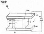
- the spin device 10 includes substrates 60 and 61, an antiferromagnetic layer 62, a pinned layer 63, an intermediate layer 64, a free layer 65, a first channel portion 4, and a potential difference generating portion 50, for example.
- the pinned layer 63, the intermediate layer 64, and the free layer 65 form a spin valve structure.
- the substrate 60 can be formed of a semiconductor material of Si or gallium arsenide (GaAs), or a nonmagnetic metal such as MgO, Ag, or Cu.
- the antiferromagnetic layer 62 made of an antiferromagnetic body is layered on the substrate 60.
- the pinned layer 63 is layered on the antiferromagnetic layer 62.
- the pinned layer 63 is made of a magnetic body.
- the direction of a magnetic moment of the pinned layer 63 is fixed to one direction by exchange coupling of the magnetic moment of the pinned layer 63 and the antiferromagnetic layer 62.
- the pinned layer 63 is formed of a ferromagnetic material.
- As the ferromagnetic material Fe, Co, Ni, or the like is used. Magnetization of the pinned layer 63 can be fixed to an arbitrary first direction.
- the first direction is, for example, a perpendicular-to-substrate direction (direction perpendicular to a substrate
- the intermediate layer 64 is provided on the pinned layer 63.
- the intermediate layer 64 may be, for example, a tunnel barrier layer for tunnel coupling of a spin valve structure.
- the intermediate layer 64 is formed of an insulator material, for example.
- As the insulator material SiO 2 , Al 2 O 3 , CoFeO, or the like is used.
- the intermediate layer 64 may be, for example, a nonmagnetic layer.
- the nonmagnetic layer is made of nonmagnetic metal of MgO, Ag, Cu, or the like.
- the free layer 65 is provided on the intermediate layer 64.
- the free layer 65 is formed of a ferromagnetic material.
- As the ferromagnetic body Fe, Co, Ni, or the like is used.
- the free layer 65 can change the direction of the magnetic moment. Magnetic anisotropy of the free layer 65 is, for example, a perpendicular-to-substrate direction (a direction perpendicular to a substrate surface). That is, the free layer 65 is configured to be able to perform magnetization reversal in the perpendicular-to-substrate direction.
- the substrate 61 that functions as a cap layer is arranged on the free layer 65.
- the substrate 61 can be formed of a semiconductor material of Si, gallium arsenide (GaAs), or the like, or a nonmagnetic metal such as MgO, Ag, or Cu. Further, an electrode may be formed in at least a part of the substrate 61. This electrode can be formed of a nonmagnetic metal of MgO, Ag, Cu, or the like.
- the spin device 10 has the pinned layer 63 and the free layer 65 layered across the intermediate layer 64 to become a layered structure that exerts tunnel magnetoresistance (TMR) or giant magnetoresistance (GMR) effect.
- the substrates 60 and 61 are provided with terminals for voltage application, respectively, and the potential difference generating portion 50 is connected to the terminals.
- the potential difference generating portion 25 provides a potential difference between the pinned layer 63 and the free layer 65.
- a resistance value between the substrates 60 and 61 is changed according to the direction of the magnetic moment of the free layer 65.
- the resistance value is changed according to the direction of the magnetic moment of the free layer 65 by the tunnel magnetoresistance (TMR) in the spin device 10.
- TMR tunnel magnetoresistance
- GMR giant magnetoresistance
- the direction of the magnetic moment of the free layer 65 can be controlled by spin excited by electrons injected into the pinned layer.
- Joule heat is generated. For example, in a case where the current flows from the substrate 60 side to the substrate 61, Joule heat is generated, and a spin current is generated in the same direction as the direction into which the current flows.
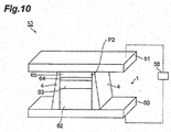
- a first channel portion 4 is arranged in contact with sides of the layered pinned layer 63, intermediate layer 64, and free layer 65.
- the spin control mechanism 1 is configured, including the free layer 65 and the first channel portion 4. This spin control mechanism 1 is the same as the spin control mechanism according to the first embodiment. Therefore, description is omitted.
- End portions of the first channel portion 4 in a vertical direction are connected to the substrate 60 and the substrate 61, respectively. Therefore, when a voltage is applied to the layered structure including the spin valve structure, Joule heat is generated in the layered structure. The generated Joule heat is conducted to the first channel portion 4 arranged at the side of the layered layer structure. At this time, the temperature of the substrate 60 side, that is, the pinned layer 63 side is higher than the temperature of the substrate 61 side, that is, the free layer 65 side. Accordingly, a temperature gradient can be caused in the first channel portion 4 from a contact position of the first channel portion 4 and the pinned layer 63 toward a contact position of the first channel portion 4 and the free layer 65.
- the spin control mechanism 1 functions as an assist mechanism, similarly to the spin control mechanism according to the second embodiment.
- the first channel portion 4 can easily control the direction of the magnetic moment of the free layer 65 using the heat generated in an electronic component.
- a gradient of the thickness of the first channel portion 4 may be formed such that the thickness becomes thinner from the pinned layer 63 side toward a contact position P2 of the first channel portion 4 and the free layer 65.
- the thickness of the first channel portion 4 at the pinned layer 63 side may be thicker than the thickness of the contact position P2 being in contact with the free layer 65.
- a point included in the contact surface where the first channel portion 4 and the free layer 65 are in contact may be employed as the contact position P2.
- the size of the contact surface is not limited, and the first channel portion 4 and the free layer 65 may be in contact at one point.
- the first channel portion 4 in which the gradient of the thickness is formed can be appropriately manufactured by a sputtering device.
- the first channel portion 4 is manufactured such that one of a film formation sample and a target is arranged in parallel to a horizontal plane, and the other is arranged inclined from the horizontal plane. In this state, sputtering is performed, so that change is given to the thickness and a film can be formed.
- the magnetic moment of the free layer 65 can be easily controlled using the heat generated by the spin valve element. Therefore, a mechanism that adjusts the temperature of electronic components, which employs the spin valve element, can be further downsized or energy-saved.
- the above-described embodiments have been described to include the case where the sizes of the configuration members of the spin device 10 are micro-order members.
- the sizes of the configuration members may be formed in the nano order, and a nanoscale spin device 10 may be formed.
- the spin injector 14 and the spin portion 2 may be arranged in any manner as long as at least a part of the spin injector 14 and the spin portion 2 is in contact with the second channel portion 12. That is, the spin injector 14 and the spin portion 2 may be arranged at a side of the second channel portion 12. Further, the spin portion 2 may have the line width of the second channel portion 12 or more.
- the spin injector 14 and the spin portion 2 may be arranged in any manner as long as at least a part of the spin injector 14 and the spin portion 2 is in contact with the first channel portion 4. That is, the spin injector 14 and the spin portion 2 may be arranged at a side of the first channel portion 4.
- the second channel portion 12 is formed of a semiconductor material. With this formation, the direction of the spin can be controlled using the circular polarization. Therefore, the number of components that are in contact with the second channel portion 12 can be decreased.
- a control unit that changes the voltage value applied to the spin injector 14 may be employed as the spin rotation control portion 19.
- a Schottky barrier is formed, and when energy of electrons and a resonance level are matched, a large current flows.
- the resonance level generated in the ferromagnetic metal/semiconductor interface can be changed. Therefore, the direction of the spin of the second channel portion 12 can be controlled with the applied voltage to the spin injector. With this formation, the number of components that are in contact with the second channel portion 12 can be decreased.
- a terminal portion 12a for current application may be formed in an end portion of the second channel portion 12 close to the spin portion 2, and a spin current accompanying the flow of electric changes may be generated by a so-called local technique, and magnetic moment of the spin portion 2 may be rotated.
- current density can be made larger than the case of the non-local technique, and thus the spin torque can be made large. Therefore, the magnetic moment of the spin portion 2 can be efficiently rotated.
- the motor rotor 30 is arranged, being separated from and facing the spin portion 2, has been described.
- the arrangement is not limited to the case where the spin portion 2 and the motor rotor 30 are separated.
- the spin portion 2 and the motor rotor 30 may be connected through a bearing or the like. Even in this case, the configuration can function as a spin motor.
- the first channel portion 4 may be separately connected to the heat generating source 15.
- the spin device 10 has industrial applicability as follows.
- the spin device 10 can be used in the field of micro electro mechanical systems (MEMS) or nano electro mechanical systems (NEMS) as a power source for motor that drives micro motor, like the spin device 10 according to the embodiments.
- MEMS micro electro mechanical systems
- NEMS nano electro mechanical systems
- the spin device 10 can be used as a device component and a motor in the electronic/electric field and in the medical field.
- the spin device 10 can be used as an electrical/electronic component in the industrial fields.
- the spin device 10 is applicable to gate control in ferromagnetic body/semiconductor hybrid structures such as memory devices or vertical nanopillars.
Landscapes
- Engineering & Computer Science (AREA)
- Computer Hardware Design (AREA)
- Microelectronics & Electronic Packaging (AREA)
- Power Engineering (AREA)
- Chemical & Material Sciences (AREA)
- Inorganic Chemistry (AREA)
- Hall/Mr Elements (AREA)
- Micromachines (AREA)
- Mram Or Spin Memory Techniques (AREA)
Abstract
Description
- The present invention relates to a spin control mechanism and a spin device.
- Heat generated from electronic components in electronic devices may be a cause that hinders normal operations of the electronic devices. Therefore, conventionally, mechanisms that adjust the temperature of electronic components are known (for example, see Patent Literature 1).
Patent Literature 1 below describes a heatsink and a fan as the mechanism that adjusts the temperature of electronic components. - Patent Literature 1: Japanese Patent Application Laid-open Publication No.
2006-107513 - Here, the inventor has calculated volumes, weights, and power consumption ratios of principal components in a lap-top computer provided with the mechanism that adjusts the temperature of electronic components. A memory device used in this computer is DRAM. As illustrated in
FIG. 11 , in the lap-top computer, the weight of the fan and the heatsink occupies about 20% of the weight of the entire computer, and the power consumption of the fan occupies about 10% of the power consumption of the entire computer. - As described above, the existence of the mechanism that adjusts the temperature of electronic components has a substantial influence on downsizing or energy saving of the computers. Therefore, employment of a spin electronic element having a smaller size and a smaller calorific value than the DRAM can be considered to suppress the volume, the weight, and the power consumption of the mechanism that adjusts the temperature of electronic components. However, the above measurement can make heat discharge capability of the mechanism that adjusts the temperature of electronic components small only by the amount of the weight or the calorific value that is smaller than the DRAM. In the field of the present technology, a new device that enables further downsizing or energy saving of the mechanism that adjusts the temperature of electronic components is desired.
- The inventor has considered that the heat generated in the electronic components can be used for the operations of the electronic components if he/she can invent a device that is operated using heat. That is, the inventor has considered that heat to be exhausted itself can be decreased by inventing the device operable by heat, and as a result, the mechanism that adjusts the temperature of electronic components can be downsized or energy-saved, and the inventor has arrived at the present invention.
- A spin control mechanism according to one aspect of the present invention includes a spin portion and a first channel portion. The spin portion has a magnetic moment. The first channel portion is provided in contact with the spin portion, and is configured from a ferromagnetic insulator. The spin control mechanism then controls a direction of the magnetic moment of the spin portion using a spin current generated by a temperature gradient provided to the first channel portion.
- In this spin control mechanism, the temperature gradient is provided to the first channel portion. When the temperature gradient exists in the ferromagnetic insulator, spin is excited in the ferromagnetic insulator by the spin Seebeck effect and a spin current is generated. That is, the spin current is generated toward the spin portion by the temperature gradient of the first channel portion, so that the magnetic moment of the spin portion can be controlled. Therefore, for example, by use of heat generated in other electronic components as a heat generating source, the mechanism that adjusts the temperature of other electronic components can be further downsized or energy-saved.
- In the spin control mechanism according to an embodiment, the temperature gradient in which a temperature becomes lower toward a contact position of the first channel portion and the spin portion may be provided to the first channel portion. With such a temperature gradient, the spin current is generated in the first channel portion toward the spin portion. Therefore, the generated spin current can change the direction of the magnetic moment of the spin portion.
- In the spin control mechanism according to an embodiment, a gradient of a thickness may be formed in the first channel portion such that the thickness becomes thinner from a predetermined position of the first channel portion toward the contact position of the first channel portion and the spin portion. With the configuration, the temperature gradient can be efficiently formed from the predetermined position of the first channel portion toward the contact position. Therefore, the magnetic moment of the spin portion can be efficiently controlled.
- In the spin control mechanism according to an embodiment, a predetermined position of the first channel portion and a heat generating source may be thermally connected in order to provide the temperature gradient between the predetermined position of the first channel portion and a contact position where the first channel portion and the spin portion are in contact with each other. With the configuration, the heat is conducted from the heat generating source to the predetermined position of the first channel portion, and the temperature gradient is generated between the predetermined position of the first channel portion configured from the ferromagnetic insulator and the contact position of the first channel portion with the spin portion.
- In the spin control mechanism according to an embodiment, the heat generating source may generate Joule heat. In an embodiment, the heat generating source may be a heatsink connected to another electronic device. In this case, by use of heat generated in other electronic components, the mechanism that adjusts the temperature of other electronic components can be further downsized or energy-saved.
- A spin device according to one aspect of the present invention is a spin device operated by a spin current. The spin device includes a spin portion, a spin injector, a first channel portion, and a second channel portion. The spin portion has a magnetic moment. The spin injector is provided separated from the spin portion, and is made of a magnetic body. The first channel portion is provided in contact with the spin portion, and is configured from a ferromagnetic insulator. The second channel portion is arranged between the spin injector and the spin portion, and is made of a nonmagnetic body joined with the spin injector and the spin portion directly or through an insulating layer. The spin device then controls a direction of the magnetic moment of the spin portion using at least one of a spin current generated in the first channel portion by a temperature gradient provided to the first channel portion, and a spin current generated in the second channel portion by application of a current or a voltage to the spin injector and the second channel portion.
- In the spin device, for example, when a current or a voltage is applied to the spin injector made of a ferromagnetic body and the second channel portion made of a nonmagnetic body, a spin current is generated in the second channel portion toward the spin portion made of a ferromagnetic body. The spin flowing in the second channel portion acts on the magnetic moment of the spin portion as spin-transfer torque. Here, a spin current is generated in the first channel portion by the spin Seebeck effect by the temperature gradient provided to the first channel portion. The spin current acts on the magnetic moment of the spin portion as the spin-transfer torque. Accordingly, the magnetic moment of the spin portion can be more easily rotated by the spin current of the first channel portion. That is, a spin device that can easily rotate a magnetic moment using heat can be realized. Therefore, for example, by use of heat generated in other electronic components, the mechanism that adjusts the temperature of other electronic components can be further downsized or energy-saved.
- In the spin device according to an embodiment, the temperature gradient in which a temperature becomes lower toward a contact position of the first channel portion and the spin portion may be provided to the first channel portion. With such a temperature gradient, the spin current is generated in the first channel portion toward the spin portion. Therefore, the generated spin current can change the direction of the magnetic moment of the spin portion.
- In the spin device according to an embodiment, a gradient of a thickness may be formed in the first channel portion such that the thickness becomes thinner from a predetermined position of the first channel portion toward a contact position of the first channel portion and the spin portion. With the configuration, the temperature gradient can be efficiently formed from the predetermined position of the first channel portion toward the contact position. Therefore, the magnetic moment of the spin portion can be efficiently controlled.
- In a spin device according to an embodiment, a predetermined position of the first channel portion and a heat generating source may be thermally connected to provide a temperature gradient between the predetermined position of the first channel portion and a contact position where the first channel portion and the spin portion are in contact with each other. With the configuration, heat is conducted from the heat generating source to the predetermined position of the first channel portion, and the temperature gradient is generated from the predetermined position of the first channel portion configured from a ferromagnetic insulator and the contact position in the first channel portion with the spin portion.
- In the spin device according to an embodiment, the heat generating source may generate heat by Joule heat. In an embodiment, the heat generating source may be a heatsink connected to another electronic device. In this case, by use of heat generated in other electronic components, the mechanism that adjusts the temperature of other electronic components can be further downsized or energy-saved.
- The spin device according to an embodiment further includes: a substrate; wherein the spin portion is a disk-like member made of a ferromagnetic body provided on the substrate, and the spin injector may be provided on the substrate, being separated from the spin portion, and may be made of a ferromagnetic body magnetized in an in-substrate direction.
- With the configuration, in a case where the spin portion is a disk-like shape, magnetic anisotropy of the spin portion in the in-substrate direction can be made uniform. Therefore, the magnetic moment of the spin portion in the in-substrate direction can be easily controlled.
- A spin device according to another aspect of the present invention includes a spin valve structure. The spin valve structure includes a pinned layer, a free layer, and an intermediate layer. In the pinned layer, a direction of a magnetic moment is fixed. The free layer is arranged facing the pinned layer, and can change the direction of a magnetic moment. The intermediate layer is arranged between the pinned layer and the free layer, and is made of a tunnel barrier layer or a nonmagnetic layer. Then, the spin device includes a potential difference generating portion and a first channel portion. The potential difference generating portion provides a potential difference between the pinned layer and the free layer. The first channel portion is made of a ferromagnetic body insulator, and is arranged in contact with sides of the pinned layer, the intermediate layer, and the free layer.
- The spin valve structure provides the potential difference to the intermediate layer sandwiched by the pinned layer and the free layer, by the potential difference generating portion, thereby to function as a switch element or a memory element having a different detection signal according to the direction of the magnetic moment of the free layer. Here, the intermediate layer is made of a tunnel barrier layer or a nonmagnetic layer. Further, when a voltage is applied by the potential difference generating portion, Joule heat is generated, and a temperature difference is caused between the pinned layer and the free layer. With this temperature difference, the temperature gradient is caused in the first channel portion being in contact with the pinned layer and the free layer. With the temperature gradient, a spin current is generated in the first channel portion. This spin current acts on the magnetic moment of the free layer as spin-transfer torque. Therefore, the magnetic moment of the free layer can be controlled by the spin current of the first channel portion. That is, by use of heat generated by a voltage for signal detection, a spin device that can easily rotate a magnetic moment of a free layer can be realized. As described above, the first channel portion can use the heat generated in the electronic component, and thus the mechanism that adjusts the temperature of electronic components can be further downsized or energy-saved.
- In the spin control mechanism according to an embodiment, a temperature gradient in which a temperature becomes lower toward a contact position of the first channel portion and the free layer may be provided to the first channel portion. With such a temperature gradient, a spin current is generated in the first channel portion toward the free layer. Therefore, the generated spin current can change the direction of the magnetic moment of the free layer.
- In the spin device according to an embodiment, a gradient of a thickness may be formed in the first channel portion such that the thickness becomes thinner from the side of the pinned layer toward the contact position of the first channel portion and the free layer. With the configuration, the temperature gradient can be efficiently formed from the predetermined position toward the contact position of the first channel portion. Therefore, the magnetic moment of the spin portion can be efficiently controlled.
- In the spin device according to an embodiment, the potential difference generating portion may generate Joule heat in the spin valve structure, and the first channel portion may be provided with a temperature gradient from the side of the pinned layer toward a contact position of the first channel portion and the free layer by the Joule heat generated in the spin valve structure.
- As described above, according to the various aspects of the present invention and various embodiments, a spin control mechanism and a spin device that control spin using heat are provided.
-
-
FIG. 1 is a schematic view illustrating a configuration of a spin device according to a first embodiment. -
FIG. 2 is a graph for describing a temperature gradient. -
FIG. 3 is a diagram for describing a thickness of a first channel portion. -
FIG. 4 is a perspective view of a spin device according to a second embodiment. -
FIG. 5 is a sectional view along line II-II ofFIG. 4 . -
FIG. 6 is an enlarged view of the spin device according to the second embodiment. -
FIG. 7 is a schematic view for describing an operation principle of a spin device. -
FIG. 8 is an enlarged view illustrating a modification of the spin device according to the second embodiment. -
FIG. 9 is a perspective view of a spin device according to a third embodiment. -
FIG. 10 is a perspective view illustrating a modification of the spin device according to the third embodiment. -
FIG. 11 is a diagram illustrating volume ratios, weight ratios, and power consumption ratios of a fan and a heatsink in a lap-top computer. - Hereinafter, embodiments will be specifically described with reference to the appended drawings. Note that, in the description of drawings, the same element is denoted with the same reference sign, and overlapping description is omitted. Further, dimension ratios of the drawings do not necessarily accord with the description.
- A spin device according to the present embodiment will be described with reference to
FIG. 1. FIG. 1 is a schematic view illustrating a configuration of a spin device according to an embodiment. (A) inFIG. 1 is a perspective view and (B) inFIG. 1 is a side sectional view. - The spin device is a nanoscale device that reverses a magnetic moment using a spin current. Here, as an example of the spin device, a spin device that reverses the magnetic moment by application of a so-called spin Seebeck effect will be described. The spin Seebeck effect is a phenomenon in which the spin current is generated when a temperature difference is given to a magnetic body.
- As illustrated in
FIG. 1 , thespin device 10 includes aspin control mechanism 1. Thespin control mechanism 1 includes aspin portion 2 and afirst channel portion 4. - The
spin portion 2 has amagnetic moment 3 that can be reversed and rotated. That is, thespin portion 2 is configured from a magnetic body. Thespin portion 2 is configured from a ferromagnetic body, for example. Here, thespin device 10 has a configuration in which a detection signal is changed according to a magnetizing direction of themagnetic moment 3 of thespin portion 2. That is, thespin device 10 has a configuration that can detect a signal that distinguishes at least a first state (for example, an ON state) and a second state (for example, an OFF state) according to the magnetizing direction of thespin portion 2. - The
spin portion 2 is in direct contact with thefirst channel portion 4 without intervening other members. Thespin portion 2 and thefirst channel portion 4 are in contact, so that a contact surface S1 is formed. Note that the size of the contact surface S1 is not limited, and thespin portion 2 and thefirst channel portion 4 may be in contact at one point, for example. Hereinafter, the point included in the contact surface S1 is referred to as contact position P2. - The
first channel portion 4 is an insulator configured from a ferromagnetic body. Thefirst channel portion 4 is a linear member having a longitudinal direction. Thefirst channel portion 4 is arranged such that the longitudinal direction extends along an x direction. Thespin portion 2 is arranged on one end portion of thefirst channel portion 4. - A temperature gradient is given to the
first channel portion 4. The temperature gradient means existence of a temperature difference according to a position. For example,heat generating source 15 is thermally connected to the other end portion (a predetermined position PI) of thefirst channel portion 4. The predetermined position P1 is a position to which theheat generating source 15 is thermally connected. The predetermined position P1 exists on thefirst channel portion 4, and is separated from the contact position P2. The thermally connection means a state where heat can be conducted between two substances. Accordingly, the heat is conducted from theheat generating source 15 to thefirst channel portion 4, and a temperature gradient is provided. - The
heat generating source 15 may be a member that generates heat by Joule heat, a member that generates heat by other factors, or a member itself to which the heat has already been conducted. Theheat generating source 15 may be a heatsink that is connected to another electronic device, and radiates heat of the electronic device. In the present embodiment, as theheat generating source 15, apower supply 15a and aresistance member 15b are employed. Thepower supply 15a is configured to apply a voltage to theresistance member 15b. Thepower supply 15a is connected to a control unit, and may be configured to be able to turn ON/OFF the voltage application. When the voltage is applied to theresistance member 15b, theresistance member 15b generates the Joule heat. The generated heat increases the temperature of thefirst channel portion 4 in the predetermined position P1.FIG. 2 is a graph illustrating a relationship between the position of thefirst channel portion 4 and the temperature. When the heat is provided from theheat generating source 15 to the predetermined position P1, the temperature in the predetermined position P1 increases by ΔT, as illustrated inFIG. 2 . That is, the temperature of the predetermined position P1 becomes T1 + ΔT, where the temperature of the contact position P2 is T1. Accordingly, a temperature difference ΔT is caused between the predetermined position P1 and the contact position P2, and the temperature gradient is caused between the predetermined position P1 and the contact position P2. This temperature gradient is a temperature gradient in which the temperature is decreased from the predetermined position P1 toward the contact position P2. That is, the predetermined position P1 is connected with theheat generating source 15, so that the temperature gradient is caused between the predetermined position P1 and the contact position P2. - In one embodiment, a gradient of a thickness of the
first channel portion 4 may be formed such that the thickness becomes thinner as thefirst channel portion 4 goes from the predetermined position P1 toward the contact position P2.FIG. 3 is a diagram for describing an example of the thickness of thefirst channel portion 4. As illustrated inFIG. 3 , a thickness t1 of thefirst channel portion 4 in the predetermined position P1 to which theheat generating source 15 is connected may be thicker than a thickness t2 of the contact position P2 being in contact with thespin portion 2. Then, the thickness of thefirst channel portion 4 may be gradually thinner toward the contact position P2 being in contact with thespin portion 2. With the configuration, heat capacity of each position is changed from the predetermined position P1 toward the contact position P2. Therefore, the temperature gradient can be efficiently formed from the predetermined position P1 to the contact position P2 of thefirst channel portion 4. Accordingly, making the temperature of the predetermined position P1 higher than the temperature of the contact position P2 can be easily realized, for example. Therefore, themagnetic moment 3 of thespin portion 2 can be efficiently controlled. - Next, an operation of the
spin device 10 will be described. First, in a case of controlling the direction of themagnetic moment 3 of thespin portion 2, the heat is supplied from theheat generating source 15 to the predetermined position P1 of thefirst channel portion 4. Accordingly, the temperature gradient is generated between the predetermined position P1 and the contact position P2. Since thefirst channel portion 4 is configured from a ferromagnetic insulator, the spin is excited in the ferromagnetic insulator and a spin current is generated by the spin Seebeck effect. The spin current flows from the predetermined position P1 toward the contact position P2 having a lower temperature than the predetermined position P1. This spin current acts on themagnetic moment 3 of thespin portion 2 as spin-transfer torque. Accordingly, the direction of themagnetic moment 3 of thespin portion 2 is controlled. - As described above, according to the
spin control mechanism 1 according to the first embodiment, themagnetic moment 3 of thespin portion 2 can be controlled using the heat. Therefore, the mechanism that adjusts the temperature of electronic components can be used for downsizing and power saving. For example, by use of the heat generated from another electronic component asheat generating source 15, the mechanism that adjusts the temperature of electronic components can be further downsized or energy-saved. - Further, according to the
spin control mechanism 1 according to the first embodiment, thefirst channel portion 4 may be formed such that the thickness becomes thinner from the predetermined position P1 toward the contact position P2. With the configuration, the temperature gradient can be efficiently formed from the predetermined position P1 to the contact position P2 of the first channel portion. Therefore, themagnetic moment 3 of thespin portion 2 can be efficiently controlled. - A
spin device 10 according to a second embodiment includes aspin control mechanism 1 similar to the spin device according to the first embodiment. Thespin device 10 of the second embodiment is different from the spin device of the first embodiment in that thespin device 10 of the second embodiment is a spin motor by application of a so-called spin valve structure. Therefore, points overlapping with the description of the first embodiment are omitted, and the different point will be mainly described. - The
spin device 10 according to the present embodiment will be described with reference toFIGS. 4 to 7 .FIG. 4 is a perspective view of thespin device 10 according to an embodiment.FIG. 5 is a sectional view along line II-II ofFIG. 4 .FIG. 6 is an enlarged view of thespin device 10 according to an embodiment.FIG. 7 is a schematic view for describing an operation principle of thespin device 10. - As illustrated in
FIG. 4 , thespin device 10 includes, for example, asecond channel portion 12, aspin injector 14, a spinrotation control portion 19, and aspin portion 2. Here, an in-plane spin valve structure is formed in which aspin injector 14 made of a ferromagnetic body and aspin portion 2 made of a ferromagnetic body are bridged by asecond channel portion 12 made of a nonmagnetic body. Thespin injector 14 and thespin portion 2 can be formed of a Fe, NiFe, and the like. Thesecond channel portion 12 can be formed of a semiconductor material of Si or gallium arsenide (GaAs), or a nonmagnetic metal such as Ag or Cu. Hereinafter, a case in which thesecond channel portion 12 is formed of the semiconductor material will be described. - As illustrated in
FIGS. 4 and5 , thesecond channel portion 12 is arranged on asubstrate 24. As thesubstrate 24, a semiconductor substrate is used, for example. Thesecond channel portion 12 is a linear member, and is arranged such that its axial line direction faces an in-plane direction of thesubstrate 24. Thesecond channel portion 12 is formed by processing asemiconductor layer 20 layered on thesubstrate 24 in a mesa manner. A line width of thesecond channel portion 12 is 10 µm or less, for example. In a case where a two-dimensionalelectronic gas layer 22 is formed between thesubstrate 24 and thesemiconductor layer 20, thesecond channel portion 12 may be formed by processing the two-dimensionalelectronic gas layer 22 and thesemiconductor layer 20 in a mesa manner. For example, in a case where a GaAs substrate is used as thesubstrate 24, and thesemiconductor layer 20 is formed by doping thesubstrate 24 with electrons, the two-dimensionalelectronic gas layer 22 is formed between thesemiconductor layer 20 and thesubstrate 24. - The
spin injector 14 is provided on thesubstrate 24. Thespin injector 14 is a linear member, is arranged such that its axial line direction faces the in-plane direction of thesubstrate 24, and is magnetized in the in-plane direction. Note that, here thespin injector 14 is arranged on thesecond channel portion 12. Thespin injector 14 is arranged to intersect with thesecond channel portion 12. Therefore, thespin injector 14 and thesecond channel portion 12 are in contact with each other (directly joined). An area where thespin injector 14 and thesecond channel portion 12 intersect with each other is a spin injection area (spin injection position). A line width of thespin injector 14 is 10 µm or less, for example. - The
spin portion 2 is provided on thesubstrate 24 being separated from thespin injector 14. Thespin portion 2 is a disk member, and is formed such that a magnetic moment faces an in-substrate direction. Note that the disk member means a member having a shape with a horizontal section that does not include an acute-angle portion. The disk member includes not only a plate member with a circular horizontal section, but also a member with an elliptical horizontal section, a member with a polygonal horizontal section, in which angles are large close to 180 degrees, a dot-shaped member, and a conical member. Here, thespin portion 2 is arranged on thesecond channel portion 12. Thespin portion 2 is in contact with (directly joined with) thesecond channel portion 12. The diameter of thespin portion 2 is 10 µm or less, for example. Here, thespin portion 2 is formed such that the diameter becomes smaller than the line width of thesecond channel portion 12. - As described above, the
spin device 10 is an in-plane spin valve structure in which thesecond channel portion 12 is arranged between thespin injector 14 and thespin portion 2. Aterminal portion 14a for current or voltage application is formed in one end portion of thespin injector 14, and aterminal portion 12a for current or voltage application is formed in one end portion (an end portion closer to thespin injector 14, of both end portions) of thesecond channel portion 12. - The spin
rotation control portion 19 includes a voltage control unit and a voltage application terminal (not illustrated). The spinrotation control portion 19 is connected to thesecond channel portion 12. For example, the spinrotation control portion 19 is directly joined with an area on thesecond channel portion 12, and is an area positioned between thespin injector 14 and thespin portion 2. The spinrotation control portion 19 is configured to be able to apply an electric field or a magnetic field to thesecond channel portion 12 in order to control a rotating direction of the spin of thesecond channel portion 12. The spinrotation control portion 19 exhibits an approximately rectangular parallelepiped, and a width in a direction perpendicular to a longitudinal direction of thesecond channel portion 12 is 10 µm or less, for example. Note that, here, thespin portion 2 is formed such that the width in the direction perpendicular to the longitudinal direction of thesecond channel portion 12 becomes the line width of thesecond channel portion 12 or less. - Here, the
spin device 10 includes thespin control mechanism 1. Thespin control mechanism 1 is similar to that of the first embodiment, and includes thespin portion 2 and thefirst channel portion 4. Thefirst channel portion 4 may extend in approximately parallel to thesecond channel portion 12, for example. Further, the other end portion of thefirst channel portion 4 may be arranged on thespin injector 14. Note that, in this case, a heat insulating material may be provided between thefirst channel portion 4 and thespin injector 14. Other configurations and modifications of thefirst channel portion 4 are similar to those of the first embodiment, and thus description is omitted. -
FIG. 6 is a diagram illustrating thespin device 10 that functions as a spin motor. As illustrated inFIG. 6 , thespin device 10 includes amotor rotor 30. Themotor rotor 30 is formed of a ferromagnetic material, and is arranged above thespin portion 2, being separated from and facing thespin portion 2. Themotor rotor 30 may just be arranged within a range where a leaked magnetic field of thespin portion 2 is transmitted, and is arranged in a range of several tens nm or less from thespin portion 2, for example. That is, themotor rotor 30 is arranged in a position where themotor rotor 30 is rotatable following the magnetic moment of thespin portion 2. Themotor rotor 30 exhibits an approximately disk shape, and is arranged such that a rotation axis thereof becomes perpendicular to thesubstrate 24. Note that the shape of themotor rotor 30 is not limited to the approximately disk shape, and may be, for example, a rod-like member. A rod-like member or the like that transmits rotary movement of themotor rotor 30 is connected to themotor rotor 30. A diameter of themotor rotor 30 is 10 µm or less, for example. - An operation of the
spin device 10 having the above configuration will be described. As illustrated inFIG. 6 , the magnetic moment of thespin portion 2 is controlled by a spin current R1 flowing in thefirst channel portion 4 and a spin current R2 flowing in thesecond channel portion 12. Note that the spin current R2 flowing in thesecond channel portion 12 mainly controls the magnetic moment of thespin portion 2, and the spin current R1 flowing in thefirst channel portion 4 assists easier control of the magnetic moment of thespin portion 2 by the spin current R2. That is, thespin control mechanism 1 functions as an assist mechanism of magnetization reversal of an in-plane spin valve element. - Firstly, the spin current R2 flowing in the
second channel portion 12, which is related to main control, will be generally described. -
FIG. 7 is a schematic view for describing the spin current R2 flowing in thesecond channel portion 12. InFIG. 7 , thefirst channel portion 4 is omitted, in consideration of easy understanding of the description. First, a current is applied between theterminal portion 14a of thespin injector 14 and theterminal portion 12a of thesecond channel portion 12. Accordingly, spin that is antiparallel to the magnetizing direction of thespin injector 14 is injected into thesecond channel portion 12, as illustrated inFIG. 7 . The spin injected into thesecond channel portion 12 is diffused to both end portions of thesecond channel portion 12. At this time, spin antiparallel to the diffused spin flows from thespin portion 2 side to thespin injector 14 side. Therefore, a spin current without accompanying electric changes is generated from thespin injector 14 side toward thespin portion 2 side. The spin flowing in thesecond channel portion 12 performs precession by spin-orbit interaction, and this spin-orbit interaction is controlled by the electric field by the voltage applied by the spinrotation control portion 19. That is, the direction of the spin flowing in thesecond channel portion 12 is changed by the applied voltage of the spinrotation control portion 19. Here, the direction of the spin is changed to be gradually rotated in the in-substrate direction by Δθ at a time according to time. That is, the direction of the spin of the spin current arriving at thespin portion 2 is rotated in the in-substrate direction by Δθ at a time in time series. The spin of thesecond channel portion 12 provides spin-transfer torque to the magnetic moment of thespin portion 2. Therefore, the direction of the spin of the spin current is rotated in time series, so that the magnetic moment of thespin portion 2 is rotated. At this time, as illustrated inFIG. 6 , themotor rotor 30 is rotated following the magnetic moment of thespin portion 2. At this time, the rotation of the magnetic moment is converted into kinetic energy, so that themotor rotor 30 can be drive as a spin motor. Further, for example, in a case where a shape such as elliptical shape having a difference in length of an axis is employed as the horizontal section of thespin portion 2, the magnetic moment is more likely to face a major axis direction. Therefore, the direction of an initial magnetic moment can be controlled. - Next, the spin current R1 flowing in the
first channel portion 4 related to the assist mechanism will be generally described. In a case of controlling the direction of the magnetic moment of thespin portion 2, heat is supplied from aheat generating source 15 to a predetermined position P1 of thefirst channel portion 4. Accordingly, a temperature gradient is generated between the predetermined position P1 and a contact position P2. Thefirst channel portion 4 is configured from a ferromagnetic insulator, and thus the spin is excited in the ferromagnetic insulator by spin Seebeck effect, and the spin current R1 is generated. The spin current R1 is generated from the predetermined position P1 toward the contact position P2 having a lower temperature than the predetermined position P1. This spin current R1 acts on the magnetic moment of thespin portion 2 as the spin-transfer torque. Accordingly, in controlling the magnetic moment of thespin portion 2 by the spin current R2, the spin current R1 also acts on the magnetic moment of thespin portion 2 as the spin-transfer torque. Accordingly, the magnetic moment of thespin portion 2 can be easily rotated by the spin current R1 of thefirst channel portion 4. - Further, in the present embodiment, as illustrated in
FIG. 8 , thefirst channel portion 4 may be formed such that the thickness becomes thinner from the predetermined position P1 toward the contact position P2. For example, the thickness of thefirst channel portion 4 in the predetermined position P1 may be thicker than the thickness of the contact position P2 being in contact with thespin portion 2. Then, the thickness of thefirst channel portion 4 may become gradually thinner toward the contact position P2 being in contact with thespin portion 2. With the configuration, the heat capacity of each position is changed from the predetermined position P1 toward the contact position P2. Therefore, the temperature gradient can be efficiently formed from the predetermined position P1 toward the contact position P2 of thefirst channel portion 4. Accordingly, for example, making the temperature of the predetermined position P1 higher than the temperature of the contact position P2 can be easily realized. Therefore, themagnetic moment 3 of thespin portion 2 can be efficiently controlled. - As described above, according to the
spin device 10 according of the second embodiment, themagnetic moment 3 of thespin portion 2 can be controlled using the heat. Therefore, thespin device 10 can be used for further downsizing or energy-saving of the mechanism that adjusts the temperature of electronic components. For example, by use of heat generated from another electronic component as theheat generating source 15, the mechanism that adjusts the temperature of electronic components can be further downsized or energy-saved. - A
spin device 10 according to a third embodiment includes aspin control mechanism 1 similar to the spin device according to the first embodiment. Thespin device 10 according to the third embodiment is different from the spin devices according to the first and second embodiments in that a so-called perpendicular-to-surface spin valve structure is included. Therefore, points overlapping with the description of the first and second embodiments are omitted, and the difference point will be mainly described. - As illustrated in
FIG. 9 , thespin device 10 includessubstrates antiferromagnetic layer 62, a pinnedlayer 63, anintermediate layer 64, afree layer 65, afirst channel portion 4, and a potentialdifference generating portion 50, for example. The pinnedlayer 63, theintermediate layer 64, and thefree layer 65 form a spin valve structure. - The
substrate 60 can be formed of a semiconductor material of Si or gallium arsenide (GaAs), or a nonmagnetic metal such as MgO, Ag, or Cu. Theantiferromagnetic layer 62 made of an antiferromagnetic body is layered on thesubstrate 60. The pinnedlayer 63 is layered on theantiferromagnetic layer 62. The pinnedlayer 63 is made of a magnetic body. The direction of a magnetic moment of the pinnedlayer 63 is fixed to one direction by exchange coupling of the magnetic moment of the pinnedlayer 63 and theantiferromagnetic layer 62. The pinnedlayer 63 is formed of a ferromagnetic material. As the ferromagnetic material, Fe, Co, Ni, or the like is used. Magnetization of the pinnedlayer 63 can be fixed to an arbitrary first direction. The first direction is, for example, a perpendicular-to-substrate direction (direction perpendicular to a substrate surface). - The
intermediate layer 64 is provided on the pinnedlayer 63. Theintermediate layer 64 may be, for example, a tunnel barrier layer for tunnel coupling of a spin valve structure. In this case, theintermediate layer 64 is formed of an insulator material, for example. As the insulator material, SiO2, Al2O3, CoFeO, or the like is used. Further, theintermediate layer 64 may be, for example, a nonmagnetic layer. The nonmagnetic layer is made of nonmagnetic metal of MgO, Ag, Cu, or the like. - The
free layer 65 is provided on theintermediate layer 64. Thefree layer 65 is formed of a ferromagnetic material. As the ferromagnetic body, Fe, Co, Ni, or the like is used. Thefree layer 65 can change the direction of the magnetic moment. Magnetic anisotropy of thefree layer 65 is, for example, a perpendicular-to-substrate direction (a direction perpendicular to a substrate surface). That is, thefree layer 65 is configured to be able to perform magnetization reversal in the perpendicular-to-substrate direction. Thesubstrate 61 that functions as a cap layer is arranged on thefree layer 65. Thesubstrate 61 can be formed of a semiconductor material of Si, gallium arsenide (GaAs), or the like, or a nonmagnetic metal such as MgO, Ag, or Cu. Further, an electrode may be formed in at least a part of thesubstrate 61. This electrode can be formed of a nonmagnetic metal of MgO, Ag, Cu, or the like. - As described above, the
spin device 10 has the pinnedlayer 63 and thefree layer 65 layered across theintermediate layer 64 to become a layered structure that exerts tunnel magnetoresistance (TMR) or giant magnetoresistance (GMR) effect. Thesubstrates difference generating portion 50 is connected to the terminals. The potential difference generating portion 25 provides a potential difference between the pinnedlayer 63 and thefree layer 65. A resistance value between thesubstrates free layer 65. In a case where theintermediate layer 64 is mainly configured from an insulator, the resistance value is changed according to the direction of the magnetic moment of thefree layer 65 by the tunnel magnetoresistance (TMR) in thespin device 10. Meanwhile, in a case where theintermediate layer 64 is mainly configured from a nonmagnetic body, the resistance value is changed according to the direction of the magnetic moment of thefree layer 65 by the giant magnetoresistance (GMR) in thespin device 10. The direction of the magnetic moment of thefree layer 65 can be controlled by spin excited by electrons injected into the pinned layer. Further, by application of a current to the spin valve structure, Joule heat is generated. For example, in a case where the current flows from thesubstrate 60 side to thesubstrate 61, Joule heat is generated, and a spin current is generated in the same direction as the direction into which the current flows. - Here, a
first channel portion 4 is arranged in contact with sides of the layered pinnedlayer 63,intermediate layer 64, andfree layer 65. Thespin control mechanism 1 is configured, including thefree layer 65 and thefirst channel portion 4. Thisspin control mechanism 1 is the same as the spin control mechanism according to the first embodiment. Therefore, description is omitted. - End portions of the
first channel portion 4 in a vertical direction are connected to thesubstrate 60 and thesubstrate 61, respectively. Therefore, when a voltage is applied to the layered structure including the spin valve structure, Joule heat is generated in the layered structure. The generated Joule heat is conducted to thefirst channel portion 4 arranged at the side of the layered layer structure. At this time, the temperature of thesubstrate 60 side, that is, the pinnedlayer 63 side is higher than the temperature of thesubstrate 61 side, that is, thefree layer 65 side. Accordingly, a temperature gradient can be caused in thefirst channel portion 4 from a contact position of thefirst channel portion 4 and the pinnedlayer 63 toward a contact position of thefirst channel portion 4 and thefree layer 65. Therefore, spin is excited in thefirst channel portion 4, and a spin current is generated. The spin current acts on the magnetic moment of thefree layer 65 as spin-transfer torque. At this time, the magnetic moment of thefree layer 65 can be more easily controlled by the spin current of thefirst channel portion 4. That is, thespin control mechanism 1 according to the present embodiment functions as an assist mechanism, similarly to the spin control mechanism according to the second embodiment. As described above, thefirst channel portion 4 can easily control the direction of the magnetic moment of thefree layer 65 using the heat generated in an electronic component. - Further, as illustrated in
FIG. 10 , in the present embodiment, a gradient of the thickness of thefirst channel portion 4 may be formed such that the thickness becomes thinner from the pinnedlayer 63 side toward a contact position P2 of thefirst channel portion 4 and thefree layer 65. The thickness of thefirst channel portion 4 at the pinnedlayer 63 side may be thicker than the thickness of the contact position P2 being in contact with thefree layer 65. In this case, for example, a point included in the contact surface where thefirst channel portion 4 and thefree layer 65 are in contact may be employed as the contact position P2. The size of the contact surface is not limited, and thefirst channel portion 4 and thefree layer 65 may be in contact at one point. - With the configuration, heat capacity of each position of the
first channel portion 4 is changed toward thefree layer 65. Therefore, the temperature gradient can be efficiently formed from the pinnedlayer 63 side of thefirst channel portion 4 toward the contact position. Therefore, the magnetic moment of thefree layer 65 can be efficiently controlled. - The
first channel portion 4 in which the gradient of the thickness is formed can be appropriately manufactured by a sputtering device. Thefirst channel portion 4 is manufactured such that one of a film formation sample and a target is arranged in parallel to a horizontal plane, and the other is arranged inclined from the horizontal plane. In this state, sputtering is performed, so that change is given to the thickness and a film can be formed. - As described above, according to the
spin device 10 of the third embodiment, the magnetic moment of thefree layer 65 can be easily controlled using the heat generated by the spin valve element. Therefore, a mechanism that adjusts the temperature of electronic components, which employs the spin valve element, can be further downsized or energy-saved. - The above-described embodiments can be made into various modifications.
- For example, the above-described embodiments have been described to include the case where the sizes of the configuration members of the
spin device 10 are micro-order members. However, the sizes of the configuration members may be formed in the nano order, and ananoscale spin device 10 may be formed. - Further, in the above-described second embodiment, an example in which the
spin injector 14, the spinrotation control portion 19, and thespin portion 2 are directly joined with thesecond channel portion 12 has been described. However, at least one of thespin injector 14, the spinrotation control portion 19, and thespin portion 2 may be joined with thesecond channel portion 12 through an insulating layer. Even this configuration can function as thespin device 10. - Further, in the above-described second embodiment, an example in which the
spin injector 14 and thespin portion 2 are arranged above thesecond channel portion 12 has been described. However, thespin injector 14 and thespin portion 2 may be arranged in any manner as long as at least a part of thespin injector 14 and thespin portion 2 is in contact with thesecond channel portion 12. That is, thespin injector 14 and thespin portion 2 may be arranged at a side of thesecond channel portion 12. Further, thespin portion 2 may have the line width of thesecond channel portion 12 or more. - Further, in the above-described second embodiment, an example in which the
first channel portion 4 is arranged above thespin portion 2 has been described. However, thespin injector 14 and thespin portion 2 may be arranged in any manner as long as at least a part of thespin injector 14 and thespin portion 2 is in contact with thefirst channel portion 4. That is, thespin injector 14 and thespin portion 2 may be arranged at a side of thefirst channel portion 4. - Further, in the above-described second embodiment, an example of applying a current to the
second channel portion 12 as the spinrotation control portion 19 has been described. However, another spin rotation control portion may be employed. For example, an irradiation portion that irradiates thesecond channel portion 12 with circular polarization may be employed as the spinrotation control portion 19. Note that, in this case, thesecond channel portion 12 is formed of a semiconductor material. With this formation, the direction of the spin can be controlled using the circular polarization. Therefore, the number of components that are in contact with thesecond channel portion 12 can be decreased. - Further, a control unit that changes the voltage value applied to the
spin injector 14 may be employed as the spinrotation control portion 19. In an interface between the ferromagnetic metal and the semiconductor, a Schottky barrier is formed, and when energy of electrons and a resonance level are matched, a large current flows. By change of the voltage value to be applied to thespin injector 14, the resonance level generated in the ferromagnetic metal/semiconductor interface can be changed. Therefore, the direction of the spin of thesecond channel portion 12 can be controlled with the applied voltage to the spin injector. With this formation, the number of components that are in contact with thesecond channel portion 12 can be decreased. - Further, in the above-described second embodiment, an example of generating the spin current without accompanying a flow of electric charges by a so-called non-local technique, and rotating the
spin portion 2 has been described. However, aterminal portion 12a for current application may be formed in an end portion of thesecond channel portion 12 close to thespin portion 2, and a spin current accompanying the flow of electric changes may be generated by a so-called local technique, and magnetic moment of thespin portion 2 may be rotated. In this case, current density can be made larger than the case of the non-local technique, and thus the spin torque can be made large. Therefore, the magnetic moment of thespin portion 2 can be efficiently rotated. - Further, in the above-described second embodiment, an example in which the
motor rotor 30 is arranged, being separated from and facing thespin portion 2, has been described. However, the arrangement is not limited to the case where thespin portion 2 and themotor rotor 30 are separated. For example, thespin portion 2 and themotor rotor 30 may be connected through a bearing or the like. Even in this case, the configuration can function as a spin motor. - Further, in the third embodiment, the
first channel portion 4 may be separately connected to theheat generating source 15. - The
spin device 10 has industrial applicability as follows. Thespin device 10 can be used in the field of micro electro mechanical systems (MEMS) or nano electro mechanical systems (NEMS) as a power source for motor that drives micro motor, like thespin device 10 according to the embodiments. Further, thespin device 10 can be used as a device component and a motor in the electronic/electric field and in the medical field. Further, thespin device 10 can be used as an electrical/electronic component in the industrial fields. For example, thespin device 10 is applicable to gate control in ferromagnetic body/semiconductor hybrid structures such as memory devices or vertical nanopillars. - 1... Spin control mechanism, 10... Spin device, 2 ... Spin portion, 4... First channel portion, 12 ... Second channel portion, 14... Spin injector, 15...Heat generating source, 24...Substrate, 50...Potential difference generating portion, 63...Pinned layer, 64...Intermediate layer, 65...Free layer, P1...Predetermined position, P2...Contact position.
Claims (17)
- A spin control mechanism that controls a direction of a magnetic moment, the spin control mechanism comprising:a spin portion having the magnetic moment; anda first channel portion provided in contact with the spin portion and configured from a ferromagnetic insulator,wherein the direction of the magnetic moment of the spin portion is controlled using a spin current generated by a temperature gradient provided to the first channel portion.
- The spin control mechanism according to claim 1, wherein the temperature gradient in which a temperature becomes lower toward a contact position of the first channel portion and the spin portion is provided to the first channel portion.
- The spin control mechanism according to claim 1 or 2, wherein a gradient of a thickness is formed in the first channel portion such that the thickness becomes thinner from a predetermined position of the first channel portion toward the contact position of the first channel portion and the spin portion.
- The spin control mechanism according to any one of claims 1 to 3, wherein a predetermined position of the first channel portion and a heat generating source are thermally connected in order to provide the temperature gradient between the predetermined position of the first channel portion and a contact position where the first channel portion and the spin portion are in contact with each other.
- The spin control mechanism according to claim 4, wherein the heat generating source generates Joule heat.
- The spin control mechanism according to claim 4, wherein the heat generating source is a heatsink connected to another electronic device.
- A spin device that is operated by a spin current, the spin device comprising:a spin portion having a magnetic moment;a spin injector provided separated from the spin portion, and made of a magnetic body;a first channel portion provided in contact with the spin portion, and configured from a ferromagnetic insulator; anda second channel portion arranged between the spin injector and the spin portion, and made of a nonmagnetic body joined with the spin injector and the spin portion directly or through an insulating layer,wherein a direction of the magnetic moment of the spin portion is controlled using at least one of a spin current generated in the first channel portion by a temperature gradient provided to the first channel portion, and a spin current generated in the second channel portion by application of a current or a voltage to the spin injector and the second channel portion.
- The spin device according to claim 7, wherein the temperature gradient in which a temperature becomes lower toward a contact position of the first channel portion and the spin portion is provided to the first channel portion.
- The spin device according to claim 7 or 8, wherein a gradient of a thickness is formed in the first channel portion such that the thickness becomes thinner from a predetermined position of the first channel portion toward a contact position of the first channel portion and the spin portion.
- The spin device according to any one of claims 7 to 9, wherein a predetermined position of the first channel portion and a heat generating source are thermally connected in order to provide the temperature gradient between the predetermined position and a contact position where the first channel portion and the spin portion are in contact with each other.
- The spin device according to claim 10, wherein the heat generating source generates heat by Joule heat.
- The spin device according to claim 10, wherein the heat generating source is a heatsink connected to another electronic device.
- The spin device according to any one of claims 7 to 12, further comprising:a substrate; whereinthe spin portion is a disk-like member made of a ferromagnetic body provided on the substrate, andthe spin injector is provided on the substrate, being separated from the spin portion, and is made of a ferromagnetic body magnetized in an in-substrate direction.
- A spin device having a spin valve structure including a pinned layer in which a direction of a magnetic moment is fixed, a free layer arranged facing the pinned layer and capable of changing the direction of a magnetic moment, and an intermediate layer arranged between the pinned layer and the free layer and made of a tunnel barrier layer or a nonmagnetic layer, the spin device comprising:a potential difference generating portion configured to provide a potential difference between the pinned layer and the free layer; anda first channel portion made of a ferromagnetic body insulator, and arranged in contact with sides of the pinned layer, the intermediate layer, and the free layer.
- The spin control mechanism according to claim 14, wherein a temperature gradient in which a temperature becomes lower toward a contact position of the first channel portion and the free layer is provided to the first channel portion.
- The spin device according to claim 14 or 15, wherein a gradient of a thickness is formed in the first channel portion such that the thickness becomes thinner from the side of the pinned layer toward the contact position of the first channel portion and the free layer.
- The spin device according to any one of claims 14 to 16, wherein the potential difference generating portion generates Joule heat in the spin valve structure, and
the first channel portion is provided with a temperature gradient from the side of the pinned layer toward a contact position of the first channel portion and the free layer by the Joule heat generated in the spin valve structure.
Applications Claiming Priority (2)
| Application Number | Priority Date | Filing Date | Title |
|---|---|---|---|
| JP2013227153 | 2013-10-31 | ||
| PCT/JP2014/078816 WO2015064663A1 (en) | 2013-10-31 | 2014-10-29 | Spin control mechanism and spin device |
Publications (3)
| Publication Number | Publication Date |
|---|---|
| EP3065181A1 true EP3065181A1 (en) | 2016-09-07 |
| EP3065181A4 EP3065181A4 (en) | 2017-11-08 |
| EP3065181B1 EP3065181B1 (en) | 2019-06-26 |
Family
ID=53004262
Family Applications (1)
| Application Number | Title | Priority Date | Filing Date |
|---|---|---|---|
| EP14857027.8A Not-in-force EP3065181B1 (en) | 2013-10-31 | 2014-10-29 | Spin control mechanism and spin device |
Country Status (7)
| Country | Link |
|---|---|
| US (1) | US9882118B2 (en) |
| EP (1) | EP3065181B1 (en) |
| JP (1) | JP6090878B2 (en) |
| KR (1) | KR101827294B1 (en) |
| CN (1) | CN105659386B (en) |
| TW (1) | TWI628788B (en) |
| WO (1) | WO2015064663A1 (en) |
Families Citing this family (5)
| Publication number | Priority date | Publication date | Assignee | Title |
|---|---|---|---|---|
| EP3065181B1 (en) * | 2013-10-31 | 2019-06-26 | Japan Science and Technology Agency | Spin control mechanism and spin device |
| TWI680598B (en) * | 2015-05-22 | 2019-12-21 | 國立研究開發法人科學技術振興機構 | Pulse generator |
| JP6907696B2 (en) * | 2016-07-29 | 2021-07-21 | Tdk株式会社 | Method for manufacturing spin current magnetization reversing element, element assembly and spin current magnetization reversing element |
| US9934798B1 (en) * | 2016-09-28 | 2018-04-03 | Seagate Technology Llc | Lateral spin valve reader with vertically-integrated two-dimensional semiconducting channel |
| KR102611433B1 (en) | 2018-11-14 | 2023-12-08 | 삼성전자주식회사 | Magnetic memory devices |
Family Cites Families (56)
| Publication number | Priority date | Publication date | Assignee | Title |
|---|---|---|---|---|
| TW546647B (en) * | 2001-01-19 | 2003-08-11 | Matsushita Electric Industrial Co Ltd | Magnetic storage element, the manufacturing method and driving method thereof, and memory array |
| US7516334B2 (en) | 2001-03-22 | 2009-04-07 | Sony Computer Entertainment Inc. | Power management for processing modules |
| JP4270797B2 (en) * | 2002-03-12 | 2009-06-03 | Tdk株式会社 | Magnetic detection element |
| JP3863484B2 (en) * | 2002-11-22 | 2006-12-27 | 株式会社東芝 | Magnetoresistive element and magnetic memory |
| US7675129B2 (en) * | 2002-12-13 | 2010-03-09 | Japan Science And Technology Agency | Spin injection device, magnetic device using the same, magnetic thin film used in the same |
| JP2004289100A (en) * | 2003-01-31 | 2004-10-14 | Japan Science & Technology Agency | CPP type giant magnetoresistive element, magnetic component using the same, and magnetic device |
| US7324309B1 (en) * | 2003-03-06 | 2008-01-29 | Maxtor Corporation | Cross-track shielding in a GMR head |
| JP2005109240A (en) * | 2003-09-30 | 2005-04-21 | Tdk Corp | Magnetoresistive effect element and magnetic head |
| WO2005086250A1 (en) * | 2004-03-05 | 2005-09-15 | National Institute Of Advanced Industrial Science And Technology | Tunnel junction device |
| JP4677589B2 (en) * | 2005-03-18 | 2011-04-27 | 独立行政法人科学技術振興機構 | Transmission circuit integrated microwave generation element and microwave detection method, microwave detection circuit, microwave detection element, and transmission circuit integrated microwave detection element |
| US7602591B2 (en) * | 2005-06-22 | 2009-10-13 | Tdk Corporation | Exchange-coupled free layer with out-of-plane magnetization |
| US20060291107A1 (en) * | 2005-06-22 | 2006-12-28 | Tdk Corporation | Magnetoresistive element with tilted in-stack bias |
| US7918014B2 (en) * | 2005-07-13 | 2011-04-05 | Headway Technologies, Inc. | Method of manufacturing a CPP structure with enhanced GMR ratio |
| US8018345B2 (en) * | 2005-09-08 | 2011-09-13 | Sri International | RFID tags having ferromagnetic patches |
| JP2007266498A (en) * | 2006-03-29 | 2007-10-11 | Toshiba Corp | Magnetic recording element and magnetic memory |
| JP2007273493A (en) * | 2006-03-30 | 2007-10-18 | Fujitsu Ltd | Magnetic memory device and manufacturing method thereof |
| JP2007329157A (en) * | 2006-06-06 | 2007-12-20 | Tdk Corp | Magnetoresistive element, thin film magnetic head, substrate, wafer, head gimbal assembly, hard disk device, and method of manufacturing magnetoresistive element |
| JP2008034689A (en) * | 2006-07-31 | 2008-02-14 | Tdk Corp | Magnetoresistive element, thin film magnetic head, head gimbal assembly, head arm assembly, magnetic disk drive, magnetic sensor and magnetic memory |
| JP5397902B2 (en) * | 2007-03-16 | 2014-01-22 | 国立大学法人東北大学 | Spin relaxation variation method, spin current detection method, and spintronic device using spin relaxation |
| JP2008288235A (en) * | 2007-05-15 | 2008-11-27 | Tdk Corp | Magnetic detecting element and manufacturing method thereof |
| JP5267967B2 (en) * | 2007-11-22 | 2013-08-21 | 国立大学法人東北大学 | Spin current heat conversion element and thermoelectric conversion element |
| US20100148167A1 (en) * | 2008-12-12 | 2010-06-17 | Everspin Technologies, Inc. | Magnetic tunnel junction stack |
| US7974120B2 (en) * | 2009-01-23 | 2011-07-05 | Infineon Technologies Ag | Spin device |
| KR20100104497A (en) * | 2009-03-18 | 2010-09-29 | 주식회사 하이닉스반도체 | Semiconductor memory device including a magnetic tunnel junction element, and manufacturing method thereof |
| JP4908540B2 (en) * | 2009-03-25 | 2012-04-04 | 株式会社東芝 | Spin MOSFET and reconfigurable logic circuit |
| WO2010143370A1 (en) * | 2009-06-09 | 2010-12-16 | キヤノンアネルバ株式会社 | Magnetic sensor laminated body, film forming method for same, film formation control program, and recording medium |
| JP5544547B2 (en) * | 2009-07-09 | 2014-07-09 | 国立大学法人九州大学 | Magnetization reversal device, storage element, and magnetic field generation device |
| WO2011118374A1 (en) * | 2010-03-25 | 2011-09-29 | 日本電気株式会社 | Heat-type sensor and platform |
| US8674465B2 (en) * | 2010-08-05 | 2014-03-18 | Qualcomm Incorporated | MRAM device and integration techniques compatible with logic integration |
| JP5590488B2 (en) * | 2010-08-27 | 2014-09-17 | 独立行政法人理化学研究所 | Current-spin current conversion element |
| JP5601976B2 (en) | 2010-11-04 | 2014-10-08 | 国立大学法人埼玉大学 | Spintronics device and logic operation element |
| US20120138115A1 (en) * | 2010-12-06 | 2012-06-07 | Purdue Research Foundation | Surface excitonic thermoelectric devices |
| JP6043478B2 (en) * | 2010-12-07 | 2016-12-14 | 三星電子株式会社Samsung Electronics Co.,Ltd. | Storage node including free magnetic layer of magnetic anisotropic material, magnetic memory device including the same, and manufacturing method thereof |
| US20120177902A1 (en) * | 2011-01-06 | 2012-07-12 | Driscoll Judith L | Multiferroics that are both ferroelectric and ferromagnetic at room temperature |
| WO2012161336A1 (en) * | 2011-05-23 | 2012-11-29 | 日本電気株式会社 | Thermoelectric conversion element and thermoelectric conversion method |
| JP2013008868A (en) * | 2011-06-24 | 2013-01-10 | Toshiba Corp | Semiconductor memory device |
| KR20130017267A (en) * | 2011-08-10 | 2013-02-20 | 에스케이하이닉스 주식회사 | Semiconductor and method for fabricating the same |
| JP5673951B2 (en) * | 2011-08-23 | 2015-02-18 | 独立行政法人産業技術総合研究所 | Field ferromagnetic resonance excitation method and magnetic functional element using the same |
| US20160277017A1 (en) * | 2011-09-13 | 2016-09-22 | Fsp Technology Inc. | Snubber circuit |
| US8941962B2 (en) * | 2011-09-13 | 2015-01-27 | Fsp Technology Inc. | Snubber circuit and method of using bipolar junction transistor in snubber circuit |
| US8866242B2 (en) * | 2011-11-10 | 2014-10-21 | Qualcomm Incorporated | MTJ structure and integration scheme |
| JP5606482B2 (en) * | 2012-03-26 | 2014-10-15 | 株式会社東芝 | Magnetic head, magnetic head assembly, magnetic recording / reproducing apparatus, and magnetic head manufacturing method |
| CN104704564B (en) * | 2012-08-06 | 2017-05-31 | 康奈尔大学 | The electric terminal electrical circuit of grid-control formula three and device based on spin Hall moment of torsion effect in magnetic Nano structure |
| EP2884654B1 (en) * | 2012-08-09 | 2016-10-19 | Japan Science and Technology Agency | Spin motor and spin rotary member |
| US9070692B2 (en) * | 2013-01-12 | 2015-06-30 | Avalanche Technology, Inc. | Shields for magnetic memory chip packages |
| US9024399B2 (en) * | 2013-05-02 | 2015-05-05 | Yimin Guo | Perpendicular STT-MRAM having logical magnetic shielding |
| KR20150102302A (en) * | 2014-02-28 | 2015-09-07 | 에스케이하이닉스 주식회사 | Electronic device and method for fabricating the same |
| US9865806B2 (en) * | 2013-06-05 | 2018-01-09 | SK Hynix Inc. | Electronic device and method for fabricating the same |
| US10490741B2 (en) * | 2013-06-05 | 2019-11-26 | SK Hynix Inc. | Electronic device and method for fabricating the same |
| EP2827395A1 (en) * | 2013-07-16 | 2015-01-21 | Imec | Method for patterning a magnetic tunnel junction stack |
| US9343658B2 (en) * | 2013-10-30 | 2016-05-17 | The Regents Of The University Of California | Magnetic memory bits with perpendicular magnetization switched by current-induced spin-orbit torques |
| EP3065181B1 (en) * | 2013-10-31 | 2019-06-26 | Japan Science and Technology Agency | Spin control mechanism and spin device |
| US9406875B2 (en) * | 2013-12-17 | 2016-08-02 | Qualcomm Incorporated | MRAM integration techniques for technology scaling |
| US9396743B1 (en) * | 2014-02-28 | 2016-07-19 | Western Digital (Fremont), Llc | Systems and methods for controlling soft bias thickness for tunnel magnetoresistance readers |
| US20160087194A1 (en) * | 2014-09-18 | 2016-03-24 | Samsung Electronics Co., Ltd. | Magnetic tunnel junction device and magnetoresistive random access memory |
| US9825218B2 (en) * | 2015-10-13 | 2017-11-21 | Board Of Regents, The University Of Texas System | Transistor that employs collective magnetic effects thereby providing improved energy efficiency |
-
2014
- 2014-10-29 EP EP14857027.8A patent/EP3065181B1/en not_active Not-in-force
- 2014-10-29 CN CN201480057910.1A patent/CN105659386B/en not_active Expired - Fee Related
- 2014-10-29 KR KR1020167010338A patent/KR101827294B1/en not_active Expired - Fee Related
- 2014-10-29 US US15/032,679 patent/US9882118B2/en not_active Expired - Fee Related
- 2014-10-29 WO PCT/JP2014/078816 patent/WO2015064663A1/en not_active Ceased
- 2014-10-29 JP JP2015545280A patent/JP6090878B2/en not_active Expired - Fee Related
- 2014-10-31 TW TW103137738A patent/TWI628788B/en not_active IP Right Cessation
Also Published As
| Publication number | Publication date |
|---|---|
| US9882118B2 (en) | 2018-01-30 |
| US20160268497A1 (en) | 2016-09-15 |
| CN105659386B (en) | 2018-07-24 |
| KR20160058907A (en) | 2016-05-25 |
| TWI628788B (en) | 2018-07-01 |
| TW201521189A (en) | 2015-06-01 |
| CN105659386A (en) | 2016-06-08 |
| JPWO2015064663A1 (en) | 2017-03-09 |
| KR101827294B1 (en) | 2018-02-08 |
| WO2015064663A1 (en) | 2015-05-07 |
| JP6090878B2 (en) | 2017-03-08 |
| EP3065181A4 (en) | 2017-11-08 |
| EP3065181B1 (en) | 2019-06-26 |
Similar Documents
| Publication | Publication Date | Title |
|---|---|---|
| Yang et al. | Ionic liquid gating control of rkky interaction in fecob/ru/fecob and (pt/co) 2/ru/(co/pt) 2 multilayers | |
| US9460769B2 (en) | Electric field ferromagnetic resonance excitation method and magnetic function element employing same | |
| Wu et al. | Field-free approaches for deterministic spin–orbit torque switching of the perpendicular magnet | |
| US10283561B2 (en) | Two-terminal spintronic devices | |
| EP3065181B1 (en) | Spin control mechanism and spin device | |
| US10454023B2 (en) | Spin current magnetization rotational element | |
| JP2019125782A (en) | Magnon spin valve device, magnon sensor, magnon field effect transistor, magnon tunnel junction, and magnon memory | |
| Yoshimura et al. | Current-induced domain wall motion in perpendicularly magnetized Co/Ni nanowire under in-plane magnetic fields | |
| CN105449097B (en) | Double magnetism potential barrier tunnel knots and the spintronics devices including it | |
| JP7352293B2 (en) | Spintronics devices, magnetic memory and electronic equipment | |
| CN105684178A (en) | STT MRAM and magnetic head | |
| US8077503B2 (en) | Electronic devices utilizing spin torque transfer to flip magnetic orientation | |
| Hao et al. | Significant role of interfacial spin–orbit coupling in the spin-to-charge conversion in pt/nife heterostructure | |
| CN103280234B (en) | Magnetic RAM | |
| KR101375871B1 (en) | Spin-transfer-torque magnetic random access memory using resonant and dual-spin-filter effects | |
| JP2014053546A (en) | Voltage drive spintronics three-terminal element | |
| KR102673946B1 (en) | magnetoresistive random access memory | |
| JP2020120001A (en) | Magnetic memory device | |
| Ma et al. | Topological Tunneling Magnetoresistance Driven by Type-II Weyl-Like States in the Room-Temperature Half-Metal Mn2PC Monolayer | |
| Kim et al. | Temperature‐Induced Nonvolatile Switching through Thermal Hysteresis in a Gd3Fe5O12/Ho3Fe5O12 Exchange‐Coupled Rare‐Earth Iron Garnet Bilayer | |
| KR20250038377A (en) | Magnetic memory device using spin pumping | |
| Dempsey et al. | Single electron spintronics | |
| WO2016190255A1 (en) | Pulse generation device | |
| Diez et al. | Voltage control of magnetism in ferromagnetic structures | |
| Konishi | Amplification Properties of MgO-Based Magnetic |
Legal Events
| Date | Code | Title | Description |
|---|---|---|---|
| PUAI | Public reference made under article 153(3) epc to a published international application that has entered the european phase |
Free format text: ORIGINAL CODE: 0009012 |
|
| 17P | Request for examination filed |
Effective date: 20160530 |
|
| AK | Designated contracting states |
Kind code of ref document: A1 Designated state(s): AL AT BE BG CH CY CZ DE DK EE ES FI FR GB GR HR HU IE IS IT LI LT LU LV MC MK MT NL NO PL PT RO RS SE SI SK SM TR |
|
| AX | Request for extension of the european patent |
Extension state: BA ME |
|
| DAX | Request for extension of the european patent (deleted) | ||
| RIC1 | Information provided on ipc code assigned before grant |
Ipc: H01L 43/08 20060101AFI20170530BHEP |
|
| A4 | Supplementary search report drawn up and despatched |
Effective date: 20171011 |
|
| RIC1 | Information provided on ipc code assigned before grant |
Ipc: H01L 43/08 20060101AFI20171005BHEP Ipc: H01L 37/04 20060101ALI20171005BHEP |
|
| REG | Reference to a national code |
Ref country code: DE Ref legal event code: R079 Ref document number: 602014049243 Country of ref document: DE Free format text: PREVIOUS MAIN CLASS: H01L0029820000 Ipc: H01L0043080000 |
|
| GRAP | Despatch of communication of intention to grant a patent |
Free format text: ORIGINAL CODE: EPIDOSNIGR1 |
|
| STAA | Information on the status of an ep patent application or granted ep patent |
Free format text: STATUS: GRANT OF PATENT IS INTENDED |
|
| RIC1 | Information provided on ipc code assigned before grant |
Ipc: H01L 43/08 20060101AFI20181221BHEP Ipc: H01L 37/00 20060101ALI20181221BHEP |
|
| INTG | Intention to grant announced |
Effective date: 20190118 |
|
| GRAS | Grant fee paid |
Free format text: ORIGINAL CODE: EPIDOSNIGR3 |
|
| GRAA | (expected) grant |
Free format text: ORIGINAL CODE: 0009210 |
|
| STAA | Information on the status of an ep patent application or granted ep patent |
Free format text: STATUS: THE PATENT HAS BEEN GRANTED |
|
| AK | Designated contracting states |
Kind code of ref document: B1 Designated state(s): AL AT BE BG CH CY CZ DE DK EE ES FI FR GB GR HR HU IE IS IT LI LT LU LV MC MK MT NL NO PL PT RO RS SE SI SK SM TR |
|
| REG | Reference to a national code |
Ref country code: GB Ref legal event code: FG4D |
|
| REG | Reference to a national code |
Ref country code: CH Ref legal event code: EP |
|
| REG | Reference to a national code |
Ref country code: AT Ref legal event code: REF Ref document number: 1149325 Country of ref document: AT Kind code of ref document: T Effective date: 20190715 |
|
| REG | Reference to a national code |
Ref country code: DE Ref legal event code: R096 Ref document number: 602014049243 Country of ref document: DE |
|
| REG | Reference to a national code |
Ref country code: IE Ref legal event code: FG4D |
|
| REG | Reference to a national code |
Ref country code: NL Ref legal event code: MP Effective date: 20190626 |
|
| PG25 | Lapsed in a contracting state [announced via postgrant information from national office to epo] |
Ref country code: FI Free format text: LAPSE BECAUSE OF FAILURE TO SUBMIT A TRANSLATION OF THE DESCRIPTION OR TO PAY THE FEE WITHIN THE PRESCRIBED TIME-LIMIT Effective date: 20190626 Ref country code: LT Free format text: LAPSE BECAUSE OF FAILURE TO SUBMIT A TRANSLATION OF THE DESCRIPTION OR TO PAY THE FEE WITHIN THE PRESCRIBED TIME-LIMIT Effective date: 20190626 Ref country code: AL Free format text: LAPSE BECAUSE OF FAILURE TO SUBMIT A TRANSLATION OF THE DESCRIPTION OR TO PAY THE FEE WITHIN THE PRESCRIBED TIME-LIMIT Effective date: 20190626 Ref country code: SE Free format text: LAPSE BECAUSE OF FAILURE TO SUBMIT A TRANSLATION OF THE DESCRIPTION OR TO PAY THE FEE WITHIN THE PRESCRIBED TIME-LIMIT Effective date: 20190626 Ref country code: HR Free format text: LAPSE BECAUSE OF FAILURE TO SUBMIT A TRANSLATION OF THE DESCRIPTION OR TO PAY THE FEE WITHIN THE PRESCRIBED TIME-LIMIT Effective date: 20190626 Ref country code: NO Free format text: LAPSE BECAUSE OF FAILURE TO SUBMIT A TRANSLATION OF THE DESCRIPTION OR TO PAY THE FEE WITHIN THE PRESCRIBED TIME-LIMIT Effective date: 20190926 |
|
| PGFP | Annual fee paid to national office [announced via postgrant information from national office to epo] |
Ref country code: FR Payment date: 20190906 Year of fee payment: 6 |
|
| REG | Reference to a national code |
Ref country code: LT Ref legal event code: MG4D |
|
| PG25 | Lapsed in a contracting state [announced via postgrant information from national office to epo] |
Ref country code: GR Free format text: LAPSE BECAUSE OF FAILURE TO SUBMIT A TRANSLATION OF THE DESCRIPTION OR TO PAY THE FEE WITHIN THE PRESCRIBED TIME-LIMIT Effective date: 20190927 Ref country code: LV Free format text: LAPSE BECAUSE OF FAILURE TO SUBMIT A TRANSLATION OF THE DESCRIPTION OR TO PAY THE FEE WITHIN THE PRESCRIBED TIME-LIMIT Effective date: 20190626 Ref country code: BG Free format text: LAPSE BECAUSE OF FAILURE TO SUBMIT A TRANSLATION OF THE DESCRIPTION OR TO PAY THE FEE WITHIN THE PRESCRIBED TIME-LIMIT Effective date: 20190926 Ref country code: RS Free format text: LAPSE BECAUSE OF FAILURE TO SUBMIT A TRANSLATION OF THE DESCRIPTION OR TO PAY THE FEE WITHIN THE PRESCRIBED TIME-LIMIT Effective date: 20190626 |
|
| PGFP | Annual fee paid to national office [announced via postgrant information from national office to epo] |
Ref country code: GB Payment date: 20190909 Year of fee payment: 6 |
|
| REG | Reference to a national code |
Ref country code: AT Ref legal event code: MK05 Ref document number: 1149325 Country of ref document: AT Kind code of ref document: T Effective date: 20190626 |
|
| PG25 | Lapsed in a contracting state [announced via postgrant information from national office to epo] |
Ref country code: SK Free format text: LAPSE BECAUSE OF FAILURE TO SUBMIT A TRANSLATION OF THE DESCRIPTION OR TO PAY THE FEE WITHIN THE PRESCRIBED TIME-LIMIT Effective date: 20190626 Ref country code: EE Free format text: LAPSE BECAUSE OF FAILURE TO SUBMIT A TRANSLATION OF THE DESCRIPTION OR TO PAY THE FEE WITHIN THE PRESCRIBED TIME-LIMIT Effective date: 20190626 Ref country code: RO Free format text: LAPSE BECAUSE OF FAILURE TO SUBMIT A TRANSLATION OF THE DESCRIPTION OR TO PAY THE FEE WITHIN THE PRESCRIBED TIME-LIMIT Effective date: 20190626 Ref country code: NL Free format text: LAPSE BECAUSE OF FAILURE TO SUBMIT A TRANSLATION OF THE DESCRIPTION OR TO PAY THE FEE WITHIN THE PRESCRIBED TIME-LIMIT Effective date: 20190626 Ref country code: CZ Free format text: LAPSE BECAUSE OF FAILURE TO SUBMIT A TRANSLATION OF THE DESCRIPTION OR TO PAY THE FEE WITHIN THE PRESCRIBED TIME-LIMIT Effective date: 20190626 Ref country code: AT Free format text: LAPSE BECAUSE OF FAILURE TO SUBMIT A TRANSLATION OF THE DESCRIPTION OR TO PAY THE FEE WITHIN THE PRESCRIBED TIME-LIMIT Effective date: 20190626 Ref country code: PT Free format text: LAPSE BECAUSE OF FAILURE TO SUBMIT A TRANSLATION OF THE DESCRIPTION OR TO PAY THE FEE WITHIN THE PRESCRIBED TIME-LIMIT Effective date: 20191028 |
|
| PGFP | Annual fee paid to national office [announced via postgrant information from national office to epo] |
Ref country code: DE Payment date: 20190905 Year of fee payment: 6 |
|
| PG25 | Lapsed in a contracting state [announced via postgrant information from national office to epo] |
Ref country code: SM Free format text: LAPSE BECAUSE OF FAILURE TO SUBMIT A TRANSLATION OF THE DESCRIPTION OR TO PAY THE FEE WITHIN THE PRESCRIBED TIME-LIMIT Effective date: 20190626 Ref country code: IT Free format text: LAPSE BECAUSE OF FAILURE TO SUBMIT A TRANSLATION OF THE DESCRIPTION OR TO PAY THE FEE WITHIN THE PRESCRIBED TIME-LIMIT Effective date: 20190626 Ref country code: IS Free format text: LAPSE BECAUSE OF FAILURE TO SUBMIT A TRANSLATION OF THE DESCRIPTION OR TO PAY THE FEE WITHIN THE PRESCRIBED TIME-LIMIT Effective date: 20191026 Ref country code: ES Free format text: LAPSE BECAUSE OF FAILURE TO SUBMIT A TRANSLATION OF THE DESCRIPTION OR TO PAY THE FEE WITHIN THE PRESCRIBED TIME-LIMIT Effective date: 20190626 |
|
| PG25 | Lapsed in a contracting state [announced via postgrant information from national office to epo] |
Ref country code: TR Free format text: LAPSE BECAUSE OF FAILURE TO SUBMIT A TRANSLATION OF THE DESCRIPTION OR TO PAY THE FEE WITHIN THE PRESCRIBED TIME-LIMIT Effective date: 20190626 |
|
| PG25 | Lapsed in a contracting state [announced via postgrant information from national office to epo] |
Ref country code: DK Free format text: LAPSE BECAUSE OF FAILURE TO SUBMIT A TRANSLATION OF THE DESCRIPTION OR TO PAY THE FEE WITHIN THE PRESCRIBED TIME-LIMIT Effective date: 20190626 Ref country code: PL Free format text: LAPSE BECAUSE OF FAILURE TO SUBMIT A TRANSLATION OF THE DESCRIPTION OR TO PAY THE FEE WITHIN THE PRESCRIBED TIME-LIMIT Effective date: 20190626 |
|
| PG25 | Lapsed in a contracting state [announced via postgrant information from national office to epo] |
Ref country code: MC Free format text: LAPSE BECAUSE OF FAILURE TO SUBMIT A TRANSLATION OF THE DESCRIPTION OR TO PAY THE FEE WITHIN THE PRESCRIBED TIME-LIMIT Effective date: 20190626 Ref country code: IS Free format text: LAPSE BECAUSE OF FAILURE TO SUBMIT A TRANSLATION OF THE DESCRIPTION OR TO PAY THE FEE WITHIN THE PRESCRIBED TIME-LIMIT Effective date: 20200224 |
|
| REG | Reference to a national code |
Ref country code: CH Ref legal event code: PL |
|
| REG | Reference to a national code |
Ref country code: DE Ref legal event code: R097 Ref document number: 602014049243 Country of ref document: DE |
|
| PLBE | No opposition filed within time limit |
Free format text: ORIGINAL CODE: 0009261 |
|
| STAA | Information on the status of an ep patent application or granted ep patent |
Free format text: STATUS: NO OPPOSITION FILED WITHIN TIME LIMIT |
|
| PG2D | Information on lapse in contracting state deleted |
Ref country code: IS |
|
| PG25 | Lapsed in a contracting state [announced via postgrant information from national office to epo] |
Ref country code: LI Free format text: LAPSE BECAUSE OF NON-PAYMENT OF DUE FEES Effective date: 20191031 Ref country code: LU Free format text: LAPSE BECAUSE OF NON-PAYMENT OF DUE FEES Effective date: 20191029 Ref country code: CH Free format text: LAPSE BECAUSE OF NON-PAYMENT OF DUE FEES Effective date: 20191031 |
|
| 26N | No opposition filed |
Effective date: 20200603 |
|
| REG | Reference to a national code |
Ref country code: BE Ref legal event code: MM Effective date: 20191031 |
|
| PG25 | Lapsed in a contracting state [announced via postgrant information from national office to epo] |
Ref country code: BE Free format text: LAPSE BECAUSE OF NON-PAYMENT OF DUE FEES Effective date: 20191031 Ref country code: SI Free format text: LAPSE BECAUSE OF FAILURE TO SUBMIT A TRANSLATION OF THE DESCRIPTION OR TO PAY THE FEE WITHIN THE PRESCRIBED TIME-LIMIT Effective date: 20190626 |
|
| PG25 | Lapsed in a contracting state [announced via postgrant information from national office to epo] |
Ref country code: IE Free format text: LAPSE BECAUSE OF NON-PAYMENT OF DUE FEES Effective date: 20191029 |
|
| REG | Reference to a national code |
Ref country code: DE Ref legal event code: R119 Ref document number: 602014049243 Country of ref document: DE |
|
| PG25 | Lapsed in a contracting state [announced via postgrant information from national office to epo] |
Ref country code: CY Free format text: LAPSE BECAUSE OF FAILURE TO SUBMIT A TRANSLATION OF THE DESCRIPTION OR TO PAY THE FEE WITHIN THE PRESCRIBED TIME-LIMIT Effective date: 20190626 |
|
| GBPC | Gb: european patent ceased through non-payment of renewal fee |
Effective date: 20201029 |
|
| PG25 | Lapsed in a contracting state [announced via postgrant information from national office to epo] |
Ref country code: HU Free format text: LAPSE BECAUSE OF FAILURE TO SUBMIT A TRANSLATION OF THE DESCRIPTION OR TO PAY THE FEE WITHIN THE PRESCRIBED TIME-LIMIT; INVALID AB INITIO Effective date: 20141029 Ref country code: MT Free format text: LAPSE BECAUSE OF FAILURE TO SUBMIT A TRANSLATION OF THE DESCRIPTION OR TO PAY THE FEE WITHIN THE PRESCRIBED TIME-LIMIT Effective date: 20190626 Ref country code: DE Free format text: LAPSE BECAUSE OF NON-PAYMENT OF DUE FEES Effective date: 20210501 Ref country code: FR Free format text: LAPSE BECAUSE OF NON-PAYMENT OF DUE FEES Effective date: 20201031 |
|
| PG25 | Lapsed in a contracting state [announced via postgrant information from national office to epo] |
Ref country code: GB Free format text: LAPSE BECAUSE OF NON-PAYMENT OF DUE FEES Effective date: 20201029 |
|
| PG25 | Lapsed in a contracting state [announced via postgrant information from national office to epo] |
Ref country code: MK Free format text: LAPSE BECAUSE OF FAILURE TO SUBMIT A TRANSLATION OF THE DESCRIPTION OR TO PAY THE FEE WITHIN THE PRESCRIBED TIME-LIMIT Effective date: 20190626 |