EP3065029A1 - Tactile sensation presentation device and method for controlling tactile sensation presentation device - Google Patents
Tactile sensation presentation device and method for controlling tactile sensation presentation device Download PDFInfo
- Publication number
- EP3065029A1 EP3065029A1 EP14857388.4A EP14857388A EP3065029A1 EP 3065029 A1 EP3065029 A1 EP 3065029A1 EP 14857388 A EP14857388 A EP 14857388A EP 3065029 A1 EP3065029 A1 EP 3065029A1
- Authority
- EP
- European Patent Office
- Prior art keywords
- piezoelectric element
- pressing
- detection
- releasing
- voltage
- Prior art date
- Legal status (The legal status is an assumption and is not a legal conclusion. Google has not performed a legal analysis and makes no representation as to the accuracy of the status listed.)
- Granted
Links
Images


Classifications
-
- G—PHYSICS
- G06—COMPUTING OR CALCULATING; COUNTING
- G06F—ELECTRIC DIGITAL DATA PROCESSING
- G06F3/00—Input arrangements for transferring data to be processed into a form capable of being handled by the computer; Output arrangements for transferring data from processing unit to output unit, e.g. interface arrangements
- G06F3/01—Input arrangements or combined input and output arrangements for interaction between user and computer
- G06F3/016—Input arrangements with force or tactile feedback as computer generated output to the user
-
- G—PHYSICS
- G06—COMPUTING OR CALCULATING; COUNTING
- G06F—ELECTRIC DIGITAL DATA PROCESSING
- G06F3/00—Input arrangements for transferring data to be processed into a form capable of being handled by the computer; Output arrangements for transferring data from processing unit to output unit, e.g. interface arrangements
- G06F3/01—Input arrangements or combined input and output arrangements for interaction between user and computer
- G06F3/03—Arrangements for converting the position or the displacement of a member into a coded form
- G06F3/041—Digitisers, e.g. for touch screens or touch pads, characterised by the transducing means
- G06F3/0416—Control or interface arrangements specially adapted for digitisers
- G06F3/04166—Details of scanning methods, e.g. sampling time, grouping of sub areas or time sharing with display driving
-
- G—PHYSICS
- G06—COMPUTING OR CALCULATING; COUNTING
- G06F—ELECTRIC DIGITAL DATA PROCESSING
- G06F2203/00—Indexing scheme relating to G06F3/00 - G06F3/048
- G06F2203/01—Indexing scheme relating to G06F3/01
- G06F2203/014—Force feedback applied to GUI
Definitions
- the present invention relates to tactile sensation providing apparatus and a control method of the tactile sensation providing apparatus.
- a piezoelectric element is commonly used as a load sensor for detecting pressing (depression) to the contacted surface and also as an actuator for vibrating the contacted surface.
- the piezoelectric element functions as the load sensor and detects a predetermined load (output voltage) generated by a pressing operation of the contact object to the contacted surface
- the piezoelectric element is controlled to function as the actuator for a predetermined period of time and to vibrate the contacted surface.
- the piezoelectric element is controlled to function as the actuator for a predetermined period of time and to vibrate the contacted surface.
- the piezoelectric element is known to have characteristics called dielectric absorption (dielectric hysteresis) in which the piezoelectric element presents a voltage even when the piezoelectric element is discharged after vibrated upon application of the voltage. Therefore, in order to reliably provide the tactile sensation at the time of pressing/releasing by using the piezoelectric element as the load sensor and also as the actuator, the dielectric absorption needs to be taken into consideration.
- dielectric absorption dielectric hysteresis
- a tactile sensation providing apparatus and a control method of the tactile sensation providing apparatus that have a simple configuration and are capable of, without being affected by the dielectric absorption of the piezoelectric element, reliably detecting the pressing/releasing and providing the tactile sensation.
- a tactile sensation providing apparatus includes:
- a control method of a tactile sensation providing apparatus having a piezoelectric element, a detection unit for detecting each pressing and releasing based on an output voltage of the piezoelectric element, a drive unit for driving the piezoelectric element synchronously with the detection of each pressing and releasing by the detection unit and thereby providing a tactile sensation, a discharge unit for discharging the piezoelectric element after the driving of the piezoelectric element before start of detection of next releasing or pressing, and a voltage fixing unit for fixing an input voltage of the detection unit at a predetermined voltage, the control method includes:
- the tactile sensation may be provided by reliably detecting pressing/releasing with a simple structure without being affected by dielectric absorption of the piezoelectric element.
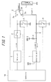
- FIG. 1 is a circuit diagram illustrating a schematic structure of an example of the tactile providing apparatus which the inventor has previously developed.
- a piezoelectric element 1 functions as a load sensor for detecting pressing (pressure) on a contacted surface (not shown) and also as an actuator for providing a tactile sensation by vibrating the contacted surface.
- the piezoelectric element 1 has one electrode connected to a common contact 2a of a changeover switch 2 and the other electrode earthed.
- the changeover switch 2 has two changeover contacts 2b and 2c.
- the changeover contact 2b is connected to a drive unit 4 via a drive switch 3 and, simultaneously, earthed via a discharge switch 5 that constitutes a discharge unit.
- the drive unit 4 is configured to output a drive signal having predetermined waveform, frequency and amplitude (e.g., several 10 V) that correspond to a tactile sensation to be provided.
- the changeover contact 2c is connected to a detection unit 7 via a capacitor 6 used for DC blocking and, simultaneously, earthed via a reset switch 8.
- the detection unit 7 includes an AD converter for converting an analog input voltage into a digital signal and is configured to detect pressing or releasing by detecting a change in the AC converted signal, i.e., a change in a signal equivalent to a change in a voltage of, for example, several 100 mV.
- a predetermined voltage a reference voltage
- the reference voltage is set to, for example, VDD/2 when a power supply voltage of the AD converter is represented by VDD.
- the drive unit 4 and the detection unit 7 are connected to a controller 10 and controlled thereby.
- the changeover switch 2, the drive switch 3, the discharge switch 5, and the reset switch 8 are constituted by using a semiconductor switch such as, for example, an FET and controlled by the controller 10.
- the switchover contact 2c is connected to the common contact 2a when the control signal from the controller 10 is at a low (L) level
- the switchover contact 2b is connected to the common contact 2a when the control signal is at a high (H) level.
- the drive switch 3, the discharge switch 5, and the reset switch 8 are open (OFF) when the control signal from the controller 10 is at the L level and close (ON) when the control signal is at the H level.
- the drive unit 4 and the detection unit 7 may be incorporated in the controller 10.
- FIG. 2 is a timing chart illustrating operations of the tactile sensation providing apparatus illustrated in FIG. 1 that does not take dielectric absorption of the piezoelectric element 1 into consideration.
- a signal 1 represents a terminal voltage of the piezoelectric element 1.
- a signal 2 represents a voltage of the switchover contact 2c.
- a signal 3 represents an input voltage of the detection unit 7.
- the controller 10 normally sets respective control signals of the changeover switch 2, the drive switch 3, the discharge switch 5, and the reset switch 8 to the L level and controls the detection unit 7 to monitor an output voltage of the piezoelectric element 1.
- the controller 10 sets the respective control signals of the changeover switch 2 and the reset switch 8 to the H level.
- the detection unit 7 detects the pressing when detecting an increase in the signal 3 by, for example, several 100 mV relative to the reference voltage.
- the controller 10 sets the control signal of the drive switch 3 to the H level for a predetermined period of time, during which the drive unit 4 applies a drive signal with predetermined frequency and amplitude to the piezoelectric element 1 via the drive switch 3 and the changeover switch 2. Thereby, the piezoelectric element 1 is vibrated and provides a tactile sensation.
- FIG. 2 illustrates an example in which a drive signal of a sine wave at the predetermined frequency with the amplitude of several 10 V is applied to the piezoelectric element 1 for a half cycle.
- the controller 10 sets the control signal of the drive switch 3 to the L level and then control signal of the discharge switch 5 to the H level for the predetermined period of time. Thereby, charge stored in the piezoelectric element 1 is discharged via the changeover switch 2 and the discharge switch 5.
- the controller 10 sets the respective control signals of the discharge switch 5 and the reset switch 8 to the L level and, at time t2, sets the control signal of the changeover switch 2 to the L level and controls the detection unit 7 to start monitoring the output voltage of the piezoelectric element 1. Then, when the detection unit 7 detects releasing of the contact object from the contacted surface at time t3, the controller 10 sets the respective control signals of the changeover switch 2 and the reset switch 8 to the H level and controls each unit in a manner similar to that for the detection of the pressing as described above such that the tactile sensation is provided. Then, the controller 10, at time t4, controls the detection unit 7 to start monitoring the output voltage of the piezoelectric element 1.
- the detection unit 7 detects the releasing when detecting a decrease in the signal 3 by, for example, several 100 mV relative to the reference voltage. Thereafter, by carrying out similar operations, the controller 10 detects next pressing/releasing and provides the tactile sensation at each time of the detection.
- the tactile sensation providing apparatus illustrated in FIG. 1 includes the discharge switch 5 and, after driving the piezoelectric element 1, turns the discharge switch 5 on so as to discharge the piezoelectric element 1.
- the tactile sensation providing apparatus also includes the reset switch 8 and, prior to the monitoring of the output voltage of the piezoelectric element 1 by the detection unit 7, resets the capacitor 6. Therefore, even when the piezoelectric element 1 is sequentially driven, a gradual increase in the input voltage of the detection unit 7 (the signal 3) caused each time the piezoelectric element 1 is driven may be prevented. Therefore, even when the pressing/releasing is continuously iterated, the pressing/releasing may be detected.
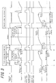
- the piezoelectric element 1 has the dielectric absorption. Therefore, regardless of the discharging operation of the piezoelectric element 1 after the driving thereof, the output voltage of the piezoelectric element 1 thereafter during the voltage monitoring by the detection unit 7 changes as illustrated in FIG. 3 . That is, the output voltage of the piezoelectric element 1 gradually increases from the start of the voltage monitoring and, after, for example, 200 msec to 300 msec, reaches approximately several V, for example.
- the input voltage (the signal 3) of the detection unit 7 significantly decreases from the reference voltage relative to the change in the voltage at the detection of the releasing and then gradually increases toward the reference voltage.
- the signal 3 when the detection unit 7 starts monitoring the voltage becomes lower than the reference voltage.
- This phenomenon occurs due to a sharp decrease in the voltage when the signal 2 increased by the dielectric absorption is reset and, following the decrease in the voltage, the signal 3 also decreases via the capacitor 6 by the same voltage. Note that a change in the signal 3 after the driving of the piezoelectric element 1 in response to the first pressing is cut off by the capacitor 6 due to the increase in the signal 2 caused by the dielectric absorption for several 100 msec. As a result, the signal 3 is maintained at the reference voltage until the releasing causes a change in the voltage.
- the decrease in the input voltage of the detection unit 7 due to the dielectric absorption needs to be taken into consideration.
- the decrease in the input voltage due to the dielectric absorption varies depending on operation timings of the pressing/releasing and the like.
- the disclosure herein intends to solve such problems and provide a tactile sensation providing apparatus and a control method therefor that have a simple configuration and are capable of, without being affected by the dielectric absorption of the piezoelectric element, reliably detecting the pressing/releasing and providing the tactile sensation.
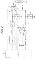
- FIG. 4 is a circuit diagram illustrating a schematic configuration of a tactile sensation providing apparatus according to one embodiment.
- the tactile sensation providing apparatus of the present embodiment includes the circuit configuration illustrated in FIG. 1 having a voltage application switch 11 in parallel connection with the pull-up resistor 9 connected to the input terminal of the detection unit 7.
- the voltage application switch 11 constitutes a voltage fixing unit and is constituted by using, similarly to other switches, the semiconductor switch such as the FET so as to be turned off in response to the control signal at the L level from the controller 10 and to be turned on in response to the control signal at the H level.
- Other configurations of the tactile sensation providing apparatus is similar to that of FIG. 1 .
- FIG 5 is a timing chart illustrating an examples of operations of the tactile sensation providing apparatus of FIG. 4 .
- the voltage application switch 11 is turned on/off at the same timing as the reset switch 8. Therefore, when the reset switch 8 and the voltage application switch 11 are turned on at the time t3 at which the first releasing is detected, the reference voltage (for example, the VDD/2) is directly applied to the input terminal of the detection unit 7, i.e., one of the electrodes of the capacitor 6, and the other electrode of the capacitor 6 is earthed via the reset switch 8.
- the reference voltage for example, the VDD/2
- the input voltage (the signal 3) of the detection unit 7 is fixed (held) at the reference voltage by the direct application of the reference voltage.
- the signal 3 is at the reference voltage when the detection unit 7 starts monitoring the voltage, allowing the detection of the second pressing based on a change in the signal 3 from the reference voltage.
- the second releasing and subsequent pressing/releasing may be also detected in a similar manner based on the change in the signal 3 from the reference voltage.
- the tactile sensation providing apparatus after the detection of the pressing or releasing by the detection unit 7 before the start of the detection of the next releasing or pressing, the voltage application switch 11 and the reset switch 8 are turned on and the input voltage (the signal 3) of the detection unit 7 is fixed at the reference voltage (e.g., the VDD/2). Accordingly, without increasing the software processing, a simple configuration may be achieved that is capable of, without being affected by the dielectric absorption of the piezoelectric element 1, reliably detecting the pressing/releasing and providing the tactile sensation.
- the reference voltage e.g., the VDD/2
- the voltage application switch 11 does not necessarily need to be turned on/off at the same timing as the reset switch 8 but may be turned on while the reset switch 8 is ON.
- the discharge switch 5 may be connected between the common contact 2a of the changeover switch 2 and one of the electrodes of the piezoelectric element 1. In this case, for example, the piezoelectric element 1 is discharged after being driven while being connected to the changeover contact 2b of the changeover switch 2, and the changeover switch 2 is connected to the changeover contact 2c and the voltage application switch 11 is turned on while the discharge switch 5 is on. Thereby, the reset switch 8 may be omitted.
- modules and/or units are schematically illustrated to explain functionalities thereof and do not necessarily illustrate specific hardware and/or software.
- these modules, units, and other components may be any hardware and/or software implemented to substantially perform the specific functions described herein.
- Various functions of the respective components may be achieved by the hardware and/or the software combined or separated in any manners, and these separated or combined hardware and/or software may be used separately or in any combination thereof. In this way, various aspects of the disclosure herein may be carried out in numerous different modes, and therefore all of those modes are included in the scope of the disclosure herein.
Landscapes
- Engineering & Computer Science (AREA)
- General Engineering & Computer Science (AREA)
- Theoretical Computer Science (AREA)
- Human Computer Interaction (AREA)
- Physics & Mathematics (AREA)
- General Physics & Mathematics (AREA)
- User Interface Of Digital Computer (AREA)
- Apparatuses For Generation Of Mechanical Vibrations (AREA)
Abstract
Description
- This application claims priority to and the benefit of Japanese Patent Application No.
2013-223276 filed on October 28, 2013 - The present invention relates to tactile sensation providing apparatus and a control method of the tactile sensation providing apparatus.
- Conventionally, there has been known a technique to provide, on a contacted surface such as a touch panel, a realistic tactile sensation to a contact object such as a finger (for example, see PLT 1). In the technology disclosed in the
PLT 1, a piezoelectric element is commonly used as a load sensor for detecting pressing (depression) to the contacted surface and also as an actuator for vibrating the contacted surface. When the piezoelectric element functions as the load sensor and detects a predetermined load (output voltage) generated by a pressing operation of the contact object to the contacted surface, the piezoelectric element is controlled to function as the actuator for a predetermined period of time and to vibrate the contacted surface. Similarly, upon detection of the predetermined output voltage generated by a releasing operation of the contact object from the contacted surface, the piezoelectric element is controlled to function as the actuator for a predetermined period of time and to vibrate the contacted surface. - PLT 1:
JP4672075B2 - Incidentally, the piezoelectric element is known to have characteristics called dielectric absorption (dielectric hysteresis) in which the piezoelectric element presents a voltage even when the piezoelectric element is discharged after vibrated upon application of the voltage. Therefore, in order to reliably provide the tactile sensation at the time of pressing/releasing by using the piezoelectric element as the load sensor and also as the actuator, the dielectric absorption needs to be taken into consideration.
- In view of the above aspects, it could be helpful to provide a tactile sensation providing apparatus and a control method of the tactile sensation providing apparatus that have a simple configuration and are capable of, without being affected by the dielectric absorption of the piezoelectric element, reliably detecting the pressing/releasing and providing the tactile sensation.
- In order to achieve the above object, a tactile sensation providing apparatus includes:
- a piezoelectric element;
- a detection unit for detecting each pressing and releasing based on an output voltage of the piezoelectric element;
- a drive unit for driving the piezoelectric element synchronously with the detection of each pressing and releasing by the detection unit and thereby providing a tactile sensation;
- a discharge unit for discharging the piezoelectric element after the driving of the piezoelectric element before start of detection of next releasing or pressing; and
- a voltage fixing unit for fixing an input voltage of the detection unit at a predetermined voltage after the detection of the pressing or releasing by the detection unit before the start of the detection of the next releasing or pressing.
- In order to achieve the above object, further, a control method of a tactile sensation providing apparatus having
a piezoelectric element,
a detection unit for detecting each pressing and releasing based on an output voltage of the piezoelectric element,
a drive unit for driving the piezoelectric element synchronously with the detection of each pressing and releasing by the detection unit and thereby providing a tactile sensation,
a discharge unit for discharging the piezoelectric element after the driving of the piezoelectric element before start of detection of next releasing or pressing, and
a voltage fixing unit for fixing an input voltage of the detection unit at a predetermined voltage, the control method includes: - after the detection of the pressing or releasing by the detection unit before the start of the detection of the next releasing or pressing, fixing the input voltage of the detection unit at the predetermined voltage by the voltage fixing unit.
- According to the disclosure herein, the tactile sensation may be provided by reliably detecting pressing/releasing with a simple structure without being affected by dielectric absorption of the piezoelectric element.
- In the accompanying drawings:
-
FIG. 1 is a circuit diagram illustrating an example of a schematic structure of a tactile sensation providing apparatus; -
FIG. 2 is a timing chart illustrating operations of the tactile sensation providing apparatus ofFIG. 1 ; -
FIG. 3 is an explanatory view of a problem to be solved by the disclosure herein; -
FIG. 4 is a circuit diagram illustrating a schematic structure of a tactile sensation providing apparatus according to one embodiment; and -
FIG. 5 is a timing chart illustrating an example of operations of the tactile sensation providing apparatus ofFIG. 4 . - First, prior to a description of one embodiment, a tactile sensation providing apparatus which the inventor has previously developed will be described.
-
FIG. 1 is a circuit diagram illustrating a schematic structure of an example of the tactile providing apparatus which the inventor has previously developed. InFIG 1 , apiezoelectric element 1 functions as a load sensor for detecting pressing (pressure) on a contacted surface (not shown) and also as an actuator for providing a tactile sensation by vibrating the contacted surface. Thepiezoelectric element 1 has one electrode connected to acommon contact 2a of achangeover switch 2 and the other electrode earthed. Thechangeover switch 2 has twochangeover contacts - The
changeover contact 2b is connected to adrive unit 4 via adrive switch 3 and, simultaneously, earthed via adischarge switch 5 that constitutes a discharge unit. Thedrive unit 4 is configured to output a drive signal having predetermined waveform, frequency and amplitude (e.g., several 10 V) that correspond to a tactile sensation to be provided. On the other hand, thechangeover contact 2c is connected to adetection unit 7 via acapacitor 6 used for DC blocking and, simultaneously, earthed via areset switch 8. Thedetection unit 7 includes an AD converter for converting an analog input voltage into a digital signal and is configured to detect pressing or releasing by detecting a change in the AC converted signal, i.e., a change in a signal equivalent to a change in a voltage of, for example, several 100 mV. To an input terminal of thedetection unit 7, a predetermined voltage (a reference voltage) is applied via a pull-up resistor 9. The reference voltage is set to, for example, VDD/2 when a power supply voltage of the AD converter is represented by VDD. - The
drive unit 4 and thedetection unit 7 are connected to acontroller 10 and controlled thereby. Also, thechangeover switch 2, thedrive switch 3, thedischarge switch 5, and thereset switch 8 are constituted by using a semiconductor switch such as, for example, an FET and controlled by thecontroller 10. For example, in thechangeover switch 2, theswitchover contact 2c is connected to thecommon contact 2a when the control signal from thecontroller 10 is at a low (L) level, while theswitchover contact 2b is connected to thecommon contact 2a when the control signal is at a high (H) level. Further, thedrive switch 3, thedischarge switch 5, and thereset switch 8 are open (OFF) when the control signal from thecontroller 10 is at the L level and close (ON) when the control signal is at the H level. Note that thedrive unit 4 and thedetection unit 7 may be incorporated in thecontroller 10. -
FIG. 2 is a timing chart illustrating operations of the tactile sensation providing apparatus illustrated inFIG. 1 that does not take dielectric absorption of thepiezoelectric element 1 into consideration. InFIG. 2 , asignal 1 represents a terminal voltage of thepiezoelectric element 1. Asignal 2 represents a voltage of theswitchover contact 2c. Asignal 3 represents an input voltage of thedetection unit 7. Thecontroller 10 normally sets respective control signals of thechangeover switch 2, thedrive switch 3, thedischarge switch 5, and thereset switch 8 to the L level and controls thedetection unit 7 to monitor an output voltage of thepiezoelectric element 1. When thedetection unit 7 detects pressing on the contacted surface by a contact object at time t1, thecontroller 10 sets the respective control signals of thechangeover switch 2 and thereset switch 8 to the H level. Thedetection unit 7 detects the pressing when detecting an increase in thesignal 3 by, for example, several 100 mV relative to the reference voltage. - When the pressing is detected, the
controller 10 sets the control signal of thedrive switch 3 to the H level for a predetermined period of time, during which thedrive unit 4 applies a drive signal with predetermined frequency and amplitude to thepiezoelectric element 1 via thedrive switch 3 and thechangeover switch 2. Thereby, thepiezoelectric element 1 is vibrated and provides a tactile sensation.FIG. 2 illustrates an example in which a drive signal of a sine wave at the predetermined frequency with the amplitude of several 10 V is applied to thepiezoelectric element 1 for a half cycle. Subsequently, thecontroller 10 sets the control signal of thedrive switch 3 to the L level and then control signal of thedischarge switch 5 to the H level for the predetermined period of time. Thereby, charge stored in thepiezoelectric element 1 is discharged via thechangeover switch 2 and thedischarge switch 5. - Next, the
controller 10 sets the respective control signals of thedischarge switch 5 and thereset switch 8 to the L level and, at time t2, sets the control signal of thechangeover switch 2 to the L level and controls thedetection unit 7 to start monitoring the output voltage of thepiezoelectric element 1. Then, when thedetection unit 7 detects releasing of the contact object from the contacted surface at time t3, thecontroller 10 sets the respective control signals of thechangeover switch 2 and thereset switch 8 to the H level and controls each unit in a manner similar to that for the detection of the pressing as described above such that the tactile sensation is provided. Then, thecontroller 10, at time t4, controls thedetection unit 7 to start monitoring the output voltage of thepiezoelectric element 1. Thedetection unit 7 detects the releasing when detecting a decrease in thesignal 3 by, for example, several 100 mV relative to the reference voltage. Thereafter, by carrying out similar operations, thecontroller 10 detects next pressing/releasing and provides the tactile sensation at each time of the detection. - The tactile sensation providing apparatus illustrated in
FIG. 1 includes thedischarge switch 5 and, after driving thepiezoelectric element 1, turns thedischarge switch 5 on so as to discharge thepiezoelectric element 1. The tactile sensation providing apparatus also includes thereset switch 8 and, prior to the monitoring of the output voltage of thepiezoelectric element 1 by thedetection unit 7, resets thecapacitor 6. Therefore, even when thepiezoelectric element 1 is sequentially driven, a gradual increase in the input voltage of the detection unit 7 (the signal 3) caused each time thepiezoelectric element 1 is driven may be prevented. Therefore, even when the pressing/releasing is continuously iterated, the pressing/releasing may be detected. - In practice, however, the
piezoelectric element 1 has the dielectric absorption. Therefore, regardless of the discharging operation of thepiezoelectric element 1 after the driving thereof, the output voltage of thepiezoelectric element 1 thereafter during the voltage monitoring by thedetection unit 7 changes as illustrated inFIG. 3 . That is, the output voltage of thepiezoelectric element 1 gradually increases from the start of the voltage monitoring and, after, for example, 200 msec to 300 msec, reaches approximately several V, for example. Therefore, after thepiezoelectric element 1 is driven in response to the detection of the first pressing (first pressing detection) at the time t1, when thereset switch 8 is turned on in response to the detection of the releasing at the time t3 (first releasing detection), the input voltage (the signal 3) of thedetection unit 7 significantly decreases from the reference voltage relative to the change in the voltage at the detection of the releasing and then gradually increases toward the reference voltage. As a result, after the time t4, thesignal 3 when thedetection unit 7 starts monitoring the voltage becomes lower than the reference voltage. - This phenomenon occurs due to a sharp decrease in the voltage when the
signal 2 increased by the dielectric absorption is reset and, following the decrease in the voltage, thesignal 3 also decreases via thecapacitor 6 by the same voltage. Note that a change in thesignal 3 after the driving of thepiezoelectric element 1 in response to the first pressing is cut off by thecapacitor 6 due to the increase in thesignal 2 caused by the dielectric absorption for several 100 msec. As a result, thesignal 3 is maintained at the reference voltage until the releasing causes a change in the voltage. - Therefore, at the detection of second and subsequent pressing/releasing, the decrease in the input voltage of the
detection unit 7 due to the dielectric absorption needs to be taken into consideration. However, the decrease in the input voltage due to the dielectric absorption varies depending on operation timings of the pressing/releasing and the like. Further, at the pressing/releasing, it is necessary to detect, with respect to a voltage fluctuation of several V due to the dielectric absorption, a change in the voltage as small as several 100 mV. Therefore, the detection of the pressing/releasing while taking an impact of the voltage fluctuation of thesignal 3 due to the dielectric absorption into consideration may render software processing troublesome by increasing the number thereof and, also, cause an erroneous detection. - The disclosure herein intends to solve such problems and provide a tactile sensation providing apparatus and a control method therefor that have a simple configuration and are capable of, without being affected by the dielectric absorption of the piezoelectric element, reliably detecting the pressing/releasing and providing the tactile sensation.
-
FIG. 4 is a circuit diagram illustrating a schematic configuration of a tactile sensation providing apparatus according to one embodiment. The tactile sensation providing apparatus of the present embodiment includes the circuit configuration illustrated inFIG. 1 having avoltage application switch 11 in parallel connection with the pull-upresistor 9 connected to the input terminal of thedetection unit 7. Thevoltage application switch 11 constitutes a voltage fixing unit and is constituted by using, similarly to other switches, the semiconductor switch such as the FET so as to be turned off in response to the control signal at the L level from thecontroller 10 and to be turned on in response to the control signal at the H level. Other configurations of the tactile sensation providing apparatus is similar to that ofFIG. 1 . -
FIG 5 is a timing chart illustrating an examples of operations of the tactile sensation providing apparatus ofFIG. 4 . In the example of operations illustrated inFIG. 5 , thevoltage application switch 11 is turned on/off at the same timing as thereset switch 8. Therefore, when thereset switch 8 and thevoltage application switch 11 are turned on at the time t3 at which the first releasing is detected, the reference voltage (for example, the VDD/2) is directly applied to the input terminal of thedetection unit 7, i.e., one of the electrodes of thecapacitor 6, and the other electrode of thecapacitor 6 is earthed via thereset switch 8. - Thus, at time t3, even when the
signal 2 increases due to the dielectric absorption of thepiezoelectric element 1, the input voltage (the signal 3) of thedetection unit 7 is fixed (held) at the reference voltage by the direct application of the reference voltage. At the time t4, as a result, thesignal 3 is at the reference voltage when thedetection unit 7 starts monitoring the voltage, allowing the detection of the second pressing based on a change in thesignal 3 from the reference voltage. The second releasing and subsequent pressing/releasing may be also detected in a similar manner based on the change in thesignal 3 from the reference voltage. - As described above, the tactile sensation providing apparatus according to the present embodiment, after the detection of the pressing or releasing by the
detection unit 7 before the start of the detection of the next releasing or pressing, thevoltage application switch 11 and thereset switch 8 are turned on and the input voltage (the signal 3) of thedetection unit 7 is fixed at the reference voltage (e.g., the VDD/2). Accordingly, without increasing the software processing, a simple configuration may be achieved that is capable of, without being affected by the dielectric absorption of thepiezoelectric element 1, reliably detecting the pressing/releasing and providing the tactile sensation. - Note that the disclosure herein is not limited to the above embodiment but may be varied or modified in numerous manners. For example, the
voltage application switch 11 does not necessarily need to be turned on/off at the same timing as thereset switch 8 but may be turned on while thereset switch 8 is ON. Also, thedischarge switch 5 may be connected between thecommon contact 2a of thechangeover switch 2 and one of the electrodes of thepiezoelectric element 1. In this case, for example, thepiezoelectric element 1 is discharged after being driven while being connected to thechangeover contact 2b of thechangeover switch 2, and thechangeover switch 2 is connected to thechangeover contact 2c and thevoltage application switch 11 is turned on while thedischarge switch 5 is on. Thereby, thereset switch 8 may be omitted. - Further, although the above embodiment discloses a configuration having various modules and/or units for performing specific functions, these modules and/or units are schematically illustrated to explain functionalities thereof and do not necessarily illustrate specific hardware and/or software. In that sense, these modules, units, and other components may be any hardware and/or software implemented to substantially perform the specific functions described herein. Various functions of the respective components may be achieved by the hardware and/or the software combined or separated in any manners, and these separated or combined hardware and/or software may be used separately or in any combination thereof In this way, various aspects of the disclosure herein may be carried out in numerous different modes, and therefore all of those modes are included in the scope of the disclosure herein.
-
- 1
- piezoelectric element
- 2
- changeover switch
- 3
- drive switch
- 4
- drive unit
- 5
- discharge switch
- 6
- capacitor
- 7
- detection unit
- 8
- reset switch
- 9
- pull-up resistor
- 10
- controller
- 11
- voltage application switch
Claims (2)
- A tactile sensation providing apparatus comprising:a piezoelectric element;a detection unit for detecting each pressing and releasing based on an output voltage of the piezoelectric element;a drive unit for driving the piezoelectric element synchronously with the detection of each pressing and releasing by the detection unit and thereby providing a tactile sensation;a discharge unit for discharging the piezoelectric element after the driving of the piezoelectric element before start of detection of next releasing or pressing; anda voltage fixing unit for fixing an input voltage of the detection unit at a predetermined voltage after the detection of the pressing or releasing by the detection unit before the start of the detection of the next releasing or pressing.
- A control method of a tactile sensation providing apparatus having
a piezoelectric element,
a detection unit for detecting each pressing and releasing based on an output voltage of the piezoelectric element,
a drive unit for driving the piezoelectric element synchronously with the detection of each pressing and releasing by the detection unit and thus providing a tactile sensation,
a discharge unit for discharging the piezoelectric element after the driving of the piezoelectric element before start of detection of next releasing or pressing, and
a voltage fixing unit for fixing an input voltage of the detection unit at a predetermined voltage, the control method comprising:after the detection of the pressing or releasing by the detection unit before the start of the detection of the next releasing or pressing, fixing the input voltage of the detection unit at the predetermined voltage by the voltage fixing unit.
Applications Claiming Priority (2)
| Application Number | Priority Date | Filing Date | Title |
|---|---|---|---|
| JP2013223276 | 2013-10-28 | ||
| PCT/JP2014/004941 WO2015064007A1 (en) | 2013-10-28 | 2014-09-26 | Tactile sensation presentation device and method for controlling tactile sensation presentation device |
Publications (3)
| Publication Number | Publication Date |
|---|---|
| EP3065029A1 true EP3065029A1 (en) | 2016-09-07 |
| EP3065029A4 EP3065029A4 (en) | 2017-06-21 |
| EP3065029B1 EP3065029B1 (en) | 2019-06-12 |
Family
ID=53003643
Family Applications (1)
| Application Number | Title | Priority Date | Filing Date |
|---|---|---|---|
| EP14857388.4A Active EP3065029B1 (en) | 2013-10-28 | 2014-09-26 | Tactile sensation presentation device and method for controlling tactile sensation presentation device |
Country Status (4)
| Country | Link |
|---|---|
| US (1) | US10031584B2 (en) |
| EP (1) | EP3065029B1 (en) |
| JP (1) | JP6100913B2 (en) |
| WO (1) | WO2015064007A1 (en) |
Cited By (6)
| Publication number | Priority date | Publication date | Assignee | Title |
|---|---|---|---|---|
| WO2018141962A1 (en) * | 2017-02-06 | 2018-08-09 | Aito Interactive Oy | Haptic signalizing device |
| WO2018172220A1 (en) | 2017-03-22 | 2018-09-27 | Epcos Ag | Driver circuit for analyzing and controlling a piezoelectric component, button providing haptic feedback, and operating method |
| EP3627704A1 (en) * | 2018-09-20 | 2020-03-25 | Boréas Technologies Inc. | Zero-power wake-up sensing circuit in piezoelectric haptic feedback |
| CN111065990A (en) * | 2017-09-11 | 2020-04-24 | 富士通株式会社 | Control device, electronic device, and control method for electronic device |
| EP3917010A1 (en) | 2020-05-28 | 2021-12-01 | Boréas Technologies Inc. | High-resolution sensing of piezo-electric transducers |
| DE102023104733B3 (en) | 2023-02-27 | 2024-06-27 | Tdk Electronics Ag | Analog driver circuit for piezo components and control unit |
Family Cites Families (11)
| Publication number | Priority date | Publication date | Assignee | Title |
|---|---|---|---|---|
| JPH09178472A (en) | 1995-12-27 | 1997-07-11 | Olympus Optical Co Ltd | Range finder |
| JP2011048696A (en) | 2009-08-27 | 2011-03-10 | Kyocera Corp | Input device |
| JP4672075B2 (en) | 2009-08-27 | 2011-04-20 | 京セラ株式会社 | Input device |
| US8744803B2 (en) * | 2010-09-30 | 2014-06-03 | Fitbit, Inc. | Methods, systems and devices for activity tracking device data synchronization with computing devices |
| WO2013105517A1 (en) * | 2012-01-13 | 2013-07-18 | 京セラ株式会社 | Electronic apparatus, and method for controlling electronic apparatus |
| JPWO2013105516A1 (en) * | 2012-01-13 | 2015-05-11 | 京セラ株式会社 | Electronic device and control method of electronic device |
| KR102169952B1 (en) * | 2013-10-18 | 2020-10-26 | 엘지전자 주식회사 | Wearable device and method of controlling thereof |
| US20150293590A1 (en) * | 2014-04-11 | 2015-10-15 | Nokia Corporation | Method, Apparatus, And Computer Program Product For Haptically Providing Information Via A Wearable Device |
| US9232331B2 (en) * | 2014-05-08 | 2016-01-05 | Microsoft Technology Licensing, Llc | Hand-worn device for surface gesture input |
| WO2016012835A1 (en) * | 2014-07-23 | 2016-01-28 | What Watch Ag | Wristwatch device with time management function |
| JP2016038905A (en) * | 2014-08-08 | 2016-03-22 | パナソニックIpマネジメント株式会社 | Input device and device control method |
-
2014
- 2014-09-26 JP JP2015544773A patent/JP6100913B2/en active Active
- 2014-09-26 EP EP14857388.4A patent/EP3065029B1/en active Active
- 2014-09-26 US US15/031,817 patent/US10031584B2/en active Active
- 2014-09-26 WO PCT/JP2014/004941 patent/WO2015064007A1/en not_active Ceased
Cited By (16)
| Publication number | Priority date | Publication date | Assignee | Title |
|---|---|---|---|---|
| US10852834B2 (en) | 2017-02-06 | 2020-12-01 | Aito Bv | Haptic signalizing device |
| CN110582739A (en) * | 2017-02-06 | 2019-12-17 | 艾托有限公司 | Tactile signaling device |
| CN110582739B (en) * | 2017-02-06 | 2023-07-25 | 艾托有限公司 | Tactile signaling device |
| WO2018141962A1 (en) * | 2017-02-06 | 2018-08-09 | Aito Interactive Oy | Haptic signalizing device |
| US11223356B2 (en) | 2017-03-22 | 2022-01-11 | Tdk Electronics Ag | Driver circuit for analyzing and controlling a piezoelectric component, button providing haptic feedback, and operating method |
| WO2018172220A1 (en) | 2017-03-22 | 2018-09-27 | Epcos Ag | Driver circuit for analyzing and controlling a piezoelectric component, button providing haptic feedback, and operating method |
| DE212018000085U1 (en) | 2017-03-22 | 2019-05-23 | Tdk Electronics Ag | Driver circuit for evaluation and control of a piezoelectric device and button with haptic feedback |
| DE102017106188B3 (en) | 2017-03-22 | 2018-09-27 | Epcos Ag | Driver circuit for evaluation and control of a piezoelectric device, button with haptic feedback and operating method |
| EP3683660A4 (en) * | 2017-09-11 | 2020-09-02 | Fujitsu Limited | CONTROL DEVICE, ELECTRONIC DEVICE AND CONTROL METHOD FOR ELECTRONIC DEVICE |
| CN111065990A (en) * | 2017-09-11 | 2020-04-24 | 富士通株式会社 | Control device, electronic device, and control method for electronic device |
| US11561653B2 (en) | 2017-09-11 | 2023-01-24 | Fujitsu Limited | Control circuitry, electronic device, and method for controlling electronic device |
| EP3627704A1 (en) * | 2018-09-20 | 2020-03-25 | Boréas Technologies Inc. | Zero-power wake-up sensing circuit in piezoelectric haptic feedback |
| US11302859B2 (en) | 2018-09-20 | 2022-04-12 | Boréas Technologies Inc. | Zero-power wake-up sensing circuit in piezoelectric haptic feedback |
| EP3917010A1 (en) | 2020-05-28 | 2021-12-01 | Boréas Technologies Inc. | High-resolution sensing of piezo-electric transducers |
| DE102023104733B3 (en) | 2023-02-27 | 2024-06-27 | Tdk Electronics Ag | Analog driver circuit for piezo components and control unit |
| WO2024179817A1 (en) | 2023-02-27 | 2024-09-06 | Tdk Electronics Ag | Analogue driver circuit for piezo components, and control unit |
Also Published As
| Publication number | Publication date |
|---|---|
| JP6100913B2 (en) | 2017-03-22 |
| JPWO2015064007A1 (en) | 2017-03-09 |
| EP3065029B1 (en) | 2019-06-12 |
| US10031584B2 (en) | 2018-07-24 |
| EP3065029A4 (en) | 2017-06-21 |
| WO2015064007A1 (en) | 2015-05-07 |
| US20160246372A1 (en) | 2016-08-25 |
Similar Documents
| Publication | Publication Date | Title |
|---|---|---|
| EP3065029B1 (en) | Tactile sensation presentation device and method for controlling tactile sensation presentation device | |
| US9000690B2 (en) | Driver for capacitive loads | |
| US9513709B2 (en) | Haptic feedback generation based on resonant frequency | |
| CN102483663A (en) | Input device | |
| US9054627B2 (en) | Method and apparatus to drive a linear resonant actuator at its resonant frequency | |
| EP3668111A1 (en) | Mute control circuit used upon power-on or power-of, control method, and audio device | |
| US10444837B2 (en) | Tactile sensation providing apparatus | |
| US10984693B2 (en) | Display device and shutdown control method thereof | |
| US8847896B2 (en) | Adaptive high dynamic range surface capacitive touchscreen controller | |
| US20150378511A1 (en) | Capacitive Voltage Information Sensing Circuit and Related Anti-Noise Touch Circuit | |
| CN114207555B (en) | Control device, control method and control program | |
| US10725546B2 (en) | Tactile presentation device and touch panel | |
| CN111656271A (en) | Anti-peep circuit and driving method thereof, and display device | |
| JP2018133892A5 (en) | ||
| KR101718080B1 (en) | Apparatus for driving light emitting diode with key scan function and method for controlling thereof | |
| JP2005158870A5 (en) | ||
| KR101997519B1 (en) | A touch sensing device for removing sensing errors occurred by noise from a display panel and fabrication variation | |
| CN111552208A (en) | A state control circuit, method and device | |
| CN116893326A (en) | Gate drive circuit, test device and switching method | |
| JP2007163301A (en) | Burn-in test signal generation circuit and burn-in test method | |
| JP2014191516A (en) | Resistance film type touch panel device | |
| KR20180015367A (en) | Switching Control circuit of pulse power supply | |
| KR20200037683A (en) | Improving signal to noise ratio method of capacitive sensors including LED driver | |
| CN103748789B (en) | Capacitive sensor device and the method for calibration capacitance sensor device | |
| TWI586971B (en) | Measurement and feedback circuit, measurement and feedback keyswitch, and measurement and feedback method |
Legal Events
| Date | Code | Title | Description |
|---|---|---|---|
| PUAI | Public reference made under article 153(3) epc to a published international application that has entered the european phase |
Free format text: ORIGINAL CODE: 0009012 |
|
| 17P | Request for examination filed |
Effective date: 20160427 |
|
| AK | Designated contracting states |
Kind code of ref document: A1 Designated state(s): AL AT BE BG CH CY CZ DE DK EE ES FI FR GB GR HR HU IE IS IT LI LT LU LV MC MK MT NL NO PL PT RO RS SE SI SK SM TR |
|
| AX | Request for extension of the european patent |
Extension state: BA ME |
|
| DAX | Request for extension of the european patent (deleted) | ||
| A4 | Supplementary search report drawn up and despatched |
Effective date: 20170518 |
|
| RIC1 | Information provided on ipc code assigned before grant |
Ipc: G06F 3/01 20060101AFI20170512BHEP Ipc: G06F 3/041 20060101ALI20170512BHEP |
|
| STAA | Information on the status of an ep patent application or granted ep patent |
Free format text: STATUS: EXAMINATION IS IN PROGRESS |
|
| 17Q | First examination report despatched |
Effective date: 20180511 |
|
| GRAP | Despatch of communication of intention to grant a patent |
Free format text: ORIGINAL CODE: EPIDOSNIGR1 |
|
| STAA | Information on the status of an ep patent application or granted ep patent |
Free format text: STATUS: GRANT OF PATENT IS INTENDED |
|
| INTG | Intention to grant announced |
Effective date: 20190125 |
|
| GRAS | Grant fee paid |
Free format text: ORIGINAL CODE: EPIDOSNIGR3 |
|
| GRAA | (expected) grant |
Free format text: ORIGINAL CODE: 0009210 |
|
| STAA | Information on the status of an ep patent application or granted ep patent |
Free format text: STATUS: THE PATENT HAS BEEN GRANTED |
|
| AK | Designated contracting states |
Kind code of ref document: B1 Designated state(s): AL AT BE BG CH CY CZ DE DK EE ES FI FR GB GR HR HU IE IS IT LI LT LU LV MC MK MT NL NO PL PT RO RS SE SI SK SM TR |
|
| REG | Reference to a national code |
Ref country code: GB Ref legal event code: FG4D |
|
| REG | Reference to a national code |
Ref country code: CH Ref legal event code: EP |
|
| REG | Reference to a national code |
Ref country code: AT Ref legal event code: REF Ref document number: 1143419 Country of ref document: AT Kind code of ref document: T Effective date: 20190615 |
|
| REG | Reference to a national code |
Ref country code: DE Ref legal event code: R096 Ref document number: 602014048389 Country of ref document: DE |
|
| REG | Reference to a national code |
Ref country code: IE Ref legal event code: FG4D |
|
| REG | Reference to a national code |
Ref country code: NL Ref legal event code: MP Effective date: 20190612 |
|
| REG | Reference to a national code |
Ref country code: LT Ref legal event code: MG4D |
|
| PG25 | Lapsed in a contracting state [announced via postgrant information from national office to epo] |
Ref country code: NO Free format text: LAPSE BECAUSE OF FAILURE TO SUBMIT A TRANSLATION OF THE DESCRIPTION OR TO PAY THE FEE WITHIN THE PRESCRIBED TIME-LIMIT Effective date: 20190912 Ref country code: HR Free format text: LAPSE BECAUSE OF FAILURE TO SUBMIT A TRANSLATION OF THE DESCRIPTION OR TO PAY THE FEE WITHIN THE PRESCRIBED TIME-LIMIT Effective date: 20190612 Ref country code: SE Free format text: LAPSE BECAUSE OF FAILURE TO SUBMIT A TRANSLATION OF THE DESCRIPTION OR TO PAY THE FEE WITHIN THE PRESCRIBED TIME-LIMIT Effective date: 20190612 Ref country code: FI Free format text: LAPSE BECAUSE OF FAILURE TO SUBMIT A TRANSLATION OF THE DESCRIPTION OR TO PAY THE FEE WITHIN THE PRESCRIBED TIME-LIMIT Effective date: 20190612 Ref country code: AL Free format text: LAPSE BECAUSE OF FAILURE TO SUBMIT A TRANSLATION OF THE DESCRIPTION OR TO PAY THE FEE WITHIN THE PRESCRIBED TIME-LIMIT Effective date: 20190612 Ref country code: LT Free format text: LAPSE BECAUSE OF FAILURE TO SUBMIT A TRANSLATION OF THE DESCRIPTION OR TO PAY THE FEE WITHIN THE PRESCRIBED TIME-LIMIT Effective date: 20190612 |
|
| PG25 | Lapsed in a contracting state [announced via postgrant information from national office to epo] |
Ref country code: BG Free format text: LAPSE BECAUSE OF FAILURE TO SUBMIT A TRANSLATION OF THE DESCRIPTION OR TO PAY THE FEE WITHIN THE PRESCRIBED TIME-LIMIT Effective date: 20190912 Ref country code: LV Free format text: LAPSE BECAUSE OF FAILURE TO SUBMIT A TRANSLATION OF THE DESCRIPTION OR TO PAY THE FEE WITHIN THE PRESCRIBED TIME-LIMIT Effective date: 20190612 Ref country code: RS Free format text: LAPSE BECAUSE OF FAILURE TO SUBMIT A TRANSLATION OF THE DESCRIPTION OR TO PAY THE FEE WITHIN THE PRESCRIBED TIME-LIMIT Effective date: 20190612 Ref country code: GR Free format text: LAPSE BECAUSE OF FAILURE TO SUBMIT A TRANSLATION OF THE DESCRIPTION OR TO PAY THE FEE WITHIN THE PRESCRIBED TIME-LIMIT Effective date: 20190913 |
|
| REG | Reference to a national code |
Ref country code: AT Ref legal event code: MK05 Ref document number: 1143419 Country of ref document: AT Kind code of ref document: T Effective date: 20190612 |
|
| PG25 | Lapsed in a contracting state [announced via postgrant information from national office to epo] |
Ref country code: SK Free format text: LAPSE BECAUSE OF FAILURE TO SUBMIT A TRANSLATION OF THE DESCRIPTION OR TO PAY THE FEE WITHIN THE PRESCRIBED TIME-LIMIT Effective date: 20190612 Ref country code: RO Free format text: LAPSE BECAUSE OF FAILURE TO SUBMIT A TRANSLATION OF THE DESCRIPTION OR TO PAY THE FEE WITHIN THE PRESCRIBED TIME-LIMIT Effective date: 20190612 Ref country code: EE Free format text: LAPSE BECAUSE OF FAILURE TO SUBMIT A TRANSLATION OF THE DESCRIPTION OR TO PAY THE FEE WITHIN THE PRESCRIBED TIME-LIMIT Effective date: 20190612 Ref country code: AT Free format text: LAPSE BECAUSE OF FAILURE TO SUBMIT A TRANSLATION OF THE DESCRIPTION OR TO PAY THE FEE WITHIN THE PRESCRIBED TIME-LIMIT Effective date: 20190612 Ref country code: NL Free format text: LAPSE BECAUSE OF FAILURE TO SUBMIT A TRANSLATION OF THE DESCRIPTION OR TO PAY THE FEE WITHIN THE PRESCRIBED TIME-LIMIT Effective date: 20190612 Ref country code: CZ Free format text: LAPSE BECAUSE OF FAILURE TO SUBMIT A TRANSLATION OF THE DESCRIPTION OR TO PAY THE FEE WITHIN THE PRESCRIBED TIME-LIMIT Effective date: 20190612 Ref country code: PT Free format text: LAPSE BECAUSE OF FAILURE TO SUBMIT A TRANSLATION OF THE DESCRIPTION OR TO PAY THE FEE WITHIN THE PRESCRIBED TIME-LIMIT Effective date: 20191014 |
|
| PG25 | Lapsed in a contracting state [announced via postgrant information from national office to epo] |
Ref country code: SM Free format text: LAPSE BECAUSE OF FAILURE TO SUBMIT A TRANSLATION OF THE DESCRIPTION OR TO PAY THE FEE WITHIN THE PRESCRIBED TIME-LIMIT Effective date: 20190612 Ref country code: IS Free format text: LAPSE BECAUSE OF FAILURE TO SUBMIT A TRANSLATION OF THE DESCRIPTION OR TO PAY THE FEE WITHIN THE PRESCRIBED TIME-LIMIT Effective date: 20191012 Ref country code: ES Free format text: LAPSE BECAUSE OF FAILURE TO SUBMIT A TRANSLATION OF THE DESCRIPTION OR TO PAY THE FEE WITHIN THE PRESCRIBED TIME-LIMIT Effective date: 20190612 |
|
| REG | Reference to a national code |
Ref country code: DE Ref legal event code: R097 Ref document number: 602014048389 Country of ref document: DE |
|
| PG25 | Lapsed in a contracting state [announced via postgrant information from national office to epo] |
Ref country code: TR Free format text: LAPSE BECAUSE OF FAILURE TO SUBMIT A TRANSLATION OF THE DESCRIPTION OR TO PAY THE FEE WITHIN THE PRESCRIBED TIME-LIMIT Effective date: 20190612 |
|
| PLBE | No opposition filed within time limit |
Free format text: ORIGINAL CODE: 0009261 |
|
| STAA | Information on the status of an ep patent application or granted ep patent |
Free format text: STATUS: NO OPPOSITION FILED WITHIN TIME LIMIT |
|
| PG25 | Lapsed in a contracting state [announced via postgrant information from national office to epo] |
Ref country code: PL Free format text: LAPSE BECAUSE OF FAILURE TO SUBMIT A TRANSLATION OF THE DESCRIPTION OR TO PAY THE FEE WITHIN THE PRESCRIBED TIME-LIMIT Effective date: 20190612 Ref country code: DK Free format text: LAPSE BECAUSE OF FAILURE TO SUBMIT A TRANSLATION OF THE DESCRIPTION OR TO PAY THE FEE WITHIN THE PRESCRIBED TIME-LIMIT Effective date: 20190612 |
|
| 26N | No opposition filed |
Effective date: 20200313 |
|
| PG25 | Lapsed in a contracting state [announced via postgrant information from national office to epo] |
Ref country code: SI Free format text: LAPSE BECAUSE OF FAILURE TO SUBMIT A TRANSLATION OF THE DESCRIPTION OR TO PAY THE FEE WITHIN THE PRESCRIBED TIME-LIMIT Effective date: 20190612 Ref country code: IS Free format text: LAPSE BECAUSE OF FAILURE TO SUBMIT A TRANSLATION OF THE DESCRIPTION OR TO PAY THE FEE WITHIN THE PRESCRIBED TIME-LIMIT Effective date: 20200224 Ref country code: MC Free format text: LAPSE BECAUSE OF FAILURE TO SUBMIT A TRANSLATION OF THE DESCRIPTION OR TO PAY THE FEE WITHIN THE PRESCRIBED TIME-LIMIT Effective date: 20190612 |
|
| REG | Reference to a national code |
Ref country code: CH Ref legal event code: PL |
|
| PG2D | Information on lapse in contracting state deleted |
Ref country code: IS |
|
| PG25 | Lapsed in a contracting state [announced via postgrant information from national office to epo] |
Ref country code: LI Free format text: LAPSE BECAUSE OF NON-PAYMENT OF DUE FEES Effective date: 20190930 Ref country code: IE Free format text: LAPSE BECAUSE OF NON-PAYMENT OF DUE FEES Effective date: 20190926 Ref country code: CH Free format text: LAPSE BECAUSE OF NON-PAYMENT OF DUE FEES Effective date: 20190930 Ref country code: LU Free format text: LAPSE BECAUSE OF NON-PAYMENT OF DUE FEES Effective date: 20190926 |
|
| REG | Reference to a national code |
Ref country code: BE Ref legal event code: MM Effective date: 20190930 |
|
| PG25 | Lapsed in a contracting state [announced via postgrant information from national office to epo] |
Ref country code: BE Free format text: LAPSE BECAUSE OF NON-PAYMENT OF DUE FEES Effective date: 20190930 |
|
| PG25 | Lapsed in a contracting state [announced via postgrant information from national office to epo] |
Ref country code: CY Free format text: LAPSE BECAUSE OF FAILURE TO SUBMIT A TRANSLATION OF THE DESCRIPTION OR TO PAY THE FEE WITHIN THE PRESCRIBED TIME-LIMIT Effective date: 20190612 |
|
| PG25 | Lapsed in a contracting state [announced via postgrant information from national office to epo] |
Ref country code: HU Free format text: LAPSE BECAUSE OF FAILURE TO SUBMIT A TRANSLATION OF THE DESCRIPTION OR TO PAY THE FEE WITHIN THE PRESCRIBED TIME-LIMIT; INVALID AB INITIO Effective date: 20140926 Ref country code: MT Free format text: LAPSE BECAUSE OF FAILURE TO SUBMIT A TRANSLATION OF THE DESCRIPTION OR TO PAY THE FEE WITHIN THE PRESCRIBED TIME-LIMIT Effective date: 20190612 |
|
| PG25 | Lapsed in a contracting state [announced via postgrant information from national office to epo] |
Ref country code: MK Free format text: LAPSE BECAUSE OF FAILURE TO SUBMIT A TRANSLATION OF THE DESCRIPTION OR TO PAY THE FEE WITHIN THE PRESCRIBED TIME-LIMIT Effective date: 20190612 |
|
| P01 | Opt-out of the competence of the unified patent court (upc) registered |
Effective date: 20230505 |
|
| PGFP | Annual fee paid to national office [announced via postgrant information from national office to epo] |
Ref country code: DE Payment date: 20250730 Year of fee payment: 12 |
|
| PGFP | Annual fee paid to national office [announced via postgrant information from national office to epo] |
Ref country code: IT Payment date: 20250825 Year of fee payment: 12 |
|
| PGFP | Annual fee paid to national office [announced via postgrant information from national office to epo] |
Ref country code: GB Payment date: 20250807 Year of fee payment: 12 |
|
| PGFP | Annual fee paid to national office [announced via postgrant information from national office to epo] |
Ref country code: FR Payment date: 20250808 Year of fee payment: 12 |