EP3057230A2 - Power saving transceiver switch configuration - Google Patents
Power saving transceiver switch configuration Download PDFInfo
- Publication number
- EP3057230A2 EP3057230A2 EP16000040.2A EP16000040A EP3057230A2 EP 3057230 A2 EP3057230 A2 EP 3057230A2 EP 16000040 A EP16000040 A EP 16000040A EP 3057230 A2 EP3057230 A2 EP 3057230A2
- Authority
- EP
- European Patent Office
- Prior art keywords
- port
- receiver
- filters
- switch
- switches
- Prior art date
- Legal status (The legal status is an assumption and is not a legal conclusion. Google has not performed a legal analysis and makes no representation as to the accuracy of the status listed.)
- Granted
Links
Images

Classifications
-
- H—ELECTRICITY
- H04—ELECTRIC COMMUNICATION TECHNIQUE
- H04W—WIRELESS COMMUNICATION NETWORKS
- H04W52/00—Power management, e.g. Transmission Power Control [TPC] or power classes
- H04W52/02—Power saving arrangements
- H04W52/0209—Power saving arrangements in terminal devices
-
- H—ELECTRICITY
- H03—ELECTRONIC CIRCUITRY
- H03H—IMPEDANCE NETWORKS, e.g. RESONANT CIRCUITS; RESONATORS
- H03H7/00—Multiple-port networks comprising only passive electrical elements as network components
- H03H7/46—Networks for connecting several sources or loads, working on different frequencies or frequency bands, to a common load or source
- H03H7/463—Duplexers
- H03H7/465—Duplexers having variable circuit topology, e.g. including switches
-
- H—ELECTRICITY
- H04—ELECTRIC COMMUNICATION TECHNIQUE
- H04B—TRANSMISSION
- H04B1/00—Details of transmission systems, not covered by a single one of groups H04B3/00 - H04B13/00; Details of transmission systems not characterised by the medium used for transmission
- H04B1/38—Transceivers, i.e. devices in which transmitter and receiver form a structural unit and in which at least one part is used for functions of transmitting and receiving
- H04B1/40—Circuits
- H04B1/44—Transmit/receive switching
-
- Y—GENERAL TAGGING OF NEW TECHNOLOGICAL DEVELOPMENTS; GENERAL TAGGING OF CROSS-SECTIONAL TECHNOLOGIES SPANNING OVER SEVERAL SECTIONS OF THE IPC; TECHNICAL SUBJECTS COVERED BY FORMER USPC CROSS-REFERENCE ART COLLECTIONS [XRACs] AND DIGESTS
- Y02—TECHNOLOGIES OR APPLICATIONS FOR MITIGATION OR ADAPTATION AGAINST CLIMATE CHANGE
- Y02D—CLIMATE CHANGE MITIGATION TECHNOLOGIES IN INFORMATION AND COMMUNICATION TECHNOLOGIES [ICT], I.E. INFORMATION AND COMMUNICATION TECHNOLOGIES AIMING AT THE REDUCTION OF THEIR OWN ENERGY USE
- Y02D30/00—Reducing energy consumption in communication networks
- Y02D30/70—Reducing energy consumption in communication networks in wireless communication networks
Definitions
- the inventive arrangements relate to radio transceivers and more particularly to power saving switching configurations for multi-band transceivers that use multiple harmonic transmitter filters.
- a PIN diode is a diode with a wide, un-doped or lightly doped intrinsic semiconductor region that resides between a p-type semiconductor and an n-type semiconductor region. Under conditions where the PIN diode has zero bias or is reversed biased, it has a relatively low capacitance such that it presents a high insertion loss to a radio frequency (RF) signal. However, when the PIN diode is forward biased with sufficient current it will have only minimal resistance to RF signals (e.g. about 1 ohm). Due to these characteristics, PIN diodes are often used to form RF switches.
- RF radio frequency
- One example switch configuration using PIN diodes comprises a series-shunt configuration.
- a series-shunt configuration PIN diode switch is conventionally used to achieve a relatively high isolation, which may be particularly important in high frequency applications, for example at or above 1 GHz.
- a relatively high reverse bias voltage is used to achieve the relatively high isolation in a high power application, for example >10W.
- the series diode and shunt diode of a particular switched path must be forward and reversed biased complementarily to minimize insertion loss and maximize isolation.
- a transmit/receive (T/R) switch is often require to switch an antenna between the transmitter and receiver.
- switches including PIN diode switches
- PIN diode switches are known to introduce insertion loss in the RF path. Such insertion loss will commonly range from 0.1 to 0.5 dB, depending on RF frequency, power levels, and so on.
- Embodiments of the invention concern a wireless transceiver which includes a plurality of RF filters, each having a first and second port.
- the transceiver includes a first band switching network comprised of a first plurality of RF switches, each respectively connected between the first port of one of the plurality of RF filters and a common transmitter port at which transmitter RF energy is received from a transmitter.
- the first plurality of RF switches is responsive to at least a first control signal to selectively direct the transmitter RF energy to a selected one of the RF filters.
- a second band switching network is comprised of a second plurality of RF switches, each respectively connected to the second port of one of the plurality of RF filters and coupled to a common antenna port at which RF energy is communicated to or from an antenna.
- the second band switching network is responsive to at least a second control signal which selectively controls which of the plurality of RF filters is connected to the common antenna port.
- the transceiver further includes a T/R switching network comprised of at least one receiver RF switch connected to at least one of the first ports, which is also a T/R port, and to a receiver port at which received RF energy is communicated to a receiver.
- the receiver RF switch is responsive to at least a third control signal to selectively permit the received RF energy arriving at the at least one T/R port to be communicated to the receiver.
- a switch control system controls at least the second band-switching network to selectively communicate received RF energy from the common antenna port to an active T/R port which is connected to the receiver port.
- Each of said first and second plurality of RF switches are PIN diodes switches having a PIN diode in series with a signal path. No more than two PIN diodes are present in the signal path between the common transmitter port and the common antenna port when any of the RF filters is in use.
- harmonic filters are sometimes provided at the output of the transmitter to reduce harmonic emissions.
- These harmonic filters are typically comprised of a plurality of low pass type filters, each with a progressively higher cutoff frequency to accommodate a transmitter frequency band of interest.
- Switching circuits are typically provided so that the different harmonic filters can be switched into or out of the transmit path as needed for operation on a particular frequency band. Notably, these same output filters can often be used in receive mode as well.
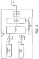
- a wireless transceiver 100 which includes a transmitter 102, a receiver 104, a transmitter power amplifier 106, a transmit/receive (TR) switch 110, and a filter section 112.
- the transceiver can also optionally include an RF coupler 114 which can be connected between filter section 112 and an antenna 116.
- the wireless transceiver will also include a switch controller 118 to control the operation of the T/R switch and any switching associated with filter section 112.
- the switch controller 118 can comprise any combination of analog or digital circuitry capable of carrying out the switch control functions described herein.
- a wireless transceiver in accordance with the inventive arrangements can have more or fewer components, but the wireless transceiver shown in FIG. 1 is sufficient to facilitate understanding of the invention.
- the transmitter 102 and receiver 104 can be designed to transmit and receive, respectively on one or more frequency bands of interest.
- the transmitter power amplifier 106 can be a conventional RF power amplifier which increases the power level of transmitted radio frequency (RF) signals produced by the transmitter 106 prior to such signals being communicating to the antenna 116.
- Low noise amplifier 108 can be a conventional high-performance amplifier with a relatively low noise figure that is designed to amplify relatively weak received signals coupled from the antenna 116.
- the transmitter power amplifier 106 is shown separately from the transmitter 102 in FIG. 1 , but those skilled in the art will appreciate that the transmitter power amplifier can also be considered as part of the transmitter 102.
- a receiver low noise amplifier 108 is shown as a separate component with respect to the receiver 104, but can be understood to be a part of the receiver circuitry 104.
- the T/R switch 110 is used to selectively control access to the antenna 116 as between the transmitter 102 and the receiver 104.
- the T/R switch must protect the sensitive components of the receiver low-noise amplifier 108 from the relatively high RF power levels output by the transmitter power amplifier 106. Accordingly, the T/R switch must provide a high degree of RF signal isolation as between the output of the transmitter power amplifier and the input of the receiver low noise-amplifier.
- Filter section 112 is coupled intermediate of the T/R switch 110 and RF coupler 114.
- the filter section advantageously includes a plurality of RF filters which are used for filtering RF signals which are received and transmitted.
- the RF filters can include a plurality of low-pass filters, each with a somewhat higher cutoff frequency to accommodate operations on different frequency bands. Different ones of the plurality of RF filters can be advantageously used when receiving and/or transmitting on different frequency bands of interest.
- a plurality of switches is advantageously included in the filter section 112 to facilitate selecting among the plurality of RF filters when operating on different frequency bands.
- RF coupler 114 is optionally provided in transceiver 100 to sample transmitted RF output signals before such signals are communicated to the antenna.
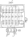
- FIG. 2 there is shown a conventional arrangement of a T/R switch and filter section as may be used in a wireless transceiver similar to wireless transceiver 100.
- the conventional T/R switch 210 is coupled to a transmitter power amplifier 206 and a receiver low-noise amplifier 208 as shown.
- a first switch 220a is used to selectively connect the power amplifier 206 to a common node 221 associated band switch network 223.
- a second switch 220b connects the common node 221 to the receiver low-noise amplifier 208. Accordingly, by selectively controlling the switches 220a, 220b using switch control signals, the T/R switch can control whether the common node 221 is connected to the transmitter power amplifier 206 or the receiver low noise amplifier 208.
- the band switch network 223 is comprised of a plurality of RF switches 222a-222f. Each of the RF switches is connected between the common node 221 of the band switching network and a first port of one of the plurality of RF filters 224a-224f. These harmonic filters are typically comprised of a plurality of low pass type filters, each with a progressively higher cutoff frequency to accommodate a transmitter frequency band of interest.
- a plurality of RF switches 226a-226f are connected between a common node 227 and a second port of one of the plurality of RF filters. Accordingly, the second band switch network 225 effectively controls which RF filter 224a-224f is connected to antenna port 216.
- an RF coupler is not shown in FIG. 2 but could be interposed between the common node 227 and the antenna port 216.
- the switching networks 223, 225 are provided so that the different harmonic filters can be switched into or out of the transmit path as needed for operation on a particular frequency band. Notably, these same output filters can often be used in receive mode as well.
- an antenna can be coupled to either the transmitter or receiver.
- Transmitted RF signals from the transmitter power amplifier 206 can be effectively routed through any RF filter 224a-224f before being communicated to the antenna port for transmission.
- received RF signals from the antenna port 216 can be routed through any of the RF filters 224a-224f before being communicated to the receiver low-noise amplifier 208.
- PIN diode based switches are commonly used to perform RF switching functions in a wireless transceiver. Moreover, to achieve a high level of RF signal isolation, PIN diode based switches in a series-shunt configuration are commonly used for this purpose. As such, pin diode based switches in series-shunt configuration are conventionally used to implement switches 220a, 220b, 222a-222f, and 226a-226f.
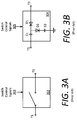
- FIG. 3A is a schematic drawing of a single pole single throw switch (SPST) switch 302, which is useful for representing the function of switches 220a, 220b, 222a-222f, and 226a-226f.
- SPST single pole single throw switch
- One or more switch control signals 303 can be applied to control the operation of the switch.
- FIG. 3B is a somewhat more detailed schematic diagram which shows a pin-diode type switch 304 having a series-shunt configuration as is commonly used to implement a SPST in a transceiver switching scenario as shown in FIGs. 1 and 2 .
- the switch 304 is comprised of a series diode D1 and a shunt diode D2 which are selectively biased to control the operation of the switch.
- Switch control signals 305 are used to control the selective bias voltage applied to the diodes.
- Capacitors C2 and C2 are used for blocking the DC bias voltages so that such bias voltages are not coupled to circuits external of the switch.
- the bias circuitry is not shown in FIG. 3B so as to avoid obscuring the invention.
- bias circuits for PIN diode switches as described herein are well known in the art, and any suitable bias circuit can be used for purposes of implementing the inventive arrangements.
- RF signals in switch 304 can be communicated from T1 to T2 with relatively low loss (e.g., typically 0.1 to 0.5 dB, depending on conditions of frequency, power level and so on) when the switch is in a low insertion loss state.
- relatively low loss e.g., typically 0.1 to 0.5 dB, depending on conditions of frequency, power level and so on
- D1 is forward biased and D2 is at zero or reverse bias.
- T1 is coupled or connected to T2.
- a high degree of RF signal isolation is obtained between T1 and T2 when D1 is at zero or reverse bias and D2 is forward biased.
- T1 is decoupled or disconnected from T2.
- the bias voltages applied to D1 and D2 are determined in accordance with the switch control signal(s) which control whether the switch is in a low insertion loss state as compared to a high isolation state.
- each switch 220a, 220b, 222a-222f, and 226a-226f will include one PIN diode (e.g. D1) which is disposed in series between the switched terminals T1 and T2.
- PIN diode e.g. D1
- Each such PIN diode in series will typically cause approximately 0.1 to 0.5 dB of signal loss (depending on frequency, power level and so on) when the switch is biased to the low insertion loss state and an RF signal is communicated between T1 to T2. Therefore, in a switching arrangement as shown in FIG.
- a relatively high insertion loss will result because there are always three (3) switches a signal must transit in the transmit path and in the receive path.
- RF filter 224d is required in a particular scenario, then transmitted RF signals will pass through RF switches 220a, 222d and 226d. The transmitted RF signal will transition one series PIN diode in each switch, for a total of three.
- FIG. 4 there is shown an improved arrangement for PIN diode T/R switching in a wireless transceiver, such as wireless transceiver 100.
- the arrangement is particularly valuable for use in handheld transceivers in which series-shunt PIN diode switches are used and battery life is an important design consideration.
- a filter section 412 includes a plurality of RF filters 424a-424f, each having a first port 427a 1 - 427f 1 and a second port and 427a 2 - 427f 2 .
- the harmonic filters are comprised of a plurality of low pass type filters, each with a progressively higher cutoff frequency to accommodate a different transmitter frequency band of interest.
- Switching networks are provided so that the different harmonic filters can be switched into or out of the transmit path as needed for operation on a particular frequency band.
- a first band switching network 423 is comprised of a first set of RF switches 422a-422f.
- Each of these RF switches is respectively connected between a first port of one of the plurality of RF filters 422a-422f and a common transmitter node or port 429 at which transmitter RF energy is received from a transmitter or power amplifier.
- the RF switches 422a-422f are responsive to one or more switch control signals 430 to selectively determine which RF filter is connected or coupled to the common transmitter port. Accordingly, the RF switches 422a-422f can selectively control or direct the transmitter RF energy so it exclusively applied to a first port of only one of the RF filters 424a-424f.
- the filter section also includes a second band switching network 425 comprised of a second group of RF switches 426a-426b.
- Each of these RF switches 426a-426b is respectively connected to the second port of one of the plurality of RF filters and to a common antenna port 416 at which RF energy is communicated to or from an antenna.
- the RF switches 426a-426f are responsive to one or more switch control signals 432 to selectively determine which RF filter is connected or coupled to the common antenna port. Accordingly, the RF switches 426a-426f can be controlled so that only one of the RF filters is coupled to the antenna port.
- a switch controller 418 can be used to control the RF switches 422a-422f and 426a-426f.
- the switch controller 418 can comprise any arrangement of circuitry capable of directly or indirectly biasing the PIN diodes switches for carrying out the switch operations described herein.
- a T/R switching network 410 is connected to the switching network 412 to facilitate transmit and receive switching.
- the T/R switching network is comprised of at least one receiver RF switch that is connected to at least one of the first ports 427a 1 -427f 1 , which is also defined herein as a T/R port.
- FIG. 4 shows that switch 420a and 420b are respectively connected to first ports 427c 1 and 427f 1 .
- Each switch 420a, 420b is also connected to a receiver port 434 at which received RF energy is communicated to a receiver.
- receiver port 434 can be connected or coupled to a low-noise amplifier 408 associated with a receiver (e.g. receiver 104).
- the one or more RF switches 420a, 420b associated with the T/R switching network are responsive to one or more control signals 436 to selectively control whether the switches are in the low insertion loss state, or high isolation state.
- the state of RF switches 420a, 420b determines whether received RF energy arriving at a first port of a particular RF filter (e.g. RF filter 420a or 420b) will be communicated to the input of the receiver.
- the switch control signals 430, 432 will respectively control each band switch network 423, 425 to determine the transmit path from transmitter port 429 to antenna port 416.
- RF filter 424d may be most suitable for controlling harmonic emissions.
- RF switches 422d and 426d can be controlled so as to be in their low-insertion loss (closed) state, thereby providing a low-insertion loss path through RF filter 424d. All other RF switches in band switch networks 423, 425 can be in the high isolation (open) state so as to restrict or prevent the flow of RF energy through the remaining RF filters.
- RF switches 420a, 420b are also in their high isolation (open) state so that high power RF signals from the transmitter port 429 cannot be communicated to the receiver port 434.
- RF filter 424a may be most suitable for controlling harmonic emissions. Accordingly, RF switches 422a and 426a can be controlled so as to be in their low-insertion loss (closed) state, thereby providing a low-insertion loss path through RF filter 424a. All other RF switches in band switch networks 423, 425 can be in the high isolation (open) state so as to restrict or prevent the flow of RF energy through the remaining RF filters. RF switches 420a, 420b remain in their high isolation (open) state so that high power RF signals from the transmitter port 429 cannot be communicated to the receiver port 434.
- band switch network 425 is used to route received RF signals from the antenna port 416 to a selected RF filter.
- band switch network 425 can be used to exclusively route received RF signals to any of the second ports 427a 2 - 427f 2 .
- the RF switches 420a, 420b in the T/R switching network are respectively connected to ports 427f 1 and 427c 1 and these ports are therefore also designated as T/R ports. Accordingly, the band switch network can exclusively route received RF signals to one of the T/R ports and received signals will be processed using RF filter 424c or 424f.
- RF switches 420a, 420b are used to control which of the T/R ports is connected to the receiver port 434.
- the switch controller 418 can be used to generate or coordinate switch control signals 436 to control the RF switches in the T/R switching network.
- each of the RF filters is a low pass filter, and each has a progressively higher cutoff frequency
- those RF filters with higher cutoff frequencies can often facilitate acceptable receive performance when used in place of RF filters with a lower cutoff frequency.
- RF filters 424a-424f are each low pass filters having progressively higher cutoff frequencies, with RF filter 424a having the lowest cutoff frequency and RF filter 424f having the highest cutoff frequency.
- RF filter 424f can pass all frequencies in the passband of RF filters 424a-424e since all such frequencies are lower than the cutoff frequency of RF filter 424f.
- RF filter 424f can in certain scenarios provide adequate filtering on all frequency bands. In that case, switch 420b would not be necessary and all receive signals would be instead routed through RF filter 424f and switch 420a.
- An advantage of this approach is that only one PIN diode switch (420a) is needed in the T/R switching network.
- an RF filter with a lower cutoff frequency for one or more operating bands of a multiband transceiver it may be desirable to use RF filter 424c when receiving signals associated with Bands 1, 2 and 3, and to use RF filter 424f when receiving signals associated with Bands 4, 5, and 6.
- This approach would require the use of two PIN diode switches (420a, 420b) in the T/R switching network 423, but offers better control of receiver filtering.
- the T/R switching network 410 can include one PIN diode switch for each RF filter. Each of these switches would be respectively connected between the receiver port 434 and one of the RF filters at ports 427a 2 -427f 1 .
- the receiver path in that scenario would be determined by the T/R switching network and the band switch network 425.
- switches 422a-422f can be set to their high isolation (open) state so that the receiver circuitry is isolated from the transmitter power amplifier 406.
- the inventive arrangements utilize existing PIN diode switches associated with the selection of transmitter harmonic filters (i.e., filters 424a-424f) to facilitate RF switching.
- the result is a reduced parts count since fewer RF switches are required.
- substantial power savings can be realized in a transceiver incorporating the inventive switching arrangements as described herein. Reducing the number of diodes in the transmit path from three to two will reduce power losses by an estimated 1.4 Watts of DC power. In a battery-powered handheld transceiver, the reduced power consumption during transmit can have a significant effect for purposes of extending battery life. Three series diodes will remain in the receive path, but this does not significantly affect transceiver performance.
Landscapes
- Engineering & Computer Science (AREA)
- Computer Networks & Wireless Communication (AREA)
- Signal Processing (AREA)
- Transceivers (AREA)
- Input Circuits Of Receivers And Coupling Of Receivers And Audio Equipment (AREA)
Abstract
Description
- The inventive arrangements relate to radio transceivers and more particularly to power saving switching configurations for multi-band transceivers that use multiple harmonic transmitter filters.
- A PIN diode is a diode with a wide, un-doped or lightly doped intrinsic semiconductor region that resides between a p-type semiconductor and an n-type semiconductor region. Under conditions where the PIN diode has zero bias or is reversed biased, it has a relatively low capacitance such that it presents a high insertion loss to a radio frequency (RF) signal. However, when the PIN diode is forward biased with sufficient current it will have only minimal resistance to RF signals (e.g. about 1 ohm). Due to these characteristics, PIN diodes are often used to form RF switches.
- One example switch configuration using PIN diodes comprises a series-shunt configuration. A series-shunt configuration PIN diode switch is conventionally used to achieve a relatively high isolation, which may be particularly important in high frequency applications, for example at or above 1 GHz. To achieve the relatively high isolation in a high power application, for example >10W, a relatively high reverse bias voltage is used. The series diode and shunt diode of a particular switched path must be forward and reversed biased complementarily to minimize insertion loss and maximize isolation.
- In transceivers, a transmit/receive (T/R) switch is often require to switch an antenna between the transmitter and receiver. However, switches (including PIN diode switches) are known to introduce insertion loss in the RF path. Such insertion loss will commonly range from 0.1 to 0.5 dB, depending on RF frequency, power levels, and so on.
- Embodiments of the invention concern a wireless transceiver which includes a plurality of RF filters, each having a first and second port. The transceiver includes a first band switching network comprised of a first plurality of RF switches, each respectively connected between the first port of one of the plurality of RF filters and a common transmitter port at which transmitter RF energy is received from a transmitter. The first plurality of RF switches is responsive to at least a first control signal to selectively direct the transmitter RF energy to a selected one of the RF filters. A second band switching network is comprised of a second plurality of RF switches, each respectively connected to the second port of one of the plurality of RF filters and coupled to a common antenna port at which RF energy is communicated to or from an antenna. The second band switching network is responsive to at least a second control signal which selectively controls which of the plurality of RF filters is connected to the common antenna port. The transceiver further includes a T/R switching network comprised of at least one receiver RF switch connected to at least one of the first ports, which is also a T/R port, and to a receiver port at which received RF energy is communicated to a receiver. The receiver RF switch is responsive to at least a third control signal to selectively permit the received RF energy arriving at the at least one T/R port to be communicated to the receiver. A switch control system controls at least the second band-switching network to selectively communicate received RF energy from the common antenna port to an active T/R port which is connected to the receiver port. Each of said first and second plurality of RF switches are PIN diodes switches having a PIN diode in series with a signal path. No more than two PIN diodes are present in the signal path between the common transmitter port and the common antenna port when any of the RF filters is in use.
- Embodiments will be described with reference to the following drawing figures, in which like numerals represent like items throughout the figures, and in which:
-
FIG. 1 is a block diagram or a radio transceiver that is useful for understanding the invention. -
FIG. 2 is a block diagram of a transceiver section showing a conventional switching arrangement for a plurality of harmonic filters. -
FIGs. 3A and 3B are drawing that are useful for understanding the operation of a PIN diode switch. -
FIG. 4 is a block diagram that is useful for understanding a transceiver section with a switching arrangement for a plurality of harmonic filters, in which only two series PIN diodes are required in the transmit path. - The invention is described with reference to the attached figures. The figures are not drawn to scale and they are provided merely to illustrate the instant invention. Several aspects of the invention are described below with reference to example applications for illustration. It should be understood that numerous specific details, relationships, and methods are set forth to provide a full understanding of the invention. One having ordinary skill in the relevant art, however, will readily recognize that the invention can be practiced without one or more of the specific details or with other methods. In other instances, well-known structures or operation are not shown in detail to avoid obscuring the invention. The invention is not limited by the illustrated ordering of acts or events, as some acts may occur in different orders and/or concurrently with other acts or events. Furthermore, not all illustrated acts or events are required to implement a methodology in accordance with the invention.
- Reference throughout this specification to "one embodiment", "an embodiment", or similar language means that a particular feature, structure, or characteristic described in connection with the indicated embodiment is included in at least one embodiment of the present invention. Thus, the phrases "in one embodiment", "in an embodiment", and similar language throughout this specification may, but do not necessarily, all refer to the same embodiment.
- In multi-band wireless transceivers, a plurality of harmonic filters are sometimes provided at the output of the transmitter to reduce harmonic emissions. These harmonic filters are typically comprised of a plurality of low pass type filters, each with a progressively higher cutoff frequency to accommodate a transmitter frequency band of interest. Switching circuits are typically provided so that the different harmonic filters can be switched into or out of the transmit path as needed for operation on a particular frequency band. Notably, these same output filters can often be used in receive mode as well.
- Referring now to
FIG. 1 , there is shown awireless transceiver 100, which includes atransmitter 102, areceiver 104, atransmitter power amplifier 106, a transmit/receive (TR)switch 110, and afilter section 112. The transceiver can also optionally include anRF coupler 114 which can be connected betweenfilter section 112 and anantenna 116. The wireless transceiver will also include aswitch controller 118 to control the operation of the T/R switch and any switching associated withfilter section 112. Theswitch controller 118 can comprise any combination of analog or digital circuitry capable of carrying out the switch control functions described herein. A wireless transceiver in accordance with the inventive arrangements can have more or fewer components, but the wireless transceiver shown inFIG. 1 is sufficient to facilitate understanding of the invention. - The
transmitter 102 andreceiver 104 can be designed to transmit and receive, respectively on one or more frequency bands of interest. Thetransmitter power amplifier 106 can be a conventional RF power amplifier which increases the power level of transmitted radio frequency (RF) signals produced by thetransmitter 106 prior to such signals being communicating to theantenna 116.Low noise amplifier 108 can be a conventional high-performance amplifier with a relatively low noise figure that is designed to amplify relatively weak received signals coupled from theantenna 116. For convenience, thetransmitter power amplifier 106 is shown separately from thetransmitter 102 inFIG. 1 , but those skilled in the art will appreciate that the transmitter power amplifier can also be considered as part of thetransmitter 102. Similarly, a receiverlow noise amplifier 108 is shown as a separate component with respect to thereceiver 104, but can be understood to be a part of thereceiver circuitry 104. - The T/
R switch 110 is used to selectively control access to theantenna 116 as between thetransmitter 102 and thereceiver 104. The T/R switch must protect the sensitive components of the receiver low-noise amplifier 108 from the relatively high RF power levels output by thetransmitter power amplifier 106. Accordingly, the T/R switch must provide a high degree of RF signal isolation as between the output of the transmitter power amplifier and the input of the receiver low noise-amplifier.Filter section 112 is coupled intermediate of the T/R switch 110 andRF coupler 114. The filter section advantageously includes a plurality of RF filters which are used for filtering RF signals which are received and transmitted. For example, in a multiband transceiver, the RF filters can include a plurality of low-pass filters, each with a somewhat higher cutoff frequency to accommodate operations on different frequency bands. Different ones of the plurality of RF filters can be advantageously used when receiving and/or transmitting on different frequency bands of interest. A plurality of switches is advantageously included in thefilter section 112 to facilitate selecting among the plurality of RF filters when operating on different frequency bands.RF coupler 114 is optionally provided intransceiver 100 to sample transmitted RF output signals before such signals are communicated to the antenna. - Referring now to
FIG. 2 , there is shown a conventional arrangement of a T/R switch and filter section as may be used in a wireless transceiver similar towireless transceiver 100. The conventional T/R switch 210 is coupled to atransmitter power amplifier 206 and a receiver low-noise amplifier 208 as shown. Afirst switch 220a is used to selectively connect thepower amplifier 206 to acommon node 221 associatedband switch network 223. Asecond switch 220b connects thecommon node 221 to the receiver low-noise amplifier 208. Accordingly, by selectively controlling theswitches common node 221 is connected to thetransmitter power amplifier 206 or the receiverlow noise amplifier 208. - The
band switch network 223 is comprised of a plurality ofRF switches 222a-222f. Each of the RF switches is connected between thecommon node 221 of the band switching network and a first port of one of the plurality ofRF filters 224a-224f. These harmonic filters are typically comprised of a plurality of low pass type filters, each with a progressively higher cutoff frequency to accommodate a transmitter frequency band of interest. In theband switch network 225, a plurality ofRF switches 226a-226f are connected between acommon node 227 and a second port of one of the plurality of RF filters. Accordingly, the secondband switch network 225 effectively controls which RF filter 224a-224f is connected toantenna port 216. Note that an RF coupler is not shown inFIG. 2 but could be interposed between thecommon node 227 and theantenna port 216.. The switchingnetworks - With the arrangement shown in
FIG. 2 , an antenna can be coupled to either the transmitter or receiver. Transmitted RF signals from thetransmitter power amplifier 206 can be effectively routed through anyRF filter 224a-224f before being communicated to the antenna port for transmission. Likewise, received RF signals from theantenna port 216 can be routed through any of theRF filters 224a-224f before being communicated to the receiver low-noise amplifier 208. - In order to facilitate fast switching time and high reliability, PIN diode based switches are commonly used to perform RF switching functions in a wireless transceiver. Moreover, to achieve a high level of RF signal isolation, PIN diode based switches in a series-shunt configuration are commonly used for this purpose. As such, pin diode based switches in series-shunt configuration are conventionally used to implement
switches -
FIG. 3A is a schematic drawing of a single pole single throw switch (SPST)switch 302, which is useful for representing the function ofswitches FIG. 3B is a somewhat more detailed schematic diagram which shows a pin-diode type switch 304 having a series-shunt configuration as is commonly used to implement a SPST in a transceiver switching scenario as shown inFIGs. 1 and2 . Theswitch 304 is comprised of a series diode D1 and a shunt diode D2 which are selectively biased to control the operation of the switch. Switch control signals 305 are used to control the selective bias voltage applied to the diodes. Capacitors C2 and C2 are used for blocking the DC bias voltages so that such bias voltages are not coupled to circuits external of the switch. The bias circuitry is not shown inFIG. 3B so as to avoid obscuring the invention. However, it will be appreciated that bias circuits for PIN diode switches as described herein are well known in the art, and any suitable bias circuit can be used for purposes of implementing the inventive arrangements. - The operation of pin-diode switches having a series-shunt configuration are well known and therefore will not be described here in detail. However, a brief explanation is provided for the convenience of the reader. In operation, RF signals in
switch 304 can be communicated from T1 to T2 with relatively low loss (e.g., typically 0.1 to 0.5 dB, depending on conditions of frequency, power level and so on) when the switch is in a low insertion loss state. In the low insertion loss state, D1 is forward biased and D2 is at zero or reverse bias. In this low insertion loss state, it can be said that T1 is coupled or connected to T2. Conversely, a high degree of RF signal isolation is obtained between T1 and T2 when D1 is at zero or reverse bias and D2 is forward biased. In this high isolation state, it can be said that T1 is decoupled or disconnected from T2. The bias voltages applied to D1 and D2 are determined in accordance with the switch control signal(s) which control whether the switch is in a low insertion loss state as compared to a high isolation state. - A PIN diode switching arrangement as shown and described herein with respect to
FIGs. 2 and3 can be effective but also suffers from certain drawbacks. As shown inFIG. 3 , eachswitch FIG. 2 , a relatively high insertion loss will result because there are always three (3) switches a signal must transit in the transmit path and in the receive path. For example, ifRF filter 224d is required in a particular scenario, then transmitted RF signals will pass throughRF switches - In the receive path, the presence of 0.1 to 0.5 dB of loss has relatively little impact on system performance. However, the same amount of loss in the transmit path can have a significant impact on battery life. Consider an exemplary scenario in which a
handheld transceiver 100 is specified to produce 5 watts of RF output and eachswitch - Referring now to
FIG. 4 , there is shown an improved arrangement for PIN diode T/R switching in a wireless transceiver, such aswireless transceiver 100. The arrangement is particularly valuable for use in handheld transceivers in which series-shunt PIN diode switches are used and battery life is an important design consideration. - As shown in
FIG. 4 , afilter section 412 includes a plurality ofRF filters 424a-424f, each having a first port 427a1 - 427f1 and a second port and 427a2 - 427f2. According to one aspect of the invention, the harmonic filters are comprised of a plurality of low pass type filters, each with a progressively higher cutoff frequency to accommodate a different transmitter frequency band of interest. Switching networks are provided so that the different harmonic filters can be switched into or out of the transmit path as needed for operation on a particular frequency band. For example, a firstband switching network 423 is comprised of a first set ofRF switches 422a-422f. Each of these RF switches is respectively connected between a first port of one of the plurality ofRF filters 422a-422f and a common transmitter node orport 429 at which transmitter RF energy is received from a transmitter or power amplifier. The RF switches 422a-422f are responsive to one or more switch control signals 430 to selectively determine which RF filter is connected or coupled to the common transmitter port. Accordingly, theRF switches 422a-422f can selectively control or direct the transmitter RF energy so it exclusively applied to a first port of only one of theRF filters 424a-424f. - The filter section also includes a second
band switching network 425 comprised of a second group ofRF switches 426a-426b. Each of theseRF switches 426a-426b is respectively connected to the second port of one of the plurality of RF filters and to acommon antenna port 416 at which RF energy is communicated to or from an antenna. The RF switches 426a-426f are responsive to one or more switch control signals 432 to selectively determine which RF filter is connected or coupled to the common antenna port. Accordingly, theRF switches 426a-426f can be controlled so that only one of the RF filters is coupled to the antenna port. Aswitch controller 418 can be used to control theRF switches 422a-422f and 426a-426f. Theswitch controller 418 can comprise any arrangement of circuitry capable of directly or indirectly biasing the PIN diodes switches for carrying out the switch operations described herein. - A T/
R switching network 410 is connected to theswitching network 412 to facilitate transmit and receive switching. The T/R switching network is comprised of at least one receiver RF switch that is connected to at least one of the first ports 427a1-427f1, which is also defined herein as a T/R port. For example,FIG. 4 shows that switch 420a and 420b are respectively connected to first ports 427c1 and 427f1. Eachswitch receiver port 434 at which received RF energy is communicated to a receiver. For example,receiver port 434 can be connected or coupled to a low-noise amplifier 408 associated with a receiver (e.g. receiver 104). The one ormore RF switches more control signals 436 to selectively control whether the switches are in the low insertion loss state, or high isolation state. As such, the state ofRF switches RF filter - The operation of the circuit in
FIG. 4 will now be described in greater detail. In transmit mode, the switch control signals 430, 432 will respectively control eachband switch network transmitter port 429 toantenna port 416. For example, when operating on a particular frequency band,RF filter 424d may be most suitable for controlling harmonic emissions. In such a scenario, RF switches 422d and 426d can be controlled so as to be in their low-insertion loss (closed) state, thereby providing a low-insertion loss path throughRF filter 424d. All other RF switches inband switch networks RF switches transmitter port 429 cannot be communicated to thereceiver port 434. When operating on a different frequency band,RF filter 424a may be most suitable for controlling harmonic emissions. Accordingly,RF switches RF filter 424a. All other RF switches inband switch networks RF switches transmitter port 429 cannot be communicated to thereceiver port 434. - Notably, in the embodiment shown in
FIG. 4 , only two PIN diode switches are present in the transmit path, regardless of which RF filter is selected. For example, ifRF filter 424d is in use, then onlyRF switches FIG. 2 , where three PIN diode switches are always present in the transmit path. - When operating conditions require a transition to receive mode,
band switch network 425 is used to route received RF signals from theantenna port 416 to a selected RF filter. For example,band switch network 425 can be used to exclusively route received RF signals to any of the second ports 427a2 - 427f2. InFIG. 4 , theRF switches RF filter RF switches receiver port 434. Theswitch controller 418 can be used to generate or coordinate switch control signals 436 to control the RF switches in the T/R switching network. - In an embodiment of the invention where each of the RF filters is a low pass filter, and each has a progressively higher cutoff frequency, those RF filters with higher cutoff frequencies can often facilitate acceptable receive performance when used in place of RF filters with a lower cutoff frequency. For example, assume that
RF filters 424a-424f are each low pass filters having progressively higher cutoff frequencies, withRF filter 424a having the lowest cutoff frequency andRF filter 424f having the highest cutoff frequency. In such a scenario,RF filter 424f can pass all frequencies in the passband ofRF filters 424a-424e since all such frequencies are lower than the cutoff frequency ofRF filter 424f. Accordingly, for receive operation;RF filter 424f can in certain scenarios provide adequate filtering on all frequency bands. In that case,switch 420b would not be necessary and all receive signals would be instead routed throughRF filter 424f and switch 420a. An advantage of this approach is that only one PIN diode switch (420a) is needed in the T/R switching network. - In other receiving scenarios, it may be desirable to use an RF filter with a lower cutoff frequency for one or more operating bands of a multiband transceiver. For example, it may be desirable to use
RF filter 424c when receiving signals associated withBands RF filter 424f when receiving signals associated withBands R switching network 423, but offers better control of receiver filtering. - According to another scenario, it may be desirable to use a different specific one of the
RF filters 424a-424f for receiver operations when performing receive operations on each transceiver band. In that case, instead of just twoRF switches R switching network 410 can include one PIN diode switch for each RF filter. Each of these switches would be respectively connected between thereceiver port 434 and one of the RF filters at ports 427a2 -427f1. The receiver path in that scenario would be determined by the T/R switching network and theband switch network 425. In each of the foregoing scenarios,switches 422a-422f can be set to their high isolation (open) state so that the receiver circuitry is isolated from thetransmitter power amplifier 406. - The inventive arrangements utilize existing PIN diode switches associated with the selection of transmitter harmonic filters (i.e.,
filters 424a-424f) to facilitate RF switching. The result is a reduced parts count since fewer RF switches are required. Moreover, substantial power savings can be realized in a transceiver incorporating the inventive switching arrangements as described herein. Reducing the number of diodes in the transmit path from three to two will reduce power losses by an estimated 1.4 Watts of DC power. In a battery-powered handheld transceiver, the reduced power consumption during transmit can have a significant effect for purposes of extending battery life. Three series diodes will remain in the receive path, but this does not significantly affect transceiver performance. - The terminology used herein is for the purpose of describing particular embodiments only and is not intended to be limiting of the invention. As used herein, the singular forms "a", "an" and "the" are intended to include the plural forms as well, unless the context clearly indicates otherwise. Furthermore, to the extent that the terms "including", "includes", "having", "has", "with", or variants thereof are used in either the detailed description and/or the claims, such terms are intended to be inclusive in a manner similar to the term "comprising."
- Unless otherwise defined, all terms (including technical and scientific terms) used herein have the same meaning as commonly understood by one of ordinary skill in the art to which this invention belongs. It will be further understood that terms, such as those defined in commonly used dictionaries, should be interpreted as having a meaning that is consistent with their meaning in the context of the relevant art and will not be interpreted in an idealized or overly formal sense unless expressly so defined herein.
- Although the invention has been illustrated and described with respect to one or more implementations, equivalent alterations and modifications will occur to others skilled in the art upon the reading and understanding of this specification and the annexed drawings. In addition, while a particular feature of the invention may have been disclosed with respect to only one of several implementations, such feature may be combined with one or more other features of the other implementations as may be desired and advantageous for any given or particular application. Thus, the breadth and scope of the present invention should not be limited by any of the above described embodiments. Rather, the scope of the invention should be defined in accordance with the following claims and their equivalents.
Claims (10)
- A wireless transceiver, comprising:a plurality of RF filters, each having a first and second port;a first band switching network comprised of a first plurality of RF switches, each respectively connected between the first port of one of the plurality of RF filters and a common transmitter port at which transmitter RF energy is received from a transmitter, the first plurality of RF switches responsive to at least a first control signal to selectively direct said transmitter RF energy to a selected one of the RF filters;a second band switching network comprised of a second plurality of RF switches, each respectively connected to the second port of one of the plurality of RF filters and coupled to a common antenna port at which RF energy is communicated to or from an antennaa T/R switching network comprised of at least one receiver RF switch connected to at least one of the first ports, which is also a T/R port, and to a receiver port at which received RF energy is communicated to a receiver, the at least one receiver RF switch responsive to at least a second control signal to selectively permit the received RF energy arriving at the T/R port to be communicated to the receiver.
- The wireless transceiver according to claim 1, wherein only two series diodes are present in each transmit path defined in the wireless transceiver from the common transmitter port to the common antenna port when any of the RF filters is in use.
- A wireless transceiver, comprising:a plurality of RF filters, each having a first and second port;a first band switching network comprised of a first plurality of RF switches, each respectively connected between the first port of one of the plurality of RF filters and a common transmitter port at which transmitter RF energy is received from a transmitter, the first plurality of RF switches responsive to at least a first control signal to selectively direct said transmitter RF energy to a selected one of the RF filters;a second band switching network comprised of a second plurality of RF switches, each respectively connected to the second port of one of the plurality of RF filters and coupled to a common antenna port at which RF energy is communicated to or from an antenna, the second band switching network responsive to at least a second control signal which selectively controls which of the plurality of RF filters is connected to the common antenna port;a T/R switching network comprised of at least one receiver RF switch connected to at least one of the first ports, which is also a T/R port, and to a receiver port at which received RF energy is communicated to a receiver, the at least one receiver RF switch responsive to at least a third control signal to selectively permit the received RF energy arriving at the at least one T/R port to be communicated to the receiver; anda switch control system which controls the second band-switching network to selectively communicate received RF energy from the common antenna port to an active T/R port which is connected to the receiver port;wherein each of said first and second plurality of RF switches are PIN diodes switches having a PIN diode in series with a signal path, whereby no more than two PIN diodes are present in the signal path between the common transmitter port and the common antenna port when any of the RF filters is in use.
- The wireless transceiver according to claim 3, wherein the at least one receiver RF switch is a PIN diode switch.
- The wireless transceiver according to claim 3, wherein the at least one receiver RF switch is a PIN diode switch having PIN diodes arranged in a series-shunt configuration.
- The wireless transceiver according to claim 3, wherein the T/R switching network includes a plurality of the receiver RF switches respectively connected to a plurality of the first ports which are T/R ports, and to the receiver port at which the received RF energy is communicated to the receiver.
- A wireless transceiver, comprising:a plurality of RF filters, each having a first and second port;a first band switching network comprised of a first plurality of RF switches, each respectively connected between the first port of one of the plurality of RF filters and a common transmitter port at which transmitter RF energy is received from a transmitter, the first plurality of RF switches responsive to at least a first control signal to selectively direct said transmitter RF energy to a selected one of the RF filters;a T/R switching network comprised of at least one receiver RF switch connected to at least one of the first ports, which is also a T/R port, and to a receiver port at which received RF energy is communicated to a receiver, the at least one receiver RF switch responsive to at least a second control signal to selectively permit the received RF energy arriving at the T/R port to be communicated to the receiver;a second band switching network responsive to at least a third control signal to selectively communicate received RF energy from a common antenna port, through one of the plurality of RF filters, to the T/R port which is active when the T/R switching network causes the received RF energy arriving at the T/R port that is active to be communicated to the receiver;wherein only two series PIN diodes are present in each transmit path defined in the wireless transceiver from the common transmitter port to the common antenna port when any of the RF filters is in use.
- The wireless transceiver according to claim 7, wherein each of the first plurality of RF switches and the at least one receiver RF switch is a PIN diode switch.
- The wireless transceiver according to claim 7, wherein the at least one receiver RF switch is a PIN diode switch having PIN diodes arranged in a series-shunt configuration.
- The wireless transceiver according to claim 7, wherein the plurality of RF filters are low-pass filters, each defining a low pass filter band with a different cut-off frequency and only one T/R port is provided, wherein the RF filter which is associated with the one T/R port is the RF filter that has the highest cut-off frequency of any of the plurality of RF filters.
Applications Claiming Priority (1)
| Application Number | Priority Date | Filing Date | Title |
|---|---|---|---|
| US14/620,296 US9961631B2 (en) | 2015-02-12 | 2015-02-12 | Power saving transceiver switch configuration |
Publications (3)
| Publication Number | Publication Date |
|---|---|
| EP3057230A2 true EP3057230A2 (en) | 2016-08-17 |
| EP3057230A3 EP3057230A3 (en) | 2016-10-12 |
| EP3057230B1 EP3057230B1 (en) | 2019-10-30 |
Family
ID=55129510
Family Applications (1)
| Application Number | Title | Priority Date | Filing Date |
|---|---|---|---|
| EP16000040.2A Active EP3057230B1 (en) | 2015-02-12 | 2016-01-11 | Power saving transceiver switch configuration |
Country Status (2)
| Country | Link |
|---|---|
| US (1) | US9961631B2 (en) |
| EP (1) | EP3057230B1 (en) |
Families Citing this family (9)
| Publication number | Priority date | Publication date | Assignee | Title |
|---|---|---|---|---|
| US10320043B2 (en) * | 2017-05-23 | 2019-06-11 | Nanning Fugui Precision Industrial Co., Ltd. | Power distributing device |
| US10361745B2 (en) | 2017-06-28 | 2019-07-23 | Qualcomm Incorporated | Systems and methods for reducing transmit and receive power via a T/R switch |
| EP3685467B1 (en) * | 2017-09-22 | 2021-07-07 | Telefonaktiebolaget LM Ericsson (PUBL) | Antenna connection circuits |
| JP2020170919A (en) * | 2019-04-02 | 2020-10-15 | 株式会社村田製作所 | High frequency signal transmission/reception circuit |
| US11380968B2 (en) * | 2019-10-31 | 2022-07-05 | Skyworks Solutions, Inc. | DC bias configuration for pin diode SPDT switch |
| CN115398810B (en) * | 2020-04-24 | 2024-08-20 | 株式会社村田制作所 | High-frequency module and communication device |
| US12052049B2 (en) | 2021-07-08 | 2024-07-30 | Macom Technology Solutions Holdings, Inc. | TR switch with high RX power protection |
| IL288247B2 (en) * | 2021-11-19 | 2024-01-01 | D Fend Solutions Ad Ltd | A self-controlled microwave filtration system |
| CN114584119B (en) * | 2022-03-04 | 2022-10-11 | 扬州万方科技股份有限公司 | Wireless communication system receiving and transmitting switch circuit with power-off protection |
Family Cites Families (5)
| Publication number | Priority date | Publication date | Assignee | Title |
|---|---|---|---|---|
| US8680947B1 (en) | 2009-07-24 | 2014-03-25 | Rf Micro Devices, Inc. | Passive multi-band duplexer |
| DE102010046677B4 (en) | 2010-09-27 | 2017-10-12 | Snaptrack Inc. | circuitry |
| DE102011101756B4 (en) * | 2011-05-17 | 2018-03-22 | Snaptrack, Inc. | Surface acoustic wave filter device |
| US9030270B2 (en) * | 2012-08-03 | 2015-05-12 | Entropic Communications, Inc. | Cascaded diplexer circuit |
| US9515645B2 (en) * | 2014-06-03 | 2016-12-06 | Infineon Technologies Ag | System and method for a radio frequency switch |
-
2015
- 2015-02-12 US US14/620,296 patent/US9961631B2/en active Active
-
2016
- 2016-01-11 EP EP16000040.2A patent/EP3057230B1/en active Active
Non-Patent Citations (1)
| Title |
|---|
| None |
Also Published As
| Publication number | Publication date |
|---|---|
| US20160242113A1 (en) | 2016-08-18 |
| EP3057230A3 (en) | 2016-10-12 |
| EP3057230B1 (en) | 2019-10-30 |
| US9961631B2 (en) | 2018-05-01 |
Similar Documents
| Publication | Publication Date | Title |
|---|---|---|
| EP3057230A2 (en) | Power saving transceiver switch configuration | |
| US10389310B2 (en) | Radio-frequency signal amplifier circuit, power amplifier module, front-end circuit, and communication device | |
| US8253485B2 (en) | Power amplifier | |
| CN105049015B (en) | The single-pole double throw RF switch and hilted broadsword of single-pole single-throw(SPST RF switch and its composition throw RF switch more | |
| KR101428003B1 (en) | RF Switch with Transformer and Switching Method thereof | |
| US10153803B2 (en) | Receiving circuit, wireless communication module, and wireless communication device | |
| US10778211B2 (en) | Switching circuit and semiconductor module | |
| US20140306780A1 (en) | Duplexers | |
| CN109150227B (en) | Multi-mode radio frequency front-end circuit and control method thereof | |
| US20140009208A1 (en) | CMOS Switching Circuitry of a Transmitter Module | |
| CN106571850A (en) | Bidirectional amplifier of TDD mode | |
| CN111211805A (en) | Balanced radio frequency front end receiving and transmitting circuit, system and control method thereof | |
| CN210780780U (en) | Balanced RF front-end transceiver circuit and system | |
| US20220006483A1 (en) | Transmit/receive switch circuits for time division duplex communications systems | |
| US20190229415A1 (en) | Radio-Frequency Apparatus with Integrated Antenna Control and Associated Methods | |
| KR20180124578A (en) | SPDT switch structure including Transmission Line Transformer(TLT) for single antenna operation | |
| US9413415B2 (en) | High frequency module | |
| CN210297678U (en) | UHF frequency channel airborne transmitting radio frequency circuit | |
| CN113541709A (en) | Front End Modules and RF Modules | |
| WO2020129882A1 (en) | Front end module and communication device | |
| KR102408077B1 (en) | High-frequency modules and communication devices | |
| US6856187B2 (en) | High frequency switch module | |
| KR100613580B1 (en) | Dual antenna unit with improved separation | |
| US20240195366A1 (en) | Amplifier circuit and radio-frequency circuit | |
| KR101901699B1 (en) | Antenna switch circuit with improved harmonic suppression characteristic |
Legal Events
| Date | Code | Title | Description |
|---|---|---|---|
| PUAI | Public reference made under article 153(3) epc to a published international application that has entered the european phase |
Free format text: ORIGINAL CODE: 0009012 |
|
| 17P | Request for examination filed |
Effective date: 20160111 |
|
| AK | Designated contracting states |
Kind code of ref document: A2 Designated state(s): AL AT BE BG CH CY CZ DE DK EE ES FI FR GB GR HR HU IE IS IT LI LT LU LV MC MK MT NL NO PL PT RO RS SE SI SK SM TR |
|
| AX | Request for extension of the european patent |
Extension state: BA ME |
|
| PUAL | Search report despatched |
Free format text: ORIGINAL CODE: 0009013 |
|
| AK | Designated contracting states |
Kind code of ref document: A3 Designated state(s): AL AT BE BG CH CY CZ DE DK EE ES FI FR GB GR HR HU IE IS IT LI LT LU LV MC MK MT NL NO PL PT RO RS SE SI SK SM TR |
|
| AX | Request for extension of the european patent |
Extension state: BA ME |
|
| RIC1 | Information provided on ipc code assigned before grant |
Ipc: H04W 52/02 20090101ALI20160905BHEP Ipc: H03H 7/46 20060101AFI20160905BHEP |
|
| STAA | Information on the status of an ep patent application or granted ep patent |
Free format text: STATUS: EXAMINATION IS IN PROGRESS |
|
| 17Q | First examination report despatched |
Effective date: 20180112 |
|
| RAP1 | Party data changed (applicant data changed or rights of an application transferred) |
Owner name: HARRIS GLOBAL COMMUNICATIONS, INC. |
|
| GRAP | Despatch of communication of intention to grant a patent |
Free format text: ORIGINAL CODE: EPIDOSNIGR1 |
|
| STAA | Information on the status of an ep patent application or granted ep patent |
Free format text: STATUS: GRANT OF PATENT IS INTENDED |
|
| INTG | Intention to grant announced |
Effective date: 20190604 |
|
| GRAS | Grant fee paid |
Free format text: ORIGINAL CODE: EPIDOSNIGR3 |
|
| GRAA | (expected) grant |
Free format text: ORIGINAL CODE: 0009210 |
|
| STAA | Information on the status of an ep patent application or granted ep patent |
Free format text: STATUS: THE PATENT HAS BEEN GRANTED |
|
| AK | Designated contracting states |
Kind code of ref document: B1 Designated state(s): AL AT BE BG CH CY CZ DE DK EE ES FI FR GB GR HR HU IE IS IT LI LT LU LV MC MK MT NL NO PL PT RO RS SE SI SK SM TR |
|
| REG | Reference to a national code |
Ref country code: GB Ref legal event code: FG4D |
|
| REG | Reference to a national code |
Ref country code: CH Ref legal event code: EP |
|
| REG | Reference to a national code |
Ref country code: AT Ref legal event code: REF Ref document number: 1197237 Country of ref document: AT Kind code of ref document: T Effective date: 20191115 |
|
| REG | Reference to a national code |
Ref country code: DE Ref legal event code: R096 Ref document number: 602016023154 Country of ref document: DE |
|
| REG | Reference to a national code |
Ref country code: IE Ref legal event code: FG4D |
|
| REG | Reference to a national code |
Ref country code: LT Ref legal event code: MG4D |
|
| PG25 | Lapsed in a contracting state [announced via postgrant information from national office to epo] |
Ref country code: LV Free format text: LAPSE BECAUSE OF FAILURE TO SUBMIT A TRANSLATION OF THE DESCRIPTION OR TO PAY THE FEE WITHIN THE PRESCRIBED TIME-LIMIT Effective date: 20191030 Ref country code: SE Free format text: LAPSE BECAUSE OF FAILURE TO SUBMIT A TRANSLATION OF THE DESCRIPTION OR TO PAY THE FEE WITHIN THE PRESCRIBED TIME-LIMIT Effective date: 20191030 Ref country code: PL Free format text: LAPSE BECAUSE OF FAILURE TO SUBMIT A TRANSLATION OF THE DESCRIPTION OR TO PAY THE FEE WITHIN THE PRESCRIBED TIME-LIMIT Effective date: 20191030 Ref country code: NO Free format text: LAPSE BECAUSE OF FAILURE TO SUBMIT A TRANSLATION OF THE DESCRIPTION OR TO PAY THE FEE WITHIN THE PRESCRIBED TIME-LIMIT Effective date: 20200130 Ref country code: BG Free format text: LAPSE BECAUSE OF FAILURE TO SUBMIT A TRANSLATION OF THE DESCRIPTION OR TO PAY THE FEE WITHIN THE PRESCRIBED TIME-LIMIT Effective date: 20200130 Ref country code: GR Free format text: LAPSE BECAUSE OF FAILURE TO SUBMIT A TRANSLATION OF THE DESCRIPTION OR TO PAY THE FEE WITHIN THE PRESCRIBED TIME-LIMIT Effective date: 20200131 Ref country code: LT Free format text: LAPSE BECAUSE OF FAILURE TO SUBMIT A TRANSLATION OF THE DESCRIPTION OR TO PAY THE FEE WITHIN THE PRESCRIBED TIME-LIMIT Effective date: 20191030 Ref country code: FI Free format text: LAPSE BECAUSE OF FAILURE TO SUBMIT A TRANSLATION OF THE DESCRIPTION OR TO PAY THE FEE WITHIN THE PRESCRIBED TIME-LIMIT Effective date: 20191030 Ref country code: NL Free format text: LAPSE BECAUSE OF FAILURE TO SUBMIT A TRANSLATION OF THE DESCRIPTION OR TO PAY THE FEE WITHIN THE PRESCRIBED TIME-LIMIT Effective date: 20191030 Ref country code: PT Free format text: LAPSE BECAUSE OF FAILURE TO SUBMIT A TRANSLATION OF THE DESCRIPTION OR TO PAY THE FEE WITHIN THE PRESCRIBED TIME-LIMIT Effective date: 20200302 |
|
| REG | Reference to a national code |
Ref country code: NL Ref legal event code: MP Effective date: 20191030 |
|
| PG25 | Lapsed in a contracting state [announced via postgrant information from national office to epo] |
Ref country code: HR Free format text: LAPSE BECAUSE OF FAILURE TO SUBMIT A TRANSLATION OF THE DESCRIPTION OR TO PAY THE FEE WITHIN THE PRESCRIBED TIME-LIMIT Effective date: 20191030 Ref country code: RS Free format text: LAPSE BECAUSE OF FAILURE TO SUBMIT A TRANSLATION OF THE DESCRIPTION OR TO PAY THE FEE WITHIN THE PRESCRIBED TIME-LIMIT Effective date: 20191030 Ref country code: IS Free format text: LAPSE BECAUSE OF FAILURE TO SUBMIT A TRANSLATION OF THE DESCRIPTION OR TO PAY THE FEE WITHIN THE PRESCRIBED TIME-LIMIT Effective date: 20200229 |
|
| PG25 | Lapsed in a contracting state [announced via postgrant information from national office to epo] |
Ref country code: AL Free format text: LAPSE BECAUSE OF FAILURE TO SUBMIT A TRANSLATION OF THE DESCRIPTION OR TO PAY THE FEE WITHIN THE PRESCRIBED TIME-LIMIT Effective date: 20191030 |
|
| PG25 | Lapsed in a contracting state [announced via postgrant information from national office to epo] |
Ref country code: RO Free format text: LAPSE BECAUSE OF FAILURE TO SUBMIT A TRANSLATION OF THE DESCRIPTION OR TO PAY THE FEE WITHIN THE PRESCRIBED TIME-LIMIT Effective date: 20191030 Ref country code: EE Free format text: LAPSE BECAUSE OF FAILURE TO SUBMIT A TRANSLATION OF THE DESCRIPTION OR TO PAY THE FEE WITHIN THE PRESCRIBED TIME-LIMIT Effective date: 20191030 Ref country code: DK Free format text: LAPSE BECAUSE OF FAILURE TO SUBMIT A TRANSLATION OF THE DESCRIPTION OR TO PAY THE FEE WITHIN THE PRESCRIBED TIME-LIMIT Effective date: 20191030 Ref country code: ES Free format text: LAPSE BECAUSE OF FAILURE TO SUBMIT A TRANSLATION OF THE DESCRIPTION OR TO PAY THE FEE WITHIN THE PRESCRIBED TIME-LIMIT Effective date: 20191030 Ref country code: CZ Free format text: LAPSE BECAUSE OF FAILURE TO SUBMIT A TRANSLATION OF THE DESCRIPTION OR TO PAY THE FEE WITHIN THE PRESCRIBED TIME-LIMIT Effective date: 20191030 |
|
| REG | Reference to a national code |
Ref country code: DE Ref legal event code: R097 Ref document number: 602016023154 Country of ref document: DE |
|
| REG | Reference to a national code |
Ref country code: AT Ref legal event code: MK05 Ref document number: 1197237 Country of ref document: AT Kind code of ref document: T Effective date: 20191030 |
|
| PG25 | Lapsed in a contracting state [announced via postgrant information from national office to epo] |
Ref country code: SM Free format text: LAPSE BECAUSE OF FAILURE TO SUBMIT A TRANSLATION OF THE DESCRIPTION OR TO PAY THE FEE WITHIN THE PRESCRIBED TIME-LIMIT Effective date: 20191030 Ref country code: SK Free format text: LAPSE BECAUSE OF FAILURE TO SUBMIT A TRANSLATION OF THE DESCRIPTION OR TO PAY THE FEE WITHIN THE PRESCRIBED TIME-LIMIT Effective date: 20191030 Ref country code: MC Free format text: LAPSE BECAUSE OF FAILURE TO SUBMIT A TRANSLATION OF THE DESCRIPTION OR TO PAY THE FEE WITHIN THE PRESCRIBED TIME-LIMIT Effective date: 20191030 |
|
| REG | Reference to a national code |
Ref country code: CH Ref legal event code: PL |
|
| PLBE | No opposition filed within time limit |
Free format text: ORIGINAL CODE: 0009261 |
|
| STAA | Information on the status of an ep patent application or granted ep patent |
Free format text: STATUS: NO OPPOSITION FILED WITHIN TIME LIMIT |
|
| 26N | No opposition filed |
Effective date: 20200731 |
|
| REG | Reference to a national code |
Ref country code: BE Ref legal event code: MM Effective date: 20200131 |
|
| PG25 | Lapsed in a contracting state [announced via postgrant information from national office to epo] |
Ref country code: LU Free format text: LAPSE BECAUSE OF NON-PAYMENT OF DUE FEES Effective date: 20200111 |
|
| PG25 | Lapsed in a contracting state [announced via postgrant information from national office to epo] |
Ref country code: SI Free format text: LAPSE BECAUSE OF FAILURE TO SUBMIT A TRANSLATION OF THE DESCRIPTION OR TO PAY THE FEE WITHIN THE PRESCRIBED TIME-LIMIT Effective date: 20191030 Ref country code: LI Free format text: LAPSE BECAUSE OF NON-PAYMENT OF DUE FEES Effective date: 20200131 Ref country code: CH Free format text: LAPSE BECAUSE OF NON-PAYMENT OF DUE FEES Effective date: 20200131 Ref country code: AT Free format text: LAPSE BECAUSE OF FAILURE TO SUBMIT A TRANSLATION OF THE DESCRIPTION OR TO PAY THE FEE WITHIN THE PRESCRIBED TIME-LIMIT Effective date: 20191030 Ref country code: BE Free format text: LAPSE BECAUSE OF NON-PAYMENT OF DUE FEES Effective date: 20200131 |
|
| PG25 | Lapsed in a contracting state [announced via postgrant information from national office to epo] |
Ref country code: IE Free format text: LAPSE BECAUSE OF NON-PAYMENT OF DUE FEES Effective date: 20200111 |
|
| PG25 | Lapsed in a contracting state [announced via postgrant information from national office to epo] |
Ref country code: TR Free format text: LAPSE BECAUSE OF FAILURE TO SUBMIT A TRANSLATION OF THE DESCRIPTION OR TO PAY THE FEE WITHIN THE PRESCRIBED TIME-LIMIT Effective date: 20191030 Ref country code: MT Free format text: LAPSE BECAUSE OF FAILURE TO SUBMIT A TRANSLATION OF THE DESCRIPTION OR TO PAY THE FEE WITHIN THE PRESCRIBED TIME-LIMIT Effective date: 20191030 Ref country code: CY Free format text: LAPSE BECAUSE OF FAILURE TO SUBMIT A TRANSLATION OF THE DESCRIPTION OR TO PAY THE FEE WITHIN THE PRESCRIBED TIME-LIMIT Effective date: 20191030 |
|
| PG25 | Lapsed in a contracting state [announced via postgrant information from national office to epo] |
Ref country code: MK Free format text: LAPSE BECAUSE OF FAILURE TO SUBMIT A TRANSLATION OF THE DESCRIPTION OR TO PAY THE FEE WITHIN THE PRESCRIBED TIME-LIMIT Effective date: 20191030 |
|
| P01 | Opt-out of the competence of the unified patent court (upc) registered |
Effective date: 20230530 |
|
| PGFP | Annual fee paid to national office [announced via postgrant information from national office to epo] |
Ref country code: DE Payment date: 20250129 Year of fee payment: 10 |
|
| PGFP | Annual fee paid to national office [announced via postgrant information from national office to epo] |
Ref country code: FR Payment date: 20250127 Year of fee payment: 10 |
|
| PGFP | Annual fee paid to national office [announced via postgrant information from national office to epo] |
Ref country code: GB Payment date: 20250127 Year of fee payment: 10 Ref country code: IT Payment date: 20250121 Year of fee payment: 10 |