EP3054573A1 - Methods and systems for improving load transient response in power conversion systems - Google Patents
Methods and systems for improving load transient response in power conversion systems Download PDFInfo
- Publication number
- EP3054573A1 EP3054573A1 EP16153117.3A EP16153117A EP3054573A1 EP 3054573 A1 EP3054573 A1 EP 3054573A1 EP 16153117 A EP16153117 A EP 16153117A EP 3054573 A1 EP3054573 A1 EP 3054573A1
- Authority
- EP
- European Patent Office
- Prior art keywords
- converter
- primary stage
- primary
- stage
- load
- Prior art date
- Legal status (The legal status is an assumption and is not a legal conclusion. Google has not performed a legal analysis and makes no representation as to the accuracy of the status listed.)
- Granted
Links
Images

Classifications
-
- H—ELECTRICITY
- H02—GENERATION; CONVERSION OR DISTRIBUTION OF ELECTRIC POWER
- H02M—APPARATUS FOR CONVERSION BETWEEN AC AND AC, BETWEEN AC AND DC, OR BETWEEN DC AND DC, AND FOR USE WITH MAINS OR SIMILAR POWER SUPPLY SYSTEMS; CONVERSION OF DC OR AC INPUT POWER INTO SURGE OUTPUT POWER; CONTROL OR REGULATION THEREOF
- H02M1/00—Details of apparatus for conversion
- H02M1/42—Circuits or arrangements for compensating for or adjusting power factor in converters or inverters
- H02M1/4208—Arrangements for improving power factor of AC input
- H02M1/4225—Arrangements for improving power factor of AC input using a non-isolated boost converter
-
- H—ELECTRICITY
- H02—GENERATION; CONVERSION OR DISTRIBUTION OF ELECTRIC POWER
- H02M—APPARATUS FOR CONVERSION BETWEEN AC AND AC, BETWEEN AC AND DC, OR BETWEEN DC AND DC, AND FOR USE WITH MAINS OR SIMILAR POWER SUPPLY SYSTEMS; CONVERSION OF DC OR AC INPUT POWER INTO SURGE OUTPUT POWER; CONTROL OR REGULATION THEREOF
- H02M1/00—Details of apparatus for conversion
- H02M1/14—Arrangements for reducing ripples from DC input or output
-
- H—ELECTRICITY
- H02—GENERATION; CONVERSION OR DISTRIBUTION OF ELECTRIC POWER
- H02M—APPARATUS FOR CONVERSION BETWEEN AC AND AC, BETWEEN AC AND DC, OR BETWEEN DC AND DC, AND FOR USE WITH MAINS OR SIMILAR POWER SUPPLY SYSTEMS; CONVERSION OF DC OR AC INPUT POWER INTO SURGE OUTPUT POWER; CONTROL OR REGULATION THEREOF
- H02M1/00—Details of apparatus for conversion
- H02M1/42—Circuits or arrangements for compensating for or adjusting power factor in converters or inverters
-
- H—ELECTRICITY
- H02—GENERATION; CONVERSION OR DISTRIBUTION OF ELECTRIC POWER
- H02M—APPARATUS FOR CONVERSION BETWEEN AC AND AC, BETWEEN AC AND DC, OR BETWEEN DC AND DC, AND FOR USE WITH MAINS OR SIMILAR POWER SUPPLY SYSTEMS; CONVERSION OF DC OR AC INPUT POWER INTO SURGE OUTPUT POWER; CONTROL OR REGULATION THEREOF
- H02M3/00—Conversion of DC power input into DC power output
- H02M3/02—Conversion of DC power input into DC power output without intermediate conversion into AC
- H02M3/04—Conversion of DC power input into DC power output without intermediate conversion into AC by static converters
-
- H—ELECTRICITY
- H02—GENERATION; CONVERSION OR DISTRIBUTION OF ELECTRIC POWER
- H02M—APPARATUS FOR CONVERSION BETWEEN AC AND AC, BETWEEN AC AND DC, OR BETWEEN DC AND DC, AND FOR USE WITH MAINS OR SIMILAR POWER SUPPLY SYSTEMS; CONVERSION OF DC OR AC INPUT POWER INTO SURGE OUTPUT POWER; CONTROL OR REGULATION THEREOF
- H02M3/00—Conversion of DC power input into DC power output
- H02M3/02—Conversion of DC power input into DC power output without intermediate conversion into AC
- H02M3/04—Conversion of DC power input into DC power output without intermediate conversion into AC by static converters
- H02M3/10—Conversion of DC power input into DC power output without intermediate conversion into AC by static converters using discharge tubes with control electrode or semiconductor devices with control electrode
- H02M3/145—Conversion of DC power input into DC power output without intermediate conversion into AC by static converters using discharge tubes with control electrode or semiconductor devices with control electrode using devices of a triode or transistor type requiring continuous application of a control signal
- H02M3/155—Conversion of DC power input into DC power output without intermediate conversion into AC by static converters using discharge tubes with control electrode or semiconductor devices with control electrode using devices of a triode or transistor type requiring continuous application of a control signal using semiconductor devices only
- H02M3/156—Conversion of DC power input into DC power output without intermediate conversion into AC by static converters using discharge tubes with control electrode or semiconductor devices with control electrode using devices of a triode or transistor type requiring continuous application of a control signal using semiconductor devices only with automatic control of output voltage or current, e.g. switching regulators
-
- H—ELECTRICITY
- H02—GENERATION; CONVERSION OR DISTRIBUTION OF ELECTRIC POWER
- H02M—APPARATUS FOR CONVERSION BETWEEN AC AND AC, BETWEEN AC AND DC, OR BETWEEN DC AND DC, AND FOR USE WITH MAINS OR SIMILAR POWER SUPPLY SYSTEMS; CONVERSION OF DC OR AC INPUT POWER INTO SURGE OUTPUT POWER; CONTROL OR REGULATION THEREOF
- H02M1/00—Details of apparatus for conversion
- H02M1/0003—Details of control, feedback or regulation circuits
-
- H—ELECTRICITY
- H02—GENERATION; CONVERSION OR DISTRIBUTION OF ELECTRIC POWER
- H02M—APPARATUS FOR CONVERSION BETWEEN AC AND AC, BETWEEN AC AND DC, OR BETWEEN DC AND DC, AND FOR USE WITH MAINS OR SIMILAR POWER SUPPLY SYSTEMS; CONVERSION OF DC OR AC INPUT POWER INTO SURGE OUTPUT POWER; CONTROL OR REGULATION THEREOF
- H02M1/00—Details of apparatus for conversion
- H02M1/0003—Details of control, feedback or regulation circuits
- H02M1/0025—Arrangements for modifying reference values, feedback values or error values in the control loop of a converter
-
- H—ELECTRICITY
- H02—GENERATION; CONVERSION OR DISTRIBUTION OF ELECTRIC POWER
- H02M—APPARATUS FOR CONVERSION BETWEEN AC AND AC, BETWEEN AC AND DC, OR BETWEEN DC AND DC, AND FOR USE WITH MAINS OR SIMILAR POWER SUPPLY SYSTEMS; CONVERSION OF DC OR AC INPUT POWER INTO SURGE OUTPUT POWER; CONTROL OR REGULATION THEREOF
- H02M1/00—Details of apparatus for conversion
- H02M1/0067—Converter structures employing plural converter units, other than for parallel operation of the units on a single load
- H02M1/007—Plural converter units in cascade
-
- Y—GENERAL TAGGING OF NEW TECHNOLOGICAL DEVELOPMENTS; GENERAL TAGGING OF CROSS-SECTIONAL TECHNOLOGIES SPANNING OVER SEVERAL SECTIONS OF THE IPC; TECHNICAL SUBJECTS COVERED BY FORMER USPC CROSS-REFERENCE ART COLLECTIONS [XRACs] AND DIGESTS
- Y02—TECHNOLOGIES OR APPLICATIONS FOR MITIGATION OR ADAPTATION AGAINST CLIMATE CHANGE
- Y02B—CLIMATE CHANGE MITIGATION TECHNOLOGIES RELATED TO BUILDINGS, e.g. HOUSING, HOUSE APPLIANCES OR RELATED END-USER APPLICATIONS
- Y02B70/00—Technologies for an efficient end-user side electric power management and consumption
- Y02B70/10—Technologies improving the efficiency by using switched-mode power supplies [SMPS], i.e. efficient power electronics conversion e.g. power factor correction or reduction of losses in power supplies or efficient standby modes
Definitions
- the field of the invention relates generally to power conversion systems, and more specifically, to improving load transient response in power conversion systems.
- Rectifiers that employ a boost and buck converter architecture or a power factor correction (PFC) circuit and an inductor-inductor-capacitor (LLC) converter architecture are popular because of their flexibility, range of operation, and ability reach higher overall efficiency.
- Each converter has its own controller, typically including multiple cascaded control loops for output voltage, input current, and an outer boost voltage loop. During a fast load transient, it is important to coordinate all these loops across voltage boundaries to minimize output voltage fluctuation.
- At least some known rectifiers include a single controller having isolated analog and digital inputs and outputs to maintain regulation across high voltage boundaries. Such rectifiers demand more expensive digital controllers and increase an overall part count and cost, which often lack the response time necessary for proper power converter operation. Other rectifiers use disturbance rejection methods that implement more complex algorithms that require more expensive controllers and/or more parts. Many of such methods also make the output control more susceptible to measurement noise.
- a power converter in one embodiment, includes an isolation barrier having a primary stage side and a secondary stage side, a step-up converter positioned on the primary stage side, and a primary stage controller coupled to the step-up converter and positioned on the primary stage side.
- the step-up converter is configured to condition an input voltage and generate a direct current (DC) boost voltage.
- the primary stage controller is configured to adjust a step-up converter reference voltage based on a load current signal indicative of a load transient. The load current signal is transmitted from a secondary stage side of the isolation barrier.
- a method in another embodiment, includes electrically isolating a primary stage and a secondary stage of a power conversion system using an isolation barrier. The method also includes adjusting, by a primary stage controller positioned in the primary stage, a step-up converter reference voltage based on a load current signal indicative of a load transient. The load current signal is transmitted from the secondary stage.
- a power conversion system in yet another embodiment, includes a primary stage and a secondary stage, an isolation barrier electrically isolating the primary stage and the secondary stage, and a primary stage controller positioned in the primary stage.
- the primary stage controller is configured to adjust a step-up converter reference voltage based on a load current signal indicative of a load transient. The load current signal is transmitted from the secondary stage.
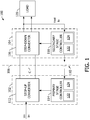
- Fig. 1 is a block diagram of an exemplary embodiment of a power converter 100.
- power converter 100 includes a primary stage 102 and a secondary stage 104.
- Primary stage 102 is coupled in electrical isolation from secondary stage 104, such as by galvanic isolation, due to an isolation barrier 106 comprising transformers, inductors, or capacitors, etc.
- isolation barrier 106 comprising transformers, inductors, or capacitors, etc.
- primary stage 102 has a primary ground structure (not shown) and secondary stage 104 has a secondary ground structure (not shown).
- Isolation barrier 106 separates the primary ground structure from the secondary ground structure.
- Isolation barrier 106 also separates an input voltage V in from an output voltage V out on either side of isolation barrier 106.
- the isolation barrier includes at least one optocoupler 110 that communicatively couples primary stage 102 and secondary stage 104 across isolation barrier 106.
- Power converter 100 may also include a DC capacitor C coupled across a DC link between primary stage 102 and secondary stage 104.
- Power converter 100 is configured to receive an input voltage V in and provide an output voltage V out .
- power converter 100 is an AC-DC converter that receives an AC input voltage and generates a DC output voltage.
- power converter 100 may be a DC-DC converter that receives a DC input voltage and converts that DC input voltage to a different DC output voltage.
- the DC input voltage may be received from a DC power source such as a rectifier (not shown) configured to convert an AC input voltage to a DC voltage.
- primary stage 102 includes a step-up converter 112 coupled to a primary stage controller 114 in primary stage 102.
- Step-up converter 112 is either a boost circuit or a power factor correction (PFC) circuit and is configured to condition input voltage V in to generate a DC boost voltage V b .
- step-up converter 112 may be any type of converter that enables power converter 100 to function as described herein.
- Primary stage controller 114 is coupled to optocoupler 110 for communicating with secondary stage 104 across isolation barrier 106.
- Primary stage controller 114 is configured to control operation of step-up converter 112 based on control signals received from secondary stage 104 across isolation barrier 106.
- Primary stage controller 114 is further configured to adjust a step-up converter reference voltage based on a load current signal indicative of a load transient, wherein the load current signal is transmitted from secondary stage 104 of isolation barrier 106.
- secondary stage 104 includes a step-down converter 116 and a secondary stage controller 118.
- Step-down converter 116 includes a buck converter or an LLC resonant converter.
- step-down converter 116 may be any type of DC-DC converter that enables power converter 100 to function as described herein.
- Step-down converter 116 is configured to condition the DC boost voltage V b received across isolation barrier 106 from step-up converter 112 to provide output voltage V out to a load 120.
- Secondary stage controller 118 is configured to control step-down converter 116 to deliver output voltage V out and output current I o to load 120.
- Secondary stage controller 118 is also configured to continuously and rapidly sample output current I o being delivered to load 120 to monitor for a load transient.
- Secondary stage controller 118 is configured to generate and transmit a signal representing measured load current I o .
- Measured load current I o may be transmitted to primary stage controller 114 continuously at predetermined intervals, when a transient is measured, or when a transient greater than a threshold is measured.
- the measured load current signal I o is transmitted by secondary stage controller 118 using pulse width modulation (PWM) or pulse frequency modulation (PFM).
- PWM pulse width modulation
- PFM pulse frequency modulation
- primary and secondary stage controllers 114 and 118 are each implemented by a processor 122 communicatively coupled to a memory device 124 for executing instructions.
- executable instructions are stored in memory device 124.
- controllers 114 and 118 may be implemented using any circuitry that enables controllers 114 and 118 to control operation of primary and secondary stages 102 and 104, respectively, as described herein.
- controllers 114 and 118 may include a state machine that learns or is pre-programmed to determine information relevant to load 120 requiring power.
- controllers 114 and 118 may dynamically determine what power resources will be needed and at what performance level and environmental conditions (e.g., temperature, humidity, time of day, etc.) those power resources will need to operate. Controllers 114 and 118 may perform dynamic monitoring to determine whether a given load 120 is satisfied with the power delivered, and whether delivered power is free of harmonics, transients, etc. In some embodiments, dynamic monitoring may include tracking resource usage to determine how much current or voltage should be delivered. Controllers 114 and 118 may also monitor and/or control rapidity (i.e., bandwidth) and inverter capability (e.g., overload, reactive power, active power) to facilitate ensuring reliability of system 100 and minimizing performance degradation.
- rapidity i.e., bandwidth
- inverter capability e.g., overload, reactive power, active power
- controllers 114 and 118 perform one or more operations described herein by programming processor 122.
- processor 122 may be programmed by encoding an operation as one or more executable instructions and by providing the executable instructions in memory device 124.
- Processor 122 may include one or more processing units (e.g., in a multi-core configuration). Further, processor 122 may be implemented using one or more heterogeneous processor systems in which a main processor is present with secondary processors on a single chip. As another illustrative example, processor 122 may be a symmetric multi-processor system containing multiple processors of the same type.
- processor 122 may be implemented using any suitable programmable circuit including one or more systems and microcontrollers, microprocessors, reduced instruction set circuits (RISC), application specific integrated circuits (ASIC), programmable logic circuits, field programmable gate arrays (FPGA), digital signal processors (DSP), and any other circuit capable of executing the functions described herein.
- processor 122 causes controllers 114 and 118 to control operation of primary and secondary stages 102 and 104, respectively, as described herein.
- memory device 124 is one or more devices that enable information such as executable instructions and/or other data to be stored and retrieved.
- Memory device 124 may include one or more computer readable media, such as, without limitation, dynamic random access memory (DRAM), static random access memory (SRAM), a solid state disk, and/or a hard disk.
- Memory device 124 may be configured to store, without limitation, application source code, application object code, source code portions of interest, object code portions of interest, configuration data, execution events and/or any other type of data.
- Fig. 2 is a graph 200 showing current and voltage characteristics of selected components of power converter 100 (shown in FIG. 1 ) during a load transient.
- secondary stage controller 118 communicates an actual value of measured load current signal I o to primary stage controller 114 using a PWM signal.
- Primary stage controller 114 receives a measured load current signal I' o . Because it is communicated across isolation barrier 106, the measured load current signal I' o steadily increases with a slight time delay d1.
- secondary stage controller 118 may communicate a differentiation signal Î' o .
- the differentiation signal Î' o goes either positive or negative when there is a change in the load current I o , rather than communicating an actual value of the load current I o .
- secondary stage controller 118 pulses a value of 1 to primary stage controller 114 when a large change in the load current occurs.
- Secondary stage controller 118 may be programmed with various thresholds defining when to indicate a load transient. For example, if a measured current change is below a predefined threshold, secondary stage controller 118 does not communicate the differentiation signal Î' o .
- secondary stage controller 118 may transmit a double pulse of the value 1, rather than pulsing a value of -1. Further, secondary stage controller 118 may pulse only the initial value of 1 indicating the start of a transient and may not pulse any representation of the value of -1.
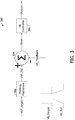
- Fig. 3 is a block diagram of an exemplary control loop 300 implemented by primary stage controller 114 (shown in Fig. 1 ).
- Primary stage controller 114 includes control loop 300 for regulating the boost voltage V b , the voltage across capacitor C.
- Primary stage controller 114 includes a target voltage V b target * as an input.
- the target voltage V b target * may be provided by primary stage controller 114, an external signal communicated to primary stage controller 114, using a peak of the AC input voltage, or from secondary stage controller 118.
- Primary stage controller 114 also includes a reference voltage V b * at an output of primary stage controller 114.
- the reference voltage V b * of the control loop follows the target voltage V b target * using a profiling mechanism 302. For example, if the target voltage V b target * changes as a step, then the reference voltage V b * will follow the target voltage V b target * as a ramp or a polynomial.
- Primary stage controller 114 then calculates an error by subtracting a feedback voltage V b_ feedback from reference voltage V b * at a summing junction 304. Using the calculated error, a boost voltage controller 306 manipulates the reference voltage V b * to output a boost voltage V b to respond to an increase in load current I o . In normal steady state operation, the target voltage V b target * will go up or down and the reference voltage V b * will follow it by ramping up or ramping down.
- primary stage controller 114 when a sudden increase in load current I o is detected, primary stage controller 114 introduces a step change in the reference voltage V b * . More specifically, upon receiving signal Î' o indicating a load transient, primary stage controller 114 introduces an artificial spike 202 in the reference voltage V b * .
- artificial spike 202 may be introduced through isolation barrier 106 as a separate signal or through communication lines. Artificial spike 202 causes additional charge to accumulate in capacitor C such that when load 120 demands a spike in current, power converter 100 is able to deliver it.
- Control loop 300 quickly responds to artificial spike 202 as is shown by a ramping 204 of boost voltage V b .
- a bandwidth BW b of primary stage controller 114 is increased.
- the bandwidth BW b tends to be lower relative to during a transient, which reduces ripple in load current I o and output voltage V o in spite of the alternating input voltage V in and current I in .
- This bandwidth BW b is increased during transients to increase the voltage in capacitor C as quickly as possible without having to worry about ripple.
- the bandwidth BW b increases, primary stage controller 114 responds very quickly, and capacitor C delivers the current to load 120.
- artificial spike 202 has a value of delta ⁇ .
- ⁇ may be determined using a variety of methods. For example, ⁇ may be based on an increase in voltage with respect to the fixed target voltage or reference voltage over a period of time. ⁇ may be based on a percentage of the reference voltage, or it could be defined by maximum and minimum values where the increase in load 120 demand is unknown. ⁇ may also be a function of an increase in output current I o or output power. ⁇ may jump to a predetermined value, which may be a function of the AC input voltage V in . ⁇ could be based on the peak of input voltage V in , or it could be related to the maximum voltage rating of the capacitor C. ⁇ is chosen based on the specific application for each particular power converter.
- a predetermined delay d2 may be provided between artificial spike 202 and the ramp down 206 of the boost voltage V b .
- Predetermined delay d2 may be a fixed delay, or it may be based on one or more of output power, output current, output voltage, input voltage, and the target voltage V b target *
- primary stage controller 114 increases the boost reference voltage V b * by introducing artificial spike 202 having a ⁇ value near a safe maximum value, which is peak AC input voltage V in .
- Artificial spike 202 causes step-up converter 112 to increase its output and quickly flood capacitor C.
- primary stage controller 114 also increases its bandwidth BW b during a transient to flood capacitor C faster. Because the target voltage V b target * is not changed, the reference voltage V b * will ramp back to the target value, making the reference change temporary. Primary stage controller 114 bandwidth BW b also ramps back to its steady state value to deliver minimal output ripple.
- primary stage controller 114 Upon a load drop, primary stage controller 114 decreases the boost reference voltage V b * by introducing artificial spike 202 having a ⁇ value near a safe minimum value, which is the negative peak AC input voltage V in . Primary stage controller 114 also increases its bandwidth BW b . Because the target voltage V b target * is not changed, the reference voltage V b * will ramp back to the target value, making the reference change temporary. Primary stage controller 114 bandwidth BW b also ramps back to its steady state value to deliver minimal output ripple.
- An exemplary technical effect of the methods and systems described herein includes at least one of: (a) electrically isolating a primary stage and a secondary stage of a power conversion system using an isolation barrier; and (b) adjusting, by a primary stage controller positioned in the primary stage, a step-up converter reference voltage based on a load current signal indicative of a load transient, the load current signal transmitted from the secondary stage.
- a primary stage controller monitors load current measurements provided over an isolation barrier by a secondary stage controller. When a change in the load current exceeds a predetermined threshold value, the primary stage controller adjusts a boost output voltage reference to flood a DC link capacitor and increase the available voltage to meet the load demand.
Landscapes
- Engineering & Computer Science (AREA)
- Power Engineering (AREA)
- Dc-Dc Converters (AREA)
Abstract
Description
- The field of the invention relates generally to power conversion systems, and more specifically, to improving load transient response in power conversion systems.
- Rectifiers that employ a boost and buck converter architecture or a power factor correction (PFC) circuit and an inductor-inductor-capacitor (LLC) converter architecture are popular because of their flexibility, range of operation, and ability reach higher overall efficiency. Each converter has its own controller, typically including multiple cascaded control loops for output voltage, input current, and an outer boost voltage loop. During a fast load transient, it is important to coordinate all these loops across voltage boundaries to minimize output voltage fluctuation.
- At least some known rectifiers include a single controller having isolated analog and digital inputs and outputs to maintain regulation across high voltage boundaries. Such rectifiers demand more expensive digital controllers and increase an overall part count and cost, which often lack the response time necessary for proper power converter operation. Other rectifiers use disturbance rejection methods that implement more complex algorithms that require more expensive controllers and/or more parts. Many of such methods also make the output control more susceptible to measurement noise.
- In one embodiment, a power converter is provided that includes an isolation barrier having a primary stage side and a secondary stage side, a step-up converter positioned on the primary stage side, and a primary stage controller coupled to the step-up converter and positioned on the primary stage side. The step-up converter is configured to condition an input voltage and generate a direct current (DC) boost voltage. The primary stage controller is configured to adjust a step-up converter reference voltage based on a load current signal indicative of a load transient. The load current signal is transmitted from a secondary stage side of the isolation barrier.
- In another embodiment, a method is provided that includes electrically isolating a primary stage and a secondary stage of a power conversion system using an isolation barrier. The method also includes adjusting, by a primary stage controller positioned in the primary stage, a step-up converter reference voltage based on a load current signal indicative of a load transient. The load current signal is transmitted from the secondary stage.
- In yet another embodiment, a power conversion system is provided that includes a primary stage and a secondary stage, an isolation barrier electrically isolating the primary stage and the secondary stage, and a primary stage controller positioned in the primary stage. The primary stage controller is configured to adjust a step-up converter reference voltage based on a load current signal indicative of a load transient. The load current signal is transmitted from the secondary stage.
-
-
Fig. 1 is a block diagram of an exemplary embodiment of a power converter. -
Fig. 2 is a graph showing current and voltage characteristics of selected components of the power converter shown inFig. 1 during a load transient. -
Fig. 3 is a block diagram of an exemplary control loop implemented by the primary stage controller shown inFig. 1 . -
Fig. 1 is a block diagram of an exemplary embodiment of apower converter 100. In the exemplary embodiment,power converter 100 includes aprimary stage 102 and asecondary stage 104.Primary stage 102 is coupled in electrical isolation fromsecondary stage 104, such as by galvanic isolation, due to anisolation barrier 106 comprising transformers, inductors, or capacitors, etc. For example,primary stage 102 has a primary ground structure (not shown) andsecondary stage 104 has a secondary ground structure (not shown).Isolation barrier 106 separates the primary ground structure from the secondary ground structure.Isolation barrier 106 also separates an input voltage Vin from an output voltage Vout on either side ofisolation barrier 106. In some embodiments, the isolation barrier includes at least oneoptocoupler 110 that communicatively couplesprimary stage 102 andsecondary stage 104 acrossisolation barrier 106.Power converter 100 may also include a DC capacitor C coupled across a DC link betweenprimary stage 102 andsecondary stage 104. -
Power converter 100 is configured to receive an input voltage Vin and provide an output voltage Vout. In one embodiment,power converter 100 is an AC-DC converter that receives an AC input voltage and generates a DC output voltage. Alternatively,power converter 100 may be a DC-DC converter that receives a DC input voltage and converts that DC input voltage to a different DC output voltage. In such an embodiment, the DC input voltage may be received from a DC power source such as a rectifier (not shown) configured to convert an AC input voltage to a DC voltage. - In the exemplary embodiment,
primary stage 102 includes a step-up converter 112 coupled to aprimary stage controller 114 inprimary stage 102. Step-up converter 112 is either a boost circuit or a power factor correction (PFC) circuit and is configured to condition input voltage Vin to generate a DC boost voltage Vb. Alternatively, step-up converter 112 may be any type of converter that enablespower converter 100 to function as described herein.Primary stage controller 114 is coupled tooptocoupler 110 for communicating withsecondary stage 104 acrossisolation barrier 106.Primary stage controller 114 is configured to control operation of step-up converter 112 based on control signals received fromsecondary stage 104 acrossisolation barrier 106.Primary stage controller 114 is further configured to adjust a step-up converter reference voltage based on a load current signal indicative of a load transient, wherein the load current signal is transmitted fromsecondary stage 104 ofisolation barrier 106. - In the exemplary embodiment,
secondary stage 104 includes a step-down converter 116 and asecondary stage controller 118. Step-down converter 116 includes a buck converter or an LLC resonant converter. Alternatively, step-down converter 116 may be any type of DC-DC converter that enablespower converter 100 to function as described herein. Step-down converter 116 is configured to condition the DC boost voltage Vb received acrossisolation barrier 106 from step-up converter 112 to provide output voltage Vout to aload 120.Secondary stage controller 118 is configured to control step-down converter 116 to deliver output voltage Vout and output current Io to load 120.Secondary stage controller 118 is also configured to continuously and rapidly sample output current Io being delivered to load 120 to monitor for a load transient. -
Secondary stage controller 118 is configured to generate and transmit a signal representing measured load current Io. Measured load current Io may be transmitted toprimary stage controller 114 continuously at predetermined intervals, when a transient is measured, or when a transient greater than a threshold is measured. In the exemplary embodiment, the measured load current signal Io is transmitted bysecondary stage controller 118 using pulse width modulation (PWM) or pulse frequency modulation (PFM). - In the exemplary embodiment, primary and
secondary stage controllers processor 122 communicatively coupled to amemory device 124 for executing instructions. In some embodiments, executable instructions are stored inmemory device 124. Alternatively,controllers controllers secondary stages controllers controllers Controllers load 120 is satisfied with the power delivered, and whether delivered power is free of harmonics, transients, etc. In some embodiments, dynamic monitoring may include tracking resource usage to determine how much current or voltage should be delivered.Controllers system 100 and minimizing performance degradation. - In the exemplary embodiment,
controllers programming processor 122. For example,processor 122 may be programmed by encoding an operation as one or more executable instructions and by providing the executable instructions inmemory device 124.Processor 122 may include one or more processing units (e.g., in a multi-core configuration). Further,processor 122 may be implemented using one or more heterogeneous processor systems in which a main processor is present with secondary processors on a single chip. As another illustrative example,processor 122 may be a symmetric multi-processor system containing multiple processors of the same type. Further,processor 122 may be implemented using any suitable programmable circuit including one or more systems and microcontrollers, microprocessors, reduced instruction set circuits (RISC), application specific integrated circuits (ASIC), programmable logic circuits, field programmable gate arrays (FPGA), digital signal processors (DSP), and any other circuit capable of executing the functions described herein. In the exemplary embodiment,processor 122 causescontrollers secondary stages - In the exemplary embodiment,
memory device 124 is one or more devices that enable information such as executable instructions and/or other data to be stored and retrieved.Memory device 124 may include one or more computer readable media, such as, without limitation, dynamic random access memory (DRAM), static random access memory (SRAM), a solid state disk, and/or a hard disk.Memory device 124 may be configured to store, without limitation, application source code, application object code, source code portions of interest, object code portions of interest, configuration data, execution events and/or any other type of data. -
Fig. 2 is agraph 200 showing current and voltage characteristics of selected components of power converter 100 (shown inFIG. 1 ) during a load transient. In the exemplary embodiment,secondary stage controller 118 communicates an actual value of measured load current signal Io toprimary stage controller 114 using a PWM signal.Primary stage controller 114 receives a measured load current signal I'o. Because it is communicated acrossisolation barrier 106, the measured load current signal I'o steadily increases with a slight time delay d1. - In an alternative embodiment, rather than the measured load current signal I'o,
secondary stage controller 118 may communicate a differentiation signal Î'o. The differentiation signal Î'o. goes either positive or negative when there is a change in the load current Io, rather than communicating an actual value of the load current Io. More specifically,secondary stage controller 118 pulses a value of 1 toprimary stage controller 114 when a large change in the load current occurs.Secondary stage controller 118 may be programmed with various thresholds defining when to indicate a load transient. For example, if a measured current change is below a predefined threshold,secondary stage controller 118 does not communicate the differentiation signal Î'o. Additionally, or alternatively,secondary stage controller 118 may transmit a double pulse of the value 1, rather than pulsing a value of -1. Further,secondary stage controller 118 may pulse only the initial value of 1 indicating the start of a transient and may not pulse any representation of the value of -1. -
Fig. 3 is a block diagram of anexemplary control loop 300 implemented by primary stage controller 114 (shown inFig. 1 ).Primary stage controller 114 includescontrol loop 300 for regulating the boost voltage Vb, the voltage across capacitor C.Primary stage controller 114 includes a target voltage

primary stage controller 114, an external signal communicated toprimary stage controller 114, using a peak of the AC input voltage, or fromsecondary stage controller 118.Primary stage controller 114 also includes a reference voltage
primary stage controller 114. The reference voltage

profiling mechanism 302. For example, if the target voltage


-
Primary stage controller 114 then calculates an error by subtracting a feedback voltage Vb_feedback from reference voltage
junction 304. Using the calculated error, aboost voltage controller 306 manipulates the reference voltage


- In the exemplary embodiment, assuming the target voltage

primary stage controller 114 introduces a step change in the reference voltage
primary stage controller 114 introduces anartificial spike 202 in the reference voltage
artificial spike 202 may be introduced throughisolation barrier 106 as a separate signal or through communication lines.Artificial spike 202 causes additional charge to accumulate in capacitor C such that whenload 120 demands a spike in current,power converter 100 is able to deliver it.Control loop 300 quickly responds toartificial spike 202 as is shown by a ramping 204 of boost voltage Vb. - In one embodiment, for
control loop 300 to more quickly respond toartificial spike 202, a bandwidth BWb ofprimary stage controller 114 is increased. During steady state operation, the bandwidth BWb tends to be lower relative to during a transient, which reduces ripple in load current Io and output voltage Vo in spite of the alternating input voltage Vin and current Iin. To maintain the output as stable as possible to minimize ripple, it is normal for the control loop to have a relatively lower steady state bandwidth BWb. This bandwidth BWb is increased during transients to increase the voltage in capacitor C as quickly as possible without having to worry about ripple. As a result, the bandwidth BWb increases,primary stage controller 114 responds very quickly, and capacitor C delivers the current to load 120. - In the exemplary embodiment,
artificial spike 202 has a value of delta Δ. Δ may be determined using a variety of methods. For example, Δ may be based on an increase in voltage with respect to the fixed target voltage or reference voltage over a period of time. Δ may be based on a percentage of the reference voltage, or it could be defined by maximum and minimum values where the increase inload 120 demand is unknown. Δ may also be a function of an increase in output current Io or output power. Δ may jump to a predetermined value, which may be a function of the AC input voltage Vin. Δ could be based on the peak of input voltage Vin, or it could be related to the maximum voltage rating of the capacitor C. Δ is chosen based on the specific application for each particular power converter. - A predetermined delay d2 may be provided between
artificial spike 202 and the ramp down 206 of the boost voltage Vb. Predetermined delay d2 may be a fixed delay, or it may be based on one or more of output power, output current, output voltage, input voltage, and the target voltage
- During operation, in the exemplary embodiment, upon a load step,
primary stage controller 114 increases the boost reference voltage
artificial spike 202 having a Δ value near a safe maximum value, which is peak AC input voltage Vin.Artificial spike 202 causes step-upconverter 112 to increase its output and quickly flood capacitor C. In some embodiments,primary stage controller 114 also increases its bandwidth BWb during a transient to flood capacitor C faster. Because the target voltage

Primary stage controller 114 bandwidth BWb also ramps back to its steady state value to deliver minimal output ripple. - Upon a load drop,
primary stage controller 114 decreases the boost reference voltage
artificial spike 202 having a Δ value near a safe minimum value, which is the negative peak AC input voltage Vin.Primary stage controller 114 also increases its bandwidth BWb. Because the target voltage

Primary stage controller 114 bandwidth BWb also ramps back to its steady state value to deliver minimal output ripple. - An exemplary technical effect of the methods and systems described herein includes at least one of: (a) electrically isolating a primary stage and a secondary stage of a power conversion system using an isolation barrier; and (b) adjusting, by a primary stage controller positioned in the primary stage, a step-up converter reference voltage based on a load current signal indicative of a load transient, the load current signal transmitted from the secondary stage.
- The embodiments described herein facilitate improving load transient response in power converters. A primary stage controller monitors load current measurements provided over an isolation barrier by a secondary stage controller. When a change in the load current exceeds a predetermined threshold value, the primary stage controller adjusts a boost output voltage reference to flood a DC link capacitor and increase the available voltage to meet the load demand.
- This written description uses examples to disclose the invention, and also to enable any person skilled in the art to practice the invention, including making and using any devices or systems and performing any incorporated methods. The patentable scope of the invention is defined by the claims, and may include other examples that occur to those skilled in the art. Such other examples are intended to be within the scope of the claims if they have structural elements that do not differ from the literal language of the claims, or if they include equivalent structural elements with insubstantial differences from the literal languages of the claims.
- Various aspects and embodiments of the present invention are defined by the following numbered clauses:
- 1. A power converter comprising:
- an isolation barrier having a primary stage side and a secondary stage side;
- a step-up converter positioned on said primary stage side, said step-up converter configured to condition an input voltage and generate a direct current (DC) boost voltage; and
- a primary stage controller positioned on said primary stage side and coupled to said step-up converter, said primary stage controller configured to adjust a step-up converter reference voltage based on a load current signal indicative of a load transient, the load current signal transmitted from a secondary stage side of said isolation barrier.
- 2. The converter of clause 1, wherein said step-up converter comprises one of a boost circuit and a power factor correction (PFC) circuit.
- 3. The converter of any preceding clause, further comprising a secondary stage controller coupled to a step-down converter on said secondary stage side, said step-down converter coupled to an output of said said step-up converter, said secondary stage controller configured to measure a load current provided to a load by said step-down converter and transmit the load current signal to said primary stage controller.
- 4. The converter of any preceding clause, further comprising an optocoupler configured to enable communication between said primary and secondary stage sides across said isolation barrier.
- 5. The converter of any preceding clause, further comprising a DC capacitor coupled across a DC link between said primary and secondary stage sides, wherein said DC capacitor is also coupled to an output of said step-up converter.
- 6. The converter of any preceding clause, wherein to adjust the step-up converter reference voltage, said primary stage controller is further configured to momentarily adjust an input current reference such that a charge rate of said DC capacitor increases to enable said power converter to provide sufficient power during the load transient.
- 7. The converter of any preceding clause, wherein said primary stage controller increases in bandwidth during the load transient to increase a response time of said primary stage controller.
- 8. A method comprising:
- electrically isolating a primary stage and a secondary stage of a power conversion system using an isolation barrier; and
- adjusting, by a primary stage controller positioned in the primary stage, a step-up converter reference voltage based on a load current signal indicative of a load transient, the load current signal transmitted from the secondary stage.
- 9. The method of any preceding clause, further comprising:
- measuring, by a secondary stage controller positioned in the secondary stage, a load current provided to a load by a step-down converter; and
- transmitting the load current signal to the primary stage controller.
- 10. The method of any preceding clause, wherein transmitting the load current signal to the primary stage controller further comprises transmitting the load current signal to the primary stage controller across the isolation barrier via an optocoupler.
- 11. The method of any preceding clause, wherein transmitting the load current signal to the primary stage controller further comprises one of continuously transmitting the load current signal and transmitting the load current signal when a change the measured load current exceeds a predetermined threshold.
- 12. The method of any preceding clause, wherein adjusting a step-up converter reference voltage further comprises momentarily adjusting an input current reference such that a charge rate of said DC capacitor increases to enable said power converter to provide sufficient power during the load transient.
- 13. A power conversion system comprising:
- a primary stage and a secondary stage;
- an isolation barrier electrically isolating the primary stage and the secondary stage; and
- a primary stage controller positioned in the primary stage, said primary stage controller configured to adjust a step-up converter reference voltage based on a load current signal indicative of a load transient, the load current signal transmitted from the secondary stage.
- 14. The system of any preceding clause, further comprising a step-up converter communicatively coupled to said primary stage controller in the primary stage, said step-up converter configured to condition an input voltage and generate a direct current (DC) boost voltage.
- 15. The system of any preceding clause, wherein said step-up converter comprises one of a boost circuit and a power factor correction (PFC) circuit.
- 16. The system of any preceding clause, further comprising:
- a step-down converter positioned in the secondary stage, said step-down converter configured to condition the DC boost voltage to generate a DC output voltage for use by a load; and
- a secondary stage controller communicatively coupled to said step-down converter, said secondary stage controller configured to measure a load current provided to the load by said step-down converter and transmit the load current signal to said primary stage controller.
- 17. The system of any preceding clause, wherein said step-down converter comprises one of a buck converter and an inductor-inductor-capacitor (LLC) converter.
- 18. The system of any preceding clause, further comprising an optocoupler configured to enable communication between said primary and secondary stages across said isolation barrier.
- 19. The system of any preceding clause, further comprising a DC capacitor coupled across a DC link between the primary stage and the secondary stage, wherein to adjust the step-up converter reference voltage, said primary stage controller is further configured to momentarily adjust an input current reference such that a charge rate of said DC capacitor increases to enable said power converter to provide sufficient power during the load transient.
- 20. The system of any preceding clause, wherein said primary stage controller increases in bandwidth during the load transient to increase a response time of said primary stage controller.
Claims (11)
- A power converter (100) comprising:an isolation barrier (106) having a primary stage (102) side and a secondary stage (104) side;a step-up converter (112) positioned on said primary stage side, said step-up converter configured to condition an input voltage and generate a direct current (DC) boost voltage; anda primary stage controller (114) positioned on said primary stage side and coupled to said step-up converter, said primary stage controller configured to adjust a step-up converter reference voltage based on a load current signal indicative of a load transient, the load current signal transmitted from a secondary stage side of said isolation barrier.
- The converter of claim 1, wherein said step-up converter (112) comprises one of a boost circuit and a power factor correction (PFC) circuit.
- The converter of claim 1 or 2, further comprising a secondary stage controller (118) coupled to a step-down converter (116) on said secondary stage (104) side, said step-down converter coupled to an output of said said step-up converter (112), said secondary stage controller configured to measure a load current provided to a load (120) by said step-down converter and transmit the load current signal to said primary stage controller (114).
- The converter of claim 3, further comprising an optocoupler (110) configured to enable communication between said primary and secondary stage (102, 104) sides across said isolation barrier (106).
- The converter of any of claims 1 to 4, further comprising a DC capacitor coupled across a DC link between said primary and secondary stage (104) sides, wherein said DC capacitor is also coupled to an output of said step-up converter (112).
- The converter of claim 5, wherein to adjust the step-up converter (112) reference voltage, said primary stage (102) controller is further configured to momentarily adjust an input current reference such that a charge rate of said DC capacitor increases to enable said power converter (100) to provide sufficient power during the load (120) transient.
- A power conversion system comprising:a primary stage (102) and a secondary stage (104);an isolation barrier (106) electrically isolating the primary stage and the secondary stage; anda primary stage controller (114) positioned in the primary stage, said primary stage controller configured to adjust a step-up converter reference voltage based on a load current signal indicative of a load transient, the load current signal transmitted from the secondary stage.
- The system of claim 7, further comprising a step-up converter (112) communicatively coupled to said primary stage controller (114) in the primary stage (102), said step-up converter configured to condition an input voltage and generate a direct current (DC) boost voltage.
- The system of claim 8, further comprising:a step-down converter (116) positioned in the secondary stage (104), said step-down converter configured to condition the DC boost voltage to generate a DC output voltage for use by a load (120); anda secondary stage controller (118) communicatively coupled to said step-down converter, said secondary stage controller configured to measure a load current provided to the load by said step-down converter and transmit the load current signal to said primary stage controller (114).
- The system of claim 7, 8 or 9, wherein said primary stage controller (114) increases in bandwidth during the load transient to increase a response time of said primary stage controller.
- A method comprising:electrically isolating a primary stage and a secondary stage of a power conversion system using an isolation barrier; andadjusting, by a primary stage controller positioned in the primary stage, a step-up converter reference voltage based on a load current signal indicative of a load transient, the load current signal transmitted from the secondary stage.
Applications Claiming Priority (1)
| Application Number | Priority Date | Filing Date | Title |
|---|---|---|---|
| US14/612,956 US9374001B1 (en) | 2015-02-03 | 2015-02-03 | Improving load transient response by adjusting reference current in isolated power converters |
Publications (2)
| Publication Number | Publication Date |
|---|---|
| EP3054573A1 true EP3054573A1 (en) | 2016-08-10 |
| EP3054573B1 EP3054573B1 (en) | 2019-09-25 |
Family
ID=55299249
Family Applications (1)
| Application Number | Title | Priority Date | Filing Date |
|---|---|---|---|
| EP16153117.3A Active EP3054573B1 (en) | 2015-02-03 | 2016-01-28 | Methods and systems for improving load transient response in power conversion systems |
Country Status (3)
| Country | Link |
|---|---|
| US (1) | US9374001B1 (en) |
| EP (1) | EP3054573B1 (en) |
| CN (1) | CN105846659B (en) |
Families Citing this family (21)
| Publication number | Priority date | Publication date | Assignee | Title |
|---|---|---|---|---|
| US10680515B2 (en) | 2011-05-05 | 2020-06-09 | Psemi Corporation | Power converters with modular stages |
| KR101556838B1 (en) | 2011-05-05 | 2015-10-13 | 아크틱 샌드 테크놀로지스, 인크. | Dc-dc converter with modular stages |
| US8743553B2 (en) | 2011-10-18 | 2014-06-03 | Arctic Sand Technologies, Inc. | Power converters with integrated capacitors |
| US9878635B1 (en) * | 2013-02-13 | 2018-01-30 | University Of Maryland | Powertrain system in plug-in electric vehicles |
| US8724353B1 (en) | 2013-03-15 | 2014-05-13 | Arctic Sand Technologies, Inc. | Efficient gate drivers for switched capacitor converters |
| US8619445B1 (en) | 2013-03-15 | 2013-12-31 | Arctic Sand Technologies, Inc. | Protection of switched capacitor power converter |
| TW201640796A (en) | 2015-03-13 | 2016-11-16 | 亞提克聖德技術股份有限公司 | DC-to-DC transformer with inductor for promoting energy transfer between capacitors |
| WO2017007991A1 (en) | 2015-07-08 | 2017-01-12 | Arctic Sand Technologies, Inc. | Switched-capacitor power converters |
| US11258371B2 (en) * | 2016-02-16 | 2022-02-22 | Psemi Corporation | Switched capacitors for AC-DC applications |
| US10250058B2 (en) * | 2016-09-15 | 2019-04-02 | Raytheon Company | Charge management system |
| CN108512421B (en) * | 2018-04-24 | 2019-08-27 | 上海推拓科技有限公司 | A PFWM Control Method |
| CN111835214B (en) * | 2019-04-23 | 2021-08-06 | 通嘉科技股份有限公司 | Method for sending and receiving commands between a master controller and a slave controller for a power converter |
| CN110941322A (en) * | 2019-12-06 | 2020-03-31 | 苏州浪潮智能科技有限公司 | A method and system for optimizing server power |
| CN111510005B (en) * | 2020-05-28 | 2021-11-09 | 苏州浪潮智能科技有限公司 | PSU applied to high-density GPU and power supply system |
| TWI748888B (en) * | 2021-03-03 | 2021-12-01 | 威綸科技股份有限公司 | Starting adjustment circuit and flyback power starting system |
| CN113156219B (en) * | 2021-05-10 | 2024-03-29 | 郑州大学 | Method and device for monitoring output capacitance value and degradation status of Boost PFC converter |
| CN116232056A (en) * | 2021-12-06 | 2023-06-06 | 台达电子企业管理(上海)有限公司 | Power conversion device and voltage control method |
| CN115208178B (en) * | 2022-07-01 | 2024-05-17 | 超聚变数字技术有限公司 | Cascade converter and control method thereof |
| CN115313863B (en) * | 2022-08-08 | 2023-05-26 | 深圳创客恒源科技有限公司 | Circuit and method for regulating PFC and LLC topology output voltage based on output demand |
| CN119448737A (en) * | 2023-08-07 | 2025-02-14 | 成都芯源系统有限公司 | A power supply control circuit and control method thereof |
| CN119543628A (en) * | 2023-08-28 | 2025-02-28 | 株式会社村田制作所 | Method and device for controlling PFC |
Citations (2)
| Publication number | Priority date | Publication date | Assignee | Title |
|---|---|---|---|---|
| US20140091720A1 (en) * | 2012-09-28 | 2014-04-03 | Power Systems Technologies, Ltd. | Controller for Use with a Power Converter and Method of Operating the Same |
| US20140167648A1 (en) * | 2012-12-18 | 2014-06-19 | Richtek Technology Corporation | Power converter circuit for low power illumination device, control circuit thereof and method thereof |
Family Cites Families (17)
| Publication number | Priority date | Publication date | Assignee | Title |
|---|---|---|---|---|
| US5929692A (en) | 1997-07-11 | 1999-07-27 | Computer Products Inc. | Ripple cancellation circuit with fast load response for switch mode voltage regulators with synchronous rectification |
| US5994882A (en) | 1998-11-03 | 1999-11-30 | Linear Technology Corporation | Synchronous rectifier for boost converters |
| AUPS118302A0 (en) | 2002-03-18 | 2002-04-18 | Rectifier Technologies Pacific Pty Ltd | Wide bandwidth ac-dc converter |
| US8237530B2 (en) | 2009-08-10 | 2012-08-07 | Volterra Semiconductor Corporation | Coupled inductor with improved leakage inductance control |
| JP3717492B2 (en) * | 2003-04-16 | 2005-11-16 | ローム株式会社 | Power supply |
| US7479769B2 (en) * | 2003-08-29 | 2009-01-20 | Nxp B.V. | Power delivery system having cascaded buck stages |
| US6897641B1 (en) | 2004-06-24 | 2005-05-24 | Edward Herbert | Buck (or boost) converter with very fast output current transitions and low ripple voltage |
| US20070170897A1 (en) | 2006-01-26 | 2007-07-26 | Advanced Analogic Technologies, Inc. | High-Frequency Power MESFET Buck Switching Power Supply |
| TW200810359A (en) * | 2006-08-04 | 2008-02-16 | Richtek Technology Corp | Control circuit and method for a constant on-time PWM switching converter |
| US7639520B1 (en) * | 2007-02-26 | 2009-12-29 | Network Appliance, Inc. | Efficient power supply |
| US8004260B2 (en) * | 2009-03-26 | 2011-08-23 | Delta Electronics, Inc. | Method and apparatus for multi-stage power supplies |
| WO2011001369A2 (en) * | 2009-07-03 | 2011-01-06 | Koninklijke Philips Electronics N.V. | Low cost power supply circuit and method |
| TWI411901B (en) * | 2010-08-23 | 2013-10-11 | Anpec Electronics Corp | Switching regulator |
| US9071141B2 (en) | 2011-04-08 | 2015-06-30 | Virginia Tech Intellectual Properties, Inc. | Two-stage single phase bi-directional PWM power converter with DC link capacitor reduction |
| US9190898B2 (en) * | 2012-07-06 | 2015-11-17 | Power Systems Technologies, Ltd | Controller for a power converter and method of operating the same |
| CN103414342A (en) | 2013-07-02 | 2013-11-27 | 西南交通大学 | Fixed-frequency constant on-off time control method of dynamic voltage regulating switch converter |
| US20150028823A1 (en) * | 2013-07-24 | 2015-01-29 | Analog Devices Technology | Pulse width modulated power regulator with loop stabilizer |
-
2015
- 2015-02-03 US US14/612,956 patent/US9374001B1/en active Active
-
2016
- 2016-01-28 EP EP16153117.3A patent/EP3054573B1/en active Active
- 2016-02-03 CN CN201610075335.9A patent/CN105846659B/en active Active
Patent Citations (2)
| Publication number | Priority date | Publication date | Assignee | Title |
|---|---|---|---|---|
| US20140091720A1 (en) * | 2012-09-28 | 2014-04-03 | Power Systems Technologies, Ltd. | Controller for Use with a Power Converter and Method of Operating the Same |
| US20140167648A1 (en) * | 2012-12-18 | 2014-06-19 | Richtek Technology Corporation | Power converter circuit for low power illumination device, control circuit thereof and method thereof |
Also Published As
| Publication number | Publication date |
|---|---|
| EP3054573B1 (en) | 2019-09-25 |
| CN105846659A (en) | 2016-08-10 |
| US9374001B1 (en) | 2016-06-21 |
| CN105846659B (en) | 2020-08-18 |
Similar Documents
| Publication | Publication Date | Title |
|---|---|---|
| EP3054573B1 (en) | Methods and systems for improving load transient response in power conversion systems | |
| US8154264B2 (en) | Method and systems for conduction mode control | |
| EP4164080A1 (en) | On-grid/off-grid scheduling method and apparatus, and energy-storage power supply system | |
| US20210013803A1 (en) | Power conversion apparatus | |
| EP3624323B1 (en) | Controller for buck dc/dc converter with effective decoupling | |
| US9520808B2 (en) | Method and system for power conversion | |
| US9882423B2 (en) | Uninterruptible power supply control | |
| US20160308438A1 (en) | Discrete narrow-band switching frequency avoidance of a switch mode power converter | |
| US20150249396A1 (en) | Dc/dc converter and control method thereof | |
| US11843273B2 (en) | Battery module and power supply system | |
| US11329488B2 (en) | Power conversion system, method for controlling converter circuit, and program | |
| TWI741625B (en) | Power conversion system for autonomous current sharing of power stages | |
| US10110011B2 (en) | Methods and apparatus for controlling power converters in parallel connection | |
| EP3247018A1 (en) | Control device for inverter | |
| KR102716638B1 (en) | Circuit and method for bus voltage fluctuation of power converter | |
| JP6994673B2 (en) | Power conversion system | |
| US9871456B2 (en) | Voltage conversion device and method of operation | |
| US12445062B2 (en) | Bipolar power supply system and control method | |
| US12113362B2 (en) | Fault-responsive power system and method using active line current balancing | |
| EP3711134B1 (en) | Voltage droop-based method in a power transmission system | |
| JP7203325B2 (en) | power system | |
| US9960636B2 (en) | Power supply system and direct-current converter thereof | |
| EP3100331B1 (en) | Voltage regulation in multi-terminal hvdc network | |
| CN121216860B (en) | Exit compensation method, PI control method and energy storage system | |
| CN121193061B (en) | Current inner loop reference current value compensation method, control method, system and medium |
Legal Events
| Date | Code | Title | Description |
|---|---|---|---|
| PUAI | Public reference made under article 153(3) epc to a published international application that has entered the european phase |
Free format text: ORIGINAL CODE: 0009012 |
|
| AK | Designated contracting states |
Kind code of ref document: A1 Designated state(s): AL AT BE BG CH CY CZ DE DK EE ES FI FR GB GR HR HU IE IS IT LI LT LU LV MC MK MT NL NO PL PT RO RS SE SI SK SM TR |
|
| AX | Request for extension of the european patent |
Extension state: BA ME |
|
| STAA | Information on the status of an ep patent application or granted ep patent |
Free format text: STATUS: REQUEST FOR EXAMINATION WAS MADE |
|
| 17P | Request for examination filed |
Effective date: 20170210 |
|
| RBV | Designated contracting states (corrected) |
Designated state(s): AL AT BE BG CH CY CZ DE DK EE ES FI FR GB GR HR HU IE IS IT LI LT LU LV MC MK MT NL NO PL PT RO RS SE SI SK SM TR |
|
| STAA | Information on the status of an ep patent application or granted ep patent |
Free format text: STATUS: EXAMINATION IS IN PROGRESS |
|
| 17Q | First examination report despatched |
Effective date: 20180220 |
|
| GRAP | Despatch of communication of intention to grant a patent |
Free format text: ORIGINAL CODE: EPIDOSNIGR1 |
|
| STAA | Information on the status of an ep patent application or granted ep patent |
Free format text: STATUS: GRANT OF PATENT IS INTENDED |
|
| INTG | Intention to grant announced |
Effective date: 20190415 |
|
| GRAS | Grant fee paid |
Free format text: ORIGINAL CODE: EPIDOSNIGR3 |
|
| GRAA | (expected) grant |
Free format text: ORIGINAL CODE: 0009210 |
|
| STAA | Information on the status of an ep patent application or granted ep patent |
Free format text: STATUS: THE PATENT HAS BEEN GRANTED |
|
| RAP1 | Party data changed (applicant data changed or rights of an application transferred) |
Owner name: ABB SCHWEIZ AG |
|
| AK | Designated contracting states |
Kind code of ref document: B1 Designated state(s): AL AT BE BG CH CY CZ DE DK EE ES FI FR GB GR HR HU IE IS IT LI LT LU LV MC MK MT NL NO PL PT RO RS SE SI SK SM TR |
|
| REG | Reference to a national code |
Ref country code: GB Ref legal event code: FG4D |
|
| REG | Reference to a national code |
Ref country code: CH Ref legal event code: EP |
|
| REG | Reference to a national code |
Ref country code: AT Ref legal event code: REF Ref document number: 1184790 Country of ref document: AT Kind code of ref document: T Effective date: 20191015 |
|
| REG | Reference to a national code |
Ref country code: IE Ref legal event code: FG4D |
|
| REG | Reference to a national code |
Ref country code: DE Ref legal event code: R096 Ref document number: 602016021094 Country of ref document: DE |
|
| REG | Reference to a national code |
Ref country code: NL Ref legal event code: MP Effective date: 20190925 |
|
| PG25 | Lapsed in a contracting state [announced via postgrant information from national office to epo] |
Ref country code: FI Free format text: LAPSE BECAUSE OF FAILURE TO SUBMIT A TRANSLATION OF THE DESCRIPTION OR TO PAY THE FEE WITHIN THE PRESCRIBED TIME-LIMIT Effective date: 20190925 Ref country code: HR Free format text: LAPSE BECAUSE OF FAILURE TO SUBMIT A TRANSLATION OF THE DESCRIPTION OR TO PAY THE FEE WITHIN THE PRESCRIBED TIME-LIMIT Effective date: 20190925 Ref country code: BG Free format text: LAPSE BECAUSE OF FAILURE TO SUBMIT A TRANSLATION OF THE DESCRIPTION OR TO PAY THE FEE WITHIN THE PRESCRIBED TIME-LIMIT Effective date: 20191225 Ref country code: LT Free format text: LAPSE BECAUSE OF FAILURE TO SUBMIT A TRANSLATION OF THE DESCRIPTION OR TO PAY THE FEE WITHIN THE PRESCRIBED TIME-LIMIT Effective date: 20190925 Ref country code: NO Free format text: LAPSE BECAUSE OF FAILURE TO SUBMIT A TRANSLATION OF THE DESCRIPTION OR TO PAY THE FEE WITHIN THE PRESCRIBED TIME-LIMIT Effective date: 20191225 Ref country code: SE Free format text: LAPSE BECAUSE OF FAILURE TO SUBMIT A TRANSLATION OF THE DESCRIPTION OR TO PAY THE FEE WITHIN THE PRESCRIBED TIME-LIMIT Effective date: 20190925 |
|
| REG | Reference to a national code |
Ref country code: LT Ref legal event code: MG4D |
|
| PG25 | Lapsed in a contracting state [announced via postgrant information from national office to epo] |
Ref country code: RS Free format text: LAPSE BECAUSE OF FAILURE TO SUBMIT A TRANSLATION OF THE DESCRIPTION OR TO PAY THE FEE WITHIN THE PRESCRIBED TIME-LIMIT Effective date: 20190925 Ref country code: GR Free format text: LAPSE BECAUSE OF FAILURE TO SUBMIT A TRANSLATION OF THE DESCRIPTION OR TO PAY THE FEE WITHIN THE PRESCRIBED TIME-LIMIT Effective date: 20191226 Ref country code: LV Free format text: LAPSE BECAUSE OF FAILURE TO SUBMIT A TRANSLATION OF THE DESCRIPTION OR TO PAY THE FEE WITHIN THE PRESCRIBED TIME-LIMIT Effective date: 20190925 |
|
| REG | Reference to a national code |
Ref country code: AT Ref legal event code: MK05 Ref document number: 1184790 Country of ref document: AT Kind code of ref document: T Effective date: 20190925 |
|
| PG25 | Lapsed in a contracting state [announced via postgrant information from national office to epo] |
Ref country code: PL Free format text: LAPSE BECAUSE OF FAILURE TO SUBMIT A TRANSLATION OF THE DESCRIPTION OR TO PAY THE FEE WITHIN THE PRESCRIBED TIME-LIMIT Effective date: 20190925 Ref country code: EE Free format text: LAPSE BECAUSE OF FAILURE TO SUBMIT A TRANSLATION OF THE DESCRIPTION OR TO PAY THE FEE WITHIN THE PRESCRIBED TIME-LIMIT Effective date: 20190925 Ref country code: NL Free format text: LAPSE BECAUSE OF FAILURE TO SUBMIT A TRANSLATION OF THE DESCRIPTION OR TO PAY THE FEE WITHIN THE PRESCRIBED TIME-LIMIT Effective date: 20190925 Ref country code: AT Free format text: LAPSE BECAUSE OF FAILURE TO SUBMIT A TRANSLATION OF THE DESCRIPTION OR TO PAY THE FEE WITHIN THE PRESCRIBED TIME-LIMIT Effective date: 20190925 Ref country code: IT Free format text: LAPSE BECAUSE OF FAILURE TO SUBMIT A TRANSLATION OF THE DESCRIPTION OR TO PAY THE FEE WITHIN THE PRESCRIBED TIME-LIMIT Effective date: 20190925 Ref country code: PT Free format text: LAPSE BECAUSE OF FAILURE TO SUBMIT A TRANSLATION OF THE DESCRIPTION OR TO PAY THE FEE WITHIN THE PRESCRIBED TIME-LIMIT Effective date: 20200127 Ref country code: AL Free format text: LAPSE BECAUSE OF FAILURE TO SUBMIT A TRANSLATION OF THE DESCRIPTION OR TO PAY THE FEE WITHIN THE PRESCRIBED TIME-LIMIT Effective date: 20190925 Ref country code: RO Free format text: LAPSE BECAUSE OF FAILURE TO SUBMIT A TRANSLATION OF THE DESCRIPTION OR TO PAY THE FEE WITHIN THE PRESCRIBED TIME-LIMIT Effective date: 20190925 Ref country code: ES Free format text: LAPSE BECAUSE OF FAILURE TO SUBMIT A TRANSLATION OF THE DESCRIPTION OR TO PAY THE FEE WITHIN THE PRESCRIBED TIME-LIMIT Effective date: 20190925 |
|
| PG25 | Lapsed in a contracting state [announced via postgrant information from national office to epo] |
Ref country code: IS Free format text: LAPSE BECAUSE OF FAILURE TO SUBMIT A TRANSLATION OF THE DESCRIPTION OR TO PAY THE FEE WITHIN THE PRESCRIBED TIME-LIMIT Effective date: 20200224 Ref country code: SK Free format text: LAPSE BECAUSE OF FAILURE TO SUBMIT A TRANSLATION OF THE DESCRIPTION OR TO PAY THE FEE WITHIN THE PRESCRIBED TIME-LIMIT Effective date: 20190925 Ref country code: CZ Free format text: LAPSE BECAUSE OF FAILURE TO SUBMIT A TRANSLATION OF THE DESCRIPTION OR TO PAY THE FEE WITHIN THE PRESCRIBED TIME-LIMIT Effective date: 20190925 Ref country code: SM Free format text: LAPSE BECAUSE OF FAILURE TO SUBMIT A TRANSLATION OF THE DESCRIPTION OR TO PAY THE FEE WITHIN THE PRESCRIBED TIME-LIMIT Effective date: 20190925 |
|
| REG | Reference to a national code |
Ref country code: DE Ref legal event code: R097 Ref document number: 602016021094 Country of ref document: DE |
|
| PG2D | Information on lapse in contracting state deleted |
Ref country code: IS |
|
| PG25 | Lapsed in a contracting state [announced via postgrant information from national office to epo] |
Ref country code: DK Free format text: LAPSE BECAUSE OF FAILURE TO SUBMIT A TRANSLATION OF THE DESCRIPTION OR TO PAY THE FEE WITHIN THE PRESCRIBED TIME-LIMIT Effective date: 20190925 Ref country code: IS Free format text: LAPSE BECAUSE OF FAILURE TO SUBMIT A TRANSLATION OF THE DESCRIPTION OR TO PAY THE FEE WITHIN THE PRESCRIBED TIME-LIMIT Effective date: 20200126 |
|
| PLBE | No opposition filed within time limit |
Free format text: ORIGINAL CODE: 0009261 |
|
| STAA | Information on the status of an ep patent application or granted ep patent |
Free format text: STATUS: NO OPPOSITION FILED WITHIN TIME LIMIT |
|
| PG25 | Lapsed in a contracting state [announced via postgrant information from national office to epo] |
Ref country code: MC Free format text: LAPSE BECAUSE OF FAILURE TO SUBMIT A TRANSLATION OF THE DESCRIPTION OR TO PAY THE FEE WITHIN THE PRESCRIBED TIME-LIMIT Effective date: 20190925 |
|
| REG | Reference to a national code |
Ref country code: CH Ref legal event code: PL |
|
| 26N | No opposition filed |
Effective date: 20200626 |
|
| GBPC | Gb: european patent ceased through non-payment of renewal fee |
Effective date: 20200128 |
|
| REG | Reference to a national code |
Ref country code: BE Ref legal event code: MM Effective date: 20200131 |
|
| PG25 | Lapsed in a contracting state [announced via postgrant information from national office to epo] |
Ref country code: GB Free format text: LAPSE BECAUSE OF NON-PAYMENT OF DUE FEES Effective date: 20200128 Ref country code: FR Free format text: LAPSE BECAUSE OF NON-PAYMENT OF DUE FEES Effective date: 20200131 Ref country code: LU Free format text: LAPSE BECAUSE OF NON-PAYMENT OF DUE FEES Effective date: 20200128 |
|
| PG25 | Lapsed in a contracting state [announced via postgrant information from national office to epo] |
Ref country code: BE Free format text: LAPSE BECAUSE OF NON-PAYMENT OF DUE FEES Effective date: 20200131 Ref country code: SI Free format text: LAPSE BECAUSE OF FAILURE TO SUBMIT A TRANSLATION OF THE DESCRIPTION OR TO PAY THE FEE WITHIN THE PRESCRIBED TIME-LIMIT Effective date: 20190925 Ref country code: LI Free format text: LAPSE BECAUSE OF NON-PAYMENT OF DUE FEES Effective date: 20200131 Ref country code: CH Free format text: LAPSE BECAUSE OF NON-PAYMENT OF DUE FEES Effective date: 20200131 |
|
| PG25 | Lapsed in a contracting state [announced via postgrant information from national office to epo] |
Ref country code: IE Free format text: LAPSE BECAUSE OF NON-PAYMENT OF DUE FEES Effective date: 20200128 |
|
| PG25 | Lapsed in a contracting state [announced via postgrant information from national office to epo] |
Ref country code: TR Free format text: LAPSE BECAUSE OF FAILURE TO SUBMIT A TRANSLATION OF THE DESCRIPTION OR TO PAY THE FEE WITHIN THE PRESCRIBED TIME-LIMIT Effective date: 20190925 Ref country code: MT Free format text: LAPSE BECAUSE OF FAILURE TO SUBMIT A TRANSLATION OF THE DESCRIPTION OR TO PAY THE FEE WITHIN THE PRESCRIBED TIME-LIMIT Effective date: 20190925 Ref country code: CY Free format text: LAPSE BECAUSE OF FAILURE TO SUBMIT A TRANSLATION OF THE DESCRIPTION OR TO PAY THE FEE WITHIN THE PRESCRIBED TIME-LIMIT Effective date: 20190925 |
|
| PG25 | Lapsed in a contracting state [announced via postgrant information from national office to epo] |
Ref country code: MK Free format text: LAPSE BECAUSE OF FAILURE TO SUBMIT A TRANSLATION OF THE DESCRIPTION OR TO PAY THE FEE WITHIN THE PRESCRIBED TIME-LIMIT Effective date: 20190925 |
|
| REG | Reference to a national code |
Ref country code: DE Ref legal event code: R081 Ref document number: 602016021094 Country of ref document: DE Owner name: ACLEAP POWER INC., TW Free format text: FORMER OWNER: ABB SCHWEIZ AG, BADEN, CH |
|
| PGFP | Annual fee paid to national office [announced via postgrant information from national office to epo] |
Ref country code: DE Payment date: 20260128 Year of fee payment: 11 |