EP3054496A1 - Material for organic electroluminescent element and organic electroluminescent element using the same - Google Patents
Material for organic electroluminescent element and organic electroluminescent element using the same Download PDFInfo
- Publication number
- EP3054496A1 EP3054496A1 EP14848256.5A EP14848256A EP3054496A1 EP 3054496 A1 EP3054496 A1 EP 3054496A1 EP 14848256 A EP14848256 A EP 14848256A EP 3054496 A1 EP3054496 A1 EP 3054496A1
- Authority
- EP
- European Patent Office
- Prior art keywords
- group
- aromatic
- organic
- light
- derivative
- Prior art date
- Legal status (The legal status is an assumption and is not a legal conclusion. Google has not performed a legal analysis and makes no representation as to the accuracy of the status listed.)
- Granted
Links
- YTXNFVJDDKXXBK-UHFFFAOYSA-N CCC1=CC2c3cc(I)ccc3OC2(C)C=C1 Chemical compound CCC1=CC2c3cc(I)ccc3OC2(C)C=C1 YTXNFVJDDKXXBK-UHFFFAOYSA-N 0.000 description 1
- MNKSJEJNCQWHFE-UHFFFAOYSA-N Ic(cc1)cc2c1[o]c1ccccc21 Chemical compound Ic(cc1)cc2c1[o]c1ccccc21 MNKSJEJNCQWHFE-UHFFFAOYSA-N 0.000 description 1
- PVZYIDRHTZBWEF-UHFFFAOYSA-N Ic1ccc2[o]c(ccc(-[n]3c(cccc4)c4c4c3cccc4)c3)c3c2c1 Chemical compound Ic1ccc2[o]c(ccc(-[n]3c(cccc4)c4c4c3cccc4)c3)c3c2c1 PVZYIDRHTZBWEF-UHFFFAOYSA-N 0.000 description 1
- UJOBWOGCFQCDNV-UHFFFAOYSA-N c(cc1)cc2c1[nH]c1c2cccc1 Chemical compound c(cc1)cc2c1[nH]c1c2cccc1 UJOBWOGCFQCDNV-UHFFFAOYSA-N 0.000 description 1
Images

Classifications
-
- C—CHEMISTRY; METALLURGY
- C09—DYES; PAINTS; POLISHES; NATURAL RESINS; ADHESIVES; COMPOSITIONS NOT OTHERWISE PROVIDED FOR; APPLICATIONS OF MATERIALS NOT OTHERWISE PROVIDED FOR
- C09K—MATERIALS FOR MISCELLANEOUS APPLICATIONS, NOT PROVIDED FOR ELSEWHERE
- C09K11/00—Luminescent materials, e.g. electroluminescent or chemiluminescent
- C09K11/06—Luminescent materials, e.g. electroluminescent or chemiluminescent containing organic luminescent materials
-
- C—CHEMISTRY; METALLURGY
- C07—ORGANIC CHEMISTRY
- C07F—ACYCLIC, CARBOCYCLIC OR HETEROCYCLIC COMPOUNDS CONTAINING ELEMENTS OTHER THAN CARBON, HYDROGEN, HALOGEN, OXYGEN, NITROGEN, SULFUR, SELENIUM OR TELLURIUM
- C07F5/00—Compounds containing elements of Groups 3 or 13 of the Periodic Table
- C07F5/02—Boron compounds
- C07F5/05—Cyclic compounds having at least one ring containing boron but no carbon in the ring
-
- C—CHEMISTRY; METALLURGY
- C09—DYES; PAINTS; POLISHES; NATURAL RESINS; ADHESIVES; COMPOSITIONS NOT OTHERWISE PROVIDED FOR; APPLICATIONS OF MATERIALS NOT OTHERWISE PROVIDED FOR
- C09K—MATERIALS FOR MISCELLANEOUS APPLICATIONS, NOT PROVIDED FOR ELSEWHERE
- C09K11/00—Luminescent materials, e.g. electroluminescent or chemiluminescent
- C09K11/02—Use of particular materials as binders, particle coatings or suspension media therefor
- C09K11/025—Use of particular materials as binders, particle coatings or suspension media therefor non-luminescent particle coatings or suspension media
-
- H—ELECTRICITY
- H05—ELECTRIC TECHNIQUES NOT OTHERWISE PROVIDED FOR
- H05B—ELECTRIC HEATING; ELECTRIC LIGHT SOURCES NOT OTHERWISE PROVIDED FOR; CIRCUIT ARRANGEMENTS FOR ELECTRIC LIGHT SOURCES, IN GENERAL
- H05B33/00—Electroluminescent light sources
- H05B33/12—Light sources with substantially two-dimensional [2D] radiating surfaces
- H05B33/20—Light sources with substantially two-dimensional [2D] radiating surfaces characterised by the chemical or physical composition or the arrangement of the material in which the electroluminescent material is embedded
-
- H—ELECTRICITY
- H10—SEMICONDUCTOR DEVICES; ELECTRIC SOLID-STATE DEVICES NOT OTHERWISE PROVIDED FOR
- H10K—ORGANIC ELECTRIC SOLID-STATE DEVICES
- H10K50/00—Organic light-emitting devices
- H10K50/10—OLEDs or polymer light-emitting diodes [PLED]
- H10K50/11—OLEDs or polymer light-emitting diodes [PLED] characterised by the electroluminescent [EL] layers
-
- H—ELECTRICITY
- H10—SEMICONDUCTOR DEVICES; ELECTRIC SOLID-STATE DEVICES NOT OTHERWISE PROVIDED FOR
- H10K—ORGANIC ELECTRIC SOLID-STATE DEVICES
- H10K85/00—Organic materials used in the body or electrodes of devices covered by this subclass
- H10K85/30—Coordination compounds
- H10K85/321—Metal complexes comprising a group IIIA element, e.g. Tris (8-hydroxyquinoline) gallium [Gaq3]
- H10K85/322—Metal complexes comprising a group IIIA element, e.g. Tris (8-hydroxyquinoline) gallium [Gaq3] comprising boron
-
- H—ELECTRICITY
- H10—SEMICONDUCTOR DEVICES; ELECTRIC SOLID-STATE DEVICES NOT OTHERWISE PROVIDED FOR
- H10K—ORGANIC ELECTRIC SOLID-STATE DEVICES
- H10K85/00—Organic materials used in the body or electrodes of devices covered by this subclass
- H10K85/30—Coordination compounds
- H10K85/341—Transition metal complexes, e.g. Ru(II)polypyridine complexes
- H10K85/342—Transition metal complexes, e.g. Ru(II)polypyridine complexes comprising iridium
-
- H—ELECTRICITY
- H10—SEMICONDUCTOR DEVICES; ELECTRIC SOLID-STATE DEVICES NOT OTHERWISE PROVIDED FOR
- H10K—ORGANIC ELECTRIC SOLID-STATE DEVICES
- H10K85/00—Organic materials used in the body or electrodes of devices covered by this subclass
- H10K85/60—Organic compounds having low molecular weight
- H10K85/615—Polycyclic condensed aromatic hydrocarbons, e.g. anthracene
- H10K85/626—Polycyclic condensed aromatic hydrocarbons, e.g. anthracene containing more than one polycyclic condensed aromatic rings, e.g. bis-anthracene
-
- H—ELECTRICITY
- H10—SEMICONDUCTOR DEVICES; ELECTRIC SOLID-STATE DEVICES NOT OTHERWISE PROVIDED FOR
- H10K—ORGANIC ELECTRIC SOLID-STATE DEVICES
- H10K85/00—Organic materials used in the body or electrodes of devices covered by this subclass
- H10K85/60—Organic compounds having low molecular weight
- H10K85/649—Aromatic compounds comprising a hetero atom
- H10K85/657—Polycyclic condensed heteroaromatic hydrocarbons
- H10K85/6572—Polycyclic condensed heteroaromatic hydrocarbons comprising only nitrogen in the heteroaromatic polycondensed ring system, e.g. phenanthroline or carbazole
-
- H—ELECTRICITY
- H10—SEMICONDUCTOR DEVICES; ELECTRIC SOLID-STATE DEVICES NOT OTHERWISE PROVIDED FOR
- H10K—ORGANIC ELECTRIC SOLID-STATE DEVICES
- H10K85/00—Organic materials used in the body or electrodes of devices covered by this subclass
- H10K85/60—Organic compounds having low molecular weight
- H10K85/649—Aromatic compounds comprising a hetero atom
- H10K85/657—Polycyclic condensed heteroaromatic hydrocarbons
- H10K85/6574—Polycyclic condensed heteroaromatic hydrocarbons comprising only oxygen in the heteroaromatic polycondensed ring system, e.g. cumarine dyes
-
- B—PERFORMING OPERATIONS; TRANSPORTING
- B32—LAYERED PRODUCTS
- B32B—LAYERED PRODUCTS, i.e. PRODUCTS BUILT-UP OF STRATA OF FLAT OR NON-FLAT, e.g. CELLULAR OR HONEYCOMB, FORM
- B32B2457/00—Electrical equipment
- B32B2457/20—Displays, e.g. liquid crystal displays, plasma displays
- B32B2457/206—Organic displays, e.g. OLED
-
- C—CHEMISTRY; METALLURGY
- C07—ORGANIC CHEMISTRY
- C07D—HETEROCYCLIC COMPOUNDS
- C07D209/00—Heterocyclic compounds containing five-membered rings, condensed with other rings, with one nitrogen atom as the only ring hetero atom
- C07D209/56—Ring systems containing three or more rings
- C07D209/80—[b, c]- or [b, d]-condensed
- C07D209/82—Carbazoles; Hydrogenated carbazoles
- C07D209/86—Carbazoles; Hydrogenated carbazoles with only hydrogen atoms, hydrocarbon or substituted hydrocarbon radicals, directly attached to carbon atoms of the ring system
-
- C—CHEMISTRY; METALLURGY
- C07—ORGANIC CHEMISTRY
- C07D—HETEROCYCLIC COMPOUNDS
- C07D307/00—Heterocyclic compounds containing five-membered rings having one oxygen atom as the only ring hetero atom
- C07D307/77—Heterocyclic compounds containing five-membered rings having one oxygen atom as the only ring hetero atom ortho- or peri-condensed with carbocyclic rings or ring systems
- C07D307/91—Dibenzofurans; Hydrogenated dibenzofurans
-
- C—CHEMISTRY; METALLURGY
- C07—ORGANIC CHEMISTRY
- C07D—HETEROCYCLIC COMPOUNDS
- C07D405/00—Heterocyclic compounds containing both one or more hetero rings having oxygen atoms as the only ring hetero atoms, and one or more rings having nitrogen as the only ring hetero atom
- C07D405/02—Heterocyclic compounds containing both one or more hetero rings having oxygen atoms as the only ring hetero atoms, and one or more rings having nitrogen as the only ring hetero atom containing two hetero rings
- C07D405/10—Heterocyclic compounds containing both one or more hetero rings having oxygen atoms as the only ring hetero atoms, and one or more rings having nitrogen as the only ring hetero atom containing two hetero rings linked by a carbon chain containing aromatic rings
-
- C—CHEMISTRY; METALLURGY
- C07—ORGANIC CHEMISTRY
- C07D—HETEROCYCLIC COMPOUNDS
- C07D405/00—Heterocyclic compounds containing both one or more hetero rings having oxygen atoms as the only ring hetero atoms, and one or more rings having nitrogen as the only ring hetero atom
- C07D405/14—Heterocyclic compounds containing both one or more hetero rings having oxygen atoms as the only ring hetero atoms, and one or more rings having nitrogen as the only ring hetero atom containing three or more hetero rings
-
- C—CHEMISTRY; METALLURGY
- C09—DYES; PAINTS; POLISHES; NATURAL RESINS; ADHESIVES; COMPOSITIONS NOT OTHERWISE PROVIDED FOR; APPLICATIONS OF MATERIALS NOT OTHERWISE PROVIDED FOR
- C09K—MATERIALS FOR MISCELLANEOUS APPLICATIONS, NOT PROVIDED FOR ELSEWHERE
- C09K2211/00—Chemical nature of organic luminescent or tenebrescent compounds
- C09K2211/10—Non-macromolecular compounds
- C09K2211/1003—Carbocyclic compounds
- C09K2211/1007—Non-condensed systems
-
- C—CHEMISTRY; METALLURGY
- C09—DYES; PAINTS; POLISHES; NATURAL RESINS; ADHESIVES; COMPOSITIONS NOT OTHERWISE PROVIDED FOR; APPLICATIONS OF MATERIALS NOT OTHERWISE PROVIDED FOR
- C09K—MATERIALS FOR MISCELLANEOUS APPLICATIONS, NOT PROVIDED FOR ELSEWHERE
- C09K2211/00—Chemical nature of organic luminescent or tenebrescent compounds
- C09K2211/10—Non-macromolecular compounds
- C09K2211/1003—Carbocyclic compounds
- C09K2211/1011—Condensed systems
-
- C—CHEMISTRY; METALLURGY
- C09—DYES; PAINTS; POLISHES; NATURAL RESINS; ADHESIVES; COMPOSITIONS NOT OTHERWISE PROVIDED FOR; APPLICATIONS OF MATERIALS NOT OTHERWISE PROVIDED FOR
- C09K—MATERIALS FOR MISCELLANEOUS APPLICATIONS, NOT PROVIDED FOR ELSEWHERE
- C09K2211/00—Chemical nature of organic luminescent or tenebrescent compounds
- C09K2211/10—Non-macromolecular compounds
- C09K2211/1018—Heterocyclic compounds
- C09K2211/1025—Heterocyclic compounds characterised by ligands
- C09K2211/1029—Heterocyclic compounds characterised by ligands containing one nitrogen atom as the heteroatom
-
- C—CHEMISTRY; METALLURGY
- C09—DYES; PAINTS; POLISHES; NATURAL RESINS; ADHESIVES; COMPOSITIONS NOT OTHERWISE PROVIDED FOR; APPLICATIONS OF MATERIALS NOT OTHERWISE PROVIDED FOR
- C09K—MATERIALS FOR MISCELLANEOUS APPLICATIONS, NOT PROVIDED FOR ELSEWHERE
- C09K2211/00—Chemical nature of organic luminescent or tenebrescent compounds
- C09K2211/10—Non-macromolecular compounds
- C09K2211/1018—Heterocyclic compounds
- C09K2211/1025—Heterocyclic compounds characterised by ligands
- C09K2211/1088—Heterocyclic compounds characterised by ligands containing oxygen as the only heteroatom
-
- C—CHEMISTRY; METALLURGY
- C09—DYES; PAINTS; POLISHES; NATURAL RESINS; ADHESIVES; COMPOSITIONS NOT OTHERWISE PROVIDED FOR; APPLICATIONS OF MATERIALS NOT OTHERWISE PROVIDED FOR
- C09K—MATERIALS FOR MISCELLANEOUS APPLICATIONS, NOT PROVIDED FOR ELSEWHERE
- C09K2211/00—Chemical nature of organic luminescent or tenebrescent compounds
- C09K2211/18—Metal complexes
- C09K2211/185—Metal complexes of the platinum group, i.e. Os, Ir, Pt, Ru, Rh or Pd
-
- H—ELECTRICITY
- H10—SEMICONDUCTOR DEVICES; ELECTRIC SOLID-STATE DEVICES NOT OTHERWISE PROVIDED FOR
- H10K—ORGANIC ELECTRIC SOLID-STATE DEVICES
- H10K2101/00—Properties of the organic materials covered by group H10K85/00
- H10K2101/10—Triplet emission
-
- H—ELECTRICITY
- H10—SEMICONDUCTOR DEVICES; ELECTRIC SOLID-STATE DEVICES NOT OTHERWISE PROVIDED FOR
- H10K—ORGANIC ELECTRIC SOLID-STATE DEVICES
- H10K50/00—Organic light-emitting devices
- H10K50/10—OLEDs or polymer light-emitting diodes [PLED]
- H10K50/18—Carrier blocking layers
Definitions
- the present invention relates to an organic electroluminescent device using a carborane compound as a material for an organic electroluminescent device, and more specifically, to a thin film-type device that emits light by applying an electric field to a light-emitting layer containing an organic compound.
- an organic electroluminescent device (hereinafter referred to as organic EL device) includes a light-emitting layer and a pair of counter electrodes interposing the light-emitting layer therebetween in its simplest structure. That is, the organic EL device uses the phenomenon that, when an electric field is applied between both the electrodes, electrons are injected from a cathode and holes are injected from an anode, and each electron and each hole recombine in the light-emitting layer to emit light.
- CBP 4,4'-bis(9-carbazolyl)biphenyl
- Patent Literature 2 4,4'-bis(9-carbazolyl)biphenyl
- Ir(ppy) 3 a tris(2-phenylpyridine)iridium complex
- Patent Literatures 3, 4, 5, and 6 and Non Patent Literatures 1 and 2 there are disclosures of such carborane compounds as shown below.
- none of the literatures teaches the usefulness of a carborane compound in which one or more dibenzofuranyl groups are bonded.
- the present invention has an object to provide, in view of the above-mentioned circumstances, an organic EL device that has high efficiency and high driving stability and is practically useful and a compound suitable for the organic EL device.
- the inventors of the present invention have made intensive investigations and have consequently found that, when a carborane compound in which at least one dibenzofuranyl group is bonded is used in an organic EL device, the organic EL device exhibits excellent characteristics. As a result, the present invention has been completed.
- Part or the entirety of hydrogen atoms in the carborane compound represented by the general formula (1) may each be substituted with deuterium.
- the present invention also relates to an organic electroluminescent device having a structure in which an anode, an organic layer, and a cathode are laminated on a substrate, in which the organic layer includes an organic layer containing the above-mentioned material for an organic electroluminescent device.
- the organic layer containing the material for an organic electroluminescent device include at least one layer selected from the group consisting of a light-emitting layer, an electron-transporting layer, and a hole-blocking layer, or include a light-emitting layer containing a phosphorescent light-emitting dopant.
- the phosphorescent light-emitting dopant it is preferred that its emission wavelength have an emission maximum wavelength at 550 nm or less.
- a material for a phosphorescent device of the present invention has a structure in which at least one dibenzofuranyl group is bonded onto a carborane skeleton.
- a carborane compound having such structural feature enables high-level control of the electron-injecting/transporting properties because its lowest unoccupied molecular orbital (LUMO) that affects the electron-injecting/transporting properties is widely distributed in the entirety of a molecule thereof. Further, the compound enables efficient light emission from a dopant because that its triplet excitation energy (T1 energy) is enough high to confine the T1 energy of the dopant.
- T1 energy triplet excitation energy
- the material for an organic electroluminescent device of the present invention shows a satisfactory amorphous characteristic and high heat stability, and at the same time, is extremely stable in an excited state. Accordingly, an organic EL device using the material has a long driving lifetime and durability at a practical level.
- a material for an organic electroluminescent device of the present invention is a carborane compound represented by the general formula (1).
- the carborane compound exhibits such excellent effects as described above probably because the compound has a structure in which at least one dibenzofuranyl group is bonded.
- L 1 represents an n+1-valent substituted or unsubstituted aromatic hydrocarbon group having 6 to 30 carbon atoms, an n+1-valent substituted or unsubstituted aromatic heterocyclic group having 3 to 30 carbon atoms, or an n+1-valent linked aromatic group formed by linking 2 to 6 aromatic rings of the aromatic hydrocarbon group or the aromatic heterocyclic group.
- L 1 represents the linked aromatic group
- the group may be linear or branched, and the aromatic rings to be linked may be identical to or different from each other. The same holds true for the case where L 2 or R represents a linked aromatic group.
- L 2 represents a single bond, a divalent substituted or unsubstituted aromatic hydrocarbon group having 6 to 30 carbon atoms, a divalent substituted or unsubstituted aromatic heterocyclic group having 3 to 30 carbon atoms, or a divalent linked aromatic group formed by linking 2 to 6 aromatic rings of the aromatic hydrocarbon group or the aromatic heterocyclic group, and terminal L 2 -H may be an alkyl group having 1 to 12 carbon atoms, an alkoxy group having 1 to 12 carbon atoms, or an acetyl group.
- R represents an alkyl group having 1 to 12 carbon atoms, an alkoxy group having 1 to 12 carbon atoms, an acetyl group, a substituted or unsubstituted aromatic hydrocarbon group having 6 to 30 carbon atoms, a substituted or unsubstituted aromatic heterocyclic group having 3 to 30 carbon atoms, or a linked aromatic group formed by linking 2 to 6 aromatic rings of the aromatic hydrocarbon group or the aromatic heterocyclic group.
- L 1 , L 2 , and R each represent an aromatic hydrocarbon group, an aromatic heterocyclic group, or a linked aromatic group is described. It should be noted that when L 1 , L 2 , and R each represent any such group, L 1 represents an n+1-valent group, L 2 represents a divalent group, and R represents a monovalent group.
- the unsubstituted aromatic hydrocarbon group include groups each produced by removing a hydrogen atom from an aromatic hydrocarbon compound, such as benzene, naphthalene, fluorene, anthracene, phenanthrene, triphenylene, tetraphenylene, fluoranthene, pyrene, or chrysene.
- an aromatic hydrocarbon compound such as benzene, naphthalene, fluorene, anthracene, phenanthrene, triphenylene, tetraphenylene, fluoranthene, pyrene, or chrysene.
- a group produced by removing a hydrogen atom from benzene, naphthalene, fluorene, phenanthrene, or triphenylene is preferred.
- the unsubstituted aromatic heterocyclic group include linking groups each produced by removing a hydrogen atom from an aromatic heterocyclic compound, such as pyridine, pyrimidine, triazine, quinoline, isoquinoline, quinoxaline, naphthyridine, carbazole, dibenzofuran, acridine, azepine, tribenzazepine, phenazine, phenoxazine, phenothiazine, dibenzophosphole, or dibenzoborole.
- a group produced by removing a hydrogen atom from pyridine, pyrimidine, triazine, carbazole, or dibenzofuran is preferred.
- the linked aromatic group is a group formed by linking 2 to 6 aromatic rings, the aromatic rings to be linked may be identical to or different from each other, and both an aromatic hydrocarbon group and an aromatic heterocyclic group may be included.
- the number of the aromatic rings to be linked is preferably from 2 to 4, more preferably 2 or 3.
- the linked aromatic group include groups each produced by removing a hydrogen atom from biphenyl, terphenyl, phenylnaphthalene, diphenylnaphthalene, phenylanthracene, diphenylanthracene, diphenylfluorene, bipyridine, bipyrimidine, bitriazine, biscarbazole, bisdibenzofuran, bisdibenzothiophene, phenylpyridine, phenylpyrimidine, phenyltriazine, phenylcarbazole, phenyldibenzofuran, diphenylpyridine, diphenyltriazine, bis(carbazolyl)benzene, bis(dibenzofuranyl)benzene, or the like.
- the aromatic hydrocarbon group, the aromatic heterocyclic group, or the linked aromatic group may have a substituent, and when any such group has a substituent, a preferred substituent is an alkyl group having 1 to 12 carbon atoms, an alkoxy group having 1 to 12 carbon atoms, or an acetyl group. Amore preferred substituent is an alkyl group having 1 to 4 carbon atoms, an alkoxy group having 1 or 2 carbon atoms, or an acetyl group.
- the linked aromatic group is a divalent group
- the group is represented by, for example, any one of the following formulae, and its aromatic rings may be linked in a linear manner or a branched manner.
- Ar 1 to Ar 6 each represent a substituted or unsubstituted aromatic hydrocarbon ring or aromatic heterocycle.
- n and n each represent a substitution number
- n represents an integer of from 0 to 4
- m represents an integer of from 1 to 4. It is preferred that n represent an integer of 0 or 1 and m represent an integer of 1 or 2.
- R and terminal L 2 -H each represent an alkyl group or an alkoxy group is described.
- the alkyl group may be saturated or unsaturated, and may be linear, branched, or cyclic. Preferred specific examples thereof include: alkyl groups each having 1 to 8 carbon atoms, such as a methyl group, an ethyl group, an ethenyl group, a propyl group, a propenyl group, an isopropyl group, a butyl group, a t-butyl group, a pentyl group, a hexyl group, and an octyl group; and cycloalkyl groups each having 5 to 8 carbon atoms, such as a cyclopentyl group and a cyclohexyl group.
- the alkoxy group may be linear or branched. Preferred specific examples thereof include alkoxy groups each having 1 to 8 carbon atoms, such as a methoxy group, an ethoxy group, a propoxy group, an isopropoxy group, a butoxy group, a t-butoxy group, a pentoxy group, a 2-ethylbutoxy group, a hexyloxy group, and an octyloxy group.
- a ring A represents a divalent carborane group C 2 B 10 H 10 represented by the formula (1a) or (1b).
- the two bonding hands of the divalent carborane group may each be produced from C or may each be produced from B, but a bonding hand to be bonded to L 1 or L 2 is preferably produced from C.
- a carborane group represented by the formula (1a) is preferred.
- the carborane compound represented by the general formula (1) can be synthesized from raw materials selected in accordance with the structure of the target compound by using a known approach.
- (A-1) can be synthesized through the following reaction formula with reference to a synthesis example described in Journal of Organometallic Chemistry, 1993, 462, p19-29 .
- carborane compound represented by the general formula (1) Specific examples of the carborane compound represented by the general formula (1) are shown below. However, the material for an organic electroluminescent device of the present invention is not limited thereto.
- an organic electroluminescent device of the present invention (sometimes referred to as compound of the present invention, compound represented by the general formula (1), or carborane compound) is contained in at least one of a plurality of organic layers of an organic EL device having a structure in which an anode, the plurality of organic layers, and a cathode are laminated on a substrate, an excellent organic electroluminescent device is provided.
- a light-emitting layer, an electron-transporting layer, or a hole-blocking layer is suitable as the organic layer in which the compound of the present invention is contained.
- the compound of the present invention when used in the light-emitting layer, the compound can be used as a host material for the light-emitting layer containing a fluorescent light-emitting, delayed fluorescent light-emitting, or phosphorescent light-emitting dopant.
- the compound of the present invention can be used as an organic light-emitting material that radiates fluorescence and delayed fluorescence.
- any other organic compound having a value for at least one of excited singlet energy or excited triplet energy higher than that of the compound is preferably used as the host material.
- the compound of the present invention is particularly preferably incorporated as a host material for the light-emitting layer containing the phosphorescent light-emitting dopant.
- the organic EL device of the present invention includes organic layers including at least one light-emitting layer between an anode and a cathode laminated on a substrate.
- at least one of the organic layers contains the material for an organic electroluminescent device of the present invention.
- the material for an organic electroluminescent device of the present invention is advantageously contained in the light-emitting layer together with a phosphorescent light-emitting dopant.
- FIG. 1 is a sectional view for illustrating an example of the structure of a general organic EL device used in the present invention.
- Reference numeral 1 represents a substrate
- reference numeral 2 represents an anode
- reference numeral 3 represents a hole-injecting layer
- reference numeral 4 represents a hole-transporting layer
- reference numeral 5 represents a light-emitting layer
- reference numeral 6 represents an electron-transporting layer
- reference numeral 7 represents a cathode.
- the organic EL device of the present invention may include an exciton-blocking layer adjacent to the light-emitting layer, or may include an electron-blocking layer between the light-emitting layer and the hole-injecting layer.
- the exciton-blocking layer may be inserted on any of the anode side and the cathode side of the light-emitting layer, and may also be inserted simultaneously on both sides.
- the organic EL device of the present invention includes the substrate, the anode, the light-emitting layer, and the cathode as its essential layers.
- the organic EL device of the present invention preferably includes a hole-injecting/transporting layer and an electron-injecting/transporting layer in addition to the essential layers, and more preferably includes a hole-blocking layer between the light-emitting layer and the electron-injecting/transporting layer.
- the hole-injecting/transporting layer means any one or both of the hole-injecting layer and the hole-transporting layer
- the electron-injecting/transporting layer means any one or both of an electron-injecting layer and the electron-transporting layer.
- the organic EL device of the present invention is preferably supported by a substrate.
- the substrate is not particularly limited, and any substrate that has long been conventionally used for an organic EL device may be used.
- a substrate made of glass, a transparent plastic, quartz, or the like may be used.
- anode in the organic EL device is an anode formed by using, as an electrode substance, any of a metal, an alloy, an electrically conductive compound, and a mixture thereof, all of which have a large work function (4 eV or more).
- electrode substance include metals such as Au and conductive transparent materials such as CuI, indium tin oxide (ITO), SnO 2 , and ZnO.
- a material such as IDIXO (In 2 O 3 -ZnO), which can produce an amorphous, transparent conductive film, may be used.
- any of those electrode substances into a thin film by using a method such as vapor deposition or sputtering and form a pattern having a desired shape thereon by photolithography.
- a pattern may be formed via a mask having a desired shape when any of the above-mentioned electrode substances is subjected to vapor deposition or sputtering.
- a coatable substance such as an organic conductive compound
- a wet film-forming method such as a printing method or a coating method, may be used.
- the transmittance of the anode is desirably controlled to more than 10%.
- the sheet resistance of the anode is preferably several hundred ohms per square ( ⁇ / ⁇ ) or less.
- the thickness of the film is, depending on its material, selected from the range of generally from 10 nm to 1,000 nm, preferably from 10 nm to 200 nm.
- a cathode used as the cathode is a cathode formed by using, as an electrode substance, any of a metal (referred to as electron-injecting metal), an alloy, an electrically conductive compound, and a mixture thereof, all of which have a small work function (4 eV or less).
- a metal referred to as electron-injecting metal
- an alloy referred to as electron-injecting metal
- an electrically conductive compound referred to as electrically conductive compound
- a mixture thereof all of which have a small work function (4 eV or less.
- Specific examples of such electrode substance include sodium, a sodium-potassium alloy, magnesium, lithium, a magnesium/copper mixture, a magnesium/silver mixture, a magnesium/aluminum mixture, a magnesium/indium mixture, an aluminum/aluminum oxide (Al 2 O 3 ) mixture, indium, a lithium/aluminum mixture, and a rare earth metal.
- a mixture of an electron-injecting metal and a second metal which is a stable metal having a larger work function value than the former metal, such as a magnesium/silver mixture, a magnesium/aluminum mixture, a magnesium/indium mixture, an aluminum/aluminum oxide (Al 2 O 3 ) mixture, or a lithium/aluminum mixture, or aluminum, is suitable from the viewpoints of an electron-inj ecting property and durability against oxidation or the like.
- the cathode can be produced by forming any of those electrode substances into a thin film by using a method such as vapor deposition or sputtering.
- the sheet resistance of the cathode is preferably several hundred ⁇ / ⁇ or less, and the thickness of the film is selected from the range of generally from 10 nm to 5 ⁇ m, preferably from 50 nm to 200 nm. It should be noted that, in order for luminescence produced to pass through, any one of the anode and cathode of the organic EL device is preferably transparent or semi-transparent, because the light emission luminance improves.
- the conductive transparent material mentioned in the description of the anode is formed into a film on the cathode, thereby being able to produce a transparent or semi-transparent cathode.
- the light-emitting layer is a layer that emits light after the production of an exciton by the recombination of a hole injected from the anode and an electron injected from the cathode, and the light-emitting layer contains an organic light-emitting material and a host material.
- the light-emitting layer is a fluorescent light-emitting layer
- at least one kind of fluorescent light-emitting material may be used alone as the fluorescent light-emitting material.
- the fluorescent light-emitting material be used as a fluorescent light-emitting dopant and the host material be contained.
- the carborane compound represented by the general formula (1) can be used as the fluorescent light-emitting material in the light-emitting layer.
- the fluorescent light-emitting material is known through, for example, many patent literatures, and hence can be selected therefrom.
- examples thereof include a benzoxazole derivative, a benzothiazole derivative, a benzimidazole derivative, a styrylbenzene derivative, a polyphenyl derivative, a diphenylbutadiene derivative, a tetraphenylbutadiene derivative, a naphthalimide derivative, a coumarin derivative, a fused aromatic compound, a perinone derivative, an oxadiazole derivative, an oxazine derivative, an aldazine derivative, a pyrrolidine derivative, a cyclopentadiene derivative, a bisstyrylanthracene derivative, a quinacridone derivative, a pyrrolopyridine derivative, a
- the following compound is preferred: a fused aromatic compound, a styryl compound, a diketopyrrolopyrrole compound, an oxazine compound, or a pyrromethene metal complex, transition metal complex, or lanthanoid complex.
- the following compound is more preferred: naphthacene, pyrene, chrysene, triphenylene, benzo[c]phenanthrene, benzo[a]anthracene, pentacene, perylene, fluoranthene, acenaphthofluoranthene, dibenzo[a,j]anthracene, dibenzo[a,h]anthracene, benzo[a]naphthacene, hexacene, anthanthrene, naphtho[2,1-f]isoquinoline, ⁇ -naphthaphenanthridine, phenanthroxazole, quinolino[6,5-f]quinoline, or benzothiophanthrene.
- Those compounds may each have an alkyl group, aryl group, aromatic heterocyclic group, or diarylamino group as a substituent.
- the carborane compound represented by the general formula (1) can be used as a fluorescent host material in the light-emitting layer.
- the fluorescent host material is known through, for example, many patent literatures, and hence can be selected therefrom.
- the following material can be used: a compound having a fused aryl ring, such as naphthalene, anthracene, phenanthrene, pyrene, chrysene, naphthacene, triphenylene, perylene, fluoranthene, fluorene, or indene, or a derivative thereof; an aromatic amine derivative, such as N,N'-dinaphthyl-N,N'-diphenyl-4,4'-diphenyl-1,1'-diamine; a metal chelated oxinoid compound typified by tris(8-quinolinato)aluminum(III); a bisstyryl derivative, such as a distyrylbenzene derivative; a
- the content of the fluorescent light-emitting dopant in the light-emitting layer desirably falls within the range of from 0.01 wt% to 20 wt%, preferably from 0.1 wt% to 10 wt%.
- An organic EL device typically injects charges from both of its electrodes, i.e. , its anode and cathode into a light-emitting substance to produce a light-emitting substance in an excited state, and causes the substance to emit light.
- a charge injection-type organic EL device it is said that 25% of the produced excitons are excited to a singlet excited state and the remaining 75% of the excitons are excited to a triplet excited state.
- the organic EL device of the present invention can also express delayed fluorescence.
- the light emission can include both fluorescent light emission and delayed fluorescent light emission. It should be noted that light emission from the host material may be present in part of the light emission.
- the light-emitting layer is a delayed fluorescent light-emitting layer
- at least one kind of delayed fluorescent light-emitting material may be used alone as a delayed fluorescent light-emitting material.
- the delayed fluorescent light-emittingmaterial be used as a delayed fluorescent light-emitting dopant and the host material be contained.
- the carborane compound represented by the general formula (1) can be used as the delayed fluorescent light-emitting material in the light-emitting layer
- a material selected from known delayed fluorescent light-emitting materials can also be used. Examples thereof include a tin complex, an indolocarbazole derivative, a copper complex, and a carbazole derivative. Specific examples thereof include, but not limited to, compounds described in the following non patent literatures and patent literature.
- delayed fluorescent light-emitting material Specific examples of the delayed fluorescent light-emitting material are shown below, but the delayed fluorescent light-emitting material is not limited to the following compounds.
- the content of the delayed fluorescent light-emitting dopant in the light-emitting layer desirably falls within the range of from 0.01 wt% to 50 wt%, preferably from 0.1 wt% to 20 wt%, more preferably from 0.01 wt% to 10%.
- the carborane compound represented by the general formula (1) can be used as the delayed fluorescent host material in the light-emitting layer.
- the delayed fluorescent host material can also be selected from compounds except the carborane.
- the following compound can be used: a compound having a fused aryl ring, such as naphthalene, anthracene, phenanthrene, pyrene, chrysene, naphthacene, triphenylene, perylene, fluoranthene, fluorene, or indene, or a derivative thereof; an aromatic amine derivative, such as N,N'-dinaphthyl-N,N'-diphenyl-4,4'-diphenyl-1,1'-diamine; a metal chelated oxinoid compound typified by tris(8-quinolinato)aluminum(III); a bisstyryl derivative, such as a distyrylbenzene derivative; a tetraphenyl
- the light-emitting layer is a phosphorescent light-emitting layer
- the light-emitting layer contains a phosphorescent light-emitting dopant and a host material. It is recommended to use, as a material for the phosphorescent light-emitting dopant, a material containing an organic metal complex including at least one metal selected from ruthenium, rhodium, palladium, silver, rhenium, osmium, iridium, platinum, and gold.
- Preferred examples of the phosphorescent light-emitting dopant include complexes such as Ir(ppy) 3 , complexes such as Ir(bt) 2 ⁇ acac 3 , and complexes such as PtOEt 3 , the complexes each having a noble metal element, such as Ir, as a central metal. Specific examples of those complexes are shown below, but the complexes are not limited to the compounds described below.
- the content of the phosphorescent light-emitting dopant in the light-emitting layer fall within the range of from 2 wt% to 40 wt%, preferably from 5 wt% to 30 wt%.
- the light-emitting layer is a phosphorescent light-emitting layer
- the material to be used in the light-emitting layer may be another host material except the carborane compound, or the carborane compound and any other host material may be used in combination.
- a plurality of kinds of known host materials may be used in combination.
- a compound that has a hole-transporting ability or an electron-transporting ability is capable of preventing luminescence from having a longer wavelength, and has a high glass transition temperature.
- any such other host material is known through, for example, many patent literatures, and hence can be selected therefrom.
- Specific examples of the host material include, but are not particularly limited to, an indole derivative, a carbazole derivative, a triazole derivative, an oxazole derivative, an oxadiazole derivative, an imidazole derivative, a polyarylalkane derivative, a pyrazoline derivative, a pyrazolone derivative, a phenylenediamine derivative, an arylamine derivative, an amino-substituted chalcone derivative, a styrylanthracene derivative, a fluorenone derivative, a hydrazone derivative, a stilbene derivative, a silazane derivative, an aromatic tertiary amine compound, a styrylamine compound, an aromatic dimethylidene-based compound, a porphyrin-based compound, an anthraquinodimethane derivative, an anthrone derivative, a di
- the light-emitting layer which may be any one of a fluorescent light-emitting layer, a delayed fluorescent light-emitting layer, and a phosphorescent light-emitting layer, is preferably the phosphorescent light-emitting layer.
- the injecting layer refers to a layer formed between an electrode and an organic layer for the purposes of lowering a driving voltage and improving light emission luminance, and includes a hole-injecting layer and an electron-injecting layer.
- the injecting layer may be interposed between the anode and the light-emitting layer or the hole-transporting layer, or may be interposed between the cathode and the light-emitting layer or the electron-transporting layer.
- the injecting layer may be formed as required.
- the hole-blocking layer has, in a broad sense, the function of an electron-transporting layer, and is formed of a hole-blocking material that has a remarkably small ability to transport holes while having a function of transporting electrons, and hence the hole-blocking layer is capable of improving the probability of recombining an electron and a hole by blocking holes while transporting electrons.
- the carborane compound represented by the general formula (1) according to the present invention for the hole-blocking layer.
- a known material for a hole-blocking layer may be used.
- a material for the electron-transporting layer to be described later can be used as a material for the hole-blocking layer as required.
- the electron-blocking layer is formed of a material that has a remarkably small ability to transport electrons while having a function of transporting holes, and hence the electron-blocking layer is capable of improving the probability of recombining an electron and a hole by blocking electrons while transporting holes.
- the exciton-blocking layer refers to a layer for blocking excitons produced by the recombination of a hole and an electron in the light-emitting layer from diffusing into charge-transporting layers.
- the insertion of this layer enables efficient confinement of the excitons in the light-emitting layer, thereby being able to improve the luminous efficacy of the device.
- the exciton-blocking layer can be inserted on any of the anode side and the cathode side of the adjacent light-emitting layer, and can also be inserted simultaneously on both sides.
- carborane compound represented by the general formula (1) can be used as a material for the exciton-blocking layer, as other materials therefor, there are given, for example, 1,3-dicarbazolylbenzene (mCP) and bis(2-methyl-8-quinolinolato)-4-phenylphenolatoaluminum(III) (BAlq).
- mCP 1,3-dicarbazolylbenzene
- BAlq bis(2-methyl-8-quinolinolato)-4-phenylphenolatoaluminum(III)
- the hole-transporting layer is formed of a hole-transporting material having a function of transporting holes, and a single hole-transporting layer or a plurality of hole-transporting layers can be formed.
- the hole-transporting material has a hole-injecting property or a hole-transporting property or has an electron-blocking property, and any of an organic material and an inorganic material can be used as the hole-transporting material.
- any compound selected from conventionally known compounds can be used.
- Examples of the known hole-transporting material that can be used include a triazole derivative, an oxadiazole derivative an imidazole derivative, a polyarylalkane derivative, a pyrazoline derivative, and a pyrazolone derivative, a phenylenediamine derivative, an arylamine derivative, an amino-substituted chalcone derivative, an oxazole derivative, a styrylanthracene derivative, a fluorenone derivative, a hydrazone derivative, a stilbene derivative, a silazane derivative, an aniline-based copolymer, and a conductive high-molecular weight oligomer, in particular, a thiophene oligomer.
- a porphyrin compound, an aromatic tertiary amine compound, or a styrylamine compound is preferably used, and an aromatic tertiary amine compound is more preferably used.
- the electron-transporting layer is formed of a material having a function of transporting electrons, and a single electron-transporting layer or a plurality of electron-transporting layers can be formed.
- An electron-transporting material (which also serves as a hole-blocking material in some cases) only needs to have a function of transferring electrons injected from the cathode into the light-emitting layer.
- the carborane compound of the present invention for the electron-transporting layer, any compound selected from conventionally known compounds can be used. Examples thereof include a nitro-substituted fluorene derivative, a diphenylquinone derivative, a thiopyran dioxide derivative, a carbodiimide, a fluorenylidenemethane derivative, anthraquinodimethane, an anthrone derivative, and an oxadiazole derivative.
- a thiadiazole derivative prepared by substituting an oxygen atom on an oxadiazole ring with a sulfur atom in the oxadiazole derivative or a quinoxaline derivative that has a quinoxaline ring known as an electron withdrawing group can be used as the electron-transporting material.
- a polymer material in which any such material is introduced in a polymer chain or is used as a polymer main chain can be used.
- a compound 1 is synthesized in accordance with the following reaction formulae.
- Each thin film was laminated by a vacuum deposition method at a degree of vacuum of 2.0 ⁇ 10 -5 Pa on a glass substrate on which an anode formed of indium tin oxide (ITO) having a thickness of 70 nmhadbeen formed.
- ITO indium tin oxide
- CuPC copper phthalocyanine
- NPD diphenyl naphthyl diamine
- the compound 1 serving as a host material for a light-emitting layer and an iridium complex [iridium(III) bis(4,6-di-fluorophenyl)-pyridinato-N,C2']picolinate] (FIrpic) serving as a blue phosphorescent material as a dopant were co-deposited from different deposition sources onto the hole-transporting layer to form a light-emitting layer having a thickness of 30 nm.
- the concentration of FIrpic was 20 %.
- Alq 3 was formed into a layer having a thickness of 25 nm to serve as an electron-transporting layer.
- lithium fluoride (LiF) was formed into a layer having a thickness of 1.0 nm to serve as an electron-injecting layer on the electron-transporting layer.
- aluminum (Al) was formed into a layer having a thickness of 70 nm to serve as an electrode on the electron-injecting layer.
- the resultant organic EL device has such a layer construction that the electron-injecting layer is added between the cathode and the electron-transporting layer in the organic EL device illustrated in FIG. 1 .
- Organic EL devices were each produced in the same manner as in Example 2 except that the compound 13, 25, 26, 29, or 36 was used instead of the compound 1 as the host material for the light-emitting layer in Example 2.
- An organic EL device was produced in the same manner as in Example 2 except that mCP was used as the host material for the light-emitting layer in Example 2.
- Organic EL devices were each produced in the same manner as in Example 2 except that the compound H-1 or H-2 was used as the host material for the light-emitting layer in Example 2.
- the organic EL devices obtained in Examples 2 to 7 and Comparative Examples 1 to 3 were evaluated in the same manner as in Example 3. As a result, it was confirmed that the devices had such light-emitting characteristics as shown in Table 1. It should be noted that the maximum wavelength of each of the emission spectra of the organic EL devices obtained in Examples 2 to 7 and Comparative Examples 1 to 3 was 475 nm, and hence the acquisition of light emission from FIrpic was identified.
- the compound 1 serving as a host material for a light-emitting layer and Ir(ppy) 3 serving as a dopant were co-deposited from different deposition sources onto the hole-transporting layer to form a light-emitting layer having a thickness of 30 nm.
- the concentration of Ir(ppy) 3 was 10%.
- Alq 3 was formed into a layer having a thickness of 25 nm to serve as an electron-transporting layer.
- lithium fluoride (LiF) was formed into a layer having a thickness of 1 nm to serve as an electron-injecting layer on the electron-transporting layer.
- aluminum (Al) was formed into a layer having a thickness of 70 nm to serve as an electrode on the electron-injecting layer.
- Organic EL devices were each produced in the same manner as in Example 7 except that the compound 13, 25, 26, 29, or 36 was used instead of the compound 1 as the host material for the light-emitting layer in Example 10.
- Organic EL devices were each produced in the same manner as in Example 8 except that CBP, H-1, or H-2 was used as the host material for the light-emitting layer in Example 8.
- the organic EL devices obtained in Examples and Comparative Examples above were evaluated in the same manner as in Example 8. As a result, it was confirmed that the devices had such light-emitting characteristics as shown in Table 2. It should be noted that the maximum wavelength of each of the emission spectra of the organic EL devices obtained in Examples and Comparative Examples above was 530 nm, and hence the acquisition of light emission from Ir(ppy) 3 was identified.
- Each thin film was laminated by a vacuum deposition method at a degree of vacuum of 2.0 ⁇ 10 -5 Pa on a glass substrate on which an anode formed of indium tin oxide (ITO) having a thickness of 70 nmhadbeen formed.
- ITO indium tin oxide
- CuPC copperphthalocyanine
- NPD diphenyl naphthyl diamine
- mCP serving as a host material for a light-emitting layer and FIrpic serving as a dopant were co-deposited from different deposition sources onto the hole-transporting layer to form a light-emitting layer having a thickness of 30 nm.
- the concentration of FIrpic was 20 wt%.
- the compound 1 was formed into a layer having a thickness of 5 nm to serve as a hole-blocking layer on the light-emitting layer.
- Alq 3 was formed into a layer having a thickness of 20 nm to serve as an electron-transporting layer.
- lithium fluoride (LiF) was formed into a layer having a thickness of 1.0 nm to serve as an electron-inj ecting layer on the electron-transporting layer.
- aluminum (Al) was formed into a layer having a thickness of 70 nm to serve as an electrode on the electron-injecting layer.
- the resultant organic EL device has such a layer construction that the electron-injecting layer is added between the cathode and the electron-transporting layer and the hole-blocking layer is added between the light-emitting layer and the electron-transporting layer in the organic EL device illustrated in FIG. 1 .
- Organic EL devices were each produced in the same manner as in Example 14 except that the compound 13, 25, 26, 29, or 36 was used instead of the compound 1 as the hole-blocking material in Example 14.
- An organic EL device was produced in the same manner as in Example 14 except that the thickness of Alq 3 serving as the electron-transporting layer in Example 14 was changed to 25 nm and the hole-blocking layer was not formed.
- An organic EL device was produced in the same manner as in Example 14 except that the compound H-1 or H-2 was used as the hole-blocking material in Example 14.
- the organic EL devices obtained in Examples and Comparative Examples above were evaluated in the same manner as in Example 14. As a result, it was confirmed that the devices had such light-emitting characteristics as shown in Table 3. It should be noted that the maximum wavelength of each of the emission spectra of the organic EL devices obtained in Examples and Comparative Examples above was 475 nm, and hence the acquisition of light emission from FIrpic was identified. It should be noted that each of the host materials for the light-emitting layers used in Examples 15 to 19 and Comparative Examples 7 to 9 is mCP.
Landscapes
- Chemical & Material Sciences (AREA)
- Organic Chemistry (AREA)
- Engineering & Computer Science (AREA)
- Materials Engineering (AREA)
- Physics & Mathematics (AREA)
- Spectroscopy & Molecular Physics (AREA)
- Inorganic Chemistry (AREA)
- Crystallography & Structural Chemistry (AREA)
- Optics & Photonics (AREA)
- Electroluminescent Light Sources (AREA)
- Plural Heterocyclic Compounds (AREA)
Abstract
Description
- The present invention relates to an organic electroluminescent device using a carborane compound as a material for an organic electroluminescent device, and more specifically, to a thin film-type device that emits light by applying an electric field to a light-emitting layer containing an organic compound.
- In general, an organic electroluminescent device (hereinafter referred to as organic EL device) includes a light-emitting layer and a pair of counter electrodes interposing the light-emitting layer therebetween in its simplest structure. That is, the organic EL device uses the phenomenon that, when an electric field is applied between both the electrodes, electrons are injected from a cathode and holes are injected from an anode, and each electron and each hole recombine in the light-emitting layer to emit light.
- In recent years, progress has been made in developing an organic EL device using an organic thin film. In order to enhance luminous efficacy particularly, the optimization of the kind of electrodes has been attempted for the purpose of improving the efficiency of injection of carriers from the electrodes. As a result, there has been developed a device in which a hole-transporting layer formed of an aromatic diamine and a light-emitting layer formed of an 8-hydroxyquinoline aluminum complex (Alq3) are formed between electrodes as thin films, resulting in a significant improvement in luminous efficacy, as compared to related-art devices in which a single crystal of anthracene or the like is used. Thus, the development of the above-mentioned organic EL device has been promoted in order to accomplish its practical application to a high-performance flat panel having features such as self-luminescence and rapid response.
- Further, investigations have been made on using phosphorescent light rather than fluorescent light as an attempt to raise the luminous efficacy of a device. Many kinds of devices including the above-mentioned device in which a hole-transporting layer formed of an aromatic diamine and a light-emitting layer formed of Alq3 are formed emit light by using fluorescent light emission. However, by using phosphorescent light emission, that is, by using light emission from a triplet excited state, luminous efficacy is expected to be improved by from about three times to about four times, as compared to the case of using related-art devices in which fluorescent light (singlet) is used. In order to accomplish this purpose, investigations have been made on adopting a coumarin derivative or a benzophenone derivative as a light-emitting layer, but extremely low luminance has only been provided. Further, investigations have been made on using a europium complex as an attempt to use a triplet state, but highly efficient light emission has not been accomplished. In recent years, many investigations have been made mainly on an organic metal complex, such as an iridium complex, as described in
Patent Literature 1, for the purpose of attaining high luminous efficacy and a long lifetime. -
- [PTL 1]
WO 01/041512 A1 - [PTL 2]
JP 2001-313178 A - [PTL 3]
JP 2005-162709 A - [PTL 4]
JP 2005-166574 A - [PTL 5]
US 2012/0319088 A1 - [PTL 6]
WO 2013/094834 A1 -
- [NPL 1] J. Am. Chem. Soc. 2012, 134, 17982-17990
- [NPL 2] J. Am. Chem. Soc. 2010, 132, 6578-6587
- In order to obtain high luminous ef f icacy, host materials that are used with the dopant materials described above play an important role. A typical example of the host materials proposed is 4,4'-bis(9-carbazolyl)biphenyl (CBP) as a carbazole compound disclosed in
Patent Literature 2. When CBP is used as a host material for a green phosphorescent light-emitting material typified by a tris(2-phenylpyridine)iridium complex (Ir(ppy)3), the injection balance between charges is disturbed because CBP has the characteristic of facilitating the delivery of holes and not facilitating the delivery of electrons. Thus, excessively delivered holes flow out into an electron-transporting layer side, with the result that the luminous efficacy from Ir(ppy)3 lowers. - In order to provide high luminous efficacy to an organic EL device as described above, it is necessary to use a host material that has high triplet excitation energy, and is striking a good balance in both charge (hole and electron)-injecting/transporting property. Further desired is a compound that is electrochemically stable and has high heat resistance and excellent amorphous stability, and hence further improvement has been demanded.
- In
Patent Literatures Non Patent Literatures 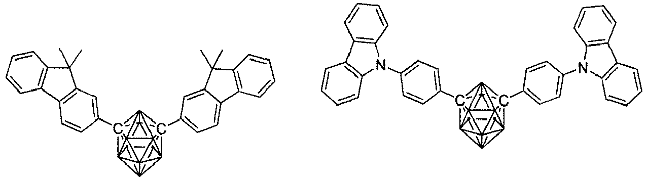

- In order to apply an organic EL device to a display device in a flat panel display or the like, it is necessary to improve the luminous efficacy of the device and also to ensure sufficiently the stability in driving the device. The present invention has an object to provide, in view of the above-mentioned circumstances, an organic EL device that has high efficiency and high driving stability and is practically useful and a compound suitable for the organic EL device.
- The inventors of the present invention have made intensive investigations and have consequently found that, when a carborane compound in which at least one dibenzofuranyl group is bonded is used in an organic EL device, the organic EL device exhibits excellent characteristics. As a result, the present invention has been completed.
- The present invention relates to a material for an organic electroluminescent device, including a carborane compound represented by the following general formula (1).


- In the general formula (1):
- a ring A represents a divalent carborane group C2B10H10 represented by the formula (1a) or the formula (1b), and when the plurality of rings A are present in a molecule thereof, the rings may be identical to or different from each other;
- s represents a number of repetitions and represents an integer of from 1 to 4, and n and m each represent a substitution number, n represents an integer of from 0 to 4 and m represents an integer of from 0 to 4, provided that when n=1, s=1;
- L1 represents an n+1-valent substituted or unsubstituted aromatic hydrocarbon group having 6 to 30 carbon atoms, an n+1-valent substituted or unsubstituted aromatic heterocyclic group having 3 to 30 carbon atoms, or an n+1-valent linked aromatic group formed by linking 2 to 6 aromatic rings of the aromatic hydrocarbon group or the aromatic heterocyclic group, and when n=1, L1 represents a group containing at least one aromatic heterocyclic group or a single bond;
- L2 represents a single bond, a divalent substituted or unsubstituted aromatic hydrocarbon group having 6 to 30 carbon atoms, a divalent substituted or unsubstituted aromatic heterocyclic group having 3 to 30 carbon atoms, or a divalent linked aromatic group formed by linking 2 to 6 aromatic rings of the aromatic hydrocarbon group or the aromatic heterocyclic group, and terminal L2-H may be an alkyl group having 1 to 12 carbon atoms, an alkoxy group having 1 to 12 carbon atoms, or an acetyl group;
- R represents an alkyl group having 1 to 12 carbon atoms, an alkoxy group having 1 to 12 carbon atoms, an acetyl group, a substituted or unsubstituted aromatic hydrocarbon group having 6 to 30 carbon atoms, a substituted or unsubstituted aromatic heterocyclic group having 3 to 30 carbon atoms, or a linked aromatic group formed by linking 2 to 6 aromatic rings of the aromatic hydrocarbon group or the aromatic heterocyclic group;
- when L1, L2, or R represents a linked aromatic group, the group may be linear or branched, and the aromatic rings to be linked may be identical to or different from each other; and
- when a plurality of s's, L2's, or R's are present in the molecule, the plurality of s's, L2's, or R's may be identical to or different from each other.
- In the general formula (1), it is preferred that any one or more of the following (1) to (4) be satisfied:
- (1) n represents an integer of 0 or 1;
- (2) the ring A represents a divalent carborane group C2B10H10 represented by the formula (1a);
- (3) L1 and L2 each independently represent a substituted or unsubstituted aromatic hydrocarbon group having 6 to 18 carbon atoms, a substituted or unsubstituted aromatic heterocyclic group having 3 to 17 carbon atoms, or a linked aromatic group formed by linking 2 to 6 aromatic rings selected from the aromatic hydrocarbon group and the aromatic heterocyclic group;
- (4) L1 and L2 each independently represent a substituted or unsubstituted aromatic heterocyclic group having 3 to 30 carbon atoms, or a linked aromatic group formed by linking 2 to 6 aromatic rings selected from the aromatic heterocyclic group.
- Part or the entirety of hydrogen atoms in the carborane compound represented by the general formula (1) may each be substituted with deuterium.
- The present invention also relates to an organic electroluminescent device having a structure in which an anode, an organic layer, and a cathode are laminated on a substrate, in which the organic layer includes an organic layer containing the above-mentioned material for an organic electroluminescent device.
- It is preferred that the organic layer containing the material for an organic electroluminescent device include at least one layer selected from the group consisting of a light-emitting layer, an electron-transporting layer, and a hole-blocking layer, or include a light-emitting layer containing a phosphorescent light-emitting dopant. When the phosphorescent light-emitting dopant is contained, it is preferred that its emission wavelength have an emission maximum wavelength at 550 nm or less.
- A material for a phosphorescent device of the present invention has a structure in which at least one dibenzofuranyl group is bonded onto a carborane skeleton. A carborane compound having such structural feature enables high-level control of the electron-injecting/transporting properties because its lowest unoccupied molecular orbital (LUMO) that affects the electron-injecting/transporting properties is widely distributed in the entirety of a molecule thereof. Further, the compound enables efficient light emission from a dopant because that its triplet excitation energy (T1 energy) is enough high to confine the T1 energy of the dopant. By virtue of the foregoing features, the organic EL device which contains the compound can achieve low voltage and high luminous efficacy respectively.
- In addition, the material for an organic electroluminescent device of the present invention shows a satisfactory amorphous characteristic and high heat stability, and at the same time, is extremely stable in an excited state. Accordingly, an organic EL device using the material has a long driving lifetime and durability at a practical level.
-
-
FIG. 1 is a sectional view for illustrating an example of the structure of an organic EL device. -
FIG. 2 is an NMR chart of acarborane compound 1 of the present invention. - A material for an organic electroluminescent device of the present invention is a carborane compound represented by the general formula (1). The carborane compound exhibits such excellent effects as described above probably because the compound has a structure in which at least one dibenzofuranyl group is bonded.
- L1 represents an n+1-valent substituted or unsubstituted aromatic hydrocarbon group having 6 to 30 carbon atoms, an n+1-valent substituted or unsubstituted aromatic heterocyclic group having 3 to 30 carbon atoms, or an n+1-valent linked aromatic group formed by linking 2 to 6 aromatic rings of the aromatic hydrocarbon group or the aromatic heterocyclic group. When L1 represents the linked aromatic group, the group may be linear or branched, and the aromatic rings to be linked may be identical to or different from each other. The same holds true for the case where L2 or R represents a linked aromatic group.
- L2 represents a single bond, a divalent substituted or unsubstituted aromatic hydrocarbon group having 6 to 30 carbon atoms, a divalent substituted or unsubstituted aromatic heterocyclic group having 3 to 30 carbon atoms, or a divalent linked aromatic group formed by linking 2 to 6 aromatic rings of the aromatic hydrocarbon group or the aromatic heterocyclic group, and terminal L2-H may be an alkyl group having 1 to 12 carbon atoms, an alkoxy group having 1 to 12 carbon atoms, or an acetyl group.
- R represents an alkyl group having 1 to 12 carbon atoms, an alkoxy group having 1 to 12 carbon atoms, an acetyl group, a substituted or unsubstituted aromatic hydrocarbon group having 6 to 30 carbon atoms, a substituted or unsubstituted aromatic heterocyclic group having 3 to 30 carbon atoms, or a linked aromatic group formed by linking 2 to 6 aromatic rings of the aromatic hydrocarbon group or the aromatic heterocyclic group.
- The case where L1, L2, and R each represent an aromatic hydrocarbon group, an aromatic heterocyclic group, or a linked aromatic group is described. It should be noted that when L1, L2, and R each represent any such group, L1 represents an n+1-valent group, L2 represents a divalent group, and R represents a monovalent group.
- Specific examples of the unsubstituted aromatic hydrocarbon group include groups each produced by removing a hydrogen atom from an aromatic hydrocarbon compound, such as benzene, naphthalene, fluorene, anthracene, phenanthrene, triphenylene, tetraphenylene, fluoranthene, pyrene, or chrysene. Of those, a group produced by removing a hydrogen atom from benzene, naphthalene, fluorene, phenanthrene, or triphenylene is preferred.
- Specific examples of the unsubstituted aromatic heterocyclic group include linking groups each produced by removing a hydrogen atom from an aromatic heterocyclic compound, such as pyridine, pyrimidine, triazine, quinoline, isoquinoline, quinoxaline, naphthyridine, carbazole, dibenzofuran, acridine, azepine, tribenzazepine, phenazine, phenoxazine, phenothiazine, dibenzophosphole, or dibenzoborole. Of those, a group produced by removing a hydrogen atom from pyridine, pyrimidine, triazine, carbazole, or dibenzofuran is preferred.
- A group produced by removing a hydrogen atom from an aromatic compound in which a plurality of aromatic hydrocarbon compounds or aromatic heterocyclic compounds are linked to each other is referred to as "linked aromatic group. " The linked aromatic group is a group formed by linking 2 to 6 aromatic rings, the aromatic rings to be linked may be identical to or different from each other, and both an aromatic hydrocarbon group and an aromatic heterocyclic group may be included. The number of the aromatic rings to be linked is preferably from 2 to 4, more preferably 2 or 3.
- Specific examples of the linked aromatic group include groups each produced by removing a hydrogen atom from biphenyl, terphenyl, phenylnaphthalene, diphenylnaphthalene, phenylanthracene, diphenylanthracene, diphenylfluorene, bipyridine, bipyrimidine, bitriazine, biscarbazole, bisdibenzofuran, bisdibenzothiophene, phenylpyridine, phenylpyrimidine, phenyltriazine, phenylcarbazole, phenyldibenzofuran, diphenylpyridine, diphenyltriazine, bis(carbazolyl)benzene, bis(dibenzofuranyl)benzene, or the like.
- The aromatic hydrocarbon group, the aromatic heterocyclic group, or the linked aromatic group may have a substituent, and when any such group has a substituent, a preferred substituent is an alkyl group having 1 to 12 carbon atoms, an alkoxy group having 1 to 12 carbon atoms, or an acetyl group. Amore preferred substituent is an alkyl group having 1 to 4 carbon atoms, an alkoxy group having 1 or 2 carbon atoms, or an acetyl group.
- Here, when the linked aromatic group is a divalent group, the group is represented by, for example, any one of the following formulae, and its aromatic rings may be linked in a linear manner or a branched manner.


- In the general formula (1), s represents a number of repetitions and represents an integer of from 1 to 4, preferably an integer of 1 or 2.
- In the general formula (1), m and n each represent a substitution number, n represents an integer of from 0 to 4, and m represents an integer of from 1 to 4. It is preferred that n represent an integer of 0 or 1 and m represent an integer of 1 or 2.
- The case where R and terminal L2-H each represent an alkyl group or an alkoxy group is described.
- The alkyl group may be saturated or unsaturated, and may be linear, branched, or cyclic. Preferred specific examples thereof include: alkyl groups each having 1 to 8 carbon atoms, such as a methyl group, an ethyl group, an ethenyl group, a propyl group, a propenyl group, an isopropyl group, a butyl group, a t-butyl group, a pentyl group, a hexyl group, and an octyl group; and cycloalkyl groups each having 5 to 8 carbon atoms, such as a cyclopentyl group and a cyclohexyl group.
- The alkoxy group may be linear or branched. Preferred specific examples thereof include alkoxy groups each having 1 to 8 carbon atoms, such as a methoxy group, an ethoxy group, a propoxy group, an isopropoxy group, a butoxy group, a t-butoxy group, a pentoxy group, a 2-ethylbutoxy group, a hexyloxy group, and an octyloxy group.
- In the general formula (1), a ring A represents a divalent carborane group C2B10H10 represented by the formula (1a) or (1b). The two bonding hands of the divalent carborane group may each be produced from C or may each be produced from B, but a bonding hand to be bonded to L1 or L2 is preferably produced from C. Of the divalent carborane groups, a carborane group represented by the formula (1a) is preferred.
- The carborane compound represented by the general formula (1) can be synthesized from raw materials selected in accordance with the structure of the target compound by using a known approach.
- (A-1) can be synthesized through the following reaction formula with reference to a synthesis example described in Journal of Organometallic Chemistry, 1993, 462, p19-29.

- Specific examples of the carborane compound represented by the general formula (1) are shown below. However, the material for an organic electroluminescent device of the present invention is not limited thereto.

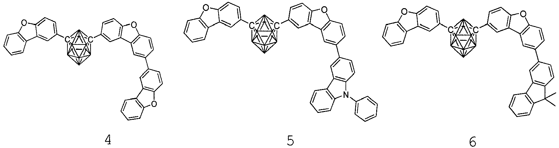


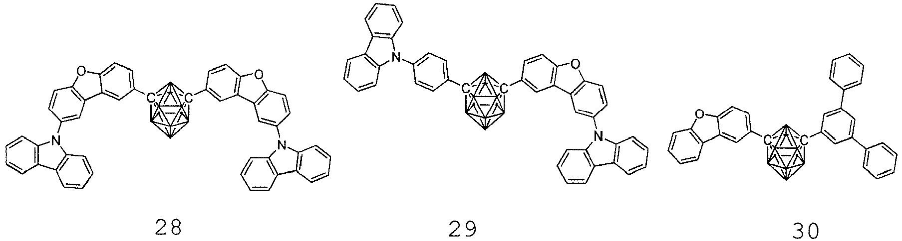


- When the material for an organic electroluminescent device of the present invention (sometimes referred to as compound of the present invention, compound represented by the general formula (1), or carborane compound) is contained in at least one of a plurality of organic layers of an organic EL device having a structure in which an anode, the plurality of organic layers, and a cathode are laminated on a substrate, an excellent organic electroluminescent device is provided. A light-emitting layer, an electron-transporting layer, or a hole-blocking layer is suitable as the organic layer in which the compound of the present invention is contained. Here, when the compound of the present invention is used in the light-emitting layer, the compound can be used as a host material for the light-emitting layer containing a fluorescent light-emitting, delayed fluorescent light-emitting, or phosphorescent light-emitting dopant. In addition, the compound of the present invention can be used as an organic light-emitting material that radiates fluorescence and delayed fluorescence. When the compound of the present invention is used as an organic light-emitting material that radiates fluorescence and delayed fluorescence, any other organic compound having a value for at least one of excited singlet energy or excited triplet energy higher than that of the compound is preferably used as the host material. The compound of the present invention is particularly preferably incorporated as a host material for the light-emitting layer containing the phosphorescent light-emitting dopant.
- Next, an organic EL device using the material for an organic electroluminescent device of the present invention is described.
- The organic EL device of the present invention includes organic layers including at least one light-emitting layer between an anode and a cathode laminated on a substrate. In addition, at least one of the organic layers contains the material for an organic electroluminescent device of the present invention. The material for an organic electroluminescent device of the present invention is advantageously contained in the light-emitting layer together with a phosphorescent light-emitting dopant.
- Next, the structure of the organic EL device of the present invention is described with reference to the drawings. However, the structure of the organic EL device of the present invention is by no means limited to one illustrated in the drawings.
-
FIG. 1 is a sectional view for illustrating an example of the structure of a general organic EL device used in the present invention.Reference numeral 1 represents a substrate,reference numeral 2 represents an anode,reference numeral 3 represents a hole-injecting layer,reference numeral 4 represents a hole-transporting layer,reference numeral 5 represents a light-emitting layer,reference numeral 6 represents an electron-transporting layer, and reference numeral 7 represents a cathode. The organic EL device of the present invention may include an exciton-blocking layer adjacent to the light-emitting layer, or may include an electron-blocking layer between the light-emitting layer and the hole-injecting layer. The exciton-blocking layer may be inserted on any of the anode side and the cathode side of the light-emitting layer, and may also be inserted simultaneously on both sides. The organic EL device of the present invention includes the substrate, the anode, the light-emitting layer, and the cathode as its essential layers. The organic EL device of the present invention preferably includes a hole-injecting/transporting layer and an electron-injecting/transporting layer in addition to the essential layers, and more preferably includes a hole-blocking layer between the light-emitting layer and the electron-injecting/transporting layer. It should be noted that the hole-injecting/transporting layer means any one or both of the hole-injecting layer and the hole-transporting layer, and that the electron-injecting/transporting layer means any one or both of an electron-injecting layer and the electron-transporting layer. - It should be noted that it is possible to adopt a reverse structure as compared to
FIG. 1 , that is, the reverse structure being formed by laminating the layers on thesubstrate 1 in the order of the cathode 7, the electron-transportinglayer 6, the light-emittinglayer 5, the hole-transportinglayer 4, and theanode 2. In this case as well, some layers may be added or eliminated as required. - The organic EL device of the present invention is preferably supported by a substrate. The substrate is not particularly limited, and any substrate that has long been conventionally used for an organic EL device may be used. For example, a substrate made of glass, a transparent plastic, quartz, or the like may be used.
- Preferably used as the anode in the organic EL device is an anode formed by using, as an electrode substance, any of a metal, an alloy, an electrically conductive compound, and a mixture thereof, all of which have a large work function (4 eV or more). Specific examples of such electrode substance include metals such as Au and conductive transparent materials such as CuI, indium tin oxide (ITO), SnO2, and ZnO. In addition, a material such as IDIXO (In2O3-ZnO), which can produce an amorphous, transparent conductive film, may be used. In order to produce the anode, it may be possible to form any of those electrode substances into a thin film by using a method such as vapor deposition or sputtering and form a pattern having a desired shape thereon by photolithography. Alternatively, in the case of not requiring high pattern accuracy (about 100 µm or more), a pattern may be formed via a mask having a desired shape when any of the above-mentioned electrode substances is subjected to vapor deposition or sputtering. Alternatively, when a coatable substance, such as an organic conductive compound, is used, a wet film-forming method, such as a printing method or a coating method, may be used. When luminescence is taken out from the anode, the transmittance of the anode is desirably controlled to more than 10%. In addition, the sheet resistance of the anode is preferably several hundred ohms per square (Ω/□) or less. Further, the thickness of the film is, depending on its material, selected from the range of generally from 10 nm to 1,000 nm, preferably from 10 nm to 200 nm.
- On the other hand, used as the cathode is a cathode formed by using, as an electrode substance, any of a metal (referred to as electron-injecting metal), an alloy, an electrically conductive compound, and a mixture thereof, all of which have a small work function (4 eV or less). Specific examples of such electrode substance include sodium, a sodium-potassium alloy, magnesium, lithium, a magnesium/copper mixture, a magnesium/silver mixture, a magnesium/aluminum mixture, a magnesium/indium mixture, an aluminum/aluminum oxide (Al2O3) mixture, indium, a lithium/aluminum mixture, and a rare earth metal. Of those, for example, a mixture of an electron-injecting metal and a second metal, which is a stable metal having a larger work function value than the former metal, such as a magnesium/silver mixture, a magnesium/aluminum mixture, a magnesium/indium mixture, an aluminum/aluminum oxide (Al2O3) mixture, or a lithium/aluminum mixture, or aluminum, is suitable from the viewpoints of an electron-inj ecting property and durability against oxidation or the like. The cathode can be produced by forming any of those electrode substances into a thin film by using a method such as vapor deposition or sputtering. In addition, the sheet resistance of the cathode is preferably several hundred Ω/□ or less, and the thickness of the film is selected from the range of generally from 10 nm to 5 µm, preferably from 50 nm to 200 nm. It should be noted that, in order for luminescence produced to pass through, any one of the anode and cathode of the organic EL device is preferably transparent or semi-transparent, because the light emission luminance improves.
- In addition, after the above-mentioned metal has been formed into a film having a thickness of from 1 nm to 20 nm as a cathode, the conductive transparent material mentioned in the description of the anode is formed into a film on the cathode, thereby being able to produce a transparent or semi-transparent cathode. Through the application of this, a device in which both the anode and cathode have transparency can be produced.
- The light-emitting layer is a layer that emits light after the production of an exciton by the recombination of a hole injected from the anode and an electron injected from the cathode, and the light-emitting layer contains an organic light-emitting material and a host material.
- When the light-emitting layer is a fluorescent light-emitting layer, at least one kind of fluorescent light-emitting material may be used alone as the fluorescent light-emitting material. However, it is preferred that the fluorescent light-emitting material be used as a fluorescent light-emitting dopant and the host material be contained.
- The carborane compound represented by the general formula (1) can be used as the fluorescent light-emitting material in the light-emitting layer. However, the fluorescent light-emitting material is known through, for example, many patent literatures, and hence can be selected therefrom. Examples thereof include a benzoxazole derivative, a benzothiazole derivative, a benzimidazole derivative, a styrylbenzene derivative, a polyphenyl derivative, a diphenylbutadiene derivative, a tetraphenylbutadiene derivative, a naphthalimide derivative, a coumarin derivative, a fused aromatic compound, a perinone derivative, an oxadiazole derivative, an oxazine derivative, an aldazine derivative, a pyrrolidine derivative, a cyclopentadiene derivative, a bisstyrylanthracene derivative, a quinacridone derivative, a pyrrolopyridine derivative, a thiadiazolopyridine derivative, a styrylamine derivative, a diketopyrrolopyrrole derivative, an aromatic dimethylidene compound, various metal complexes typified by a metal complex of a 8-quinolinol derivative, and a metal complex, rare earth complex, or transition metal complex of a pyrromethene derivative, polymer compounds such as polythiophene, polyphenylene, and polyphenylene vinylene, and an organic silane derivative. Of those, for example, the following compound is preferred: a fused aromatic compound, a styryl compound, a diketopyrrolopyrrole compound, an oxazine compound, or a pyrromethene metal complex, transition metal complex, or lanthanoid complex. For example, the following compound is more preferred: naphthacene, pyrene, chrysene, triphenylene, benzo[c]phenanthrene, benzo[a]anthracene, pentacene, perylene, fluoranthene, acenaphthofluoranthene, dibenzo[a,j]anthracene, dibenzo[a,h]anthracene, benzo[a]naphthacene, hexacene, anthanthrene, naphtho[2,1-f]isoquinoline, α-naphthaphenanthridine, phenanthroxazole, quinolino[6,5-f]quinoline, or benzothiophanthrene. Those compounds may each have an alkyl group, aryl group, aromatic heterocyclic group, or diarylamino group as a substituent.
- The carborane compound represented by the general formula (1) can be used as a fluorescent host material in the light-emitting layer. However, the fluorescent host material is known through, for example, many patent literatures, and hence can be selected therefrom. For example, the following material can be used: a compound having a fused aryl ring, such as naphthalene, anthracene, phenanthrene, pyrene, chrysene, naphthacene, triphenylene, perylene, fluoranthene, fluorene, or indene, or a derivative thereof; an aromatic amine derivative, such as N,N'-dinaphthyl-N,N'-diphenyl-4,4'-diphenyl-1,1'-diamine; a metal chelated oxinoid compound typified by tris(8-quinolinato)aluminum(III); a bisstyryl derivative, such as a distyrylbenzene derivative; a tetraphenylbutadiene derivative; an indene derivative; a coumarin derivative; an oxadiazole derivative; a pyrrolopyridine derivative; a perinone derivative; a cyclopentadiene derivative; a pyrrolopyrrole derivative; a thiadiazolopyridine derivative; a dibenzofuran derivative; a carbazole derivative; an indolocarbazole derivative; a triazine derivative; or a polymer-based derivative, such as a polyphenylene vinylene derivative, a poly-p-phenylene derivative, a polyfluorene derivative, a polyvinyl carbazole derivative, or a polythiophene derivative. However, the fluorescent host material is not particularly limited thereto.
- When the fluorescent light-emitting material is used as a fluorescent light-emitting dopant and the host material is contained, the content of the fluorescent light-emitting dopant in the light-emitting layer desirably falls within the range of from 0.01 wt% to 20 wt%, preferably from 0.1 wt% to 10 wt%.
- An organic EL device typically injects charges from both of its electrodes, i.e. , its anode and cathode into a light-emitting substance to produce a light-emitting substance in an excited state, and causes the substance to emit light. In the case of a charge injection-type organic EL device, it is said that 25% of the produced excitons are excited to a singlet excited state and the remaining 75% of the excitons are excited to a triplet excited state. As described in Advanced Materials 2009, 21, 4802-4806., it has been known that after a specific fluorescent light-emitting substance has undergone an energy transition to a triplet excited state as a result of intersystem crossing or the like, the substance is subjected to inverse intersystem crossing to a singlet excited state by triplet-triplet annihilation or the absorption of thermal energy to radiate fluorescence, thereby expressing thermally activated delayed fluorescence. The organic EL device of the present invention can also express delayed fluorescence. In this case, the light emission can include both fluorescent light emission and delayed fluorescent light emission. It should be noted that light emission from the host material may be present in part of the light emission.
- When the light-emitting layer is a delayed fluorescent light-emitting layer, at least one kind of delayed fluorescent light-emitting material may be used alone as a delayed fluorescent light-emitting material. However, it is preferred that the delayed fluorescent light-emittingmaterial be used as a delayed fluorescent light-emitting dopant and the host material be contained.
- Although the carborane compound represented by the general formula (1) can be used as the delayed fluorescent light-emitting material in the light-emitting layer, a material selected from known delayed fluorescent light-emitting materials can also be used. Examples thereof include a tin complex, an indolocarbazole derivative, a copper complex, and a carbazole derivative. Specific examples thereof include, but not limited to, compounds described in the following non patent literatures and patent literature.
- (1) Adv. Mater. 2009, 21, 4802-4806, (2) Appl. Phys. Lett. 98, 083302 (2011), (3)
JP 2011-213643 A - Specific examples of the delayed fluorescent light-emitting material are shown below, but the delayed fluorescent light-emitting material is not limited to the following compounds.


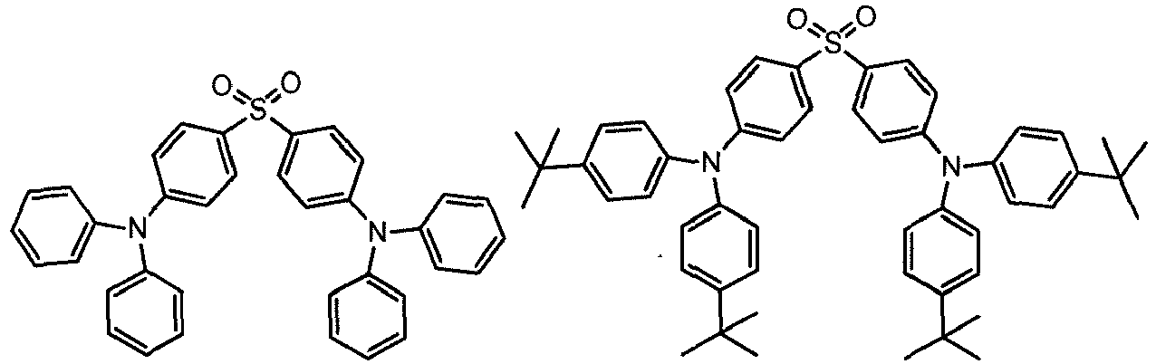
- When the delayed fluorescent light-emitting material is used as a delayed fluorescent light-emitting dopant and the host material is contained, the content of the delayed fluorescent light-emitting dopant in the light-emitting layer desirably falls within the range of from 0.01 wt% to 50 wt%, preferably from 0.1 wt% to 20 wt%, more preferably from 0.01 wt% to 10%.
- The carborane compound represented by the general formula (1) can be used as the delayed fluorescent host material in the light-emitting layer. However, the delayed fluorescent host material can also be selected from compounds except the carborane. For example, the following compound can be used: a compound having a fused aryl ring, such as naphthalene, anthracene, phenanthrene, pyrene, chrysene, naphthacene, triphenylene, perylene, fluoranthene, fluorene, or indene, or a derivative thereof; an aromatic amine derivative, such as N,N'-dinaphthyl-N,N'-diphenyl-4,4'-diphenyl-1,1'-diamine; a metal chelated oxinoid compound typified by tris(8-quinolinato)aluminum(III); a bisstyryl derivative, such as a distyrylbenzene derivative; a tetraphenylbutadiene derivative; an indene derivative; a coumarin derivative; an oxadiazole derivative; a pyrrolopyridine derivative; a perinone derivative; a cyclopentadiene derivative; a pyrrolopyrrole derivative; a thiadiazolopyridine derivative; a dibenzofuran derivative; a carbazole derivative; an indolocarbazole derivative; a triazine derivative; or a polymer-based derivative, such as a polyphenylene vinylene derivative, a poly-p-phenylene derivative, a polyfluorene derivative, a polyvinyl carbazole derivative, a polythiophene derivative, or an arylsilane derivative. However, the delayed fluorescent host material is not particularly limited thereto.
- When the light-emitting layer is a phosphorescent light-emitting layer, the light-emitting layer contains a phosphorescent light-emitting dopant and a host material. It is recommended to use, as a material for the phosphorescent light-emitting dopant, a material containing an organic metal complex including at least one metal selected from ruthenium, rhodium, palladium, silver, rhenium, osmium, iridium, platinum, and gold.
- Preferred examples of the phosphorescent light-emitting dopant include complexes such as Ir(ppy)3, complexes such as Ir(bt)2·acac3, and complexes such as PtOEt3, the complexes each having a noble metal element, such as Ir, as a central metal. Specific examples of those complexes are shown below, but the complexes are not limited to the compounds described below.


- It is desired that the content of the phosphorescent light-emitting dopant in the light-emitting layer fall within the range of from 2 wt% to 40 wt%, preferably from 5 wt% to 30 wt%.
- When the light-emitting layer is a phosphorescent light-emitting layer, it is preferred to use, as a host material in the light-emitting layer, the carborane compound of the present invention. However, when the carborane compound is used in any other organic layer except the light-emitting layer, the material to be used in the light-emitting layer may be another host material except the carborane compound, or the carborane compound and any other host material may be used in combination. Further, a plurality of kinds of known host materials may be used in combination.
- It is preferred to use, as a usable known host compound, a compound that has a hole-transporting ability or an electron-transporting ability, is capable of preventing luminescence from having a longer wavelength, and has a high glass transition temperature.
- Any such other host material is known through, for example, many patent literatures, and hence can be selected therefrom. Specific examples of the host material include, but are not particularly limited to, an indole derivative, a carbazole derivative, a triazole derivative, an oxazole derivative, an oxadiazole derivative, an imidazole derivative, a polyarylalkane derivative, a pyrazoline derivative, a pyrazolone derivative, a phenylenediamine derivative, an arylamine derivative, an amino-substituted chalcone derivative, a styrylanthracene derivative, a fluorenone derivative, a hydrazone derivative, a stilbene derivative, a silazane derivative, an aromatic tertiary amine compound, a styrylamine compound, an aromatic dimethylidene-based compound, a porphyrin-based compound, an anthraquinodimethane derivative, an anthrone derivative, a diphenylquinone derivative, a thiopyran dioxide derivative, a heterocyclic tetracarboxylic acid anhydride, such as naphthalene perylene, a phthalocyanine derivative, various metal complexes typified by a metal complex of an 8-quinolinol derivative, a metal phthalocyanine, and metal complexes of benzoxazole and benzothiazole derivatives, and polymer compounds, such as a polysilane-based compound, a poly(N-vinylcarbazole) derivative, an aniline-based copolymer, a thiophene oligomer, a polythiophene derivative, a polyphenylene derivative, a polyphenylenevinylene derivative, and a polyfluorene derivative.
- The light-emitting layer, which may be any one of a fluorescent light-emitting layer, a delayed fluorescent light-emitting layer, and a phosphorescent light-emitting layer, is preferably the phosphorescent light-emitting layer.
- The injecting layer refers to a layer formed between an electrode and an organic layer for the purposes of lowering a driving voltage and improving light emission luminance, and includes a hole-injecting layer and an electron-injecting layer. The injecting layer may be interposed between the anode and the light-emitting layer or the hole-transporting layer, or may be interposed between the cathode and the light-emitting layer or the electron-transporting layer. The injecting layer may be formed as required.
- The hole-blocking layer has, in a broad sense, the function of an electron-transporting layer, and is formed of a hole-blocking material that has a remarkably small ability to transport holes while having a function of transporting electrons, and hence the hole-blocking layer is capable of improving the probability of recombining an electron and a hole by blocking holes while transporting electrons.
- It is preferred to use the carborane compound represented by the general formula (1) according to the present invention for the hole-blocking layer. However, when the carborane compound is used in any other organic layer, a known material for a hole-blocking layer may be used. In addition, a material for the electron-transporting layer to be described later can be used as a material for the hole-blocking layer as required.
- The electron-blocking layer is formed of a material that has a remarkably small ability to transport electrons while having a function of transporting holes, and hence the electron-blocking layer is capable of improving the probability of recombining an electron and a hole by blocking electrons while transporting holes.
- A material for the hole-transporting layer to be described later can be used as a material for the electron-blocking layer as required. The thickness of the electron-blocking layer is preferably from 3 nm to 100 nm, more preferably from 5 nm to 30 nm.
- The exciton-blocking layer refers to a layer for blocking excitons produced by the recombination of a hole and an electron in the light-emitting layer from diffusing into charge-transporting layers. The insertion of this layer enables efficient confinement of the excitons in the light-emitting layer, thereby being able to improve the luminous efficacy of the device. The exciton-blocking layer can be inserted on any of the anode side and the cathode side of the adjacent light-emitting layer, and can also be inserted simultaneously on both sides.
- Although the carborane compound represented by the general formula (1) can be used as a material for the exciton-blocking layer, as other materials therefor, there are given, for example, 1,3-dicarbazolylbenzene (mCP) and bis(2-methyl-8-quinolinolato)-4-phenylphenolatoaluminum(III) (BAlq).
- The hole-transporting layer is formed of a hole-transporting material having a function of transporting holes, and a single hole-transporting layer or a plurality of hole-transporting layers can be formed.
- The hole-transporting material has a hole-injecting property or a hole-transporting property or has an electron-blocking property, and any of an organic material and an inorganic material can be used as the hole-transporting material. Although it is preferred to use the carborane compound represented by the general formula (1) as a known hole-transporting material that can be used, any compound selected from conventionally known compounds can be used. Examples of the known hole-transporting material that can be used include a triazole derivative, an oxadiazole derivative an imidazole derivative, a polyarylalkane derivative, a pyrazoline derivative, and a pyrazolone derivative, a phenylenediamine derivative, an arylamine derivative, an amino-substituted chalcone derivative, an oxazole derivative, a styrylanthracene derivative, a fluorenone derivative, a hydrazone derivative, a stilbene derivative, a silazane derivative, an aniline-based copolymer, and a conductive high-molecular weight oligomer, in particular, a thiophene oligomer. However, a porphyrin compound, an aromatic tertiary amine compound, or a styrylamine compound is preferably used, and an aromatic tertiary amine compound is more preferably used.
- The electron-transporting layer is formed of a material having a function of transporting electrons, and a single electron-transporting layer or a plurality of electron-transporting layers can be formed.
- An electron-transporting material (which also serves as a hole-blocking material in some cases) only needs to have a function of transferring electrons injected from the cathode into the light-emitting layer. Although it is preferred to use the carborane compound of the present invention for the electron-transporting layer, any compound selected from conventionally known compounds can be used. Examples thereof include a nitro-substituted fluorene derivative, a diphenylquinone derivative, a thiopyran dioxide derivative, a carbodiimide, a fluorenylidenemethane derivative, anthraquinodimethane, an anthrone derivative, and an oxadiazole derivative. Further, a thiadiazole derivative prepared by substituting an oxygen atom on an oxadiazole ring with a sulfur atom in the oxadiazole derivative or a quinoxaline derivative that has a quinoxaline ring known as an electron withdrawing group can be used as the electron-transporting material. Further, a polymer material in which any such material is introduced in a polymer chain or is used as a polymer main chain can be used.
- Now, the present invention is described in more detail by way of Examples. It should be appreciated that the present invention is not limited to Examples below and can be carried out in various forms as long as the various forms do not deviate from the gist of the present invention.
- The route described below was used to synthesize a carborane compound to be used as a material for an organic electroluminescent device. It should be noted that the number of each compound corresponds to the number given to the chemical formula.
- A
compound 1 is synthesized in accordance with the following reaction formulae.
- Under a nitrogen atmosphere, 35.0 g (0.243 mol) of m-carborane and 350 mL of 1,2-dimethoxyethane (DME) were added, and the resultant DME solution was cooled to 0°C. 96.8 mL of a 2.69 M solution of n-butyllithium in hexane was dropped to the solution, and the mixture was stirred under ice cooling for 30 minutes. 67 mL of pyridine was added to the resultant and the mixture was stirred at room temperature for 10 minutes. After that, 75.6 g (0.763 mol) of copper(I) chloride was added to the resultant and the mixture was stirred at 65°C for 30 minutes. After that, 76.4 g (0.260 mol) of 2-iododibenzofuran was added to the resultant and the mixture was stirred at 95°C overnight. The reaction solution was cooled to room temperature, and then the precipitated crystal was taken by filtration and the solvent was distilled off under reduced pressure. The resultant residue was purified by silica gel column chromatography to provide 25.0 g (3.22 mmol, 33% yield) of an intermediate A.
- Under a nitrogen atmosphere, 30.0 g (0.07 mol) of 2,8-diiododibenzofuran, 11. 9 g (0.07 mol) of carbazole, 1.33 g (7.0 mmol) of copper iodide, 44.6 g (0.21 mol) of tripotassium phosphate, 2.4 g (21.0 mmol) of trans-1,2-cyclohexanediamine, and 1 L of 1, 4-dioxane were added, and the mixture was stirred at 115 °C overnight. The reaction solution was cooled to room temperature, and then the precipitated crystal was taken by filtration and the solvent was distilled off under reduced pressure. The resultant residue was purified by silica gel column chromatography to provide 14.9 g (2.17 mmol, 47% yield) of an intermediate B as a white solid.
- Under a nitrogen atmosphere, 8.8 g (0.0285 mol) of the intermediate A and 63.0 mL of 1,2-dimethoxyethane (DME) were added, and the resultant DME solution was cooled to 0°C. 11.3 mL of a 2.69 M solution of n-butyllithium in hexane was dropped to the solution, and the mixture was stirred under ice cooling for 30 minutes. 7.8 mL of pyridine was added to the resultant and the mixture was stirred at room temperature for 10 minutes. After that, 8.7 g (88.4 mmol) of copper(I) chloride was added to the resultant and the mixture was stirred at 65°C for 30 minutes. After that, 14.0 g (0.0305 mol) of the intermediate B was added to the resultant and the mixture was stirred at 95°C for 4 days. The reaction solution was cooled to room temperature, and then the precipitated crystal was taken by filtration and the solvent was distilled off under reduced pressure. The resultant residue was purified by silica gel column chromatography to provide 3.0 g (4.67 mmol, 16% yield) of a
compound 1. APCI-TOFMS, m/z 642 [M+H]+. The measurement result of 1H-NMR (measurement solvent: CDCl3) is shown inFIG. 2 . - Compounds 13, 25, 26, 29, and 36 were synthesized in conformity with the synthesis example. In addition, compounds H-1 and H-2 for comparison were synthesized.


- Each thin film was laminated by a vacuum deposition method at a degree of vacuum of 2.0×10⁻⁵ Pa on a glass substrate on which an anode formed of indium tin oxide (ITO) having a thickness of 70 nmhadbeen formed. First, copper phthalocyanine (CuPC) was formed into a layer having a thickness of 30 nm to serve as a hole-injecting layer on the ITO. Next, diphenyl naphthyl diamine (NPD) was formed into a layer having a thickness of 15 nm to serve as a hole-transporting layer. Next, the
compound 1 serving as a host material for a light-emitting layer and an iridium complex [iridium(III) bis(4,6-di-fluorophenyl)-pyridinato-N,C2']picolinate] (FIrpic) serving as a blue phosphorescent material as a dopant were co-deposited from different deposition sources onto the hole-transporting layer to form a light-emitting layer having a thickness of 30 nm. The concentration of FIrpic was 20 %. Next, Alq3 was formed into a layer having a thickness of 25 nm to serve as an electron-transporting layer. Further, lithium fluoride (LiF) was formed into a layer having a thickness of 1.0 nm to serve as an electron-injecting layer on the electron-transporting layer. Finally, aluminum (Al) was formed into a layer having a thickness of 70 nm to serve as an electrode on the electron-injecting layer. The resultant organic EL device has such a layer construction that the electron-injecting layer is added between the cathode and the electron-transporting layer in the organic EL device illustrated inFIG. 1 . - An external power source was connected to the resultant organic EL device to apply a DC voltage to the device. As a result, it was confirmed that the device had such light-emitting characteristics as shown in Table 2. The columns "luminance", "voltage", and "luminous efficacy " in Table 1 show values at 2.5 mA/cm2 (initial characteristics). It should be noted that the maximum wavelength of the emission spectrum of the device was 475 nm, and hence the acquisition of light emission from FIrpic was found.
- Organic EL devices were each produced in the same manner as in Example 2 except that the compound 13, 25, 26, 29, or 36 was used instead of the
compound 1 as the host material for the light-emitting layer in Example 2. - An organic EL device was produced in the same manner as in Example 2 except that mCP was used as the host material for the light-emitting layer in Example 2.
- Organic EL devices were each produced in the same manner as in Example 2 except that the compound H-1 or H-2 was used as the host material for the light-emitting layer in Example 2.
- The organic EL devices obtained in Examples 2 to 7 and Comparative Examples 1 to 3 were evaluated in the same manner as in Example 3. As a result, it was confirmed that the devices had such light-emitting characteristics as shown in Table 1. It should be noted that the maximum wavelength of each of the emission spectra of the organic EL devices obtained in Examples 2 to 7 and Comparative Examples 1 to 3 was 475 nm, and hence the acquisition of light emission from FIrpic was identified.
[Table 1] Host material compound Luminance (cd/m2) Voltage (V) Visual luminous efficacy (lm/W) Example 2 1 200 7.3 3.4 Example 3 13 180 7.1 3.2 Example 4 25 210 7.4 3.6 Example 5 26 210 7.6 3.5 Example 6 29 190 7.6 3.1 Example 7 36 200 7.0 3.6 Comparative Example 1 mCP 140 8.7 2.0 Comparative Example 2 H-1 100 7.7 1.6 Comparative Example 3 H-2 140 7.5 2.4 - It is found from Table 1 that Examples 2 to 7 each using the carborane compound of the present invention in its light-emitting layer show characteristics better than those of Comparative Examples 1 to 4 in terms of luminous efficacy.
- Each thin film was laminated by a vacuum deposition method at a degree of vacuum of 2.0×10⁻⁵ Pa on a glass substrate on which an anode formed of indium tin oxide (ITO) having a thickness of 70 nmhadbeen formed. First, copperphthalocyanine (CuPC) was formed into a layer having a thickness of 30 nm to serve as a hole-injecting layer on the ITO. Next, diphenyl naphthyl diamine (NPD) was formed into a layer having a thickness of 15 nm to serve as a hole-transporting layer. Next, the
compound 1 serving as a host material for a light-emitting layer and Ir(ppy)3 serving as a dopant were co-deposited from different deposition sources onto the hole-transporting layer to form a light-emitting layer having a thickness of 30 nm. The concentration of Ir(ppy)3 was 10%. Next, Alq3 was formed into a layer having a thickness of 25 nm to serve as an electron-transporting layer. Further, lithium fluoride (LiF) was formed into a layer having a thickness of 1 nm to serve as an electron-injecting layer on the electron-transporting layer. Finally, aluminum (Al) was formed into a layer having a thickness of 70 nm to serve as an electrode on the electron-injecting layer. Thus, an organic EL device was produced. - An external power source was connected to the resultant organic EL device to apply a DC voltage to the device. As a result, it was confirmed that the device had such light-emitting characteristics as shown in Table 2. The columns "luminance", "voltage", and "luminous efficacy" in Table 2 show values at the time of driving at 20 mA/cm2 (initial characteristics). The maximum wavelength of the emission spectrum of the device was 530 nm, and hence the acquisition of light emission from Ir(ppy)3 was found.
- Organic EL devices were each produced in the same manner as in Example 7 except that the compound 13, 25, 26, 29, or 36 was used instead of the
compound 1 as the host material for the light-emitting layer in Example 10. - Organic EL devices were each produced in the same manner as in Example 8 except that CBP, H-1, or H-2 was used as the host material for the light-emitting layer in Example 8.
- The organic EL devices obtained in Examples and Comparative Examples above were evaluated in the same manner as in Example 8. As a result, it was confirmed that the devices had such light-emitting characteristics as shown in Table 2. It should be noted that the maximum wavelength of each of the emission spectra of the organic EL devices obtained in Examples and Comparative Examples above was 530 nm, and hence the acquisition of light emission from Ir(ppy)3 was identified.
[Table 2] Host material compound Luminance (cd/m2) Voltage (V) Visual luminous efficacy (lm/W) Example 8 1 2,000 8.5 3.7 Example 9 13 1,980 8.3 3.7 Example 10 25 2,100 8.6 3.8 Example 11 26 2,100 8.7 3.8 Example 12 29 1,980 8.7 3.6 Example 13 36 2,000 8.3 3.8 Comparative Example 4 CBP 1,120 8.7 2.0 Comparative Example 5 H-1 1,200 8.5 2.2 Comparative Example 6 H-2 1,000 8.3 1.9 - It is found from Table 2 that Examples 8 to 13 each using the carborane compound of the present invention in its light-emitting layer show characteristics better than those of Comparative Examples 4 to 6 in terms of luminous efficacy.
- Each thin film was laminated by a vacuum deposition method at a degree of vacuum of 2.0×10⁻⁵ Pa on a glass substrate on which an anode formed of indium tin oxide (ITO) having a thickness of 70 nmhadbeen formed. First, copperphthalocyanine (CuPC) was formed into a layer having a thickness of 30 nm to serve as a hole-injecting layer on the ITO. Next, diphenyl naphthyl diamine (NPD) was formed into a layer having a thickness of 15 nmto serve as a hole-transporting layer. Next, mCP serving as a host material for a light-emitting layer and FIrpic serving as a dopant were co-deposited from different deposition sources onto the hole-transporting layer to form a light-emitting layer having a thickness of 30 nm. The concentration of FIrpic was 20 wt%. Next, the
compound 1 was formed into a layer having a thickness of 5 nm to serve as a hole-blocking layer on the light-emitting layer. Next, Alq3 was formed into a layer having a thickness of 20 nm to serve as an electron-transporting layer. Further, lithium fluoride (LiF) was formed into a layer having a thickness of 1.0 nm to serve as an electron-inj ecting layer on the electron-transporting layer. Finally, aluminum (Al) was formed into a layer having a thickness of 70 nm to serve as an electrode on the electron-injecting layer. The resultant organic EL device has such a layer construction that the electron-injecting layer is added between the cathode and the electron-transporting layer and the hole-blocking layer is added between the light-emitting layer and the electron-transporting layer in the organic EL device illustrated inFIG. 1 . - An external power source was connected to the resultant organic EL device to apply a DC voltage to the device. As a result, it was confirmed that the device had such light-emitting characteristics as shown in Table 3. The columns "luminance", "voltage", and "luminous efficacy" in Table 3 show values at the time of driving at 20 mA/cm2. The maximum wavelength of the emission spectrum of the device was 475 nm, and hence the acquisition of light emission from FIrpic was found.
- Organic EL devices were each produced in the same manner as in Example 14 except that the compound 13, 25, 26, 29, or 36 was used instead of the
compound 1 as the hole-blocking material in Example 14. - An organic EL device was produced in the same manner as in Example 14 except that the thickness of Alq3 serving as the electron-transporting layer in Example 14 was changed to 25 nm and the hole-blocking layer was not formed.
- An organic EL device was produced in the same manner as in Example 14 except that the compound H-1 or H-2 was used as the hole-blocking material in Example 14.
- The organic EL devices obtained in Examples and Comparative Examples above were evaluated in the same manner as in Example 14. As a result, it was confirmed that the devices had such light-emitting characteristics as shown in Table 3. It should be noted that the maximum wavelength of each of the emission spectra of the organic EL devices obtained in Examples and Comparative Examples above was 475 nm, and hence the acquisition of light emission from FIrpic was identified. It should be noted that each of the host materials for the light-emitting layers used in Examples 15 to 19 and Comparative Examples 7 to 9 is mCP.
[Table 3] Hole-blocking material compound Luminance (cd/m2) Voltage (V) Visual luminous efficacy (lm/W) Example 14 1 210 8.0 3.3 Example 15 13 190 7.8 3.1 Example 16 25 195 8.0 3.1 Example 17 26 195 8.0 3.1 Example 18 29 200 8.0 3.1 Example 19 36 210 7.8 3.4 Comparative Example 7 - 140 - 8.7 2.0 Comparative Example 8 H-1 170 8.2 2.6 Comparative Example 9 H-2 180 8.3 2.7 - It is found from Table 3 that Examples 14 to 19 each using the carborane compound of the present invention in its hole-blocking layer show characteristics better than those of Comparative Example 7 not using the hole-blocking material and Comparative Examples 8 and 9 each using the other compound.
- 1 substrate, 2 anode, 3 hole-injecting layer, 4 hole-transporting layer, 5 light-emitting layer, 6 electron-transporting layer, 7 cathode
Claims (11)
- A material for an organic electroluminescent device, comprising a carborane compound represented by the general formula (1) :

 a ring A represents a divalent carborane group C2B10H10 represented by the formula (1a) or the formula (1b), and when the plurality of rings A are present in a molecule thereof, the rings may be identical to or different from each other, s represents a number of repetitions and represents an integer of from 1 to 4, and n and m each represent a substitution number, n represents an integer of from 0 to 4 and m represents an integer of from 0 to 4, provided that when n=1, s represents 1;L1 represents an n+1-valent substituted or unsubstituted aromatic hydrocarbon group having 6 to 30 carbon atoms, an n+1-valent substituted or unsubstituted aromatic heterocyclic group having 3 to 30 carbon atoms, or an n+1-valent linked aromatic group formed by linking 2 to 6 aromatic rings of the aromatic hydrocarbon group or the aromatic heterocyclic group, when L1 represents the linked aromatic group, the group may be linear or branched, and the aromatic rings to be linked may be identical to or different from each other, and when n=1, L1 represents a group containing at least one aromatic heterocyclic group or a single bond;L2 represents a single bond, a divalent substituted or unsubstituted aromatic hydrocarbon group having 6 to 30 carbon atoms, a divalent substituted or unsubstituted aromatic heterocyclic group having 3 to 30 carbon atoms, or a divalent linked aromatic group formed by linking 2 to 6 aromatic rings of the aromatic hydrocarbon group or the aromatic heterocyclic group, when L2 represents the linked aromatic group, the group may be linear or branched, and the aromatic rings to be linked may be identical to or different from each other, and terminal L2-H may be an alkyl group having 1 to 12 carbon atoms, an alkoxy group having 1 to 12 carbon atoms, or an acetyl group;R represents an alkyl group having 1 to 12 carbon atoms, an alkoxy group having 1 to 12 carbon atoms, an acetyl group, a substituted or unsubstituted aromatic hydrocarbon group having 6 to 30 carbon atoms, a substituted or unsubstituted aromatic heterocyclic group having 3 to 30 carbon atoms, or a linked aromatic group formed by linking 2 to 6 aromatic rings of the aromatic hydrocarbon group or the aromatic heterocyclic group, and when R represents the linked aromatic group, the group may be linear or branched, and the aromatic rings to be linked may be identical to or different from each other; andwhen a plurality of s's, L2's, or R's are present in the molecule, the plurality of s's, L2's, or R's may be identical to or different from each other.
 - A material for an organic electroluminescent device according to claim 1, wherein in the general formula (1), n represents 0 or 1.
- A material for an organic electroluminescent device according to claim 1, wherein in the general formula (1), the ring A represents a divalent carborane group C2B10H10 represented by the formula (1a).
- A material for an organic electroluminescent device according to claim 2, wherein in the general formula (1), the ring A represents a divalent carborane group C2B10H10 represented by the formula (1a).
- A material for an organic electroluminescent device according to claim 1, wherein in the general formula (1), L1 and L2 each independently represent a substituted or unsubstituted aromatic hydrocarbon group having 6 to 18 carbon atoms, a substituted or unsubstituted aromatic heterocyclic group having 3 to 17 carbon atoms, or a linked aromatic group formed by linking 2 to 6 aromatic rings selected from the aromatic hydrocarbon group and the aromatic heterocyclic group.
- A material for an organic electroluminescent device according to claim 1, wherein in the general formula (1), L1 and L2 each independently represent a substituted or unsubstituted aromatic heterocyclic group having 3 to 30 carbon atoms, or a linked aromatic group formed by linking 2 to 6 aromatic rings selected from the aromatic heterocyclic group.
- A material for an organic electroluminescent device according to claim 1, wherein in the general formula (1), n represents 0.
- An organic electroluminescent device having a structure in which an anode, an organic layer, and a cathode are laminated on a substrate, wherein the organic layer comprises an organic layer containing the material for an organic electroluminescent device of any one of claims 1 to 7.
- An organic electroluminescent device according to claim 8, wherein the organic layer containing the material for an organic electroluminescent device comprises at least one layer selected from the group consisting of a light-emitting layer, an electron-transporting layer, and a hole-blocking layer.
- An organic electroluminescent device according to claim 8, wherein the organic layer containing the material for an organic electroluminescent device is a light-emitting layer containing a phosphorescent light-emitting dopant.
- An organic electroluminescent device according to claim 10, wherein an emission wavelength of the phosphorescent light-emitting dopant has an emission maximum wavelength at 550 nm or less.
Applications Claiming Priority (4)
| Application Number | Priority Date | Filing Date | Title |
|---|---|---|---|
| JP2013204378 | 2013-09-30 | ||
| JP2013249413 | 2013-12-02 | ||
| JP2014071440 | 2014-03-31 | ||
| PCT/JP2014/072202 WO2015045705A1 (en) | 2013-09-30 | 2014-08-25 | Material for organic electroluminescent element and organic electroluminescent element using the same |
Publications (3)
| Publication Number | Publication Date |
|---|---|
| EP3054496A1 true EP3054496A1 (en) | 2016-08-10 |
| EP3054496A4 EP3054496A4 (en) | 2017-05-31 |
| EP3054496B1 EP3054496B1 (en) | 2018-01-31 |
Family
ID=52742857
Family Applications (1)
| Application Number | Title | Priority Date | Filing Date |
|---|---|---|---|
| EP14848256.5A Not-in-force EP3054496B1 (en) | 2013-09-30 | 2014-08-25 | Material for organic electroluminescent element and organic electroluminescent element using the same |
Country Status (7)
| Country | Link |
|---|---|
| US (1) | US10636981B2 (en) |
| EP (1) | EP3054496B1 (en) |
| JP (1) | JP6375302B2 (en) |
| KR (1) | KR102244235B1 (en) |
| CN (1) | CN105556695B (en) |
| TW (1) | TWI586664B (en) |
| WO (1) | WO2015045705A1 (en) |
Cited By (1)
| Publication number | Priority date | Publication date | Assignee | Title |
|---|---|---|---|---|
| EP3279962A4 (en) * | 2015-03-30 | 2018-08-08 | Nippon Steel & Sumikin Chemical Co., Ltd. | Material for organic electroluminescent element and organic electroluminescent element in which same is used |
Families Citing this family (10)
| Publication number | Priority date | Publication date | Assignee | Title |
|---|---|---|---|---|
| WO2015029796A1 (en) | 2013-08-29 | 2015-03-05 | Semiconductor Energy Laboratory Co., Ltd. | Heterocyclic compound, light-emitting element, light-emitting device, electronic device, and lighting device |
| JP6307332B2 (en) * | 2014-04-21 | 2018-04-04 | 新日鉄住金化学株式会社 | Organic electroluminescence device |
| JP2015227328A (en) * | 2014-05-02 | 2015-12-17 | 株式会社半導体エネルギー研究所 | COMPOUND, LIGHT EMITTING ELEMENT, LIGHT EMITTING DEVICE, ELECTRONIC DEVICE, AND LIGHTING DEVICE |
| EP3439058A4 (en) * | 2016-03-28 | 2019-11-13 | NIPPON STEEL Chemical & Material Co., Ltd. | ORGANIC ELECTROLUMINESCENT ELEMENT |
| CN108886105A (en) * | 2016-03-28 | 2018-11-23 | 新日铁住金化学株式会社 | Organic electroluminescence element |
| US10978647B2 (en) | 2017-02-15 | 2021-04-13 | Universal Display Corporation | Organic electroluminescent materials and devices |
| CN110431681B (en) * | 2017-03-23 | 2022-01-18 | 日铁化学材料株式会社 | Organic electroluminescent element |
| JPWO2019181465A1 (en) * | 2018-03-19 | 2021-04-30 | 日鉄ケミカル&マテリアル株式会社 | Organic electroluminescent device |
| CN113166089A (en) * | 2018-12-20 | 2021-07-23 | 默克专利有限公司 | Material for electronic devices |
| CN111662317B (en) * | 2020-07-09 | 2023-04-07 | 京东方科技集团股份有限公司 | Organic compound and organic electroluminescent device |
Family Cites Families (12)
| Publication number | Priority date | Publication date | Assignee | Title |
|---|---|---|---|---|
| WO2001041512A1 (en) | 1999-12-01 | 2001-06-07 | The Trustees Of Princeton University | Complexes of form l2mx as phosphorescent dopants for organic leds |
| JP2001313178A (en) | 2000-04-28 | 2001-11-09 | Pioneer Electronic Corp | Organic electroluminescence device |
| JP4387781B2 (en) | 2003-12-05 | 2009-12-24 | キヤノン株式会社 | Carborane compounds and conductive materials |
| JP4323935B2 (en) | 2003-12-05 | 2009-09-02 | キヤノン株式会社 | Organic light emitting device |
| JP2011213643A (en) | 2010-03-31 | 2011-10-27 | Canon Inc | Copper complex compound and organic luminescent element using the same |
| KR101881082B1 (en) * | 2011-06-20 | 2018-07-24 | 삼성디스플레이 주식회사 | Carborane compound, organic light-emitting diode comprising the same and flat display device |
| CN103988329B (en) * | 2011-12-12 | 2016-07-13 | 新日铁住金化学株式会社 | Material for organic electroluminescent element and organic electroluminescent element using same |
| JP5760282B2 (en) | 2011-12-19 | 2015-08-05 | ヨル チョン ケミカル カンパニーリミテッドYoul Chon Chemical Co., Ltd. | Novel compound having stability, charge transport material containing the same, and blue phosphorescent organic EL device |
| WO2014103910A1 (en) | 2012-12-26 | 2014-07-03 | 新日鉄住金化学株式会社 | Material for organic electroluminescent elements and organic electroluminescent elements using same |
| KR102111358B1 (en) * | 2012-12-26 | 2020-05-15 | 닛테츠 케미컬 앤드 머티리얼 가부시키가이샤 | Material for organic electroluminescent elements and organic electroluminescent element using same |
| CN107408639B (en) * | 2015-03-30 | 2019-11-22 | 日铁化学材料株式会社 | Material for organic electroluminescence element and organic electroluminescence element using the same |
| EP3439058A4 (en) * | 2016-03-28 | 2019-11-13 | NIPPON STEEL Chemical & Material Co., Ltd. | ORGANIC ELECTROLUMINESCENT ELEMENT |
-
2014
- 2014-08-25 US US14/909,461 patent/US10636981B2/en not_active Expired - Fee Related
- 2014-08-25 WO PCT/JP2014/072202 patent/WO2015045705A1/en not_active Ceased
- 2014-08-25 CN CN201480049987.4A patent/CN105556695B/en not_active Expired - Fee Related
- 2014-08-25 EP EP14848256.5A patent/EP3054496B1/en not_active Not-in-force
- 2014-08-25 KR KR1020167010953A patent/KR102244235B1/en not_active Expired - Fee Related
- 2014-08-25 JP JP2015539024A patent/JP6375302B2/en not_active Expired - Fee Related
- 2014-09-12 TW TW103131465A patent/TWI586664B/en not_active IP Right Cessation
Cited By (2)
| Publication number | Priority date | Publication date | Assignee | Title |
|---|---|---|---|---|
| EP3279962A4 (en) * | 2015-03-30 | 2018-08-08 | Nippon Steel & Sumikin Chemical Co., Ltd. | Material for organic electroluminescent element and organic electroluminescent element in which same is used |
| US10807996B2 (en) | 2015-03-30 | 2020-10-20 | Nippon Steel Chemical & Material Co., Ltd. | Material for organic electroluminescent element and organic electroluminescent element in which same is used |
Also Published As
| Publication number | Publication date |
|---|---|
| KR20160061406A (en) | 2016-05-31 |
| CN105556695B (en) | 2017-05-24 |
| US10636981B2 (en) | 2020-04-28 |
| JP6375302B2 (en) | 2018-08-15 |
| JPWO2015045705A1 (en) | 2017-03-09 |
| TWI586664B (en) | 2017-06-11 |
| EP3054496A4 (en) | 2017-05-31 |
| US20160190451A1 (en) | 2016-06-30 |
| EP3054496B1 (en) | 2018-01-31 |
| CN105556695A (en) | 2016-05-04 |
| TW201514169A (en) | 2015-04-16 |
| WO2015045705A1 (en) | 2015-04-02 |
| KR102244235B1 (en) | 2021-04-26 |
Similar Documents
| Publication | Publication Date | Title |
|---|---|---|
| EP2985802B1 (en) | Adamantane compound for organic electroluminescent elements, and organic electroluminescent element | |
| EP2793280B1 (en) | Organic electroluminescent element material and organic electroluminescent element using same | |
| EP2903048B1 (en) | Compound for organic electroluminescent elements, and organic electroluminescent element | |
| EP3054496B1 (en) | Material for organic electroluminescent element and organic electroluminescent element using the same | |
| EP3125326B1 (en) | Organic-electroluminescent-element material and organic electroluminescent elements using same | |
| EP3089230B1 (en) | Material for organic electroluminescent elements, and organic electroluminescent element using same | |
| EP3054495B1 (en) | Material for organic electroluminescent elements, and organic electroluminescent element using same | |
| KR20150100890A (en) | Material for organic electroluminescent elements and organic electroluminescent element using same | |
| US10468608B2 (en) | Organic-electroluminescent-element material, and organic electroluminescent element using same | |
| EP3125325B1 (en) | Organic-electroluminescent-element material and organic electroluminescent element using it | |
| EP3125324B1 (en) | Organic-electroluminescent-element material and organic electroluminescent element using same | |
| EP3089231B1 (en) | Material for organic electroluminescent elements, and organic electroluminescent element using same | |
| EP3279962B1 (en) | Material for organic electroluminescent element and organic electroluminescent element in which same is used |
Legal Events
| Date | Code | Title | Description |
|---|---|---|---|
| PUAI | Public reference made under article 153(3) epc to a published international application that has entered the european phase |
Free format text: ORIGINAL CODE: 0009012 |
|
| 17P | Request for examination filed |
Effective date: 20160303 |
|
| AK | Designated contracting states |
Kind code of ref document: A1 Designated state(s): AL AT BE BG CH CY CZ DE DK EE ES FI FR GB GR HR HU IE IS IT LI LT LU LV MC MK MT NL NO PL PT RO RS SE SI SK SM TR |
|
| AX | Request for extension of the european patent |
Extension state: BA ME |
|
| DAX | Request for extension of the european patent (deleted) | ||
| A4 | Supplementary search report drawn up and despatched |
Effective date: 20170502 |
|
| RIC1 | Information provided on ipc code assigned before grant |
Ipc: H05B 33/20 20060101ALI20170424BHEP Ipc: H01L 51/54 20060101AFI20170424BHEP Ipc: C07D 209/86 20060101ALI20170424BHEP Ipc: C09K 11/06 20060101ALI20170424BHEP Ipc: C09K 11/02 20060101ALI20170424BHEP Ipc: C07D 405/14 20060101ALI20170424BHEP Ipc: C07D 405/10 20060101ALI20170424BHEP Ipc: H01L 51/52 20060101ALN20170424BHEP Ipc: C07D 307/91 20060101ALI20170424BHEP |
|
| REG | Reference to a national code |
Ref country code: DE Ref legal event code: R079 Ref document number: 602014020657 Country of ref document: DE Free format text: PREVIOUS MAIN CLASS: H01L0051500000 Ipc: H01L0051540000 |
|
| GRAP | Despatch of communication of intention to grant a patent |
Free format text: ORIGINAL CODE: EPIDOSNIGR1 |
|
| RIC1 | Information provided on ipc code assigned before grant |
Ipc: C07D 405/14 20060101ALI20170718BHEP Ipc: C07D 209/86 20060101ALI20170718BHEP Ipc: C07D 307/91 20060101ALI20170718BHEP Ipc: H01L 51/54 20060101AFI20170718BHEP Ipc: C07D 405/10 20060101ALI20170718BHEP Ipc: H05B 33/20 20060101ALI20170718BHEP Ipc: H01L 51/52 20060101ALN20170718BHEP Ipc: C09K 11/02 20060101ALI20170718BHEP Ipc: C09K 11/06 20060101ALI20170718BHEP |
|
| INTG | Intention to grant announced |
Effective date: 20170804 |
|
| RIC1 | Information provided on ipc code assigned before grant |
Ipc: C09K 11/06 20060101ALI20170725BHEP Ipc: H01L 51/54 20060101AFI20170725BHEP Ipc: C07D 405/10 20060101ALI20170725BHEP Ipc: C07D 405/14 20060101ALI20170725BHEP Ipc: C07D 307/91 20060101ALI20170725BHEP Ipc: C07D 209/86 20060101ALI20170725BHEP Ipc: H05B 33/20 20060101ALI20170725BHEP Ipc: C09K 11/02 20060101ALI20170725BHEP Ipc: H01L 51/52 20060101ALN20170725BHEP |
|
| GRAS | Grant fee paid |
Free format text: ORIGINAL CODE: EPIDOSNIGR3 |
|
| GRAA | (expected) grant |
Free format text: ORIGINAL CODE: 0009210 |
|
| AK | Designated contracting states |
Kind code of ref document: B1 Designated state(s): AL AT BE BG CH CY CZ DE DK EE ES FI FR GB GR HR HU IE IS IT LI LT LU LV MC MK MT NL NO PL PT RO RS SE SI SK SM TR |
|
| REG | Reference to a national code |
Ref country code: GB Ref legal event code: FG4D Ref country code: CH Ref legal event code: EP |
|
| REG | Reference to a national code |
Ref country code: AT Ref legal event code: REF Ref document number: 968108 Country of ref document: AT Kind code of ref document: T Effective date: 20180215 |
|
| REG | Reference to a national code |
Ref country code: IE Ref legal event code: FG4D |
|
| REG | Reference to a national code |
Ref country code: DE Ref legal event code: R096 Ref document number: 602014020657 Country of ref document: DE |
|
| REG | Reference to a national code |
Ref country code: NL Ref legal event code: MP Effective date: 20180131 |
|
| REG | Reference to a national code |
Ref country code: LT Ref legal event code: MG4D |
|
| REG | Reference to a national code |
Ref country code: AT Ref legal event code: MK05 Ref document number: 968108 Country of ref document: AT Kind code of ref document: T Effective date: 20180131 |
|
| PG25 | Lapsed in a contracting state [announced via postgrant information from national office to epo] |
Ref country code: NO Free format text: LAPSE BECAUSE OF FAILURE TO SUBMIT A TRANSLATION OF THE DESCRIPTION OR TO PAY THE FEE WITHIN THE PRESCRIBED TIME-LIMIT Effective date: 20180430 Ref country code: ES Free format text: LAPSE BECAUSE OF FAILURE TO SUBMIT A TRANSLATION OF THE DESCRIPTION OR TO PAY THE FEE WITHIN THE PRESCRIBED TIME-LIMIT Effective date: 20180131 Ref country code: LT Free format text: LAPSE BECAUSE OF FAILURE TO SUBMIT A TRANSLATION OF THE DESCRIPTION OR TO PAY THE FEE WITHIN THE PRESCRIBED TIME-LIMIT Effective date: 20180131 Ref country code: NL Free format text: LAPSE BECAUSE OF FAILURE TO SUBMIT A TRANSLATION OF THE DESCRIPTION OR TO PAY THE FEE WITHIN THE PRESCRIBED TIME-LIMIT Effective date: 20180131 Ref country code: HR Free format text: LAPSE BECAUSE OF FAILURE TO SUBMIT A TRANSLATION OF THE DESCRIPTION OR TO PAY THE FEE WITHIN THE PRESCRIBED TIME-LIMIT Effective date: 20180131 Ref country code: FI Free format text: LAPSE BECAUSE OF FAILURE TO SUBMIT A TRANSLATION OF THE DESCRIPTION OR TO PAY THE FEE WITHIN THE PRESCRIBED TIME-LIMIT Effective date: 20180131 |
|
| PG25 | Lapsed in a contracting state [announced via postgrant information from national office to epo] |
Ref country code: GR Free format text: LAPSE BECAUSE OF FAILURE TO SUBMIT A TRANSLATION OF THE DESCRIPTION OR TO PAY THE FEE WITHIN THE PRESCRIBED TIME-LIMIT Effective date: 20180501 Ref country code: LV Free format text: LAPSE BECAUSE OF FAILURE TO SUBMIT A TRANSLATION OF THE DESCRIPTION OR TO PAY THE FEE WITHIN THE PRESCRIBED TIME-LIMIT Effective date: 20180131 Ref country code: SE Free format text: LAPSE BECAUSE OF FAILURE TO SUBMIT A TRANSLATION OF THE DESCRIPTION OR TO PAY THE FEE WITHIN THE PRESCRIBED TIME-LIMIT Effective date: 20180131 Ref country code: AT Free format text: LAPSE BECAUSE OF FAILURE TO SUBMIT A TRANSLATION OF THE DESCRIPTION OR TO PAY THE FEE WITHIN THE PRESCRIBED TIME-LIMIT Effective date: 20180131 Ref country code: PL Free format text: LAPSE BECAUSE OF FAILURE TO SUBMIT A TRANSLATION OF THE DESCRIPTION OR TO PAY THE FEE WITHIN THE PRESCRIBED TIME-LIMIT Effective date: 20180131 Ref country code: BG Free format text: LAPSE BECAUSE OF FAILURE TO SUBMIT A TRANSLATION OF THE DESCRIPTION OR TO PAY THE FEE WITHIN THE PRESCRIBED TIME-LIMIT Effective date: 20180430 Ref country code: RS Free format text: LAPSE BECAUSE OF FAILURE TO SUBMIT A TRANSLATION OF THE DESCRIPTION OR TO PAY THE FEE WITHIN THE PRESCRIBED TIME-LIMIT Effective date: 20180131 Ref country code: IS Free format text: LAPSE BECAUSE OF FAILURE TO SUBMIT A TRANSLATION OF THE DESCRIPTION OR TO PAY THE FEE WITHIN THE PRESCRIBED TIME-LIMIT Effective date: 20180531 |
|
| PG25 | Lapsed in a contracting state [announced via postgrant information from national office to epo] |
Ref country code: AL Free format text: LAPSE BECAUSE OF FAILURE TO SUBMIT A TRANSLATION OF THE DESCRIPTION OR TO PAY THE FEE WITHIN THE PRESCRIBED TIME-LIMIT Effective date: 20180131 Ref country code: RO Free format text: LAPSE BECAUSE OF FAILURE TO SUBMIT A TRANSLATION OF THE DESCRIPTION OR TO PAY THE FEE WITHIN THE PRESCRIBED TIME-LIMIT Effective date: 20180131 Ref country code: IT Free format text: LAPSE BECAUSE OF FAILURE TO SUBMIT A TRANSLATION OF THE DESCRIPTION OR TO PAY THE FEE WITHIN THE PRESCRIBED TIME-LIMIT Effective date: 20180131 Ref country code: EE Free format text: LAPSE BECAUSE OF FAILURE TO SUBMIT A TRANSLATION OF THE DESCRIPTION OR TO PAY THE FEE WITHIN THE PRESCRIBED TIME-LIMIT Effective date: 20180131 |
|
| REG | Reference to a national code |
Ref country code: DE Ref legal event code: R097 Ref document number: 602014020657 Country of ref document: DE |
|
| PG25 | Lapsed in a contracting state [announced via postgrant information from national office to epo] |
Ref country code: DK Free format text: LAPSE BECAUSE OF FAILURE TO SUBMIT A TRANSLATION OF THE DESCRIPTION OR TO PAY THE FEE WITHIN THE PRESCRIBED TIME-LIMIT Effective date: 20180131 Ref country code: CZ Free format text: LAPSE BECAUSE OF FAILURE TO SUBMIT A TRANSLATION OF THE DESCRIPTION OR TO PAY THE FEE WITHIN THE PRESCRIBED TIME-LIMIT Effective date: 20180131 Ref country code: SM Free format text: LAPSE BECAUSE OF FAILURE TO SUBMIT A TRANSLATION OF THE DESCRIPTION OR TO PAY THE FEE WITHIN THE PRESCRIBED TIME-LIMIT Effective date: 20180131 Ref country code: SK Free format text: LAPSE BECAUSE OF FAILURE TO SUBMIT A TRANSLATION OF THE DESCRIPTION OR TO PAY THE FEE WITHIN THE PRESCRIBED TIME-LIMIT Effective date: 20180131 |
|
| PLBE | No opposition filed within time limit |
Free format text: ORIGINAL CODE: 0009261 |
|
| STAA | Information on the status of an ep patent application or granted ep patent |
Free format text: STATUS: NO OPPOSITION FILED WITHIN TIME LIMIT |
|
| 26N | No opposition filed |
Effective date: 20181102 |
|
| PG25 | Lapsed in a contracting state [announced via postgrant information from national office to epo] |
Ref country code: SI Free format text: LAPSE BECAUSE OF FAILURE TO SUBMIT A TRANSLATION OF THE DESCRIPTION OR TO PAY THE FEE WITHIN THE PRESCRIBED TIME-LIMIT Effective date: 20180131 |
|
| PG25 | Lapsed in a contracting state [announced via postgrant information from national office to epo] |
Ref country code: MC Free format text: LAPSE BECAUSE OF FAILURE TO SUBMIT A TRANSLATION OF THE DESCRIPTION OR TO PAY THE FEE WITHIN THE PRESCRIBED TIME-LIMIT Effective date: 20180131 |
|
| REG | Reference to a national code |
Ref country code: CH Ref legal event code: PL |
|
| PG25 | Lapsed in a contracting state [announced via postgrant information from national office to epo] |
Ref country code: CH Free format text: LAPSE BECAUSE OF NON-PAYMENT OF DUE FEES Effective date: 20180831 Ref country code: LI Free format text: LAPSE BECAUSE OF NON-PAYMENT OF DUE FEES Effective date: 20180831 Ref country code: LU Free format text: LAPSE BECAUSE OF NON-PAYMENT OF DUE FEES Effective date: 20180825 |
|
| REG | Reference to a national code |
Ref country code: BE Ref legal event code: MM Effective date: 20180831 |
|
| PG25 | Lapsed in a contracting state [announced via postgrant information from national office to epo] |
Ref country code: BE Free format text: LAPSE BECAUSE OF NON-PAYMENT OF DUE FEES Effective date: 20180831 Ref country code: FR Free format text: LAPSE BECAUSE OF NON-PAYMENT OF DUE FEES Effective date: 20180831 |
|
| PG25 | Lapsed in a contracting state [announced via postgrant information from national office to epo] |
Ref country code: MT Free format text: LAPSE BECAUSE OF NON-PAYMENT OF DUE FEES Effective date: 20180825 |
|
| PG25 | Lapsed in a contracting state [announced via postgrant information from national office to epo] |
Ref country code: TR Free format text: LAPSE BECAUSE OF FAILURE TO SUBMIT A TRANSLATION OF THE DESCRIPTION OR TO PAY THE FEE WITHIN THE PRESCRIBED TIME-LIMIT Effective date: 20180131 |
|
| PG25 | Lapsed in a contracting state [announced via postgrant information from national office to epo] |
Ref country code: PT Free format text: LAPSE BECAUSE OF FAILURE TO SUBMIT A TRANSLATION OF THE DESCRIPTION OR TO PAY THE FEE WITHIN THE PRESCRIBED TIME-LIMIT Effective date: 20180131 |
|
| PG25 | Lapsed in a contracting state [announced via postgrant information from national office to epo] |
Ref country code: MK Free format text: LAPSE BECAUSE OF NON-PAYMENT OF DUE FEES Effective date: 20180131 Ref country code: CY Free format text: LAPSE BECAUSE OF FAILURE TO SUBMIT A TRANSLATION OF THE DESCRIPTION OR TO PAY THE FEE WITHIN THE PRESCRIBED TIME-LIMIT Effective date: 20180131 Ref country code: HU Free format text: LAPSE BECAUSE OF FAILURE TO SUBMIT A TRANSLATION OF THE DESCRIPTION OR TO PAY THE FEE WITHIN THE PRESCRIBED TIME-LIMIT; INVALID AB INITIO Effective date: 20140825 Ref country code: IE Free format text: LAPSE BECAUSE OF NON-PAYMENT OF DUE FEES Effective date: 20180825 |
|
| PGFP | Annual fee paid to national office [announced via postgrant information from national office to epo] |
Ref country code: GB Payment date: 20200813 Year of fee payment: 7 Ref country code: DE Payment date: 20200812 Year of fee payment: 7 |
|
| REG | Reference to a national code |
Ref country code: DE Ref legal event code: R081 Ref document number: 602014020657 Country of ref document: DE Owner name: NIPPON STEEL CHEMICAL & MATERIAL CO., LTD., JP Free format text: FORMER OWNER: NIPPON STEEL & SUMIKIN CHEMICAL CO., LTD., TOKYO, JP |
|
| REG | Reference to a national code |
Ref country code: DE Ref legal event code: R119 Ref document number: 602014020657 Country of ref document: DE |
|
| GBPC | Gb: european patent ceased through non-payment of renewal fee |
Effective date: 20210825 |
|
| PG25 | Lapsed in a contracting state [announced via postgrant information from national office to epo] |
Ref country code: GB Free format text: LAPSE BECAUSE OF NON-PAYMENT OF DUE FEES Effective date: 20210825 Ref country code: DE Free format text: LAPSE BECAUSE OF NON-PAYMENT OF DUE FEES Effective date: 20220301 |