EP3054441A1 - Display apparatus - Google Patents
Display apparatus Download PDFInfo
- Publication number
- EP3054441A1 EP3054441A1 EP16153279.1A EP16153279A EP3054441A1 EP 3054441 A1 EP3054441 A1 EP 3054441A1 EP 16153279 A EP16153279 A EP 16153279A EP 3054441 A1 EP3054441 A1 EP 3054441A1
- Authority
- EP
- European Patent Office
- Prior art keywords
- sub
- frame period
- during
- display apparatus
- grayscale image
- Prior art date
- Legal status (The legal status is an assumption and is not a legal conclusion. Google has not performed a legal analysis and makes no representation as to the accuracy of the status listed.)
- Granted
Links
Images


Classifications
-
- G—PHYSICS
- G09—EDUCATION; CRYPTOGRAPHY; DISPLAY; ADVERTISING; SEALS
- G09G—ARRANGEMENTS OR CIRCUITS FOR CONTROL OF INDICATING DEVICES USING STATIC MEANS TO PRESENT VARIABLE INFORMATION
- G09G3/00—Control arrangements or circuits, of interest only in connection with visual indicators other than cathode-ray tubes
- G09G3/20—Control arrangements or circuits, of interest only in connection with visual indicators other than cathode-ray tubes for presentation of an assembly of a number of characters, e.g. a page, by composing the assembly by combination of individual elements arranged in a matrix no fixed position being assigned to or needed to be assigned to the individual characters or partial characters
- G09G3/34—Control arrangements or circuits, of interest only in connection with visual indicators other than cathode-ray tubes for presentation of an assembly of a number of characters, e.g. a page, by composing the assembly by combination of individual elements arranged in a matrix no fixed position being assigned to or needed to be assigned to the individual characters or partial characters by control of light from an independent source
- G09G3/36—Control arrangements or circuits, of interest only in connection with visual indicators other than cathode-ray tubes for presentation of an assembly of a number of characters, e.g. a page, by composing the assembly by combination of individual elements arranged in a matrix no fixed position being assigned to or needed to be assigned to the individual characters or partial characters by control of light from an independent source using liquid crystals
- G09G3/3611—Control of matrices with row and column drivers
- G09G3/3674—Details of drivers for scan electrodes
-
- G—PHYSICS
- G09—EDUCATION; CRYPTOGRAPHY; DISPLAY; ADVERTISING; SEALS
- G09G—ARRANGEMENTS OR CIRCUITS FOR CONTROL OF INDICATING DEVICES USING STATIC MEANS TO PRESENT VARIABLE INFORMATION
- G09G3/00—Control arrangements or circuits, of interest only in connection with visual indicators other than cathode-ray tubes
- G09G3/20—Control arrangements or circuits, of interest only in connection with visual indicators other than cathode-ray tubes for presentation of an assembly of a number of characters, e.g. a page, by composing the assembly by combination of individual elements arranged in a matrix no fixed position being assigned to or needed to be assigned to the individual characters or partial characters
- G09G3/34—Control arrangements or circuits, of interest only in connection with visual indicators other than cathode-ray tubes for presentation of an assembly of a number of characters, e.g. a page, by composing the assembly by combination of individual elements arranged in a matrix no fixed position being assigned to or needed to be assigned to the individual characters or partial characters by control of light from an independent source
- G09G3/36—Control arrangements or circuits, of interest only in connection with visual indicators other than cathode-ray tubes for presentation of an assembly of a number of characters, e.g. a page, by composing the assembly by combination of individual elements arranged in a matrix no fixed position being assigned to or needed to be assigned to the individual characters or partial characters by control of light from an independent source using liquid crystals
- G09G3/3611—Control of matrices with row and column drivers
- G09G3/3648—Control of matrices with row and column drivers using an active matrix
-
- G—PHYSICS
- G09—EDUCATION; CRYPTOGRAPHY; DISPLAY; ADVERTISING; SEALS
- G09G—ARRANGEMENTS OR CIRCUITS FOR CONTROL OF INDICATING DEVICES USING STATIC MEANS TO PRESENT VARIABLE INFORMATION
- G09G3/00—Control arrangements or circuits, of interest only in connection with visual indicators other than cathode-ray tubes
- G09G3/20—Control arrangements or circuits, of interest only in connection with visual indicators other than cathode-ray tubes for presentation of an assembly of a number of characters, e.g. a page, by composing the assembly by combination of individual elements arranged in a matrix no fixed position being assigned to or needed to be assigned to the individual characters or partial characters
- G09G3/34—Control arrangements or circuits, of interest only in connection with visual indicators other than cathode-ray tubes for presentation of an assembly of a number of characters, e.g. a page, by composing the assembly by combination of individual elements arranged in a matrix no fixed position being assigned to or needed to be assigned to the individual characters or partial characters by control of light from an independent source
- G09G3/36—Control arrangements or circuits, of interest only in connection with visual indicators other than cathode-ray tubes for presentation of an assembly of a number of characters, e.g. a page, by composing the assembly by combination of individual elements arranged in a matrix no fixed position being assigned to or needed to be assigned to the individual characters or partial characters by control of light from an independent source using liquid crystals
- G09G3/3607—Control arrangements or circuits, of interest only in connection with visual indicators other than cathode-ray tubes for presentation of an assembly of a number of characters, e.g. a page, by composing the assembly by combination of individual elements arranged in a matrix no fixed position being assigned to or needed to be assigned to the individual characters or partial characters by control of light from an independent source using liquid crystals for displaying colours or for displaying grey scales with a specific pixel layout, e.g. using sub-pixels
-
- G—PHYSICS
- G09—EDUCATION; CRYPTOGRAPHY; DISPLAY; ADVERTISING; SEALS
- G09G—ARRANGEMENTS OR CIRCUITS FOR CONTROL OF INDICATING DEVICES USING STATIC MEANS TO PRESENT VARIABLE INFORMATION
- G09G3/00—Control arrangements or circuits, of interest only in connection with visual indicators other than cathode-ray tubes
- G09G3/20—Control arrangements or circuits, of interest only in connection with visual indicators other than cathode-ray tubes for presentation of an assembly of a number of characters, e.g. a page, by composing the assembly by combination of individual elements arranged in a matrix no fixed position being assigned to or needed to be assigned to the individual characters or partial characters
- G09G3/2007—Display of intermediate tones
- G09G3/2018—Display of intermediate tones by time modulation using two or more time intervals
- G09G3/2022—Display of intermediate tones by time modulation using two or more time intervals using sub-frames
-
- G—PHYSICS
- G09—EDUCATION; CRYPTOGRAPHY; DISPLAY; ADVERTISING; SEALS
- G09G—ARRANGEMENTS OR CIRCUITS FOR CONTROL OF INDICATING DEVICES USING STATIC MEANS TO PRESENT VARIABLE INFORMATION
- G09G3/00—Control arrangements or circuits, of interest only in connection with visual indicators other than cathode-ray tubes
- G09G3/20—Control arrangements or circuits, of interest only in connection with visual indicators other than cathode-ray tubes for presentation of an assembly of a number of characters, e.g. a page, by composing the assembly by combination of individual elements arranged in a matrix no fixed position being assigned to or needed to be assigned to the individual characters or partial characters
- G09G3/34—Control arrangements or circuits, of interest only in connection with visual indicators other than cathode-ray tubes for presentation of an assembly of a number of characters, e.g. a page, by composing the assembly by combination of individual elements arranged in a matrix no fixed position being assigned to or needed to be assigned to the individual characters or partial characters by control of light from an independent source
- G09G3/36—Control arrangements or circuits, of interest only in connection with visual indicators other than cathode-ray tubes for presentation of an assembly of a number of characters, e.g. a page, by composing the assembly by combination of individual elements arranged in a matrix no fixed position being assigned to or needed to be assigned to the individual characters or partial characters by control of light from an independent source using liquid crystals
- G09G3/3611—Control of matrices with row and column drivers
-
- G—PHYSICS
- G09—EDUCATION; CRYPTOGRAPHY; DISPLAY; ADVERTISING; SEALS
- G09G—ARRANGEMENTS OR CIRCUITS FOR CONTROL OF INDICATING DEVICES USING STATIC MEANS TO PRESENT VARIABLE INFORMATION
- G09G2300/00—Aspects of the constitution of display devices
- G09G2300/04—Structural and physical details of display devices
- G09G2300/0439—Pixel structures
- G09G2300/0452—Details of colour pixel setup, e.g. pixel composed of a red, a blue and two green components
-
- G—PHYSICS
- G09—EDUCATION; CRYPTOGRAPHY; DISPLAY; ADVERTISING; SEALS
- G09G—ARRANGEMENTS OR CIRCUITS FOR CONTROL OF INDICATING DEVICES USING STATIC MEANS TO PRESENT VARIABLE INFORMATION
- G09G2310/00—Command of the display device
- G09G2310/02—Addressing, scanning or driving the display screen or processing steps related thereto
- G09G2310/0264—Details of driving circuits
- G09G2310/0281—Arrangement of scan or data electrode driver circuits at the periphery of a panel not inherent to a split matrix structure
-
- G—PHYSICS
- G09—EDUCATION; CRYPTOGRAPHY; DISPLAY; ADVERTISING; SEALS
- G09G—ARRANGEMENTS OR CIRCUITS FOR CONTROL OF INDICATING DEVICES USING STATIC MEANS TO PRESENT VARIABLE INFORMATION
- G09G2310/00—Command of the display device
- G09G2310/02—Addressing, scanning or driving the display screen or processing steps related thereto
- G09G2310/0264—Details of driving circuits
- G09G2310/0283—Arrangement of drivers for different directions of scanning
-
- G—PHYSICS
- G09—EDUCATION; CRYPTOGRAPHY; DISPLAY; ADVERTISING; SEALS
- G09G—ARRANGEMENTS OR CIRCUITS FOR CONTROL OF INDICATING DEVICES USING STATIC MEANS TO PRESENT VARIABLE INFORMATION
- G09G2310/00—Command of the display device
- G09G2310/08—Details of timing specific for flat panels, other than clock recovery
-
- G—PHYSICS
- G09—EDUCATION; CRYPTOGRAPHY; DISPLAY; ADVERTISING; SEALS
- G09G—ARRANGEMENTS OR CIRCUITS FOR CONTROL OF INDICATING DEVICES USING STATIC MEANS TO PRESENT VARIABLE INFORMATION
- G09G2320/00—Control of display operating conditions
- G09G2320/02—Improving the quality of display appearance
- G09G2320/0252—Improving the response speed
-
- G—PHYSICS
- G09—EDUCATION; CRYPTOGRAPHY; DISPLAY; ADVERTISING; SEALS
- G09G—ARRANGEMENTS OR CIRCUITS FOR CONTROL OF INDICATING DEVICES USING STATIC MEANS TO PRESENT VARIABLE INFORMATION
- G09G2320/00—Control of display operating conditions
- G09G2320/02—Improving the quality of display appearance
- G09G2320/028—Improving the quality of display appearance by changing the viewing angle properties, e.g. widening the viewing angle, adapting the viewing angle to the view direction
-
- G—PHYSICS
- G09—EDUCATION; CRYPTOGRAPHY; DISPLAY; ADVERTISING; SEALS
- G09G—ARRANGEMENTS OR CIRCUITS FOR CONTROL OF INDICATING DEVICES USING STATIC MEANS TO PRESENT VARIABLE INFORMATION
- G09G2320/00—Control of display operating conditions
- G09G2320/06—Adjustment of display parameters
- G09G2320/0673—Adjustment of display parameters for control of gamma adjustment, e.g. selecting another gamma curve
-
- G—PHYSICS
- G09—EDUCATION; CRYPTOGRAPHY; DISPLAY; ADVERTISING; SEALS
- G09G—ARRANGEMENTS OR CIRCUITS FOR CONTROL OF INDICATING DEVICES USING STATIC MEANS TO PRESENT VARIABLE INFORMATION
- G09G2320/00—Control of display operating conditions
- G09G2320/06—Adjustment of display parameters
- G09G2320/068—Adjustment of display parameters for control of viewing angle adjustment
Definitions
- the present disclosure relates to a display apparatus and a method of driving the same. More particularly, the present disclosure relates to a display apparatus capable of improving a display quality and a method of driving the display apparatus.
- a liquid crystal display in general, includes upper and lower substrates each being provided with a transparent electrode, liquid crystals injected between the upper and lower substrates, and upper and lower polarizers respectively disposed on outer surfaces of the upper and lower substrates.
- the liquid crystal display changes an alignment of the liquid crystals between the upper and lower substrates to control a transmittance of light passing through the liquid crystals.
- the liquid crystal display is operated in a horizontal electric field mode or in a vertical alignment mode.
- the liquid crystals are aligned in a direction substantially vertical to the substrates and the liquid crystals rotate when voltages are applied to the upper and lower substrates. Accordingly, an optical axis of a liquid crystal layer moves and polarization of the light is controlled.
- the liquid crystal display operated in the vertical alignment mode adopts a structure wherein a pixel is divided into two sub-pixels in order to improve display quality and side visibility.
- the pixel is divided into two or more sub-pixels, the number of signal lines and the number of thin film transistors increase since the two sub-pixels are individually driven. As a result, an aperture ratio of the liquid crystal display employing the pixel division structure decreases.
- the present disclosure provides a display apparatus capable of improving an aperture ratio and a display quality.
- the present disclosure provides a method of driving the display apparatus.
- Embodiments of the inventive concept provide a display apparatus including a plurality of pixels.
- a first pixel group of the pixels displays a first grayscale image on the basis of a first gamma curve during three sub-frame periods among consecutive first, second, third, and fourth sub-frame periods and displays a second grayscale image on the basis of a second gamma curve during a remaining one sub-frame period of the first, second, third, and fourth sub-frame periods.
- a second pixel group of the pixels displays a third grayscale image on the basis of the first gamma curve during three sub-frame periods among the first, second, third, and fourth sub-frame periods and displays a fourth grayscale image on the basis of the second gamma curve during a remaining one sub-frame period of the first, second, third, and fourth sub-frame periods.
- the sub-frame period in which the first pixel group displays the second grayscale image is different from the sub-frame period in which the second pixel group displays the fourth grayscale image.
- Embodiments of the inventive concept provide a driving method of a display apparatus including a plurality of pixels displaying an image during consecutive first, second, third, and fourth sub-frame periods.
- a first pixel group of the pixels displays a first grayscale image on the basis of a first gamma curve during three sub-frame periods among consecutive first, second, third, and fourth sub-frame periods and displays a second grayscale image on the basis of a second gamma curve during a remaining one sub-frame period of the first, second, third, and fourth sub-frame periods.
- a second pixel group of the pixels displays a third grayscale image on the basis of the first gamma curve during three sub-frame periods among the first, second, third, and fourth sub-frame periods and displays a fourth grayscale image on the basis of the second gamma curve during a remaining one sub-frame period of the first, second, third, and fourth sub-frame periods.
- the sub-frame period in which the first pixel group displays the second grayscale image is different from the sub-frame period in which the second pixel group displays the fourth grayscale image.
- the side visibility of the display apparatus employing the invisible pixel structure may be improved without lowering the aperture ratio of the pixels.
- the display apparatus is preferably operated in the LLLH interlaced method at a frequency of about 120Hz, a power consumption of the display apparatus is reduced and the moving line-stain is improved.
- first, second, etc. may be used herein to describe various elements, components, regions, layers and/or sections, these elements, components, regions, layers and/or sections should not be limited by these terms. These terms are only used to distinguish one element, component, region, layer or section from another region, layer or section. Thus, a first element, component, region, layer or section discussed below could be termed a second element, component, region, layer or section without departing from the teachings of the present invention.
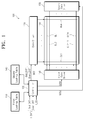
- FIG. 1 is a block diagram showing a display apparatus 101 according to an exemplary embodiment of the present disclosure and FIG. 2 is a graph showing first and second gamma curves respectively stored in first and second look-up tables shown in FIG. 1 .
- the display apparatus 101 includes a display panel 110, a controller 120, a first look-up table 130, a second look-up table 140, a first gate driver 150, a second gate driver 160, and a data driver 170.
- the display panel 110 includes a plurality of pixels PX each having one color of red, green, and blue colors.
- the display apparatus 101 is operated in an interlaced mode in which the pixels PX are grouped into two pixel groups, i.e., first and second pixel groups, and the first and second pixel groups are operated during different sub-frame periods.
- the controller 120 receives input image data I_DAT and an image control signal I_CS from an external image board (not shown).
- the input image data I_DAT may correspond to image data signals applied to the display apparatus 101 from the outside of the display apparatus 101.
- the input image data I_DAT provided from the image board include first input image data Odd_DAT corresponding to the first pixel group among the pixels PX and second input image data Even_DAT corresponding to the second pixel group among the pixels PX.
- the first pixel group includes the pixels positioned at odd-numbered pixel rows and the second pixel group includes the pixels positioned at even-numbered pixel rows.
- first and second pixel groups are alternately arranged with each other in the unit of one pixel row
- the first and second pixel groups may be alternately arranged with each other in the unit of two or more pixel rows, and in this case, the positions of the pixels included in each of the first and second pixel groups may be changed.
- a frame frequency of the display apparatus 101 becomes two times faster when an image is displayed through the display apparatus 101.
- the display apparatus 101 is operated at the frame frequency of about 120Hz to display the image.
- each of the pixels PX according to the present exemplary embodiment does not adopt a visible pixel structure.
- the term of "visible pixel structure” used herein means that one pixel includes two sub-pixels. In this case, one sub-pixel of the two sub-pixels receives high image data having a grayscale higher than that of an input grayscale and the other sub-pixel of the two sub-pixels receives low image data having a grayscale lower than that of the input grayscale.
- each of the pixels PX according to the present exemplary embodiment has what is herein referred to as an "invisible pixel structure" in which each pixel is not separated into two grayscale areas. With the invisible pixel structure, an aperture ratio of each pixel PX may be improved compared to that of the visible pixel structure.
- the display apparatus 101 may be operated in a time gamma mixed (TGM) driving method.
- TGM time gamma mixed
- one frame period is divided into at least two sub-frame periods, the high image data are applied to the pixels PX during one sub-frame period, and the low image data are applied to the pixels PX during the other sub-frame periods.
- the first look-up table 130 stores first sampling data sampled from a first gamma curve G1 shown in FIG. 2 and the second look-up table 140 stores second sampling data sampled from a second gamma curve G2 shown in FIG. 2 .
- an x-axis represents the grayscale and a y-axis represents a brightness (or transmittance (%)).
- the first gamma curve G1 has the brightness higher than that of the second gamma curve G2.
- FIG. 2 shows a reference gamma curve GR representing an optimized front visibility.
- the reference gamma curve GR has a gamma value of about 2.2.
- the first gamma curve G1 has a brightness higher than that of the reference gamma curve GR at the same grayscale and the second gamma curve G2 has the brightness lower than that of the reference gamma curve GR at the same grayscale.
- the first and second gamma curves G1 and G2 may be gamma curves optimized to the side visibility of the display panel 110.
- the first and second gamma curves G1 and G2 may be generated to calculate the reference gamma curve GR when the first and second gamma curves G1 and G2 are added to each other.
- the shape of the first and second gamma curves G1 and G2 should not be limited to FIG. 2 .
- the display panel 110 displays the image using data converted on the basis of the second gamma curve G2
- the display panel 110 displays the image with the brightness lower than that when the display panel 110 displays the image with data converted on the basis of the first gamma curve G1.
- the first look-up table 130 stores high grayscale brightness data extracted from the first gamma curve G1 among predetermined reference grayscales as the first sampling data.
- the second look-up table 140 stores low grayscale brightness data extracted from the second gamma curve G2 among the predetermined reference grayscales as the second sampling data.
- the controller 120 reads out the first and second sampling data from the first and second look-up tables 130 and 140 and converts the first and second input image data Odd_DAT and Even_DAT.
- Each of the first and second input image data Odd_DAT and Even_DAT include red, green, and blue image data R, G, and B.
- First and second converted image data Odd_DAT' and Even_DAT' generated by the controller 120 are provided to the data driver 170.
- the first and second converted image data Odd_DAT and Even DAT' may include information about gamma curve.
- the controller 120 generates a first gate control signal GCS1, a second gate control signal GCS2, and a data control signal DCS in response to the image control signal I_CS.
- the first gate driver 150 receives the first gate control signal GCS1 from the controller 120, generates odd-numbered gate signals in response to the first gate control signal GCS1, and applies the odd-numbered gate signals to the display panel 110.
- the second gate driver 160 receives the second gate control signal GCS2 from the controller 120, generates even-numbered gate signals in response to the second gate control signal GCS2, and applies the even-numbered gate signals to the display panel 110.
- the data driver 170 receives the first and second converted image data Odd_DAT' and Even_DAT' and the data control signal DCS from the controller 120 and applies data signal to the display panel 110 in response to the first and second converted image data Odd_DAT' and Even_DAT' and the data control signal DCS.
- the display panel 110 includes a plurality of gate lines GL1 to GL2n and a plurality of data lines DL1 to DLm.
- the gate lines GL1 to GL2n odd-numbered gate lines are connected to the first gate driver 150 to receive the odd-numbered gate signals and even-numbered gate lines are connected to the second gate driver 160 to receive the even-numbered gate signals.
- the data lines DL1 to DLm receive the data signals from the data driver 170.
- Each of the pixels PX included in the display panel 110 is connected to a corresponding gate line of the gate lines GL1 to GL2n and a corresponding data line of the data lines DL1 to DLm. Therefore, the pixels PX display the image in response to the gate signals and the data signals.
- FIG. 3 is a plan view showing an operation state of pixels during consecutive first and second frame periods Fn and Fn+1.
- the display apparatus 101 drives the pixels during consecutive first and second frame periods Fn and Fn+1 to display the image.
- the first frame period Fn includes first and second sub-frame periods Sub_F1 and Sub_F2 and the second frame period Fn+1 includes third and fourth sub-frame periods Sub_F3 and Sub_F4.
- the first pixel group displays a first grayscale image L1 using a first image signal generated on the basis of the first gamma curve G1 (refer to FIG. 2 ) during three sub-frame periods of the first to fourth sub-frame periods Sub_F1 to Sub_F4.
- the first pixel group displays a second grayscale image H1 using a second image signal generated on the basis of the second gamma curve G2 (refer to FIG. 2 ) during remaining one sub-frame period of the first to fourth sub-frame periods Sub_F1 to Sub_F4.
- the second pixel group displays a third grayscale image L2 using a third image signal generated on the basis of the first gamma curve G1 during three sub-frame periods of the first to fourth sub-frame periods Sub_F1 to Sub_F4.
- the second pixel group displays a fourth grayscale image H2 using a fourth image signal generated on the basis of the second gamma curve G2 during remaining one sub-frame period of the first to fourth sub-frame periods Sub_F1 to Sub_F4.
- the first pixel group includes the pixels positioned at odd-numbered pixel rows OR and the second pixel group includes the pixels positioned at even-numbered pixel rows ER.
- the first pixel group displays the first grayscale image L1 during the first to third sub-frame periods Sub_F1 to Sub_F3 and displays the second grayscale image H1 during the fourth sub-frame period Sub_F4.
- the second pixel group displays the third grayscale image L2 during the first, third, and fourth sub-frame periods Sub_F1, Sub_F3, and Sub_F4 and displays the fourth grayscale image H2 during the second sub-frame period Sub_F2.
- the sub-frame period i.e., the fourth sub-frame period Sub_F4, in which the first pixel group displays the second grayscale image H1
- the sub-frame i.e., the second sub-frame period Sub_F2, in which the second pixel group displays the fourth grayscale image H2.
- the odd-numbered pixel rows OR are sequentially turned on along a column direction during the first sub-frame period Sub_F1 to display the first grayscale image L1. Then, the odd-numbered pixel rows OR maintain the first grayscale image L1 during the second and third sub-frame periods Sub_F2 and Sub_F3.
- the even-numbered pixel rows ER are sequentially turned on along the column direction during the second sub-frame period Sub_F2 to display the fourth grayscale image H2. Then, the even-numbered pixel rows ER are sequentially turned on along the column direction during the third sub-frame period Sub_F3 to display the third grayscale image L2 and maintain the third grayscale image L2 during the fourth sub-frame period Sub_F4.
- Each of the first and second frame periods Fn and Fn+1 has a period width of about 1/60(ms) and each of the first to fourth sub-frame periods Sub_F1 to Sub_F4 has a period width of about 1/120 (ms).
- the odd-numbered pixel rows OR display the image in order of L1, L1, L1, and H1 (L1->L1->L1->H1) and the even-numbered pixel rows ER display the image in order of L2, H2, L2, and L2 (L2->H2->L2->L2).
- the display order of the images should not be limited thereto or thereby as long as the second and fourth grayscale images H1 and H2 having the high grayscale are displayed during one sub-frame period and the first and third grayscale images L1 and L2 having the low grayscale are displayed during three sub-frame periods.
- each pixel of the first pixel group displays the first grayscale image L1 and the second grayscale image H1 during the first to fourth sub-frame periods Sub_F1 to Sub_F4 to allow a time difference to exist between the first and second grayscale images L1 and H1. Accordingly, the side visibility is improved even though each pixel does not employ the visible pixel structure.
- each pixel of the second pixel group displays the third grayscale image L2 and the fourth grayscale image H2 during the first to fourth sub-frame periods Sub_F1 to Sub_F4 to allow a time difference to exist between the third and fourth grayscale images L2 and H2. Therefore, the side visibility of the display apparatus 101 may be improved without lowering the aperture ratio of each pixel PX of the display apparatus 101.
- FIGS. 4A to 4D are views showing a relation between an operation of the first and second gate drivers 150 and 160 shown in FIGS. 1 and 3 and the sub-frames and
- FIG. 5 is a waveform diagram showing first and second vertical start signals STV1 and STV2 and first to ninth gate signals shown in FIGS. 4A to 4D .
- the first gate driver 150 is operated during the first sub-frame period Sub_F1 and sequentially applies the odd-numbered gate signals (hereinafter, referred to as first, third, fifth, seventh, and ninth gate signals) to the odd-numbered gate lines GL1, GL3, GL5, GL7, and GL9 (hereinafter, referred to as first, third, fifth, seventh, and ninth gate lines) among the gate lines GL1 to GL2n.
- the second gate driver 160 is turned on during the first sub-frame period Sub_F1.
- the first gate driver 150 is connected to the first, third, fifth, seventh, and ninth gate lines GL1, GL3, GL5, GL7, and GL9 among the gate lines GL1 to GL2n and the second gate driver 160 is connected to the even-numbered gate lines GL2, GL4, GL6, and GL8 (hereinafter, referred to as second, fourth, sixth, and eighth gate lines) among the gate lines GL1 to GL2n.
- the first gate driver 150 receives the first vertical start signal STV1 from the controller 110 (refer to FIG. 1 ) and the second gate driver 160 receives the second vertical start signal STV2 from the controller 110.
- the first vertical start signal STV1 is one of signals included in the first gate control signal GCS1 and the second vertical start signal STV2 is one of signals included in the second gate control signal GCS2.
- the first vertical start signal STV1 is generated in a high state at a start time point of the first sub-frame period Sub_F1. Accordingly, when the first sub-frame period Sub_F1 starts, the first gate driver 150 starts its operation. The first gate driver 150 sequentially applies the first, third, fifth, seventh, and ninth gate signals to the first, third, fifth, seventh, and ninth gate lines GL1, GL3, GL5, GL7, and GL9 during the first sub-frame period Sub_F1.
- a high period, i.e., a horizontal scan period 1H, of each of the first, third, fifth, seventh, and ninth gate signals may be smaller than a value obtained by dividing the period width of the first sub-frame period Sub_F1 by the number of the odd-numbered gate lines, i.e., n number of the odd-numbered gate lines.
- the pixels of the odd-numbered pixel rows connected to the odd-numbered gate lines GL1, GL3, GL5, GL7, and GL9 receive a data signal corresponding to the first grayscale image L1 from the data driver 170.
- the second vertical start signal STV2 is maintained in a low state.
- the second gate driver 160 is maintained in the turned-off state. Accordingly, a new data signal is not applied to the pixels of the even-numbered pixel rows connected to the even-numbered gate lines GL2, GL4, GL6, and GL8, and thus the pixels of the even-numbered pixel rows maintain the data signal previously applied thereto.
- the second gate driver 160 is operated in response to the second vertical start signal STV2 and the first gate driver 150 is turned off.
- the second vertical start signal STV2 is generated in a high state at a start time point of the second sub-frame period Sub_F2. Accordingly, when the second sub-frame period Sub_F2 starts, the second gate driver 160 starts its operation.
- the second gate driver 160 sequentially applies the second, fourth, sixth, and eighth gate signals to the second, fourth, sixth, and eighth gate lines GL2, GL4, GL6, and GL8 during the second sub-frame period Sub_F2.
- a high period, i.e., the horizontal scan period 1H, of each of the second, fourth, sixth, and eighth gate signals may be smaller than a value obtained by dividing the period width of the second sub-frame period Sub_F2 by the number of the even-numbered gate lines, i.e., n number of the even-numbered gate lines.
- the pixels of the even-numbered pixel rows connected to the even-numbered gate lines GL2, GL4, GL6, and GL8 receive a data signal corresponding to the fourth grayscale image H2 from the data driver 170.
- the first vertical start signal STV1 is maintained in the low state.
- the first gate driver 150 is maintained in the turned-off state. Accordingly, a new data signal is not applied to the pixels of the odd-numbered pixel rows connected to the odd-numbered gate lines GL1, GL3, GL5, GL7, and GL9, and thus the pixels of the odd-numbered pixel rows maintain the data signal previously applied thereto.
- the second vertical start signal STV2 is generated in the high state at a start time point of the third sub-frame period Sub_F3. Accordingly, when the third sub-frame period Sub_F3 starts, the second gate driver 160 starts its operation.
- the second gate driver 160 sequentially applies the second, fourth, sixth, and eighth gate signals to the second, fourth, sixth, and eighth gate lines GL2, GL4, GL6, and GL8 during the third sub-frame period Sub_F3.
- the pixels of the even-numbered pixel rows connected to the even-numbered gate lines GL2, GL4, GL6, and GL8 receive a data signal corresponding to the third grayscale image L2 from the data driver 170.
- the first vertical start signal STV1 is maintained in the low state and the first gate driver 150 is maintained in the turned-off state. Accordingly, a new data signal is not applied to the pixels of the odd-numbered pixel rows connected to the odd-numbered gate lines GL1, GL3, GL5, GL7, and GL9, and thus the pixels of the odd-numbered pixel rows maintain the data signal previously applied thereto.
- the first vertical start signal STV1 is in the high state at the start of the fourth sub-frame period Sub_F4. Accordingly, the first gate driver 150 starts its operation when the fourth sub-frame period Sub_F4 starts.
- the first gate driver 150 sequentially applies the first, third, fifth, seventh, and ninth gate signals to the first, third, fifth, seventh, and ninth gate lines GL1, GL3, GL5, GL7, and GL9 during the fourth sub-frame period Sub_F4.
- the pixels of the odd-numbered pixel rows connected to the odd-numbered gate lines GL1, GL3, GL5, GL7, and GL9 receive a data signal corresponding to the second grayscale image H1 from the data driver 170.
- the second vertical start signal STV2 is maintained in the low state and the second gate driver 160 is maintained in the turned-off state. Accordingly, a new data signal is not applied to the pixels of the even-numbered pixel rows connected to the even-numbered gate lines GL2, GL4, GL6, and GL8, and thus the pixels of the even-numbered pixel rows maintain the data signal that was previously received.
- FIG. 6A is a view showing a movement of a quadrangular gray pattern on a display screen of a display panel
- FIG. 6B is a view showing a moving line-stain occurring in an LHLH interlaced scheme
- FIG. 6C is a view showing a moving line-stain removed in an LLLH interlaced scheme.
- a quadrangular gray pattern A1 is displayed on a white screen of the display panel 110.
- the quadrangular gray pattern A1 is assumed to move in a first direction D1 every one sub-frame period in the unit of two pixels.
- the display apparatus 101 displays the first grayscale image L1 through the odd-numbered pixel rows OR during the first sub-frame period Sub_F1 and displays the fourth grayscale image H2 through the even-numbered pixel rows ER during the second sub-frame period Sub_F2.
- the display apparatus 101 displays the second grayscale image H1 through the odd-numbered pixel rows OR during the third sub-frame period Sub_F3 and displays the third grayscale image L2 through the even-numbered pixel rows ER during the fourth sub-frame period Sub_F4.
- the quadrangular gray pattern A1 may be displayed as first, second, third, and fourth patterns P1, P2, P3, and P4, shown in graph in FIG. 6B and FIG. 6C .
- the first, second, third, and fourth patterns P1, P2, P3, and P4 are displayed during the first to fourth sub-frame periods Sub_F1 to Sub_F4, respectively, when the LLHH interlaced method is applied to the display apparatus 101.
- a left boundary of the first pattern P1 is displayed in a shape recessed in the first direction D1 in the first sub-frame period Sub_F1 and a boundary between a white area and a pattern area is not displayed in a straight line shape.
- a right boundary of the first pattern P1 is protruded in the first direction D1 without being displayed in the straight line shape.
- the second and fourth patterns P2 and P4 are displayed in the same quadrangular shape as the quadrangular gray pattern A1.
- the third pattern P3 in the third sub-frame period Sub_F3 is distorted similar to the shape of the first pattern P1 in the first sub-frame period Sub_F1. Accordingly, the quadrangular gray pattern A1 may be perceived as the distorted shape similar to the first and third patterns P1 and P3.
- the distortion in the shape of the patterns causes a brightness stain at the left and right boundaries, which is called the "moving line-stain.”
- the quadrangular gray pattern A1 is displayed in the shape shown in FIG. 6C during the first to fourth sub-frame periods Sub_F1 to Sub_F4.
- the pixels of the first pixel group are operated in an i-th sub-frame period Sub_F1 and an (i+3)th sub-frame period Sub_F4 among consecutive four sub-frame periods Sub_F1 to Sub_F4 to display the first and second grayscale images L1 and H1, respectively, and the pixels of the second pixel group are operated in an (i+1)th sub-frame period Sub_F2 and an (i+2)th sub-frame period Sub_F3 among the consecutive four sub-frame periods Sub_F1 to Sub_F4 to display the fourth and third grayscale images H2 and L2, respectively.
- the boundary between the white area and the pattern area is distorted without being displayed in the straight line shape at the left and right boundaries of the first and third patterns P1 and P3 of the first and third sub-frame periods Sub_F1 and Sub_F3.
- the distorted shape of the first pattern P1 in the first sub-frame period Sub_F1 is different from the distorted shape of the third pattern P3 in the third sub-frame period Sub_F3.
- the left boundary of the first pattern P1 in the first sub-frame period Sub_F1 is displayed in the shape recessed in the first direction D1
- the left boundary of the third pattern P3 of the third sub-frame period Sub_F3 is displayed in the shape protruded in a second direction D2 opposite the first direction D1.
- the right boundary of the first pattern P1 in the first sub-frame period Sub_F1 1 is displayed in the shape protruded in the first direction D1
- the right boundary of the third pattern P3 in the third sub-frame period Sub_F3 is displayed in the shape recessed in the second direction D2 opposite to the first direction D 1.
- the first pattern P1 in the first sub-frame period Sub_F1 and the third pattern P3 in the third sub-frame period Sub_F3 are added to each other, the brightness stain of the first pattern P1 is offset with the brightness stain of the third pattern P3 at the left and right boundaries. Therefore, the stain caused by the movement of the quadrangular gray pattern may be removed in the LLLH interlaced driving method.
- FIG. 7 is a block diagram showing a display apparatus 103 according to another exemplary embodiment of the present disclosure.
- the same reference numerals denote the same elements in FIG. 1 , and thus detailed descriptions of the same elements will be omitted.
- the display apparatus 103 includes a display panel 110, a controller 120, a gate driver 180, a switching part 190, and a data driver 170.
- the controller 120 generates a gate control signal GCS, a data control signal DCS, and a selection signal SL in response to the image control signal I_CS.
- the gate driver 180 receives the gate control signal GCS from the controller 120 and generates n gate signals in response to the gate control signal GCS.
- the switching part 190 receives the selection signal SL and selects a group of n odd-numbered gate lines or a group of n even-numbered gate lines among 2n gate lines GL1 to GL2n in response to the selection signal. Accordingly, the n gate signals output from the gate driver 180 may be applied to the n gate lines selected by the switching part 190.
- the data driver 170 receives first and second converted image data Odd_DAT' and Even_DAT' and the data control signal DCS and outputs data signals to the display panel 110 in response to the first and second converted image data Odd_DAT' and Even_DAT' and the data control signal DCS.
- the data driver 170 receives one of the first and second converted image data Odd_DAT' and Even_DAT' in synchronization with the operation with the switching part 190.
- FIGS. 8A to 8D are views showing a relation between sub-frames and the operation of the gate driver 180 and the switching part 190 shown in FIG. 7 and
- FIG. 9 is a waveform diagram showing a vertical start signal STV, a selection signal SL, and first to ninth gate signals shown in FIGS. 8A to 8D .
- the vertical start signal STV is generated in a high state at the start of each sub-frame period. Therefore, the gate driver 180 starts its operation every sub-frame period.
- Each of the first and second frame periods Fn and Fn+1 has a period width of about 1/60(ms) and each of the first to fourth sub-frame periods Sub_F1 to Sub_F4 has a period width of about 1/120 (ms).
- the gate driver 180 may be operated at a frequency of about 120Hz.
- the gate driver 180 is operated during the first sub-frame period Sub_F1 to sequentially output the n gate signals.
- the switching part 190 receives the selection signal.
- the switching part 190 includes first switching devices ST1 connected to the odd-numbered gate lines GL1, GL3, GL5, GL7, and GL9 among the gate lines GL1 to GL2n and second switching devices ST2 connected to the even-numbered gate lines GL2, GL4, GL6 and GL8 among the gate lines GL1 to GL2n.
- Each of the first switching devices ST1 is an N-type transistor and each of the second switching devices ST2 is a P-type transistor.
- the n gate signals sequentially output from the gate driver 190 are sequentially applied to the odd-numbered gate lines GL1, GL3, GL5, GL7, and GL9, i.e., first, third, fifth, seventh, and ninth gate lines, among the gate lines GL1 to GL2n.
- the pixels connected to the first, third, fifth, seventh, and ninth gate lines GL1, GL3, GL5, GL7, and GL9 are turned on and display a first grayscale image L1.
- the pixels connected to the even-numbered gate lines GL2, GL4, GL6, and GL8 maintain a previous grayscale image during the first sub-frame period Sub_F1.
- the selection signal SL is transitioned to a low state at the start of the second sub-frame period Sub_F2. Therefore, the first switching devices ST1 are turned off during the second sub-frame period Sub_F2 and the second switching devices ST2 are turned on during the second sub-frame period Sub_F2.
- the gate signals output from the gate driver 180 are sequentially applied to the second, fourth, sixth, and eighth gate lines GL2, GL4, GL6, and GL8 among the gate lines GL1 to GL2n through the second switching devices ST2 as the second, fourth, sixth, and eighth gate signals.
- the pixels arranged in the even-numbered pixel rows connected to the even-numbered gate lines GL2, GL4, GL6, and GL8 receive the data signal corresponding to the fourth grayscale image H2 from the data driver 170.
- the first switching devices ST1 are turned off during the second sub-frame period Sub_F2. Accordingly, a new data signal is not applied to the pixels of the odd-numbered pixel rows connected to the odd-numbered gate lines GL1, GL3, GL5, GL7, and GL9, and thus the pixels of the odd-numbered pixel rows maintain the data signal that was previously received.
- the selection signal SL is maintained in the low state during the third sub-frame period Sub_F3 and the gate driver 180 starts its operation when the third sub-frame period Sub_F3 starts. Therefore, the gate signals output from the gate driver 180 are sequentially applied to the second, fourth, sixth, and eighth gate lines GL2, GL4, GL6, and GL8 through the switching part 190.
- the pixels arranged in the even-numbered pixel rows connected to the even-numbered gate lines GL2, GL4, GL6, and GL8 receive the data signal corresponding to the third grayscale image L2 from the data driver 170.
- the first switching devices ST1 are turned off during the third sub-frame period Sub_F3. Accordingly, a new data signal is not applied to the pixels of the odd-numbered pixel rows connected to the odd-numbered gate lines GL1, GL3, GL5, GL7, and GL9, and thus the pixels of the odd-numbered pixel rows maintain the data signal previously applied thereto.
- the selection signal SL is transitioned to the high state at the start of the fourth sub-frame period Sub_F4. Therefore, the first switching devices ST1 are turned on and the second switching devices ST2 are turned off.
- the gate signals output from the gate driver 180 are sequentially applied to the first, third, fifth, seventh, and ninth gate lines GL1, GL3, GL5, GL7, and GL9 through the first switching devices ST1.
- the pixels arranged in the odd-numbered pixel rows connected to the odd-numbered gate lines GL1, GL3, GL5, GL7, and GL9 receive the data signal corresponding to the second grayscale image H1 from the data driver 170.
- the second switching devices ST2 are turned off during the fourth sub-frame period Sub_F4. Accordingly, a new data signal is not applied to the pixels of the even-numbered pixel rows connected to the even-numbered gate lines GL2, GL4, GL6, and GL8, and thus the pixels of the even-numbered pixel rows maintain the data signal that was previously received.
- FIG. 10 is a block diagram showing a display apparatus 105 according to another exemplary embodiment of the present disclosure.
- the same reference numerals denote the same elements in FIG. 1 , and thus detailed descriptions of the same elements will be omitted.
- the display apparatus 105 includes a display panel 110, a frame rate controller (hereinafter, referred to as FRC) 125, a controller 120, first and second gate drivers 150 and 160, and a data driver 170.
- FRC frame rate controller
- the display apparatus 105 has the same structure and function as those of the display apparatus 101 shown in FIG. 1 except that the display apparatus 105 further includes the FRC 125.
- the FRC 125 receives input image data I_DAT from the outside of the display apparatus 105, separates the input image data I_DAT into first and second input image data Odd_DAT and Even_DAT, and applies the first and second input image data Odd_DAT and Even_DAT to the controller 120. That is, the FRC 125 increases the frame frequency to time-divide an input frame period into two or more sub-frame periods. That is, the FRC 125 divides the image related to the pixel of each sub-frame period in accordance with each sub-frame period.
- the data processing process and the driving process by the controller 120, the first and second gate drivers 150 and 160, and the data driver 170 are substantially the same as those of the display apparatus 101 shown in FIG. 1 .
Abstract
Description
- The present disclosure relates to a display apparatus and a method of driving the same. More particularly, the present disclosure relates to a display apparatus capable of improving a display quality and a method of driving the display apparatus.
- In general, a liquid crystal display includes upper and lower substrates each being provided with a transparent electrode, liquid crystals injected between the upper and lower substrates, and upper and lower polarizers respectively disposed on outer surfaces of the upper and lower substrates. The liquid crystal display changes an alignment of the liquid crystals between the upper and lower substrates to control a transmittance of light passing through the liquid crystals.
- The liquid crystal display is operated in a horizontal electric field mode or in a vertical alignment mode. In the vertical alignment mode, the liquid crystals are aligned in a direction substantially vertical to the substrates and the liquid crystals rotate when voltages are applied to the upper and lower substrates. Accordingly, an optical axis of a liquid crystal layer moves and polarization of the light is controlled.
- The liquid crystal display operated in the vertical alignment mode adopts a structure wherein a pixel is divided into two sub-pixels in order to improve display quality and side visibility. When the pixel is divided into two or more sub-pixels, the number of signal lines and the number of thin film transistors increase since the two sub-pixels are individually driven. As a result, an aperture ratio of the liquid crystal display employing the pixel division structure decreases.
- The present disclosure provides a display apparatus capable of improving an aperture ratio and a display quality.
- The present disclosure provides a method of driving the display apparatus.
- Embodiments of the inventive concept provide a display apparatus including a plurality of pixels. A first pixel group of the pixels displays a first grayscale image on the basis of a first gamma curve during three sub-frame periods among consecutive first, second, third, and fourth sub-frame periods and displays a second grayscale image on the basis of a second gamma curve during a remaining one sub-frame period of the first, second, third, and fourth sub-frame periods. A second pixel group of the pixels displays a third grayscale image on the basis of the first gamma curve during three sub-frame periods among the first, second, third, and fourth sub-frame periods and displays a fourth grayscale image on the basis of the second gamma curve during a remaining one sub-frame period of the first, second, third, and fourth sub-frame periods.
- The sub-frame period in which the first pixel group displays the second grayscale image is different from the sub-frame period in which the second pixel group displays the fourth grayscale image.
- Embodiments of the inventive concept provide a driving method of a display apparatus including a plurality of pixels displaying an image during consecutive first, second, third, and fourth sub-frame periods. A first pixel group of the pixels displays a first grayscale image on the basis of a first gamma curve during three sub-frame periods among consecutive first, second, third, and fourth sub-frame periods and displays a second grayscale image on the basis of a second gamma curve during a remaining one sub-frame period of the first, second, third, and fourth sub-frame periods. A second pixel group of the pixels displays a third grayscale image on the basis of the first gamma curve during three sub-frame periods among the first, second, third, and fourth sub-frame periods and displays a fourth grayscale image on the basis of the second gamma curve during a remaining one sub-frame period of the first, second, third, and fourth sub-frame periods. The sub-frame period in which the first pixel group displays the second grayscale image is different from the sub-frame period in which the second pixel group displays the fourth grayscale image.
- According to the above, the side visibility of the display apparatus employing the invisible pixel structure may be improved without lowering the aperture ratio of the pixels.
- In addition, since the display apparatus is preferably operated in the LLLH interlaced method at a frequency of about 120Hz, a power consumption of the display apparatus is reduced and the moving line-stain is improved.
- The above and other advantages of the present disclosure will become readily apparent by reference to the following detailed description when considered in conjunction with the accompanying drawings wherein:
-
FIG. 1 is a block diagram showing a display apparatus according to an exemplary embodiment of the present disclosure; -
FIG. 2 is a graph showing first and second gamma curves respectively stored in first and second look-up tables shown inFIG. 1 ; -
FIG. 3 is a plan view showing an operation state of pixels during consecutive first and second frame periods; -
FIGS. 4A, 4B ,4C, and 4D are views showing a relation between an operation of first and second gate drivers shown inFIGS. 1 and3 and sub-frames; -
FIG. 5 is a waveform diagram showing first and second vertical start signals and first to ninth gate signals shown inFIGS. 4A to 4D ; -
FIG. 6A is a view showing a movement of a quadrangular gray pattern on a display screen of a display panel; -
FIG. 6B is a view showing a moving line-stain occurring in an LHLH interlaced scheme; -
FIG. 6C is a view showing a moving line-stain removed in an LLLH interlaced scheme; -
FIG. 7 is a block diagram showing a display apparatus according to another exemplary embodiment of the present disclosure; -
FIGS. 8A, 8B ,8C, and 8D are views showing a relation between sub-frames and an operation of a gate driver and a switching part shown inFIG. 7 ; -
FIG. 9 is a waveform diagram showing a vertical start signal, a selection signal, and first to ninth gate signals shown inFIGS. 8A to 8D ; and -
FIG. 10 is a block diagram showing a display apparatus according to another exemplary embodiment of the present disclosure. - It will be understood that when an element or layer is referred to as being "on", "connected to" or "coupled to" another element or layer, it can be directly on, connected or coupled to the other element or layer or intervening elements or layers may be present.
- It will be understood that, although the terms first, second, etc. may be used herein to describe various elements, components, regions, layers and/or sections, these elements, components, regions, layers and/or sections should not be limited by these terms. These terms are only used to distinguish one element, component, region, layer or section from another region, layer or section. Thus, a first element, component, region, layer or section discussed below could be termed a second element, component, region, layer or section without departing from the teachings of the present invention.
- The terminology used herein is for the purpose of describing particular embodiments only and is not intended to be limiting of the invention. As used herein, the singular forms, "a", "an" and "the" are intended to include the plural forms as well, unless the context clearly indicates otherwise. It will be further understood that the terms "includes" and/or "including", when used in this specification, specify the presence of stated features, integers, steps, operations, elements, and/or components, but do not preclude the presence or addition of one or more other features, integers, steps, operations, elements, components, and/or groups thereof.
- Unless otherwise defined, all terms (including technical and scientific terms) used herein have the same meaning as commonly understood by one of ordinary skill in the art to which this invention belongs. It will be further understood that terms, such as those defined in commonly used dictionaries, should be interpreted as having a meaning that is consistent with their meaning in the context of the relevant art and will not be interpreted in an idealized or overly formal sense unless expressly so defined herein.
- Hereinafter, the present inventive concept will be explained in detail with reference to the accompanying drawings.
-
FIG. 1 is a block diagram showing adisplay apparatus 101 according to an exemplary embodiment of the present disclosure andFIG. 2 is a graph showing first and second gamma curves respectively stored in first and second look-up tables shown inFIG. 1 . - Referring to
FIGS. 1 and2 , thedisplay apparatus 101 includes adisplay panel 110, acontroller 120, a first look-up table 130, a second look-up table 140, afirst gate driver 150, asecond gate driver 160, and adata driver 170. - The
display panel 110 includes a plurality of pixels PX each having one color of red, green, and blue colors. Thedisplay apparatus 101 is operated in an interlaced mode in which the pixels PX are grouped into two pixel groups, i.e., first and second pixel groups, and the first and second pixel groups are operated during different sub-frame periods. - The
controller 120 receives input image data I_DAT and an image control signal I_CS from an external image board (not shown). The input image data I_DAT may correspond to image data signals applied to thedisplay apparatus 101 from the outside of thedisplay apparatus 101. To allow thedisplay apparatus 101 to be operated in the interlaced mode, the input image data I_DAT provided from the image board include first input image data Odd_DAT corresponding to the first pixel group among the pixels PX and second input image data Even_DAT corresponding to the second pixel group among the pixels PX. As an example, the first pixel group includes the pixels positioned at odd-numbered pixel rows and the second pixel group includes the pixels positioned at even-numbered pixel rows. In the present exemplary embodiment, a structure that the first and second pixel groups are alternately arranged with each other in the unit of one pixel row will be described as a representative example, but they should not be limited thereto or thereby. That is, the first and second pixel groups may be alternately arranged with each other in the unit of two or more pixel rows, and in this case, the positions of the pixels included in each of the first and second pixel groups may be changed. - As described above, when the input image data I_DAT are separated into two image data Odd_DAT and Even_DAT and applied to the
controller 120, a frame frequency of thedisplay apparatus 101 becomes two times faster when an image is displayed through thedisplay apparatus 101. Thedisplay apparatus 101 is operated at the frame frequency of about 120Hz to display the image. - Each of the pixels PX according to the present exemplary embodiment does not adopt a visible pixel structure. Here, the term of "visible pixel structure" used herein means that one pixel includes two sub-pixels. In this case, one sub-pixel of the two sub-pixels receives high image data having a grayscale higher than that of an input grayscale and the other sub-pixel of the two sub-pixels receives low image data having a grayscale lower than that of the input grayscale. However, each of the pixels PX according to the present exemplary embodiment has what is herein referred to as an "invisible pixel structure" in which each pixel is not separated into two grayscale areas. With the invisible pixel structure, an aperture ratio of each pixel PX may be improved compared to that of the visible pixel structure.
- However, to improve the side visibility of the
display apparatus 101 employing the invisible pixel structure, thedisplay apparatus 101 may be operated in a time gamma mixed (TGM) driving method. According to the TGM driving method, one frame period is divided into at least two sub-frame periods, the high image data are applied to the pixels PX during one sub-frame period, and the low image data are applied to the pixels PX during the other sub-frame periods. - Hereinafter, a method of driving the
display apparatus 101 using the interlaced method and the TGM driving method will be described in detail. - The first look-up table 130 stores first sampling data sampled from a first gamma curve G1 shown in
FIG. 2 and the second look-up table 140 stores second sampling data sampled from a second gamma curve G2 shown inFIG. 2 . - In
FIG. 2 , an x-axis represents the grayscale and a y-axis represents a brightness (or transmittance (%)). As viewed relative to the same grayscale, the first gamma curve G1 has the brightness higher than that of the second gamma curve G2. -
FIG. 2 shows a reference gamma curve GR representing an optimized front visibility. For instance, the reference gamma curve GR has a gamma value of about 2.2. The first gamma curve G1 has a brightness higher than that of the reference gamma curve GR at the same grayscale and the second gamma curve G2 has the brightness lower than that of the reference gamma curve GR at the same grayscale. The first and second gamma curves G1 and G2 may be gamma curves optimized to the side visibility of thedisplay panel 110. The first and second gamma curves G1 and G2 may be generated to calculate the reference gamma curve GR when the first and second gamma curves G1 and G2 are added to each other. - The shape of the first and second gamma curves G1 and G2 should not be limited to
FIG. 2 . - Accordingly, when the
display panel 110 displays the image using data converted on the basis of the second gamma curve G2, thedisplay panel 110 displays the image with the brightness lower than that when thedisplay panel 110 displays the image with data converted on the basis of the first gamma curve G1. The first look-up table 130 stores high grayscale brightness data extracted from the first gamma curve G1 among predetermined reference grayscales as the first sampling data. The second look-up table 140 stores low grayscale brightness data extracted from the second gamma curve G2 among the predetermined reference grayscales as the second sampling data. - The
controller 120 reads out the first and second sampling data from the first and second look-up tables 130 and 140 and converts the first and second input image data Odd_DAT and Even_DAT. Each of the first and second input image data Odd_DAT and Even_DAT include red, green, and blue image data R, G, and B. First and second converted image data Odd_DAT' and Even_DAT' generated by thecontroller 120 are provided to thedata driver 170. The first and second converted image data Odd_DAT and Even DAT' may include information about gamma curve. - The
controller 120 generates a first gate control signal GCS1, a second gate control signal GCS2, and a data control signal DCS in response to the image control signal I_CS. Thefirst gate driver 150 receives the first gate control signal GCS1 from thecontroller 120, generates odd-numbered gate signals in response to the first gate control signal GCS1, and applies the odd-numbered gate signals to thedisplay panel 110. Thesecond gate driver 160 receives the second gate control signal GCS2 from thecontroller 120, generates even-numbered gate signals in response to the second gate control signal GCS2, and applies the even-numbered gate signals to thedisplay panel 110. Thedata driver 170 receives the first and second converted image data Odd_DAT' and Even_DAT' and the data control signal DCS from thecontroller 120 and applies data signal to thedisplay panel 110 in response to the first and second converted image data Odd_DAT' and Even_DAT' and the data control signal DCS. - The
display panel 110 includes a plurality of gate lines GL1 to GL2n and a plurality of data lines DL1 to DLm. Among the gate lines GL1 to GL2n, odd-numbered gate lines are connected to thefirst gate driver 150 to receive the odd-numbered gate signals and even-numbered gate lines are connected to thesecond gate driver 160 to receive the even-numbered gate signals. The data lines DL1 to DLm receive the data signals from thedata driver 170. Each of the pixels PX included in thedisplay panel 110 is connected to a corresponding gate line of the gate lines GL1 to GL2n and a corresponding data line of the data lines DL1 to DLm. Therefore, the pixels PX display the image in response to the gate signals and the data signals. -
FIG. 3 is a plan view showing an operation state of pixels during consecutive first and second frame periods Fn and Fn+1. - Referring to
FIG. 3 , thedisplay apparatus 101 drives the pixels during consecutive first and second frame periods Fn and Fn+1 to display the image. The first frame period Fn includes first and second sub-frame periods Sub_F1 and Sub_F2 and the second frame period Fn+1 includes third and fourth sub-frame periods Sub_F3 and Sub_F4. - Among the pixels PX, the first pixel group displays a first grayscale image L1 using a first image signal generated on the basis of the first gamma curve G1 (refer to
FIG. 2 ) during three sub-frame periods of the first to fourth sub-frame periods Sub_F1 to Sub_F4. The first pixel group displays a second grayscale image H1 using a second image signal generated on the basis of the second gamma curve G2 (refer toFIG. 2 ) during remaining one sub-frame period of the first to fourth sub-frame periods Sub_F1 to Sub_F4. - Among the pixels PX, the second pixel group displays a third grayscale image L2 using a third image signal generated on the basis of the first gamma curve G1 during three sub-frame periods of the first to fourth sub-frame periods Sub_F1 to Sub_F4. The second pixel group displays a fourth grayscale image H2 using a fourth image signal generated on the basis of the second gamma curve G2 during remaining one sub-frame period of the first to fourth sub-frame periods Sub_F1 to Sub_F4.
- Among the pixels PX, the first pixel group includes the pixels positioned at odd-numbered pixel rows OR and the second pixel group includes the pixels positioned at even-numbered pixel rows ER.
- As an example, the first pixel group displays the first grayscale image L1 during the first to third sub-frame periods Sub_F1 to Sub_F3 and displays the second grayscale image H1 during the fourth sub-frame period Sub_F4. The second pixel group displays the third grayscale image L2 during the first, third, and fourth sub-frame periods Sub_F1, Sub_F3, and Sub_F4 and displays the fourth grayscale image H2 during the second sub-frame period Sub_F2. As described above, the sub-frame period, i.e., the fourth sub-frame period Sub_F4, in which the first pixel group displays the second grayscale image H1, is different from the sub-frame, i.e., the second sub-frame period Sub_F2, in which the second pixel group displays the fourth grayscale image H2.
- The odd-numbered pixel rows OR are sequentially turned on along a column direction during the first sub-frame period Sub_F1 to display the first grayscale image L1. Then, the odd-numbered pixel rows OR maintain the first grayscale image L1 during the second and third sub-frame periods Sub_F2 and Sub_F3.
- The even-numbered pixel rows ER are sequentially turned on along the column direction during the second sub-frame period Sub_F2 to display the fourth grayscale image H2. Then, the even-numbered pixel rows ER are sequentially turned on along the column direction during the third sub-frame period Sub_F3 to display the third grayscale image L2 and maintain the third grayscale image L2 during the fourth sub-frame period Sub_F4.
- Each of the first and second frame periods Fn and Fn+1 has a period width of about 1/60(ms) and each of the first to fourth sub-frame periods Sub_F1 to Sub_F4 has a period width of about 1/120 (ms).
- Thus, during the consecutive first and second frame periods Fn and Fn+1, the odd-numbered pixel rows OR display the image in order of L1, L1, L1, and H1 (L1->L1->L1->H1) and the even-numbered pixel rows ER display the image in order of L2, H2, L2, and L2 (L2->H2->L2->L2). However, the display order of the images should not be limited thereto or thereby as long as the second and fourth grayscale images H1 and H2 having the high grayscale are displayed during one sub-frame period and the first and third grayscale images L1 and L2 having the low grayscale are displayed during three sub-frame periods.
- As described earlier, each pixel of the first pixel group displays the first grayscale image L1 and the second grayscale image H1 during the first to fourth sub-frame periods Sub_F1 to Sub_F4 to allow a time difference to exist between the first and second grayscale images L1 and H1. Accordingly, the side visibility is improved even though each pixel does not employ the visible pixel structure. In addition, each pixel of the second pixel group displays the third grayscale image L2 and the fourth grayscale image H2 during the first to fourth sub-frame periods Sub_F1 to Sub_F4 to allow a time difference to exist between the third and fourth grayscale images L2 and H2. Therefore, the side visibility of the
display apparatus 101 may be improved without lowering the aperture ratio of each pixel PX of thedisplay apparatus 101. -
FIGS. 4A to 4D are views showing a relation between an operation of the first andsecond gate drivers FIGS. 1 and3 and the sub-frames andFIG. 5 is a waveform diagram showing first and second vertical start signals STV1 and STV2 and first to ninth gate signals shown inFIGS. 4A to 4D . - Referring to
FIG. 4A , thefirst gate driver 150 is operated during the first sub-frame period Sub_F1 and sequentially applies the odd-numbered gate signals (hereinafter, referred to as first, third, fifth, seventh, and ninth gate signals) to the odd-numbered gate lines GL1, GL3, GL5, GL7, and GL9 (hereinafter, referred to as first, third, fifth, seventh, and ninth gate lines) among the gate lines GL1 to GL2n. Thesecond gate driver 160 is turned on during the first sub-frame period Sub_F1. - The
first gate driver 150 is connected to the first, third, fifth, seventh, and ninth gate lines GL1, GL3, GL5, GL7, and GL9 among the gate lines GL1 to GL2n and thesecond gate driver 160 is connected to the even-numbered gate lines GL2, GL4, GL6, and GL8 (hereinafter, referred to as second, fourth, sixth, and eighth gate lines) among the gate lines GL1 to GL2n. Thefirst gate driver 150 receives the first vertical start signal STV1 from the controller 110 (refer toFIG. 1 ) and thesecond gate driver 160 receives the second vertical start signal STV2 from thecontroller 110. The first vertical start signal STV1 is one of signals included in the first gate control signal GCS1 and the second vertical start signal STV2 is one of signals included in the second gate control signal GCS2. - As shown in
FIG. 5 , the first vertical start signal STV1 is generated in a high state at a start time point of the first sub-frame period Sub_F1. Accordingly, when the first sub-frame period Sub_F1 starts, thefirst gate driver 150 starts its operation. Thefirst gate driver 150 sequentially applies the first, third, fifth, seventh, and ninth gate signals to the first, third, fifth, seventh, and ninth gate lines GL1, GL3, GL5, GL7, and GL9 during the first sub-frame period Sub_F1. A high period, i.e., a horizontal scan period 1H, of each of the first, third, fifth, seventh, and ninth gate signals may be smaller than a value obtained by dividing the period width of the first sub-frame period Sub_F1 by the number of the odd-numbered gate lines, i.e., n number of the odd-numbered gate lines. - Therefore, the pixels of the odd-numbered pixel rows connected to the odd-numbered gate lines GL1, GL3, GL5, GL7, and GL9 receive a data signal corresponding to the first grayscale image L1 from the
data driver 170. - During the first sub-frame period Sub_F1, the second vertical start signal STV2 is maintained in a low state. Thus, the
second gate driver 160 is maintained in the turned-off state. Accordingly, a new data signal is not applied to the pixels of the even-numbered pixel rows connected to the even-numbered gate lines GL2, GL4, GL6, and GL8, and thus the pixels of the even-numbered pixel rows maintain the data signal previously applied thereto. - Referring to
FIGS. 4B and5 , thesecond gate driver 160 is operated in response to the second vertical start signal STV2 and thefirst gate driver 150 is turned off. - The second vertical start signal STV2 is generated in a high state at a start time point of the second sub-frame period Sub_F2. Accordingly, when the second sub-frame period Sub_F2 starts, the
second gate driver 160 starts its operation. Thesecond gate driver 160 sequentially applies the second, fourth, sixth, and eighth gate signals to the second, fourth, sixth, and eighth gate lines GL2, GL4, GL6, and GL8 during the second sub-frame period Sub_F2. A high period, i.e., the horizontal scan period 1H, of each of the second, fourth, sixth, and eighth gate signals may be smaller than a value obtained by dividing the period width of the second sub-frame period Sub_F2 by the number of the even-numbered gate lines, i.e., n number of the even-numbered gate lines. - Therefore, the pixels of the even-numbered pixel rows connected to the even-numbered gate lines GL2, GL4, GL6, and GL8 receive a data signal corresponding to the fourth grayscale image H2 from the
data driver 170. - During the second sub-frame period Sub_F2, the first vertical start signal STV1 is maintained in the low state. Thus, the
first gate driver 150 is maintained in the turned-off state. Accordingly, a new data signal is not applied to the pixels of the odd-numbered pixel rows connected to the odd-numbered gate lines GL1, GL3, GL5, GL7, and GL9, and thus the pixels of the odd-numbered pixel rows maintain the data signal previously applied thereto. - Referring to
FIGS. 4C and5 , the second vertical start signal STV2 is generated in the high state at a start time point of the third sub-frame period Sub_F3. Accordingly, when the third sub-frame period Sub_F3 starts, thesecond gate driver 160 starts its operation. Thesecond gate driver 160 sequentially applies the second, fourth, sixth, and eighth gate signals to the second, fourth, sixth, and eighth gate lines GL2, GL4, GL6, and GL8 during the third sub-frame period Sub_F3. - Therefore, the pixels of the even-numbered pixel rows connected to the even-numbered gate lines GL2, GL4, GL6, and GL8 receive a data signal corresponding to the third grayscale image L2 from the
data driver 170. - During the third sub-frame period Sub_F3, the first vertical start signal STV1 is maintained in the low state and the
first gate driver 150 is maintained in the turned-off state. Accordingly, a new data signal is not applied to the pixels of the odd-numbered pixel rows connected to the odd-numbered gate lines GL1, GL3, GL5, GL7, and GL9, and thus the pixels of the odd-numbered pixel rows maintain the data signal previously applied thereto. - Referring to
FIGS. 4D and5 , the first vertical start signal STV1 is in the high state at the start of the fourth sub-frame period Sub_F4. Accordingly, thefirst gate driver 150 starts its operation when the fourth sub-frame period Sub_F4 starts. Thefirst gate driver 150 sequentially applies the first, third, fifth, seventh, and ninth gate signals to the first, third, fifth, seventh, and ninth gate lines GL1, GL3, GL5, GL7, and GL9 during the fourth sub-frame period Sub_F4. - Therefore, the pixels of the odd-numbered pixel rows connected to the odd-numbered gate lines GL1, GL3, GL5, GL7, and GL9 receive a data signal corresponding to the second grayscale image H1 from the
data driver 170. - During the fourth sub-frame period Sub_F4, the second vertical start signal STV2 is maintained in the low state and the
second gate driver 160 is maintained in the turned-off state. Accordingly, a new data signal is not applied to the pixels of the even-numbered pixel rows connected to the even-numbered gate lines GL2, GL4, GL6, and GL8, and thus the pixels of the even-numbered pixel rows maintain the data signal that was previously received. -
FIG. 6A is a view showing a movement of a quadrangular gray pattern on a display screen of a display panel,FIG. 6B is a view showing a moving line-stain occurring in an LHLH interlaced scheme, andFIG. 6C is a view showing a moving line-stain removed in an LLLH interlaced scheme. - Referring to
FIGS. 6A and6B , a quadrangular gray pattern A1 is displayed on a white screen of thedisplay panel 110. The quadrangular gray pattern A1 is assumed to move in a first direction D1 every one sub-frame period in the unit of two pixels. - The
display apparatus 101 displays the first grayscale image L1 through the odd-numbered pixel rows OR during the first sub-frame period Sub_F1 and displays the fourth grayscale image H2 through the even-numbered pixel rows ER during the second sub-frame period Sub_F2. Thedisplay apparatus 101 displays the second grayscale image H1 through the odd-numbered pixel rows OR during the third sub-frame period Sub_F3 and displays the third grayscale image L2 through the even-numbered pixel rows ER during the fourth sub-frame period Sub_F4. - As described above, the quadrangular gray pattern A1 may be displayed as first, second, third, and fourth patterns P1, P2, P3, and P4, shown in graph in
FIG. 6B andFIG. 6C . The first, second, third, and fourth patterns P1, P2, P3, and P4 are displayed during the first to fourth sub-frame periods Sub_F1 to Sub_F4, respectively, when the LLHH interlaced method is applied to thedisplay apparatus 101. In particular, a left boundary of the first pattern P1 is displayed in a shape recessed in the first direction D1 in the first sub-frame period Sub_F1 and a boundary between a white area and a pattern area is not displayed in a straight line shape. A right boundary of the first pattern P1 is protruded in the first direction D1 without being displayed in the straight line shape. During the second and fourth sub-frame periods Sub_F2 and Sub_F4, the second and fourth patterns P2 and P4 are displayed in the same quadrangular shape as the quadrangular gray pattern A1. However, the third pattern P3 in the third sub-frame period Sub_F3 is distorted similar to the shape of the first pattern P1 in the first sub-frame period Sub_F1. Accordingly, the quadrangular gray pattern A1 may be perceived as the distorted shape similar to the first and third patterns P1 and P3. The distortion in the shape of the patterns causes a brightness stain at the left and right boundaries, which is called the "moving line-stain." - However, when the
display apparatus 101 is operated in the LLHH interlaced driving method shown inFIGS. 1 to 5 , the quadrangular gray pattern A1 is displayed in the shape shown inFIG. 6C during the first to fourth sub-frame periods Sub_F1 to Sub_F4. According to the LLHH interlaced driving method, the pixels of the first pixel group are operated in an i-th sub-frame period Sub_F1 and an (i+3)th sub-frame period Sub_F4 among consecutive four sub-frame periods Sub_F1 to Sub_F4 to display the first and second grayscale images L1 and H1, respectively, and the pixels of the second pixel group are operated in an (i+1)th sub-frame period Sub_F2 and an (i+2)th sub-frame period Sub_F3 among the consecutive four sub-frame periods Sub_F1 to Sub_F4 to display the fourth and third grayscale images H2 and L2, respectively. - Referring to
FIG. 6C , when the LLLH interlaced driving method is applied to thedisplay apparatus 101, the boundary between the white area and the pattern area is distorted without being displayed in the straight line shape at the left and right boundaries of the first and third patterns P1 and P3 of the first and third sub-frame periods Sub_F1 and Sub_F3. However, the distorted shape of the first pattern P1 in the first sub-frame period Sub_F1 is different from the distorted shape of the third pattern P3 in the third sub-frame period Sub_F3. In detail, when the left boundary of the first pattern P1 in the first sub-frame period Sub_F1 is displayed in the shape recessed in the first direction D1, the left boundary of the third pattern P3 of the third sub-frame period Sub_F3 is displayed in the shape protruded in a second direction D2 opposite the first direction D1. Similarly, when the right boundary of the first pattern P1 in the firstsub-frame period Sub_F1 1 is displayed in the shape protruded in the first direction D1, the right boundary of the third pattern P3 in the third sub-frame period Sub_F3 is displayed in the shape recessed in the second direction D2 opposite to thefirst direction D 1. - When the first pattern P1 in the first sub-frame period Sub_F1 and the third pattern P3 in the third sub-frame period Sub_F3 are added to each other, the brightness stain of the first pattern P1 is offset with the brightness stain of the third pattern P3 at the left and right boundaries. Therefore, the stain caused by the movement of the quadrangular gray pattern may be removed in the LLLH interlaced driving method.
-
FIG. 7 is a block diagram showing adisplay apparatus 103 according to another exemplary embodiment of the present disclosure. InFIG. 7 , the same reference numerals denote the same elements inFIG. 1 , and thus detailed descriptions of the same elements will be omitted. - Referring to
FIG. 7 , thedisplay apparatus 103 includes adisplay panel 110, acontroller 120, agate driver 180, a switchingpart 190, and adata driver 170. - The
controller 120 generates a gate control signal GCS, a data control signal DCS, and a selection signal SL in response to the image control signal I_CS. Thegate driver 180 receives the gate control signal GCS from thecontroller 120 and generates n gate signals in response to the gate control signal GCS. The switchingpart 190 receives the selection signal SL and selects a group of n odd-numbered gate lines or a group of n even-numbered gate lines among 2n gate lines GL1 to GL2n in response to the selection signal. Accordingly, the n gate signals output from thegate driver 180 may be applied to the n gate lines selected by the switchingpart 190. - The
data driver 170 receives first and second converted image data Odd_DAT' and Even_DAT' and the data control signal DCS and outputs data signals to thedisplay panel 110 in response to the first and second converted image data Odd_DAT' and Even_DAT' and the data control signal DCS. Thedata driver 170 receives one of the first and second converted image data Odd_DAT' and Even_DAT' in synchronization with the operation with the switchingpart 190. -
FIGS. 8A to 8D are views showing a relation between sub-frames and the operation of thegate driver 180 and the switchingpart 190 shown inFIG. 7 andFIG. 9 is a waveform diagram showing a vertical start signal STV, a selection signal SL, and first to ninth gate signals shown inFIGS. 8A to 8D . - Referring to
FIGS. 8A and9 , the vertical start signal STV is generated in a high state at the start of each sub-frame period. Therefore, thegate driver 180 starts its operation every sub-frame period. Each of the first and second frame periods Fn and Fn+1 has a period width of about 1/60(ms) and each of the first to fourth sub-frame periods Sub_F1 to Sub_F4 has a period width of about 1/120 (ms). When thegate driver 180 starts its operation every sub-frame period, thegate driver 180 may be operated at a frequency of about 120Hz. - The
gate driver 180 is operated during the first sub-frame period Sub_F1 to sequentially output the n gate signals. The switchingpart 190 receives the selection signal. As an example, the switchingpart 190 includes first switching devices ST1 connected to the odd-numbered gate lines GL1, GL3, GL5, GL7, and GL9 among the gate lines GL1 to GL2n and second switching devices ST2 connected to the even-numbered gate lines GL2, GL4, GL6 and GL8 among the gate lines GL1 to GL2n. Each of the first switching devices ST1 is an N-type transistor and each of the second switching devices ST2 is a P-type transistor. When the selection signal SL is in a high state, the first switching devices ST1 are turned on, but the second switching devices ST2 are turned off. Thus, the n gate signals sequentially output from thegate driver 190 are sequentially applied to the odd-numbered gate lines GL1, GL3, GL5, GL7, and GL9, i.e., first, third, fifth, seventh, and ninth gate lines, among the gate lines GL1 to GL2n. - Accordingly, the pixels connected to the first, third, fifth, seventh, and ninth gate lines GL1, GL3, GL5, GL7, and GL9 are turned on and display a first grayscale image L1. However, since the second switching devices ST2 are turned off, the pixels connected to the even-numbered gate lines GL2, GL4, GL6, and GL8 maintain a previous grayscale image during the first sub-frame period Sub_F1.
- Referring to
FIGS. 8B and9 , the selection signal SL is transitioned to a low state at the start of the second sub-frame period Sub_F2. Therefore, the first switching devices ST1 are turned off during the second sub-frame period Sub_F2 and the second switching devices ST2 are turned on during the second sub-frame period Sub_F2. The gate signals output from thegate driver 180 are sequentially applied to the second, fourth, sixth, and eighth gate lines GL2, GL4, GL6, and GL8 among the gate lines GL1 to GL2n through the second switching devices ST2 as the second, fourth, sixth, and eighth gate signals. - Thus, the pixels arranged in the even-numbered pixel rows connected to the even-numbered gate lines GL2, GL4, GL6, and GL8 receive the data signal corresponding to the fourth grayscale image H2 from the
data driver 170. - The first switching devices ST1 are turned off during the second sub-frame period Sub_F2. Accordingly, a new data signal is not applied to the pixels of the odd-numbered pixel rows connected to the odd-numbered gate lines GL1, GL3, GL5, GL7, and GL9, and thus the pixels of the odd-numbered pixel rows maintain the data signal that was previously received.
- Referring to
FIGS. 8C and9 , the selection signal SL is maintained in the low state during the third sub-frame period Sub_F3 and thegate driver 180 starts its operation when the third sub-frame period Sub_F3 starts. Therefore, the gate signals output from thegate driver 180 are sequentially applied to the second, fourth, sixth, and eighth gate lines GL2, GL4, GL6, and GL8 through the switchingpart 190. - Thus, the pixels arranged in the even-numbered pixel rows connected to the even-numbered gate lines GL2, GL4, GL6, and GL8 receive the data signal corresponding to the third grayscale image L2 from the
data driver 170. - The first switching devices ST1 are turned off during the third sub-frame period Sub_F3. Accordingly, a new data signal is not applied to the pixels of the odd-numbered pixel rows connected to the odd-numbered gate lines GL1, GL3, GL5, GL7, and GL9, and thus the pixels of the odd-numbered pixel rows maintain the data signal previously applied thereto.
- Referring to
FIGS. 8D and9 , the selection signal SL is transitioned to the high state at the start of the fourth sub-frame period Sub_F4. Therefore, the first switching devices ST1 are turned on and the second switching devices ST2 are turned off. The gate signals output from thegate driver 180 are sequentially applied to the first, third, fifth, seventh, and ninth gate lines GL1, GL3, GL5, GL7, and GL9 through the first switching devices ST1. - Thus, the pixels arranged in the odd-numbered pixel rows connected to the odd-numbered gate lines GL1, GL3, GL5, GL7, and GL9 receive the data signal corresponding to the second grayscale image H1 from the
data driver 170. - The second switching devices ST2 are turned off during the fourth sub-frame period Sub_F4. Accordingly, a new data signal is not applied to the pixels of the even-numbered pixel rows connected to the even-numbered gate lines GL2, GL4, GL6, and GL8, and thus the pixels of the even-numbered pixel rows maintain the data signal that was previously received.
-
FIG. 10 is a block diagram showing adisplay apparatus 105 according to another exemplary embodiment of the present disclosure. InFIG. 10 , the same reference numerals denote the same elements inFIG. 1 , and thus detailed descriptions of the same elements will be omitted. - Referring to
FIG. 10 , thedisplay apparatus 105 includes adisplay panel 110, a frame rate controller (hereinafter, referred to as FRC) 125, acontroller 120, first andsecond gate drivers data driver 170. - The
display apparatus 105 has the same structure and function as those of thedisplay apparatus 101 shown inFIG. 1 except that thedisplay apparatus 105 further includes theFRC 125. TheFRC 125 receives input image data I_DAT from the outside of thedisplay apparatus 105, separates the input image data I_DAT into first and second input image data Odd_DAT and Even_DAT, and applies the first and second input image data Odd_DAT and Even_DAT to thecontroller 120. That is, theFRC 125 increases the frame frequency to time-divide an input frame period into two or more sub-frame periods. That is, theFRC 125 divides the image related to the pixel of each sub-frame period in accordance with each sub-frame period. - The data processing process and the driving process by the
controller 120, the first andsecond gate drivers data driver 170 are substantially the same as those of thedisplay apparatus 101 shown inFIG. 1 . - Although the exemplary embodiments of the present invention have been described, it is understood that the present invention should not be limited to these exemplary embodiments but various changes and modifications can be made by one ordinary skilled in the art within the scope of the present invention as hereinafter claimed.
Claims (10)
- A display apparatus (101, 103, 105) comprising:a plurality of pixels (PX), a first pixel group of the pixels (PX) configured to display a first grayscale image (L1) based on a first gamma curve (G1) during three sub-frame periods among consecutive first, second, third, and fourth sub-frame periods (Sub_F1..Sub_F4) and configured to display a second grayscale image (H1) based on a second gamma curve (G2) during a remaining one sub-frame period of the first, second, third, and fourth sub-frame periods (Sub_F1..Sub_F4), a second pixel group of the pixels (PX) configured to display a third grayscale image (L2) based on the first gamma curve (G1) during three sub-frame periods among the first, second, third, and fourth sub-frame periods (Sub_F1..Sub_F4) and configured to display a fourth grayscale image (H2) based on the second gamma curve (G2) during a remaining one sub-frame period of the first, second, third, and fourth sub-frame periods (Sub_F1..Sub_F4),wherein the sub-frame period in which the first pixel group displays the second grayscale image (H1) is different from the sub-frame period in which the second pixel group displays the fourth grayscale image (H2).
- The display apparatus (101, 103, 105) of claim 1, wherein the pixels (PX) are arranged in a matrix form,
the display apparatus (101, 103, 105) further comprises a plurality of gate lines (GL1-GL2n) arranged in a row direction and sequentially scanned in the row direction, and
the first and second pixel groups are alternately arranged with each other in the row direction. - The display apparatus (101, 103, 105) of claim 2, wherein the first pixel group comprises odd-numbered pixel rows (OR) among the pixels (PX), the odd-numbered pixel rows (OR) are sequentially turned on in a column direction to display the first grayscale image (L1) during the first sub-frame period, the second pixel group comprises even-numbered pixel rows (ER) among the pixels (PX), and the even-numbered pixel rows (ER) are sequentially turned on in the column direction to display the third grayscale image (L2) during the third sub-frame period.
- The display apparatus (101, 103, 105) of one of claims 1 to 3, wherein the first pixel group maintains the first grayscale image (L1) during the second and third sub-frame periods.
- The display apparatus (101, 103, 105) of claim 3 or of claims 3 and 4, wherein the even-numbered pixel rows (ER) are sequentially turned on in the column direction to display the fourth grayscale image (H2) during the second sub-frame period.
- The display apparatus (101, 103, 105) of claim 5, wherein the odd-numbered pixel rows (OR) are sequentially turned on in the column direction to display the second grayscale image (H1) during the fourth sub-frame period.
- The display apparatus (101, 103, 105) of one of claims 3 to 6, further comprising:a first gate driver (150) connected to odd-numbered gate lines among the gate lines (GL1-GL2n) to sequentially drive the odd-numbered pixel rows (OR); anda second gate driver (160) connected to even-numbered gate lines among the gate lines (GL1-GL2n) to sequentially drive the even-numbered pixel rows (ER).
- The display apparatus (101, 103, 105) of claim 7, wherein the first and second gate drivers (150, 160) are alternately operated with each other, the first gate driver (150) is operated during the first and fourth sub-frame periods, and the second gate driver (160) is operated during the second and third sub-frame periods.
- The display apparatus (101, 103, 105) of one of claims 7 or 8, wherein the first gate driver (150) receives a first vertical start signal (STV1) generated in a high state at a start of the first sub-frame period and a start of the fourth sub-frame period, and the second gate driver (160) receives a second vertical start signal (STV2) generated in a high state at a start of the second sub-frame period and a start of the third sub-frame period.
- The display apparatus (101, 103, 105) of one of claims 1 to 9, wherein the first and second gamma curves (G1, G2) have different brightness values from each other at a same grayscale level.
Applications Claiming Priority (1)
| Application Number | Priority Date | Filing Date | Title |
|---|---|---|---|
| KR1020150018107A KR102335779B1 (en) | 2015-02-05 | 2015-02-05 | Display apparatus and method of driving the same |
Publications (2)
| Publication Number | Publication Date |
|---|---|
| EP3054441A1 true EP3054441A1 (en) | 2016-08-10 |
| EP3054441B1 EP3054441B1 (en) | 2019-06-19 |
Family
ID=55272303
Family Applications (1)
| Application Number | Title | Priority Date | Filing Date |
|---|---|---|---|
| EP16153279.1A Active EP3054441B1 (en) | 2015-02-05 | 2016-01-29 | Display apparatus |
Country Status (4)
| Country | Link |
|---|---|
| US (1) | US9865203B2 (en) |
| EP (1) | EP3054441B1 (en) |
| KR (1) | KR102335779B1 (en) |
| CN (1) | CN105869585B (en) |
Cited By (2)
| Publication number | Priority date | Publication date | Assignee | Title |
|---|---|---|---|---|
| EP3648622B1 (en) | 2017-07-07 | 2021-08-04 | International Tobacco Machinery Poland Sp. z o.o. | A machine for producing multi-segment rods and a method for cleaning a machine for producing multi-segment rods |
| CN113593491A (en) * | 2021-07-13 | 2021-11-02 | Tcl华星光电技术有限公司 | Display panel driving method, display panel and display device |
Families Citing this family (3)
| Publication number | Priority date | Publication date | Assignee | Title |
|---|---|---|---|---|
| KR102364433B1 (en) * | 2015-07-13 | 2022-02-18 | 삼성디스플레이 주식회사 | Display device and driving method thereof |
| KR102330027B1 (en) * | 2018-03-20 | 2021-11-23 | 삼성전자 주식회사 | Elelectronic device and method for driving display thereof |
| KR102510841B1 (en) * | 2018-04-04 | 2023-03-17 | 삼성전자주식회사 | A method for driving a plurality of pixel lines and an electronic device thereof |
Citations (3)
| Publication number | Priority date | Publication date | Assignee | Title |
|---|---|---|---|---|
| EP1959420A2 (en) * | 2007-02-14 | 2008-08-20 | Samsung Electronics Co., Ltd. | Driving apparatus of display device and display device including the same |
| EP2669882A2 (en) * | 2012-05-31 | 2013-12-04 | Samsung Display Co., Ltd. | Display device and driving method thereof |
| US20140002509A1 (en) * | 2012-06-29 | 2014-01-02 | Samsung Display Co., Ltd. | Method of driving display device |
Family Cites Families (16)
| Publication number | Priority date | Publication date | Assignee | Title |
|---|---|---|---|---|
| TWI251199B (en) | 2003-03-31 | 2006-03-11 | Sharp Kk | Image processing method and liquid-crystal display device using the same |
| KR20060111262A (en) | 2005-04-22 | 2006-10-26 | 삼성전자주식회사 | Driving apparatus of display device |
| KR101222983B1 (en) | 2006-11-06 | 2013-01-17 | 엘지디스플레이 주식회사 | LCD and drive method thereof |
| KR101471154B1 (en) | 2008-06-17 | 2014-12-09 | 삼성디스플레이 주식회사 | Method for driving pixel and display apparatus for performing the method |
| KR101521519B1 (en) | 2008-07-11 | 2015-05-20 | 삼성디스플레이 주식회사 | Methode for driving a display panel and display apparatus for performing the method |
| KR101322002B1 (en) | 2008-11-27 | 2013-10-25 | 엘지디스플레이 주식회사 | Liquid Crystal Display |
| JP2011007889A (en) | 2009-06-24 | 2011-01-13 | Videocon Global Ltd | Liquid crystal display device |
| US20120194572A1 (en) * | 2009-08-27 | 2012-08-02 | Sharp Kabushiki Kaisha | Display device |
| EP2549324A4 (en) * | 2010-03-19 | 2013-09-04 | Sharp Kk | Liquid crystal display device |
| KR20120025187A (en) | 2010-09-07 | 2012-03-15 | 삼성전자주식회사 | Method of driving liquid crystal display panel and liquid crystal display device performing the method |
| KR101987799B1 (en) * | 2012-05-31 | 2019-06-12 | 삼성디스플레이 주식회사 | Display device and driving method thereof |
| KR101991897B1 (en) * | 2012-06-29 | 2019-06-24 | 삼성디스플레이 주식회사 | Display device and driving method thereof |
| KR101539028B1 (en) | 2012-07-05 | 2015-07-24 | 성균관대학교산학협력단 | Field sequential display method liquid crystal display apparatus |
| KR101441395B1 (en) * | 2012-07-05 | 2014-09-17 | 엘지디스플레이 주식회사 | Liquid crystal display device and driving method the same |
| KR20140033951A (en) | 2012-09-11 | 2014-03-19 | 성균관대학교산학협력단 | Field sequential display method liquid crystal display apparatus |
| KR102070657B1 (en) * | 2012-12-03 | 2020-01-30 | 삼성디스플레이 주식회사 | Display apparatus and method of driving the same |
-
2015
- 2015-02-05 KR KR1020150018107A patent/KR102335779B1/en active IP Right Grant
-
2016
- 2016-01-29 EP EP16153279.1A patent/EP3054441B1/en active Active
- 2016-02-04 US US15/016,111 patent/US9865203B2/en active Active
- 2016-02-04 CN CN201610079637.3A patent/CN105869585B/en active Active
Patent Citations (3)
| Publication number | Priority date | Publication date | Assignee | Title |
|---|---|---|---|---|
| EP1959420A2 (en) * | 2007-02-14 | 2008-08-20 | Samsung Electronics Co., Ltd. | Driving apparatus of display device and display device including the same |
| EP2669882A2 (en) * | 2012-05-31 | 2013-12-04 | Samsung Display Co., Ltd. | Display device and driving method thereof |
| US20140002509A1 (en) * | 2012-06-29 | 2014-01-02 | Samsung Display Co., Ltd. | Method of driving display device |
Cited By (3)
| Publication number | Priority date | Publication date | Assignee | Title |
|---|---|---|---|---|
| EP3648622B1 (en) | 2017-07-07 | 2021-08-04 | International Tobacco Machinery Poland Sp. z o.o. | A machine for producing multi-segment rods and a method for cleaning a machine for producing multi-segment rods |
| CN113593491A (en) * | 2021-07-13 | 2021-11-02 | Tcl华星光电技术有限公司 | Display panel driving method, display panel and display device |
| CN113593491B (en) * | 2021-07-13 | 2022-08-05 | Tcl华星光电技术有限公司 | Display panel driving method, display panel and display device |
Also Published As
| Publication number | Publication date |
|---|---|
| KR20160096776A (en) | 2016-08-17 |
| US9865203B2 (en) | 2018-01-09 |
| EP3054441B1 (en) | 2019-06-19 |
| CN105869585A (en) | 2016-08-17 |
| CN105869585B (en) | 2020-09-01 |
| US20160232860A1 (en) | 2016-08-11 |
| KR102335779B1 (en) | 2021-12-08 |
Similar Documents
| Publication | Publication Date | Title |
|---|---|---|
| KR102306598B1 (en) | Display apparatus | |
| KR101112554B1 (en) | Driving apparatus for display device and display device including the same | |
| EP2525349B1 (en) | Gate driver and liquid crystal display including the same | |
| KR101341906B1 (en) | Driving circuit for liquid crystal display device and method for driving the same | |
| US20140125647A1 (en) | Liquid crystal display device and method of driving the same | |
| EP3054441B1 (en) | Display apparatus | |
| US9852698B2 (en) | Display apparatus and driving method thereof using a time/space division scheme | |
| US10140937B2 (en) | Display panel, liquid crystal display and driving method therefor | |
| KR102020354B1 (en) | Display apparatus | |
| US9978322B2 (en) | Display apparatus | |
| US20140168281A1 (en) | Method of driving display panel and liquid crystal display apparatus for performing the same | |
| US11302272B2 (en) | Display device, and driving method for the display device for reducing power consumption and improving display effect | |
| US8963912B2 (en) | Display device and display device driving method | |
| US11017709B2 (en) | Driving method for pixel matrix and display device | |
| US9734778B2 (en) | Display apparatus having increased lateral image quality | |
| KR101307950B1 (en) | Liquid crystal display and driving method thereof | |
| TWI408648B (en) | Field sequential lcd driving method | |
| KR20160044672A (en) | Method of driving display panel, display panel driving apparatus and display apparatus having the display panel driving apparatus | |
| KR101343498B1 (en) | Liquid crystal display device | |
| KR102279815B1 (en) | Liquid crystal display device and driving method thereof | |
| KR20130020308A (en) | Method of driving liquid crystal panel | |
| CN109584830A (en) | The driving device of display and its display panel, method | |
| KR101119906B1 (en) | Apparatus for image display | |
| KR20050001062A (en) | Liquid Crystal Display And Driving Method Thereof | |
| KR101192800B1 (en) | A liquid crystal display device and a method for diving the same |
Legal Events
| Date | Code | Title | Description |
|---|---|---|---|
| PUAI | Public reference made under article 153(3) epc to a published international application that has entered the european phase |
Free format text: ORIGINAL CODE: 0009012 |
|
| AK | Designated contracting states |
Kind code of ref document: A1 Designated state(s): AL AT BE BG CH CY CZ DE DK EE ES FI FR GB GR HR HU IE IS IT LI LT LU LV MC MK MT NL NO PL PT RO RS SE SI SK SM TR |
|
| AX | Request for extension of the european patent |
Extension state: BA ME |
|
| STAA | Information on the status of an ep patent application or granted ep patent |
Free format text: STATUS: REQUEST FOR EXAMINATION WAS MADE |
|
| 17P | Request for examination filed |
Effective date: 20170203 |
|
| RBV | Designated contracting states (corrected) |
Designated state(s): AL AT BE BG CH CY CZ DE DK EE ES FI FR GB GR HR HU IE IS IT LI LT LU LV MC MK MT NL NO PL PT RO RS SE SI SK SM TR |
|
| STAA | Information on the status of an ep patent application or granted ep patent |
Free format text: STATUS: EXAMINATION IS IN PROGRESS |
|
| 17Q | First examination report despatched |
Effective date: 20170502 |
|
| GRAP | Despatch of communication of intention to grant a patent |
Free format text: ORIGINAL CODE: EPIDOSNIGR1 |
|
| STAA | Information on the status of an ep patent application or granted ep patent |
Free format text: STATUS: GRANT OF PATENT IS INTENDED |
|
| RAP1 | Party data changed (applicant data changed or rights of an application transferred) |
Owner name: SAMSUNG DISPLAY CO., LTD. |
|
| INTG | Intention to grant announced |
Effective date: 20190111 |
|
| GRAS | Grant fee paid |
Free format text: ORIGINAL CODE: EPIDOSNIGR3 |
|
| GRAA | (expected) grant |
Free format text: ORIGINAL CODE: 0009210 |
|
| STAA | Information on the status of an ep patent application or granted ep patent |
Free format text: STATUS: THE PATENT HAS BEEN GRANTED |
|
| AK | Designated contracting states |
Kind code of ref document: B1 Designated state(s): AL AT BE BG CH CY CZ DE DK EE ES FI FR GB GR HR HU IE IS IT LI LT LU LV MC MK MT NL NO PL PT RO RS SE SI SK SM TR |
|
| REG | Reference to a national code |
Ref country code: GB Ref legal event code: FG4D |
|
| REG | Reference to a national code |
Ref country code: CH Ref legal event code: EP |
|
| REG | Reference to a national code |
Ref country code: NL Ref legal event code: FP Ref country code: IE Ref legal event code: FG4D |
|
| REG | Reference to a national code |
Ref country code: DE Ref legal event code: R096 Ref document number: 602016015366 Country of ref document: DE |
|
| REG | Reference to a national code |
Ref country code: AT Ref legal event code: REF Ref document number: 1146497 Country of ref document: AT Kind code of ref document: T Effective date: 20190715 |
|
| PG25 | Lapsed in a contracting state [announced via postgrant information from national office to epo] |
Ref country code: LT Free format text: LAPSE BECAUSE OF FAILURE TO SUBMIT A TRANSLATION OF THE DESCRIPTION OR TO PAY THE FEE WITHIN THE PRESCRIBED TIME-LIMIT Effective date: 20190619 Ref country code: HR Free format text: LAPSE BECAUSE OF FAILURE TO SUBMIT A TRANSLATION OF THE DESCRIPTION OR TO PAY THE FEE WITHIN THE PRESCRIBED TIME-LIMIT Effective date: 20190619 Ref country code: FI Free format text: LAPSE BECAUSE OF FAILURE TO SUBMIT A TRANSLATION OF THE DESCRIPTION OR TO PAY THE FEE WITHIN THE PRESCRIBED TIME-LIMIT Effective date: 20190619 Ref country code: AL Free format text: LAPSE BECAUSE OF FAILURE TO SUBMIT A TRANSLATION OF THE DESCRIPTION OR TO PAY THE FEE WITHIN THE PRESCRIBED TIME-LIMIT Effective date: 20190619 Ref country code: NO Free format text: LAPSE BECAUSE OF FAILURE TO SUBMIT A TRANSLATION OF THE DESCRIPTION OR TO PAY THE FEE WITHIN THE PRESCRIBED TIME-LIMIT Effective date: 20190919 Ref country code: SE Free format text: LAPSE BECAUSE OF FAILURE TO SUBMIT A TRANSLATION OF THE DESCRIPTION OR TO PAY THE FEE WITHIN THE PRESCRIBED TIME-LIMIT Effective date: 20190619 |
|
| REG | Reference to a national code |
Ref country code: LT Ref legal event code: MG4D |
|
| PG25 | Lapsed in a contracting state [announced via postgrant information from national office to epo] |
Ref country code: BG Free format text: LAPSE BECAUSE OF FAILURE TO SUBMIT A TRANSLATION OF THE DESCRIPTION OR TO PAY THE FEE WITHIN THE PRESCRIBED TIME-LIMIT Effective date: 20190919 Ref country code: LV Free format text: LAPSE BECAUSE OF FAILURE TO SUBMIT A TRANSLATION OF THE DESCRIPTION OR TO PAY THE FEE WITHIN THE PRESCRIBED TIME-LIMIT Effective date: 20190619 Ref country code: GR Free format text: LAPSE BECAUSE OF FAILURE TO SUBMIT A TRANSLATION OF THE DESCRIPTION OR TO PAY THE FEE WITHIN THE PRESCRIBED TIME-LIMIT Effective date: 20190920 Ref country code: RS Free format text: LAPSE BECAUSE OF FAILURE TO SUBMIT A TRANSLATION OF THE DESCRIPTION OR TO PAY THE FEE WITHIN THE PRESCRIBED TIME-LIMIT Effective date: 20190619 |
|
| REG | Reference to a national code |
Ref country code: AT Ref legal event code: MK05 Ref document number: 1146497 Country of ref document: AT Kind code of ref document: T Effective date: 20190619 |
|
| PG25 | Lapsed in a contracting state [announced via postgrant information from national office to epo] |
Ref country code: EE Free format text: LAPSE BECAUSE OF FAILURE TO SUBMIT A TRANSLATION OF THE DESCRIPTION OR TO PAY THE FEE WITHIN THE PRESCRIBED TIME-LIMIT Effective date: 20190619 Ref country code: PT Free format text: LAPSE BECAUSE OF FAILURE TO SUBMIT A TRANSLATION OF THE DESCRIPTION OR TO PAY THE FEE WITHIN THE PRESCRIBED TIME-LIMIT Effective date: 20191021 Ref country code: SK Free format text: LAPSE BECAUSE OF FAILURE TO SUBMIT A TRANSLATION OF THE DESCRIPTION OR TO PAY THE FEE WITHIN THE PRESCRIBED TIME-LIMIT Effective date: 20190619 Ref country code: RO Free format text: LAPSE BECAUSE OF FAILURE TO SUBMIT A TRANSLATION OF THE DESCRIPTION OR TO PAY THE FEE WITHIN THE PRESCRIBED TIME-LIMIT Effective date: 20190619 Ref country code: CZ Free format text: LAPSE BECAUSE OF FAILURE TO SUBMIT A TRANSLATION OF THE DESCRIPTION OR TO PAY THE FEE WITHIN THE PRESCRIBED TIME-LIMIT Effective date: 20190619 Ref country code: AT Free format text: LAPSE BECAUSE OF FAILURE TO SUBMIT A TRANSLATION OF THE DESCRIPTION OR TO PAY THE FEE WITHIN THE PRESCRIBED TIME-LIMIT Effective date: 20190619 |
|
| PG25 | Lapsed in a contracting state [announced via postgrant information from national office to epo] |
Ref country code: SM Free format text: LAPSE BECAUSE OF FAILURE TO SUBMIT A TRANSLATION OF THE DESCRIPTION OR TO PAY THE FEE WITHIN THE PRESCRIBED TIME-LIMIT Effective date: 20190619 Ref country code: IS Free format text: LAPSE BECAUSE OF FAILURE TO SUBMIT A TRANSLATION OF THE DESCRIPTION OR TO PAY THE FEE WITHIN THE PRESCRIBED TIME-LIMIT Effective date: 20191019 Ref country code: IT Free format text: LAPSE BECAUSE OF FAILURE TO SUBMIT A TRANSLATION OF THE DESCRIPTION OR TO PAY THE FEE WITHIN THE PRESCRIBED TIME-LIMIT Effective date: 20190619 Ref country code: ES Free format text: LAPSE BECAUSE OF FAILURE TO SUBMIT A TRANSLATION OF THE DESCRIPTION OR TO PAY THE FEE WITHIN THE PRESCRIBED TIME-LIMIT Effective date: 20190619 |
|
| PG25 | Lapsed in a contracting state [announced via postgrant information from national office to epo] |
Ref country code: TR Free format text: LAPSE BECAUSE OF FAILURE TO SUBMIT A TRANSLATION OF THE DESCRIPTION OR TO PAY THE FEE WITHIN THE PRESCRIBED TIME-LIMIT Effective date: 20190619 |
|
| PG25 | Lapsed in a contracting state [announced via postgrant information from national office to epo] |
Ref country code: DK Free format text: LAPSE BECAUSE OF FAILURE TO SUBMIT A TRANSLATION OF THE DESCRIPTION OR TO PAY THE FEE WITHIN THE PRESCRIBED TIME-LIMIT Effective date: 20190619 Ref country code: PL Free format text: LAPSE BECAUSE OF FAILURE TO SUBMIT A TRANSLATION OF THE DESCRIPTION OR TO PAY THE FEE WITHIN THE PRESCRIBED TIME-LIMIT Effective date: 20190619 |
|
| PG25 | Lapsed in a contracting state [announced via postgrant information from national office to epo] |
Ref country code: IS Free format text: LAPSE BECAUSE OF FAILURE TO SUBMIT A TRANSLATION OF THE DESCRIPTION OR TO PAY THE FEE WITHIN THE PRESCRIBED TIME-LIMIT Effective date: 20200224 |
|
| REG | Reference to a national code |
Ref country code: DE Ref legal event code: R097 Ref document number: 602016015366 Country of ref document: DE |
|
| PLBE | No opposition filed within time limit |
Free format text: ORIGINAL CODE: 0009261 |
|
| STAA | Information on the status of an ep patent application or granted ep patent |
Free format text: STATUS: NO OPPOSITION FILED WITHIN TIME LIMIT |
|
| PG2D | Information on lapse in contracting state deleted |
Ref country code: IS |
|
| 26N | No opposition filed |
Effective date: 20200603 |
|
| PG25 | Lapsed in a contracting state [announced via postgrant information from national office to epo] |
Ref country code: SI Free format text: LAPSE BECAUSE OF FAILURE TO SUBMIT A TRANSLATION OF THE DESCRIPTION OR TO PAY THE FEE WITHIN THE PRESCRIBED TIME-LIMIT Effective date: 20190619 Ref country code: MC Free format text: LAPSE BECAUSE OF FAILURE TO SUBMIT A TRANSLATION OF THE DESCRIPTION OR TO PAY THE FEE WITHIN THE PRESCRIBED TIME-LIMIT Effective date: 20190619 |
|
| REG | Reference to a national code |
Ref country code: CH Ref legal event code: PL |
|
| REG | Reference to a national code |
Ref country code: BE Ref legal event code: MM Effective date: 20200131 |
|
| PG25 | Lapsed in a contracting state [announced via postgrant information from national office to epo] |
Ref country code: LU Free format text: LAPSE BECAUSE OF NON-PAYMENT OF DUE FEES Effective date: 20200129 |
|
| PG25 | Lapsed in a contracting state [announced via postgrant information from national office to epo] |
Ref country code: BE Free format text: LAPSE BECAUSE OF NON-PAYMENT OF DUE FEES Effective date: 20200131 Ref country code: CH Free format text: LAPSE BECAUSE OF NON-PAYMENT OF DUE FEES Effective date: 20200131 Ref country code: LI Free format text: LAPSE BECAUSE OF NON-PAYMENT OF DUE FEES Effective date: 20200131 |
|
| PG25 | Lapsed in a contracting state [announced via postgrant information from national office to epo] |
Ref country code: IE Free format text: LAPSE BECAUSE OF NON-PAYMENT OF DUE FEES Effective date: 20200129 |
|
| PG25 | Lapsed in a contracting state [announced via postgrant information from national office to epo] |
Ref country code: MT Free format text: LAPSE BECAUSE OF FAILURE TO SUBMIT A TRANSLATION OF THE DESCRIPTION OR TO PAY THE FEE WITHIN THE PRESCRIBED TIME-LIMIT Effective date: 20190619 Ref country code: CY Free format text: LAPSE BECAUSE OF FAILURE TO SUBMIT A TRANSLATION OF THE DESCRIPTION OR TO PAY THE FEE WITHIN THE PRESCRIBED TIME-LIMIT Effective date: 20190619 |
|
| PG25 | Lapsed in a contracting state [announced via postgrant information from national office to epo] |
Ref country code: MK Free format text: LAPSE BECAUSE OF FAILURE TO SUBMIT A TRANSLATION OF THE DESCRIPTION OR TO PAY THE FEE WITHIN THE PRESCRIBED TIME-LIMIT Effective date: 20190619 |
|
| PGFP | Annual fee paid to national office [announced via postgrant information from national office to epo] |
Ref country code: NL Payment date: 20221221 Year of fee payment: 8 Ref country code: GB Payment date: 20221220 Year of fee payment: 8 Ref country code: FR Payment date: 20221220 Year of fee payment: 8 |
|
| PGFP | Annual fee paid to national office [announced via postgrant information from national office to epo] |
Ref country code: DE Payment date: 20221220 Year of fee payment: 8 |
|
| P01 | Opt-out of the competence of the unified patent court (upc) registered |
Effective date: 20230516 |