EP3051568A1 - Operating mechanism for tripping a voltage circuit breaker - Google Patents
Operating mechanism for tripping a voltage circuit breaker Download PDFInfo
- Publication number
- EP3051568A1 EP3051568A1 EP15153300.7A EP15153300A EP3051568A1 EP 3051568 A1 EP3051568 A1 EP 3051568A1 EP 15153300 A EP15153300 A EP 15153300A EP 3051568 A1 EP3051568 A1 EP 3051568A1
- Authority
- EP
- European Patent Office
- Prior art keywords
- circuit
- electric impulse
- terminal
- operating mechanism
- output
- Prior art date
- Legal status (The legal status is an assumption and is not a legal conclusion. Google has not performed a legal analysis and makes no representation as to the accuracy of the status listed.)
- Granted
Links
Images

Classifications
-
- H—ELECTRICITY
- H01—ELECTRIC ELEMENTS
- H01H—ELECTRIC SWITCHES; RELAYS; SELECTORS; EMERGENCY PROTECTIVE DEVICES
- H01H9/00—Details of switching devices, not covered by groups H01H1/00 - H01H7/00
- H01H9/54—Circuit arrangements not adapted to a particular application of the switching device and for which no provision exists elsewhere
-
- H—ELECTRICITY
- H01—ELECTRIC ELEMENTS
- H01H—ELECTRIC SWITCHES; RELAYS; SELECTORS; EMERGENCY PROTECTIVE DEVICES
- H01H3/00—Mechanisms for operating contacts
- H01H3/22—Power arrangements internal to the switch for operating the driving mechanism
- H01H3/24—Power arrangements internal to the switch for operating the driving mechanism using pneumatic or hydraulic actuator
-
- H—ELECTRICITY
- H01—ELECTRIC ELEMENTS
- H01H—ELECTRIC SWITCHES; RELAYS; SELECTORS; EMERGENCY PROTECTIVE DEVICES
- H01H3/00—Mechanisms for operating contacts
- H01H3/22—Power arrangements internal to the switch for operating the driving mechanism
- H01H3/30—Power arrangements internal to the switch for operating the driving mechanism using spring motor
-
- H—ELECTRICITY
- H01—ELECTRIC ELEMENTS
- H01H—ELECTRIC SWITCHES; RELAYS; SELECTORS; EMERGENCY PROTECTIVE DEVICES
- H01H7/00—Devices for introducing a predetermined time delay between the initiation of the switching operation and the opening or closing of the contacts
-
- H—ELECTRICITY
- H01—ELECTRIC ELEMENTS
- H01H—ELECTRIC SWITCHES; RELAYS; SELECTORS; EMERGENCY PROTECTIVE DEVICES
- H01H71/00—Details of the protective switches or relays covered by groups H01H73/00 - H01H83/00
- H01H71/10—Operating or release mechanisms
- H01H71/12—Automatic release mechanisms with or without manual release
- H01H71/24—Electromagnetic mechanisms
-
- H—ELECTRICITY
- H01—ELECTRIC ELEMENTS
- H01H—ELECTRIC SWITCHES; RELAYS; SELECTORS; EMERGENCY PROTECTIVE DEVICES
- H01H71/00—Details of the protective switches or relays covered by groups H01H73/00 - H01H83/00
- H01H71/10—Operating or release mechanisms
- H01H71/12—Automatic release mechanisms with or without manual release
- H01H71/44—Automatic release mechanisms with or without manual release having means for introducing a predetermined time delay
-
- H—ELECTRICITY
- H02—GENERATION; CONVERSION OR DISTRIBUTION OF ELECTRIC POWER
- H02H—EMERGENCY PROTECTIVE CIRCUIT ARRANGEMENTS
- H02H3/00—Emergency protective circuit arrangements for automatic disconnection directly responsive to an undesired change from normal electric working condition with or without subsequent reconnection ; integrated protection
- H02H3/08—Emergency protective circuit arrangements for automatic disconnection directly responsive to an undesired change from normal electric working condition with or without subsequent reconnection ; integrated protection responsive to excess current
- H02H3/093—Emergency protective circuit arrangements for automatic disconnection directly responsive to an undesired change from normal electric working condition with or without subsequent reconnection ; integrated protection responsive to excess current with timing means
Definitions
- the invention relates to an operating mechanism for tripping a voltage circuit-breaker and, more particularly, to an operating mechanism for tripping a high and medium voltage circuit-breaker.
- the energy to trip a voltage circuit-breaker is stored either in a spring (spring-operated mechanism) or in a hydraulic tank (hydraulic-operated mechanism).
- the spring is held in its charged position using a latching-system, while the hydraulic tank is kept under pressure by a closed valve.
- the latching-system or the valve is opened either manually or by a magnetic force created by a current flowing through a coil, the current resulting from an electric impulse applied to the coil.
- the tripping time of the circuit-breaker has to be prolonged by several milliseconds to meet the requirements of the circuit-breaker.
- an additional mass is attached to the latching-system of the mechanism. Due to the inertia of the additional mass, the tripping-time is delayed.
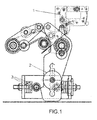
- the Figure 1 shows a latching-system according to the prior art.
- the additional mass is here a pendulum mass.
- the latching-system comprises a magnetic solenoid to pick up the coil 1, a pendulum mass 2 and a damper for pendulum 3.
- the operating mechanism for tripping a voltage circuit-breaker of the invention does not have such drawbacks.
- the invention relates to an operating mechanism for tripping a circuit-breaker, the operating mechanism comprising a coil having a first terminal and a second terminal, means for generating a first electric impulse, and means for creating, from the first electric impulse, a second electric impulse delayed from the first electric impulse and applied between the first terminal and the second terminal of the coil, characterised in that the means for creating the second electric impulse comprise a delaying circuit and a switch connected in series with the coil, the delaying circuit having an input connected to an output of the means for generating a first electric impulse and an output which delivers the second electric impulse, said second electric impulse being a command signal of the switch.
- the delaying circuit comprises a timer circuit having an input and an output, an integrating circuit and a driving circuit, the integrating circuit being connected at the input of the timer circuit and the first electric impulse being applied at the terminals of integrated circuit, and the driving circuit being connected at the output of the timer circuit and delivering the command signal of the switch as soon as a voltage at the input of the timer circuit reaches a trigger-level.
- the operating mechanism of the invention comprises an electronic component able to delay the electric impulse applied to the coil by the time required.
- the electronic component able to delay the electric impulse is integrated with the coil in a same component.
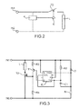
- the Figure 2 represents a diagram of an operating mechanism for tripping a voltage circuit breaker according to the invention.
- the operating mechanism comprises means for generating an electric impulse (not shown on the figure), means for delaying the electric impulse 4, T2 and a coil L.
- the means for delaying the electric impulse are a delaying circuit 4 and a switch T2.
- the delaying circuit 4 has a first input terminal IN1 connected to a first output of the means for generating the electric impulse, a second input terminal IN2 connected to a second output of the means for generating the electric impulse and an output terminal K connected to the input command of the switch T2.
- the coil L is in series with the switch T2.
- the switch T2 is OFF (open circuit) before the electric impulse is applied between the first terminal IN1 and the second terminal IN2.
- the delaying circuit 4 When the electric impulse is applied between the terminals IN1 and IN2, the delaying circuit 4 is powered on. When powered on, the delaying circuit 4 comprises means able to output, on the output terminal K, a pulse signal after a duration equal to the time-delay required. This pulse signal switches ON the switch T2 (short circuit) so that a magnetic force is created.
- the Figure 3 represents an example of the operating mechanism of the invention represented in Figure 2 .
- the operating mechanism comprises the resistors R1, R2, R3, R4, a timer circuit IC, a condenser C1, a diode D, a bipolar transistor T1 and the switch T2.
- the switch T2 is for example a field effect transistor.
- the coil L is in series with the transistor T2.
- the transistor T1 is in series with the resistors R3 and R4, a first terminal of the resistor R3 being connected to the emitter of the transistor T1 and a first terminal of the resistor R4 being connected to the collector of the transistor T1.
- the collector of the transistor T1 is connected to the gate of the transistor T2, which gate is the input command of the switch.
- the second terminal of the resistance R3 is connected to a first terminal of the coil L, the second terminal of which is connected to a first terminal of the switch T2, the second terminal of which is connected to the second terminal of the resistor R4.
- a first terminal of the resistor R2 is connected to a first terminal of the condenser C1, the second terminal of which is connected to a first terminal of the resistor R1.
- the second terminal of the resistor R2 is connected to the second terminal of the resistor R3 and the second terminal of the condencser C1 is connected to the second terminal of the resistor R4.
- the first terminal of the resistor R1 is also connected to a first terminal of the diode D1, the second terminal of which is connected to the second terminal of the resistor R2.
- the diode D and the resistor R1 are connected to the timer circuit IC so as to stabilize the supply-voltage of the timer circuit.
- the main elements allowing to delay the electric impulse are the timer circuit IC, the condenser C1 and the resistor R2.
- the first terminal of the condenser C1 is connected to an input TR of the timer-circuit IC.
- the gate of the transistor T1 is connected to an output Q of the timer circuit IC.
- the timer circuit IC When the electrical impulse is applied between the terminals IN1 and IN2, the timer circuit IC is powered on and, as long as the voltage at the input TR of the timer circuit is lower than a trigger-level, the output Q of the timer circuit IC stays at a logical level "high", keeping the transistor T1 closed. As soon as the trigger-level is reached at the input TR, the output Q turns to a logical level "low", opening thereby the transistor T1. Thus, the gate of the transistor T2 gets charged and the transistor T2 conducts. The coil L is therefore supplied. The transistor T1, together with the resistors R3 and R4 are to drive the transistor T2 from the logical signal output by the timer cicuit IC.
- the figure 4 represents an improvement of the example of means represented in Figure 3 .
- the operating mechanism represented in Figure 4 comprises a rectifier B placed between the terminals IN1 and IN2.
- This rectifier makes advantageously the circuit independent of polarity and suitable for active current AC and direct current DC.
Landscapes
- Physics & Mathematics (AREA)
- Electromagnetism (AREA)
- Driving Mechanisms And Operating Circuits Of Arc-Extinguishing High-Tension Switches (AREA)
- Keying Circuit Devices (AREA)
Abstract
Description
- The invention relates to an operating mechanism for tripping a voltage circuit-breaker and, more particularly, to an operating mechanism for tripping a high and medium voltage circuit-breaker.
- The energy to trip a voltage circuit-breaker is stored either in a spring (spring-operated mechanism) or in a hydraulic tank (hydraulic-operated mechanism). The spring is held in its charged position using a latching-system, while the hydraulic tank is kept under pressure by a closed valve. To trip the circuit-breaker, the latching-system or the valve is opened either manually or by a magnetic force created by a current flowing through a coil, the current resulting from an electric impulse applied to the coil.
- For some appications, the tripping time of the circuit-breaker has to be prolonged by several milliseconds to meet the requirements of the circuit-breaker.
- According to the prior art, an additional mass is attached to the latching-system of the mechanism. Due to the inertia of the additional mass, the tripping-time is delayed.
- The
Figure 1 shows a latching-system according to the prior art. The additional mass is here a pendulum mass. The latching-system comprises a magnetic solenoid to pick up thecoil 1, apendulum mass 2 and a damper forpendulum 3. - Such a mechanism has several drawbacks, i.e.:
- the system is position-dependent (the pendulum must be in vertical position to operate correctly, which presupposes that the mechanism must be fixed to the circuit-breaker in this unique position);
- the pendulum needs a lot of space, enlarging therefore the size of the mechanism;
- the latching-system comprises several mechanical parts, increasing thereby the cost of the mounting and the adjusting of the system;
- the different mechanical parts which constitute the latching-system are exposed to high accelerations and vibrations so that these parts can get loose and defective;
- the time-delay of the mechanical system is depending not only on its mass but also on the force acting to its latch so that adjusting the energy of the mechanism leads to another force on the latch and thus to a change in time-delay;
- the mass of the pendulum rises quadratically to the delay time so that using acceptable mass leads to a delay time limited to about 50 milliseconds.
- The operating mechanism for tripping a voltage circuit-breaker of the invention does not have such drawbacks.
- The invention relates to an operating mechanism for tripping a circuit-breaker, the operating mechanism comprising a coil having a first terminal and a second terminal, means for generating a first electric impulse, and means for creating, from the first electric impulse, a second electric impulse delayed from the first electric impulse and applied between the first terminal and the second terminal of the coil, characterised in that the means for creating the second electric impulse comprise a delaying circuit and a switch connected in series with the coil, the delaying circuit having an input connected to an output of the means for generating a first electric impulse and an output which delivers the second electric impulse, said second electric impulse being a command signal of the switch.
- According to another feature of the invention, the delaying circuit comprises a timer circuit having an input and an output, an integrating circuit and a driving circuit, the integrating circuit being connected at the input of the timer circuit and the first electric impulse being applied at the terminals of integrated circuit, and the driving circuit being connected at the output of the timer circuit and delivering the command signal of the switch as soon as a voltage at the input of the timer circuit reaches a trigger-level.
- The operating mechanism of the invention comprises an electronic component able to delay the electric impulse applied to the coil by the time required.
- According to a preferred embodiment of the invention, the electronic component able to delay the electric impulse is integrated with the coil in a same component.
- The operating mechanism of the invention has several advantages, i.e.:
- it is independent of the position of the drive,
- adjusting the energy of the mechanism does not influence the delay-time,
- the operating-mechanism of the invention has less mechanical parts than the operating-mechanism of the prior art, which is much more reliable and cost saving,
- the repeatability of a same delay-time is much more better than the one of the prior art,
- according to the preferred embodiment of the invention, there is no supplementary space needed in the mechanism because the means to delay the impulse is integrated with a coil in a same component.
- Other characteristics and advantages of the invention will become clearer upon reading a preferred embodiment of the invention made in reference to the attached figures, wherein:
- The
Figure 1 - already described - represents an operating mechanism for tripping a voltage circuit-breaker according to the prior art; - The
Figure 2 represents a diagram of an operating mechanism for tripping a voltage circuit breaker according to the invention; - The
Figure 3 represents an example of the operating mechanism of the invention represented inFigure 2 ; - The
figure 4 represents an improvement of the example of operating mechanism represented inFigure 3 . - In all the figures, the same references designate the same elements.
- The
Figure 2 represents a diagram of an operating mechanism for tripping a voltage circuit breaker according to the invention. - The operating mechanism comprises means for generating an electric impulse (not shown on the figure), means for delaying the electric impulse 4, T2 and a coil L. The means for delaying the electric impulse are a delaying circuit 4 and a switch T2.
- The delaying circuit 4 has a first input terminal IN1 connected to a first output of the means for generating the electric impulse, a second input terminal IN2 connected to a second output of the means for generating the electric impulse and an output terminal K connected to the input command of the switch T2.
- The coil L is in series with the switch T2. The switch T2 is OFF (open circuit) before the electric impulse is applied between the first terminal IN1 and the second terminal IN2.
- When the electric impulse is applied between the terminals IN1 and IN2, the delaying circuit 4 is powered on. When powered on, the delaying circuit 4 comprises means able to output, on the output terminal K, a pulse signal after a duration equal to the time-delay required. This pulse signal switches ON the switch T2 (short circuit) so that a magnetic force is created.
- The
Figure 3 represents an example of the operating mechanism of the invention represented inFigure 2 . - The operating mechanism comprises the resistors R1, R2, R3, R4, a timer circuit IC, a condenser C1, a diode D, a bipolar transistor T1 and the switch T2. The switch T2 is for example a field effect transistor.
- The coil L is in series with the transistor T2. The transistor T1 is in series with the resistors R3 and R4, a first terminal of the resistor R3 being connected to the emitter of the transistor T1 and a first terminal of the resistor R4 being connected to the collector of the transistor T1. The collector of the transistor T1 is connected to the gate of the transistor T2, which gate is the input command of the switch. The second terminal of the resistance R3 is connected to a first terminal of the coil L, the second terminal of which is connected to a first terminal of the switch T2, the second terminal of which is connected to the second terminal of the resistor R4. A first terminal of the resistor R2 is connected to a first terminal of the condenser C1, the second terminal of which is connected to a first terminal of the resistor R1. The second terminal of the resistor R2 is connected to the second terminal of the resistor R3 and the second terminal of the condencser C1 is connected to the second terminal of the resistor R4. The first terminal of the resistor R1 is also connected to a first terminal of the diode D1, the second terminal of which is connected to the second terminal of the resistor R2. The diode D and the resistor R1 are connected to the timer circuit IC so as to stabilize the supply-voltage of the timer circuit.
- The main elements allowing to delay the electric impulse are the timer circuit IC, the condenser C1 and the resistor R2. The first terminal of the condenser C1 is connected to an input TR of the timer-circuit IC. The gate of the transistor T1 is connected to an output Q of the timer circuit IC.
- When the electrical impulse is applied between the terminals IN1 and IN2, the timer circuit IC is powered on and, as long as the voltage at the input TR of the timer circuit is lower than a trigger-level, the output Q of the timer circuit IC stays at a logical level "high", keeping the transistor T1 closed. As soon as the trigger-level is reached at the input TR, the output Q turns to a logical level "low", opening thereby the transistor T1. Thus, the gate of the transistor T2 gets charged and the transistor T2 conducts. The coil L is therefore supplied. The transistor T1, together with the resistors R3 and R4 are to drive the transistor T2 from the logical signal output by the timer cicuit IC.
- It is therefore possible to set the time delay when an electric impulse is applied between the terminals of the coil.
- The
figure 4 represents an improvement of the example of means represented inFigure 3 . - In addition to the elements represented in
figure 3 , the operating mechanism represented inFigure 4 comprises a rectifier B placed between the terminals IN1 and IN2. This rectifier makes advantageously the circuit independent of polarity and suitable for active current AC and direct current DC.
Claims (3)
- Operating mechanism for tripping a circuit-breaker, the operating mechanism comprising a coil (L) having a first terminal and a second terminal, means for generating a first electric impulse, and means for creating, from the first electric impulse, a second electric impulse delayed from the first electric impulse and applied between the first terminal and the second terminal of the coil, characterised in that the means for creating the second electric impulse comprise a delaying circuit (4) and a switch (T2) connected in series with the coil (L), the delaying circuit (4) having an input connected to an output of the means for generating a first electric impulse and an output which delivers the second electric impulse, said second electric impulse being a command signal of the switch (T2).
- Operating mechanism according to claim 1, wherein the delaying circuit (4) comprises a timer circuit (IC) having an input and an output, an integrating circuit (R2, C1) and a driving circuit (R3, T1, R4), the integrating circuit being connected at the input of the timer circuit, the first electric impulse being applied at the terminals of integrated circuit, and the driving circuit being connected at the output of the timer circuit and delivering the command signal of the switch as soon as a voltage at the input of the timer circuit reaches a trigger-level.
- Operating mechanism according to claim 2, wherein the integrating circuit comprises a condenser (C1) at the terminals of which the first electric impulse is applied and the driving circuit comprises a PNP transistor (T1) the gate of which is connected to the output of the timer circuit and the collector of which is connected to an input command of the switch (T2).
Priority Applications (6)
| Application Number | Priority Date | Filing Date | Title |
|---|---|---|---|
| EP15153300.7A EP3051568B1 (en) | 2015-01-30 | 2015-01-30 | Operating mechanism for tripping a voltage circuit breaker |
| CA2974474A CA2974474A1 (en) | 2015-01-30 | 2016-01-28 | Operating mechanism for tripping a voltage circuit breaker |
| BR112017016214A BR112017016214A2 (en) | 2015-01-30 | 2016-01-28 | operating mechanism for tripping a circuit breaker |
| CN201680007832.3A CN107210147B (en) | 2015-01-30 | 2016-01-28 | Operating mechanism for tripping voltage circuit breakers |
| PCT/EP2016/051763 WO2016120364A1 (en) | 2015-01-30 | 2016-01-28 | Operating mechanism for tripping a voltage circuit breaker |
| US15/547,128 US20180005775A1 (en) | 2015-01-30 | 2016-01-28 | Operating mechanism for tripping a voltage circuit breaker |
Applications Claiming Priority (1)
| Application Number | Priority Date | Filing Date | Title |
|---|---|---|---|
| EP15153300.7A EP3051568B1 (en) | 2015-01-30 | 2015-01-30 | Operating mechanism for tripping a voltage circuit breaker |
Publications (2)
| Publication Number | Publication Date |
|---|---|
| EP3051568A1 true EP3051568A1 (en) | 2016-08-03 |
| EP3051568B1 EP3051568B1 (en) | 2019-03-13 |
Family
ID=52432733
Family Applications (1)
| Application Number | Title | Priority Date | Filing Date |
|---|---|---|---|
| EP15153300.7A Active EP3051568B1 (en) | 2015-01-30 | 2015-01-30 | Operating mechanism for tripping a voltage circuit breaker |
Country Status (6)
| Country | Link |
|---|---|
| US (1) | US20180005775A1 (en) |
| EP (1) | EP3051568B1 (en) |
| CN (1) | CN107210147B (en) |
| BR (1) | BR112017016214A2 (en) |
| CA (1) | CA2974474A1 (en) |
| WO (1) | WO2016120364A1 (en) |
Citations (2)
| Publication number | Priority date | Publication date | Assignee | Title |
|---|---|---|---|---|
| US3329870A (en) * | 1965-02-19 | 1967-07-04 | Square D Co | Static tripping device for an electric circuit breaker |
| WO2010102989A1 (en) * | 2009-03-10 | 2010-09-16 | Areva T&D Sas | Circuit for controlling an electromagnetic actuator for a vacuum switch |
Family Cites Families (1)
| Publication number | Priority date | Publication date | Assignee | Title |
|---|---|---|---|---|
| CN101673925B (en) * | 2008-09-12 | 2013-06-05 | 西门子公司 | Control device and control method for residual current circuit-breakers |
-
2015
- 2015-01-30 EP EP15153300.7A patent/EP3051568B1/en active Active
-
2016
- 2016-01-28 BR BR112017016214A patent/BR112017016214A2/en not_active Application Discontinuation
- 2016-01-28 CN CN201680007832.3A patent/CN107210147B/en active Active
- 2016-01-28 US US15/547,128 patent/US20180005775A1/en not_active Abandoned
- 2016-01-28 WO PCT/EP2016/051763 patent/WO2016120364A1/en not_active Ceased
- 2016-01-28 CA CA2974474A patent/CA2974474A1/en not_active Abandoned
Patent Citations (2)
| Publication number | Priority date | Publication date | Assignee | Title |
|---|---|---|---|---|
| US3329870A (en) * | 1965-02-19 | 1967-07-04 | Square D Co | Static tripping device for an electric circuit breaker |
| WO2010102989A1 (en) * | 2009-03-10 | 2010-09-16 | Areva T&D Sas | Circuit for controlling an electromagnetic actuator for a vacuum switch |
Also Published As
| Publication number | Publication date |
|---|---|
| US20180005775A1 (en) | 2018-01-04 |
| CN107210147A (en) | 2017-09-26 |
| CN107210147B (en) | 2019-10-18 |
| CA2974474A1 (en) | 2016-08-04 |
| BR112017016214A2 (en) | 2018-03-27 |
| WO2016120364A1 (en) | 2016-08-04 |
| EP3051568B1 (en) | 2019-03-13 |
Similar Documents
| Publication | Publication Date | Title |
|---|---|---|
| JP6291929B2 (en) | Semiconductor device | |
| CA2115665C (en) | Microprocessor watch-dog monitor for electronic trip units | |
| JPS61250310A (en) | Method and device for controlling gas exchange valve in internal combustion engine | |
| US10170257B2 (en) | Systems and methods for controlling relays | |
| EP1936650A1 (en) | Apparatus and method for controlling a solenoid | |
| RU2017129112A (en) | AUTOMATED CIRCUIT BREAKER CONTROLLER | |
| US10256065B2 (en) | Systems and methods for controlling relays | |
| US4763222A (en) | Vehicle suspension control with actuating circuit protection | |
| US7367302B2 (en) | Method and device for switching on a power switch arranged between capacitive elements | |
| US4402033A (en) | Sensitive relay with high threshold stability | |
| EP3051568B1 (en) | Operating mechanism for tripping a voltage circuit breaker | |
| US12424843B2 (en) | Systems and methods to protect a MEMS relay switch system | |
| US3382417A (en) | Time delay relay device | |
| EP2783381B1 (en) | A method and circuit for increasing the speed of an electromechanical output on a protective relay | |
| US10026574B2 (en) | Multi-load drive circuit | |
| US10305390B2 (en) | Filter circuit for eliminating inrush current, DC coil control circuit, and electromagnetic contactor | |
| JP7185768B2 (en) | relay module | |
| RU2707971C2 (en) | Electric relay device | |
| US12573573B2 (en) | Tripping device for a circuit breaker | |
| US6606233B1 (en) | Method and apparatus for immunizing a contactor circuit from the adverse effects of a derived power supply | |
| US2236981A (en) | Timing device | |
| SU594905A3 (en) | Electronic switch | |
| US3579043A (en) | Reverse power relay | |
| US2745024A (en) | Sensitive time delay relay | |
| JPH0443402B2 (en) |
Legal Events
| Date | Code | Title | Description |
|---|---|---|---|
| PUAI | Public reference made under article 153(3) epc to a published international application that has entered the european phase |
Free format text: ORIGINAL CODE: 0009012 |
|
| AK | Designated contracting states |
Kind code of ref document: A1 Designated state(s): AL AT BE BG CH CY CZ DE DK EE ES FI FR GB GR HR HU IE IS IT LI LT LU LV MC MK MT NL NO PL PT RO RS SE SI SK SM TR |
|
| AX | Request for extension of the european patent |
Extension state: BA ME |
|
| STAA | Information on the status of an ep patent application or granted ep patent |
Free format text: STATUS: REQUEST FOR EXAMINATION WAS MADE |
|
| 17P | Request for examination filed |
Effective date: 20161216 |
|
| RBV | Designated contracting states (corrected) |
Designated state(s): AL AT BE BG CH CY CZ DE DK EE ES FI FR GB GR HR HU IE IS IT LI LT LU LV MC MK MT NL NO PL PT RO RS SE SI SK SM TR |
|
| GRAP | Despatch of communication of intention to grant a patent |
Free format text: ORIGINAL CODE: EPIDOSNIGR1 |
|
| STAA | Information on the status of an ep patent application or granted ep patent |
Free format text: STATUS: GRANT OF PATENT IS INTENDED |
|
| INTG | Intention to grant announced |
Effective date: 20181112 |
|
| GRAS | Grant fee paid |
Free format text: ORIGINAL CODE: EPIDOSNIGR3 |
|
| GRAA | (expected) grant |
Free format text: ORIGINAL CODE: 0009210 |
|
| STAA | Information on the status of an ep patent application or granted ep patent |
Free format text: STATUS: THE PATENT HAS BEEN GRANTED |
|
| AK | Designated contracting states |
Kind code of ref document: B1 Designated state(s): AL AT BE BG CH CY CZ DE DK EE ES FI FR GB GR HR HU IE IS IT LI LT LU LV MC MK MT NL NO PL PT RO RS SE SI SK SM TR |
|
| REG | Reference to a national code |
Ref country code: GB Ref legal event code: FG4D |
|
| REG | Reference to a national code |
Ref country code: CH Ref legal event code: EP Ref country code: AT Ref legal event code: REF Ref document number: 1108842 Country of ref document: AT Kind code of ref document: T Effective date: 20190315 |
|
| REG | Reference to a national code |
Ref country code: IE Ref legal event code: FG4D |
|
| REG | Reference to a national code |
Ref country code: DE Ref legal event code: R096 Ref document number: 602015026156 Country of ref document: DE |
|
| REG | Reference to a national code |
Ref country code: CH Ref legal event code: NV Representative=s name: VALIPAT S.A. C/O BOVARD SA NEUCHATEL, CH |
|
| REG | Reference to a national code |
Ref country code: NL Ref legal event code: MP Effective date: 20190313 |
|
| REG | Reference to a national code |
Ref country code: LT Ref legal event code: MG4D |
|
| PG25 | Lapsed in a contracting state [announced via postgrant information from national office to epo] |
Ref country code: NO Free format text: LAPSE BECAUSE OF FAILURE TO SUBMIT A TRANSLATION OF THE DESCRIPTION OR TO PAY THE FEE WITHIN THE PRESCRIBED TIME-LIMIT Effective date: 20190613 Ref country code: LT Free format text: LAPSE BECAUSE OF FAILURE TO SUBMIT A TRANSLATION OF THE DESCRIPTION OR TO PAY THE FEE WITHIN THE PRESCRIBED TIME-LIMIT Effective date: 20190313 Ref country code: SE Free format text: LAPSE BECAUSE OF FAILURE TO SUBMIT A TRANSLATION OF THE DESCRIPTION OR TO PAY THE FEE WITHIN THE PRESCRIBED TIME-LIMIT Effective date: 20190313 Ref country code: FI Free format text: LAPSE BECAUSE OF FAILURE TO SUBMIT A TRANSLATION OF THE DESCRIPTION OR TO PAY THE FEE WITHIN THE PRESCRIBED TIME-LIMIT Effective date: 20190313 |
|
| PG25 | Lapsed in a contracting state [announced via postgrant information from national office to epo] |
Ref country code: LV Free format text: LAPSE BECAUSE OF FAILURE TO SUBMIT A TRANSLATION OF THE DESCRIPTION OR TO PAY THE FEE WITHIN THE PRESCRIBED TIME-LIMIT Effective date: 20190313 Ref country code: RS Free format text: LAPSE BECAUSE OF FAILURE TO SUBMIT A TRANSLATION OF THE DESCRIPTION OR TO PAY THE FEE WITHIN THE PRESCRIBED TIME-LIMIT Effective date: 20190313 Ref country code: BG Free format text: LAPSE BECAUSE OF FAILURE TO SUBMIT A TRANSLATION OF THE DESCRIPTION OR TO PAY THE FEE WITHIN THE PRESCRIBED TIME-LIMIT Effective date: 20190613 Ref country code: GR Free format text: LAPSE BECAUSE OF FAILURE TO SUBMIT A TRANSLATION OF THE DESCRIPTION OR TO PAY THE FEE WITHIN THE PRESCRIBED TIME-LIMIT Effective date: 20190614 Ref country code: NL Free format text: LAPSE BECAUSE OF FAILURE TO SUBMIT A TRANSLATION OF THE DESCRIPTION OR TO PAY THE FEE WITHIN THE PRESCRIBED TIME-LIMIT Effective date: 20190313 Ref country code: HR Free format text: LAPSE BECAUSE OF FAILURE TO SUBMIT A TRANSLATION OF THE DESCRIPTION OR TO PAY THE FEE WITHIN THE PRESCRIBED TIME-LIMIT Effective date: 20190313 |
|
| REG | Reference to a national code |
Ref country code: AT Ref legal event code: MK05 Ref document number: 1108842 Country of ref document: AT Kind code of ref document: T Effective date: 20190313 |
|
| PG25 | Lapsed in a contracting state [announced via postgrant information from national office to epo] |
Ref country code: PT Free format text: LAPSE BECAUSE OF FAILURE TO SUBMIT A TRANSLATION OF THE DESCRIPTION OR TO PAY THE FEE WITHIN THE PRESCRIBED TIME-LIMIT Effective date: 20190713 Ref country code: AL Free format text: LAPSE BECAUSE OF FAILURE TO SUBMIT A TRANSLATION OF THE DESCRIPTION OR TO PAY THE FEE WITHIN THE PRESCRIBED TIME-LIMIT Effective date: 20190313 Ref country code: ES Free format text: LAPSE BECAUSE OF FAILURE TO SUBMIT A TRANSLATION OF THE DESCRIPTION OR TO PAY THE FEE WITHIN THE PRESCRIBED TIME-LIMIT Effective date: 20190313 Ref country code: IT Free format text: LAPSE BECAUSE OF FAILURE TO SUBMIT A TRANSLATION OF THE DESCRIPTION OR TO PAY THE FEE WITHIN THE PRESCRIBED TIME-LIMIT Effective date: 20190313 Ref country code: RO Free format text: LAPSE BECAUSE OF FAILURE TO SUBMIT A TRANSLATION OF THE DESCRIPTION OR TO PAY THE FEE WITHIN THE PRESCRIBED TIME-LIMIT Effective date: 20190313 Ref country code: SK Free format text: LAPSE BECAUSE OF FAILURE TO SUBMIT A TRANSLATION OF THE DESCRIPTION OR TO PAY THE FEE WITHIN THE PRESCRIBED TIME-LIMIT Effective date: 20190313 Ref country code: CZ Free format text: LAPSE BECAUSE OF FAILURE TO SUBMIT A TRANSLATION OF THE DESCRIPTION OR TO PAY THE FEE WITHIN THE PRESCRIBED TIME-LIMIT Effective date: 20190313 Ref country code: EE Free format text: LAPSE BECAUSE OF FAILURE TO SUBMIT A TRANSLATION OF THE DESCRIPTION OR TO PAY THE FEE WITHIN THE PRESCRIBED TIME-LIMIT Effective date: 20190313 |
|
| PG25 | Lapsed in a contracting state [announced via postgrant information from national office to epo] |
Ref country code: SM Free format text: LAPSE BECAUSE OF FAILURE TO SUBMIT A TRANSLATION OF THE DESCRIPTION OR TO PAY THE FEE WITHIN THE PRESCRIBED TIME-LIMIT Effective date: 20190313 Ref country code: PL Free format text: LAPSE BECAUSE OF FAILURE TO SUBMIT A TRANSLATION OF THE DESCRIPTION OR TO PAY THE FEE WITHIN THE PRESCRIBED TIME-LIMIT Effective date: 20190313 |
|
| REG | Reference to a national code |
Ref country code: DE Ref legal event code: R097 Ref document number: 602015026156 Country of ref document: DE |
|
| PG25 | Lapsed in a contracting state [announced via postgrant information from national office to epo] |
Ref country code: IS Free format text: LAPSE BECAUSE OF FAILURE TO SUBMIT A TRANSLATION OF THE DESCRIPTION OR TO PAY THE FEE WITHIN THE PRESCRIBED TIME-LIMIT Effective date: 20190713 Ref country code: AT Free format text: LAPSE BECAUSE OF FAILURE TO SUBMIT A TRANSLATION OF THE DESCRIPTION OR TO PAY THE FEE WITHIN THE PRESCRIBED TIME-LIMIT Effective date: 20190313 |
|
| PLBE | No opposition filed within time limit |
Free format text: ORIGINAL CODE: 0009261 |
|
| STAA | Information on the status of an ep patent application or granted ep patent |
Free format text: STATUS: NO OPPOSITION FILED WITHIN TIME LIMIT |
|
| PG25 | Lapsed in a contracting state [announced via postgrant information from national office to epo] |
Ref country code: DK Free format text: LAPSE BECAUSE OF FAILURE TO SUBMIT A TRANSLATION OF THE DESCRIPTION OR TO PAY THE FEE WITHIN THE PRESCRIBED TIME-LIMIT Effective date: 20190313 |
|
| 26N | No opposition filed |
Effective date: 20191216 |
|
| PG25 | Lapsed in a contracting state [announced via postgrant information from national office to epo] |
Ref country code: SI Free format text: LAPSE BECAUSE OF FAILURE TO SUBMIT A TRANSLATION OF THE DESCRIPTION OR TO PAY THE FEE WITHIN THE PRESCRIBED TIME-LIMIT Effective date: 20190313 |
|
| PG25 | Lapsed in a contracting state [announced via postgrant information from national office to epo] |
Ref country code: TR Free format text: LAPSE BECAUSE OF FAILURE TO SUBMIT A TRANSLATION OF THE DESCRIPTION OR TO PAY THE FEE WITHIN THE PRESCRIBED TIME-LIMIT Effective date: 20190313 |
|
| PG25 | Lapsed in a contracting state [announced via postgrant information from national office to epo] |
Ref country code: MC Free format text: LAPSE BECAUSE OF FAILURE TO SUBMIT A TRANSLATION OF THE DESCRIPTION OR TO PAY THE FEE WITHIN THE PRESCRIBED TIME-LIMIT Effective date: 20190313 |
|
| GBPC | Gb: european patent ceased through non-payment of renewal fee |
Effective date: 20200130 |
|
| REG | Reference to a national code |
Ref country code: BE Ref legal event code: MM Effective date: 20200131 |
|
| PG25 | Lapsed in a contracting state [announced via postgrant information from national office to epo] |
Ref country code: LU Free format text: LAPSE BECAUSE OF NON-PAYMENT OF DUE FEES Effective date: 20200130 Ref country code: GB Free format text: LAPSE BECAUSE OF NON-PAYMENT OF DUE FEES Effective date: 20200130 Ref country code: FR Free format text: LAPSE BECAUSE OF NON-PAYMENT OF DUE FEES Effective date: 20200131 |
|
| PG25 | Lapsed in a contracting state [announced via postgrant information from national office to epo] |
Ref country code: BE Free format text: LAPSE BECAUSE OF NON-PAYMENT OF DUE FEES Effective date: 20200131 |
|
| PG25 | Lapsed in a contracting state [announced via postgrant information from national office to epo] |
Ref country code: IE Free format text: LAPSE BECAUSE OF NON-PAYMENT OF DUE FEES Effective date: 20200130 |
|
| PG25 | Lapsed in a contracting state [announced via postgrant information from national office to epo] |
Ref country code: MT Free format text: LAPSE BECAUSE OF FAILURE TO SUBMIT A TRANSLATION OF THE DESCRIPTION OR TO PAY THE FEE WITHIN THE PRESCRIBED TIME-LIMIT Effective date: 20190313 Ref country code: CY Free format text: LAPSE BECAUSE OF FAILURE TO SUBMIT A TRANSLATION OF THE DESCRIPTION OR TO PAY THE FEE WITHIN THE PRESCRIBED TIME-LIMIT Effective date: 20190313 |
|
| PG25 | Lapsed in a contracting state [announced via postgrant information from national office to epo] |
Ref country code: MK Free format text: LAPSE BECAUSE OF FAILURE TO SUBMIT A TRANSLATION OF THE DESCRIPTION OR TO PAY THE FEE WITHIN THE PRESCRIBED TIME-LIMIT Effective date: 20190313 |
|
| P01 | Opt-out of the competence of the unified patent court (upc) registered |
Effective date: 20230522 |
|
| REG | Reference to a national code |
Ref country code: CH Ref legal event code: U11 Free format text: ST27 STATUS EVENT CODE: U-0-0-U10-U11 (AS PROVIDED BY THE NATIONAL OFFICE) Effective date: 20260201 |
|
| PGFP | Annual fee paid to national office [announced via postgrant information from national office to epo] |
Ref country code: DE Payment date: 20251217 Year of fee payment: 12 |
|
| PGFP | Annual fee paid to national office [announced via postgrant information from national office to epo] |
Ref country code: CH Payment date: 20260201 Year of fee payment: 12 |