EP3051528A1 - Method of compensating image information and image information compensation device - Google Patents
Method of compensating image information and image information compensation device Download PDFInfo
- Publication number
- EP3051528A1 EP3051528A1 EP15187582.0A EP15187582A EP3051528A1 EP 3051528 A1 EP3051528 A1 EP 3051528A1 EP 15187582 A EP15187582 A EP 15187582A EP 3051528 A1 EP3051528 A1 EP 3051528A1
- Authority
- EP
- European Patent Office
- Prior art keywords
- average current
- pixel
- information
- display panel
- current
- Prior art date
- Legal status (The legal status is an assumption and is not a legal conclusion. Google has not performed a legal analysis and makes no representation as to the accuracy of the status listed.)
- Ceased
Links
Images






Classifications
-
- G—PHYSICS
- G09—EDUCATION; CRYPTOGRAPHY; DISPLAY; ADVERTISING; SEALS
- G09G—ARRANGEMENTS OR CIRCUITS FOR CONTROL OF INDICATING DEVICES USING STATIC MEANS TO PRESENT VARIABLE INFORMATION
- G09G3/00—Control arrangements or circuits, of interest only in connection with visual indicators other than cathode-ray tubes
- G09G3/20—Control arrangements or circuits, of interest only in connection with visual indicators other than cathode-ray tubes for presentation of an assembly of a number of characters, e.g. a page, by composing the assembly by combination of individual elements arranged in a matrix no fixed position being assigned to or needed to be assigned to the individual characters or partial characters
- G09G3/22—Control arrangements or circuits, of interest only in connection with visual indicators other than cathode-ray tubes for presentation of an assembly of a number of characters, e.g. a page, by composing the assembly by combination of individual elements arranged in a matrix no fixed position being assigned to or needed to be assigned to the individual characters or partial characters using controlled light sources
- G09G3/30—Control arrangements or circuits, of interest only in connection with visual indicators other than cathode-ray tubes for presentation of an assembly of a number of characters, e.g. a page, by composing the assembly by combination of individual elements arranged in a matrix no fixed position being assigned to or needed to be assigned to the individual characters or partial characters using controlled light sources using electroluminescent panels
- G09G3/32—Control arrangements or circuits, of interest only in connection with visual indicators other than cathode-ray tubes for presentation of an assembly of a number of characters, e.g. a page, by composing the assembly by combination of individual elements arranged in a matrix no fixed position being assigned to or needed to be assigned to the individual characters or partial characters using controlled light sources using electroluminescent panels semiconductive, e.g. using light-emitting diodes [LED]
- G09G3/3208—Control arrangements or circuits, of interest only in connection with visual indicators other than cathode-ray tubes for presentation of an assembly of a number of characters, e.g. a page, by composing the assembly by combination of individual elements arranged in a matrix no fixed position being assigned to or needed to be assigned to the individual characters or partial characters using controlled light sources using electroluminescent panels semiconductive, e.g. using light-emitting diodes [LED] organic, e.g. using organic light-emitting diodes [OLED]
- G09G3/3275—Details of drivers for data electrodes
- G09G3/3283—Details of drivers for data electrodes in which the data driver supplies a variable data current for setting the current through, or the voltage across, the light-emitting elements
-
- G—PHYSICS
- G09—EDUCATION; CRYPTOGRAPHY; DISPLAY; ADVERTISING; SEALS
- G09G—ARRANGEMENTS OR CIRCUITS FOR CONTROL OF INDICATING DEVICES USING STATIC MEANS TO PRESENT VARIABLE INFORMATION
- G09G3/00—Control arrangements or circuits, of interest only in connection with visual indicators other than cathode-ray tubes
- G09G3/20—Control arrangements or circuits, of interest only in connection with visual indicators other than cathode-ray tubes for presentation of an assembly of a number of characters, e.g. a page, by composing the assembly by combination of individual elements arranged in a matrix no fixed position being assigned to or needed to be assigned to the individual characters or partial characters
- G09G3/2003—Display of colours
-
- G—PHYSICS
- G09—EDUCATION; CRYPTOGRAPHY; DISPLAY; ADVERTISING; SEALS
- G09G—ARRANGEMENTS OR CIRCUITS FOR CONTROL OF INDICATING DEVICES USING STATIC MEANS TO PRESENT VARIABLE INFORMATION
- G09G3/00—Control arrangements or circuits, of interest only in connection with visual indicators other than cathode-ray tubes
- G09G3/20—Control arrangements or circuits, of interest only in connection with visual indicators other than cathode-ray tubes for presentation of an assembly of a number of characters, e.g. a page, by composing the assembly by combination of individual elements arranged in a matrix no fixed position being assigned to or needed to be assigned to the individual characters or partial characters
- G09G3/22—Control arrangements or circuits, of interest only in connection with visual indicators other than cathode-ray tubes for presentation of an assembly of a number of characters, e.g. a page, by composing the assembly by combination of individual elements arranged in a matrix no fixed position being assigned to or needed to be assigned to the individual characters or partial characters using controlled light sources
- G09G3/30—Control arrangements or circuits, of interest only in connection with visual indicators other than cathode-ray tubes for presentation of an assembly of a number of characters, e.g. a page, by composing the assembly by combination of individual elements arranged in a matrix no fixed position being assigned to or needed to be assigned to the individual characters or partial characters using controlled light sources using electroluminescent panels
- G09G3/32—Control arrangements or circuits, of interest only in connection with visual indicators other than cathode-ray tubes for presentation of an assembly of a number of characters, e.g. a page, by composing the assembly by combination of individual elements arranged in a matrix no fixed position being assigned to or needed to be assigned to the individual characters or partial characters using controlled light sources using electroluminescent panels semiconductive, e.g. using light-emitting diodes [LED]
- G09G3/3208—Control arrangements or circuits, of interest only in connection with visual indicators other than cathode-ray tubes for presentation of an assembly of a number of characters, e.g. a page, by composing the assembly by combination of individual elements arranged in a matrix no fixed position being assigned to or needed to be assigned to the individual characters or partial characters using controlled light sources using electroluminescent panels semiconductive, e.g. using light-emitting diodes [LED] organic, e.g. using organic light-emitting diodes [OLED]
-
- G—PHYSICS
- G09—EDUCATION; CRYPTOGRAPHY; DISPLAY; ADVERTISING; SEALS
- G09G—ARRANGEMENTS OR CIRCUITS FOR CONTROL OF INDICATING DEVICES USING STATIC MEANS TO PRESENT VARIABLE INFORMATION
- G09G2320/00—Control of display operating conditions
- G09G2320/02—Improving the quality of display appearance
- G09G2320/0233—Improving the luminance or brightness uniformity across the screen
-
- G—PHYSICS
- G09—EDUCATION; CRYPTOGRAPHY; DISPLAY; ADVERTISING; SEALS
- G09G—ARRANGEMENTS OR CIRCUITS FOR CONTROL OF INDICATING DEVICES USING STATIC MEANS TO PRESENT VARIABLE INFORMATION
- G09G2320/00—Control of display operating conditions
- G09G2320/02—Improving the quality of display appearance
- G09G2320/0271—Adjustment of the gradation levels within the range of the gradation scale, e.g. by redistribution or clipping
-
- G—PHYSICS
- G09—EDUCATION; CRYPTOGRAPHY; DISPLAY; ADVERTISING; SEALS
- G09G—ARRANGEMENTS OR CIRCUITS FOR CONTROL OF INDICATING DEVICES USING STATIC MEANS TO PRESENT VARIABLE INFORMATION
- G09G2320/00—Control of display operating conditions
- G09G2320/02—Improving the quality of display appearance
- G09G2320/0271—Adjustment of the gradation levels within the range of the gradation scale, e.g. by redistribution or clipping
- G09G2320/0276—Adjustment of the gradation levels within the range of the gradation scale, e.g. by redistribution or clipping for the purpose of adaptation to the characteristics of a display device, i.e. gamma correction
-
- G—PHYSICS
- G09—EDUCATION; CRYPTOGRAPHY; DISPLAY; ADVERTISING; SEALS
- G09G—ARRANGEMENTS OR CIRCUITS FOR CONTROL OF INDICATING DEVICES USING STATIC MEANS TO PRESENT VARIABLE INFORMATION
- G09G2320/00—Control of display operating conditions
- G09G2320/04—Maintaining the quality of display appearance
- G09G2320/043—Preventing or counteracting the effects of ageing
- G09G2320/048—Preventing or counteracting the effects of ageing using evaluation of the usage time
-
- G—PHYSICS
- G09—EDUCATION; CRYPTOGRAPHY; DISPLAY; ADVERTISING; SEALS
- G09G—ARRANGEMENTS OR CIRCUITS FOR CONTROL OF INDICATING DEVICES USING STATIC MEANS TO PRESENT VARIABLE INFORMATION
- G09G2320/00—Control of display operating conditions
- G09G2320/06—Adjustment of display parameters
- G09G2320/0673—Adjustment of display parameters for control of gamma adjustment, e.g. selecting another gamma curve
-
- G—PHYSICS
- G09—EDUCATION; CRYPTOGRAPHY; DISPLAY; ADVERTISING; SEALS
- G09G—ARRANGEMENTS OR CIRCUITS FOR CONTROL OF INDICATING DEVICES USING STATIC MEANS TO PRESENT VARIABLE INFORMATION
- G09G2330/00—Aspects of power supply; Aspects of display protection and defect management
- G09G2330/02—Details of power systems and of start or stop of display operation
- G09G2330/021—Power management, e.g. power saving
-
- G—PHYSICS
- G09—EDUCATION; CRYPTOGRAPHY; DISPLAY; ADVERTISING; SEALS
- G09G—ARRANGEMENTS OR CIRCUITS FOR CONTROL OF INDICATING DEVICES USING STATIC MEANS TO PRESENT VARIABLE INFORMATION
- G09G2360/00—Aspects of the architecture of display systems
- G09G2360/16—Calculation or use of calculated indices related to luminance levels in display data
Definitions
- the invention relates to a method of determining average current and a method of compensating image information, and an image information compensation device.
- a method for extracting average current includes calculating an on-pixel ratio based on gamma information corresponding to image information, the on-pixel ratio based on turned-on pixels of a plurality of pixels in a display panel; providing maximum current information based on a dimming level; calculating an average current of the display panel based on the on-pixel ratio and the maximum current information; and providing pixel average current information for each of the pixels, the pixel average current information determined based on the average current of the display panel.
- the pixel average current information may be determined based on a pixel average current look-up table.
- the method may include updating the pixel average current information in the pixel average current look-up table at a predetermined time interval.
- the predetermined time interval may be a predetermined frame interval. After the predetermined frame interval, the pixel average current information may not be updated when a current of a corresponding one of the pixels is o. After the predetermined frame interval, the pixel average current information may be updated when a current of a corresponding one of the pixels is not o.
- the method may include storing the maximum current information corresponding to the dimming level in a max current look-up table.
- the method may include increasing a maximum current value corresponding to the maximum current information as the dimming level decreases.
- the method may include storing the maximum current information corresponding to the dimming level in the maximum current look-up table before the display panel operates.
- An average current of the display panel may be less than or equal to a maximum current value corresponding to the maximum current information.
- the method may include increasing the average current of the display panel as the on-pixel ratio increases.
- the method may include increasing the average current of the display panel as the maximum current value corresponding to the maximum current information increases.
- the method may include determining the average current of the display panel based on a value obtained by multiplying the on-pixel ratio and the maximum current value corresponding to the maximum current information.
- the method may include calculating a light emitting area of the display panel; and changing the pixel average current look-up table based on the light emitting area of the display panel. Deviation among the pixel average current information for the pixels may be directly proportional to the light emitting area of the display panel.
- a method for compensating image information includes calculating an on-pixel ratio based on gamma information corresponding to image information, the on-pixel ratio based on turned-on pixels among a plurality of pixels in a display panel; providing maximum current information corresponding to a dimming level; calculating an average current of the display panel based on the on-pixel ratio and the maximum current information; determining pixel average current information for each of the pixels based on the average current of the display panel; and compensating the gamma information corresponding to the image information based on the pixel average current information for each of the pixels.
- the method may include generating a compensation constant for compensating the gamma information based on the pixel average current information for each of the pixels.
- the method may include storing the pixel average current information for each of the pixels in a pixel average current look-up table; and updating the pixel average current information in the pixel average current look-up table at a predetermined time interval.
- the method may include storing the maximum current information corresponding to the dimming level in a maximum current look-up table, and increasing a maximum current value corresponding to the maximum current information as the dimming level decreases.
- an apparatus includes an on-pixel calculator to calculate an on-pixel ratio based on gamma information corresponding to image information, the on-pixel ratio based on turned-on pixels among a plurality of in a display panel; a maximum current information provider to provide maximum current information corresponding to a dimming level; an average current calculator to calculate an average current of the display panel based on the on-pixel ratio and the maximum current information; and a pixel information provider to provide pixel average current information for each of the pixels, the pixel average current information determined based on the average current of the display panel.
- an image information compensation device comprising an on-pixel ratio calculation unit for calculating an on-pixel ratio based on gamma information corresponding to image information, the on-pixel ratio comprising the ratio of turned-on pixels to the total of turned-on and turned-off pixels in a display panel, a maximum current information providing unit for providing a maximum current value, an average current calculation unit for calculating the average current of the display panel from the on-pixel ratio and the provided maximum current value, a pixel average current information providing unit for providing pixel average current information for each of the pixels corresponding to the average current of the display panel and a gamma information compensation unit for generating compensated values of gamma information using the pixel average current information.
- an average current extraction (determination) device 10 includes an on-pixel calculation unit 100, a max current information providing unit 300, an average current calculation unit 500 and a pixel information providing unit 200.
- the on-pixel calculation unit 100 calculates an on-pixel ratio OPR using, for example, gamma information GI corresponding to image information IMI (S100).
- the on-pixel ratio OPR corresponds to turned-on pixels in a display panel DP.
- the pixels in the display panel DP may be turned-on based on the gamma information GI corresponding to the image information IMI.
- the on-pixel ratio OPR is 1 or 100%.
- the on-pixel ratio OPR is 0.5 or 50%.
- the on-pixel ratio OPR is 0.75 or 75%.
- the max current information providing unit 300 provides max current information MCI corresponding to a dimming level DL (S110).
- the max current information MCI may be, for example, a max current MC corresponding to the dimming level DL.
- the max current information MCI of the display panel DP may be changed according to the dimming level DL of the display device including the display panel DP. As the dimming level DL decreases, the max current MC corresponding to the max current information MCI of the display panel DP may increase. For example, when dimming level DL of the display device including the display panel DP is 3, the max current MC corresponding to the max current information MCI of the display panel DP may be 10. When the dimming level DL is 1, the max current MC corresponding to the max current information MCI of the display panel DP may be 100.
- the average current calculation unit 500 calculates an average current DAI of the display panel DP based on the on-pixel ratio OPR and the max current information MCI (S120).
- the average current DAI of the display panel DP may be a value based on multiplying the on-pixel ratio OPR and the max current MC value corresponding to the max current information MCI.
- the on-pixel ratio OPR may be 1 and the dimming level DL may be 1.
- the dimming level DL is 1
- the max current MC corresponding to the max current information MCI may be 100.
- the average current DAI of the display panel DP is 100, which is the value obtained by multiplying the on-pixel ratio OPR and the max current MC value.
- the on-pixel ratio OPR may be 0.5 and the dimming level DL may be 1.
- the dimming level DL is 1, the max current MC corresponding to the max current information MCI is 100.
- the average current DAI of the display panel DP is 50, which is the value obtained by multiplying the on-pixel ratio OPR and the max current MC value.
- the on-pixel ratio OPR may be 0.5 and the dimming level DL may be 3.
- the dimming level DL is 3
- the max current MC corresponding to the max current information MCI may be 10.
- the average current DAI of the display panel DP is 5, which is the value obtained by multiplying the on-pixel ratio OPR and the max current MC value.
- the pixel information providing unit 200 provides pixel average current information PAI for each of the pixels (S130).
- the pixel average current information PAI is determined by the average current DAI of the display panel DP.
- the pixel average current PAC for each of the pixels may be changed according to the average current DAI of the display panel DP.
- the pixel average current PAC for each of the pixels in the display panel DP may be determined.
- the pixel average current information PAI for each of the pixels in the display panel DP may be stored in a pixel average current look-up table PACLT.
- the method for extracting average current may compensate the image degradation of the display panel DP by providing the pixel average current information PAI for each of the pixels based on the average current DAI of the display panel DP.
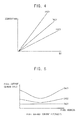
- FIGS. 3 and 4 illustrate examples for describing degradation based on pixel average current PAC.
- a transistor 75 when a transistor 75 is turned-on based on the data voltage DV, current is transferred through an organic light-emitting diode 76.
- the degree of degradation of the pixel may be different according to the pixel average current PAC transferred through the organic light-emitting diode 76.
- the pixel average current PAC transferred through the organic light-emitting diode 76 may be a first pixel average current PAC1.
- the pixel average current PAC transferred through the organic light-emitting diode 76 may be a second pixel average current PAC2.
- the pixel average current PAC transferred through the organic light-emitting diode 76 may be a third pixel average current PAC3.
- the first pixel average current PAC1 may be greater than the second pixel average current PAC2.
- the second pixel average current PAC2 may be greater than the third pixel average current PAC3.
- the degree of degradation of the pixel may increase as the pixel average current PAC transferred through the organic light-emitting diode 76 increases. For example, when the pixel average current PAC transferred through the organic light-emitting diode 76 is the first pixel average current PAC1, the degree of degradation of the pixel may be highest. When the pixel average current PAC transferred through the organic light-emitting diode 76 is the second pixel average current PAC2, the degree of degradation of the pixel may be second highest. When the pixel average current PAC transferred through the organic light-emitting diode 76 is the third pixel average current PAC3, the degree of degradation of the pixel may be lowest. The degree of degradation of the pixel may be different according to the pixel average current PAC transferred through the organic light-emitting diode 76.
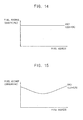
- FIG. 5 illustrates an example corresponding to a pixel average current look-up table.
- the pixel average current PAC for each of the pixels may be changed according to the average current DAI of the display panel DP.
- the pixel average current PAC for each of the pixels in the display panel DP may be determined.
- the pixel average current information PAI for each of the pixels in the display panel DP may be stored in a pixel average current look-up table PACLT.
- the average current DAI of the display panel DP may be a first average current DAC1.
- the pixel average current PAC may be increased after the pixel average current PAC is decreased.
- the average current DAI of the display panel DP may be a second average current DAC2.
- the pixel average current PAC may be increased after the pixel average current PAC is decreased.
- the range of the pixel average current PAC in the second average current DAC2 may be less than the range of the pixel average current PAC in the first average current DAC1.
- the average current DAI of the display panel DP may be a third average current DAC3. In this case, as the pixel address is increased, the pixel average current PAC may be constant.
- the pixel average current information PAI for each of the pixels according to the average current DAI of the display panel DP may be stored in a pixel average current look-up table PACLT.
- the pixel information providing unit 200 may include the pixel average current look-up table PACLT for storing pixel average current information PAI for each of the pixels.
- the method for extracting average current may compensate image degradation of the display panel DP by providing the pixel average current information PAI for each of the pixels based on the average current DAI of the display panel DP.
- FIG. 6 illustrates an example for updating pixel average current in the pixel average current look-up table PACLT.
- the pixel average current information PAI in the pixel average current look-up table PACLT may be updated at predetermined time intervals PDT.
- the average current extraction device 10 may update the pixel average current information PAI in the pixel average current look-up table PACLT based on a first pixel current PC1.
- the first pixel current PC1 may be a current transferred to the organic light-emitting diode 76 in the first time T1.
- the average current extraction device 10 may update the pixel average current information PAI in the pixel average current look-up table PACLT based on a second pixel current PC2.
- the second pixel current PC2 may be a current transferred to the organic light-emitting diode 76 in the second time T2.
- the average current extraction device 10 may update the pixel average current information PAI in the pixel average current look-up table PACLT based on a third pixel current PC.
- the third pixel current PC may be a current transferred to the organic light-emitting diode 76 in the third time T3.
- the time interval between the first time T1 and the second time T2 may be the predetermined time interval PDT.
- the time interval between the second time T2 and the third time T3 may be the predetermined time interval PDT. These intervals may be different in another embodiment.
- the method for extracting average current may compensate image degradation of the display panel DP by providing the pixel average current information PAI for each of the pixels based on the average current DAI of the display panel DP.
- FIGS. 7 and 8 illustrate additional examples for updating pixel average current information in a pixel average current look-up table.
- the predetermined time interval PDT may be a predetermined frame interval.
- the pixel average current look-up table PACLT may be updated.
- the predetermined frame interval when a current of the pixel is 0, the pixel average current information PAI for the pixel may not be updated.
- the predetermined frame interval may be one frame interval.
- the first pixel current PC1 transferred to the organic light-emitting diode 76 in the first pixel PIXEL1 may be 5.
- the first pixel average current PAC1 may be 5.
- the pixel average current information PAI corresponding to the first pixel average current PAC1 in the pixel average current look-up table PACLT may be updated to 5.
- the second pixel current PC2 transferred to the organic light-emitting diode 76 in the first pixel PIXEL1 may be o.
- the second pixel average current PAC2 may be 5. After the predetermined frame interval, when the current of the pixel is 0, the pixel average current information PAI for the pixel may not be updated.
- the pixel average current look-up table PACLT may be updated. After the predetermined frame interval, if the current of the pixel is not 0, the pixel average current information PAI for the pixel may be updated.
- the third pixel current PC transferred to the organic light-emitting diode 76 in the first pixel PIXEL1 may be 4.
- the pixel average current information PAI corresponding to the third pixel average current PAC3 in the pixel average current look-up table PACLT may be updated to 3.
- the pixel average current information PAI for the first pixel PIXEL1 may be updated to 5 in the first frame F1.
- the pixel average current information PAI for the first pixel PIXEL1 may not be updated in the second frame F2.
- the pixel average current information PAI for the first pixel PIXEL1 may be updated to 3 in the third frame F3.
- the method for extracting average current may compensate image degradation of the display panel DP by providing the pixel average current information PAI for each of the pixels based on the average current of the display panel DP.
- FIG. 9 illustrates an example of a max current look-up table
- FIG. 10 illustrates an example for describing a max current value corresponding to max current info.
- the max current information providing unit 300 may include a max current look-up table MCLT that stores the max current information MCI corresponding to the dimming level DL.
- the max current information MCI corresponding to the dimming level DL may be stored in the max current look-up table MCLT before the display panel DP operates. As the dimming level DL is decreased, a max current MC value corresponding to the max current information MCI may be increased.
- the max current MC corresponding to the max current information MCI may be 100.
- the max current MC corresponding to the max current information MCI may be 50.
- the max current MC corresponding to the max current information MCI may be 10.
- the dimming level DL of the display device including the average current extraction device 10 is 3
- the max current MC corresponding to the max current information MCI may be o.
- a max current value corresponding to the max current information MCI may be increased.
- the max current MC corresponding to the max current information MCI may be used to calculate the average current DAI of the display panel DP.
- the on-pixel ratio OPR may be 1.
- the dimming level DL of the display device is 1, the max current MC corresponding to the max current information MCI may be 50. In this case, the average current DAI of the display panel DP may be 50.
- the dimming level DL of the display device is 2, the max current MC corresponding to the max current information MCI may be 10. In this case, the average current DAI of the display panel DP may be 10.
- the dimming level DL of the display device is 3
- the max current MC corresponding to the max current information MCI may be o. In this case, the average current DAI of the display panel DP may be o.
- FIGS. 11 and 12 illustrate examples for describing average current of a display panel according to an on-pixel ratio.
- an average current DAI of the display panel DP may be less than or equal to a max current MC value corresponding to the max current information MCI.
- the on-pixel ratio OPR is 1, the average current DAI of the display panel DP may be equal to the max current MC corresponding to the max current information MCI.
- the on-pixel ratio OPR is less than 1
- the average current DAI of the display panel DP may be less than the max current MC corresponding to the max current information MCI.
- the average current DAI of the display panel DP may be increased.
- the dimming level DL of the display device is 0
- the on-pixel ratio OPR is 0.5
- the average current DAI of the display panel DP may be 50.
- the dimming level DL of the display device is 3 and the on-pixel ratio OPR is 0.75
- the average current DAI of the display panel DP may be 75. Therefore, as the on-pixel ratio OPR is increased, the average current DAI of the display panel DP is increased.
- the average current DAI of the display panel DP may be increased.
- the on-pixel ratio OPR may be 0.5 and the dimming level DL may be 1.
- the dimming level DL is 1, the max current MC corresponding to the max current information MCI may be 50.
- the average current DAI of the display panel DP may be 25.
- the on-pixel ratio OPR may be 0.5 and the dimming level DL may be 2.
- the dimming level DL is 2
- the max current MC corresponding to the max current information MCI may be 10.
- the average current DAI of the display panel DP may be 5.
- the on-pixel ratio OPR may be 0.5 and the dimming level DL may be o.
- the max current MC corresponding to the max current information MCI may be 100.
- the average current DAI of the display panel DP may be 50.
- the average current DAI of the display panel DP may be a value obtained by multiplying the on-pixel ratio OPR and the max current MC value corresponding to the max current information MCI.
- the method for extracting average current may compensate image degradation of the display panel DP by providing the pixel average current information PAI for each of the pixels based on the average current DAI of the display panel DP.
- FIG. 13 illustrates another embodiment of an average current extraction device
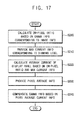
- FIGS. 14 to 16 illustrate examples corresponding to a pixel average current look-up table according to a light emitting area.
- an average current extraction device 10a includes an on-pixel calculation unit 100, a max current information providing unit 300, an average current calculation unit 500, and a pixel information providing unit 200.
- the on-pixel calculation unit 100 calculates an on-pixel ratio OPR based on a gamma information GI corresponding to image information IMI.
- the on-pixel ratio OPR corresponds to turned-on pixels among pixels in a display panel DP.
- a max current information providing unit 300 provides a max current information MCI corresponding to a dimming level DL.
- the average current calculation unit 500 calculates an average current of the display panel DP based on the on-pixel ratio OPR and the max current information MCI.
- the pixel information providing unit 200 provides a pixel average current information PAI for each of the pixels.
- the pixel average current information PAI is determined by the average current DAI of the display panel DP.
- a display device including the display panel DP may include a light emitting area calculator 400 to calculate a light emitting area LEA of the display panel DP.
- the pixel information providing unit 200 may change the pixel average current look-up table PACLT based on the light emitting area LEA of the display panel DP.
- the average current DAI of the display panel DP may be the first average current DAC1.
- the pixel average current look-up table PACLT according to the light emitting area LEA may be generated based on the curve for the first average current DAC1 of FIG. 5 .
- the pixel average current look-up table PACLT may be similar to the curve for the first average current DAC1 of FIG. 5 .
- the range of the pixel average current PAC value corresponding to the pixel average current information PAI stored in the pixel average current look-up table PACLT may be decreased.
- a deviation among the pixel average current information PAI for the pixels may be decreased.
- the pixel average current look-up table PACLT may be separately generated for each of the light emitting areas.
- the method for extracting average current may compensate image degradation of the display panel DP by providing the pixel average current information PAI for each of the pixels based on the average current DAI of the display panel DP.
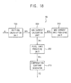
- FIG. 17 illustrates an embodiment of a method for compensating image information
- FIG. 18 illustrates an embodiment of an image information compensation device 15.
- the image information compensation device 15 includes an on-pixel calculation unit 100, a max current information providing unit 300, an average current calculation unit 500, a pixel information providing unit 200 and a compensation constant generator 210.
- the on-pixel calculation unit 100 calculates an on-pixel ratio OPR based on a gamma information GI corresponding to image information IMI (S200).
- the on-pixel ratio OPR corresponds to turned-on pixels among pixels in the display panel DP.
- the on-pixel ratio OPR corresponds to turned-on pixels among pixels included in a display panel DP.
- the pixels in the display panel DP may be turned-on based the gamma information GI corresponding to the image information IMI.
- the on-pixel ratio OPR may be 1 or 100%.
- the on-pixel ratio OPR may be 0.5 or 50%.
- the on-pixel ratio OPR may be 0.75 or 75%.
- the max current information providing unit 300 provides a max current information MCI corresponding to a dimming level DL (S210).
- the max current information MCI may be a max current MC value corresponding to the dimming level DL.
- the max current information MCI of the display panel DP may be changed according to the dimming level DL of the display device including the display panel DP. As the dimming level DL is decreased, the max current MC corresponding to the max current information MCI of the display panel DP may be increased. For example, when the dimming level DL is 1, the max current MC corresponding to the max current information MCI of the display panel DP may be 50. When the dimming level DL is 3, the max current MC corresponding to the max current information MCI of the display panel DP may be o.
- the average current calculation unit 500 calculates an average current DAI of the display panel DP based on the on-pixel ratio OPR and the max current information MCI (S220).
- the average current DAI may be a value obtained by multiplying the on-pixel ratio OPR and the max current MC value corresponding to the max current information MCI.
- the on-pixel ratio OPR may be 1 and the dimming level DL may be 1.
- the dimming level DL is 1, the max current MC corresponding to the max current information MCI may be 50.
- the average current DAI of the display panel DP may be 50.
- the value obtained by multiplying the on-pixel ratio OPR and the max current MC value corresponding to the max current information MCI may be 50.
- the on-pixel ratio OPR may be 0.5 and the dimming level DL may be 1.
- the dimming level DL is 1, the max current MC corresponding to the max current information MCI may be 50.
- the average current DAI of the display panel DP may be 25.
- the value obtained by multiplying the on-pixel ratio OPR and the max current MC value corresponding to the max current information MCI may be 25.
- the on-pixel ratio OPR may be 0.5 and the dimming level DL may be o.
- the dimming level DL is 0, the max current MC corresponding to the max current information MCI may be 100.
- the average current DAI of the display panel DP may be 50.
- the value obtained by multiplying the on-pixel ratio OPR and the max current MC value corresponding to the max current information MCI may be 50.
- the pixel information providing unit 200 provides a pixel average current information PAI for each of the pixels (S230).
- the pixel average current information PAI is determined by the average current DAI of the display panel DP.
- the pixel average current PAC for each of the pixels may be changed according to the average current DAI of the display panel DP.
- the pixel average current PAC for each of the pixels in the display panel DP may be determined.
- the pixel average current information PAI for each of the pixels in the display panel DP may be stored in a pixel average current look-up table PACLT.
- the gamma information GI corresponding to the image information IMI is compensated based on the pixel average current information PAI for each of the pixels (S240).
- a display device including the display panel DP may include a compensation constant generator 210 that generates a compensation constant CC of compensating the gamma information GI based on the pixel average current information PAI for each of the pixels.
- the gamma information GI corresponding to the image information IMI may be compensated using the compensation constant CC generated from the compensation constant generator 210.
- the compensation constant CC may be applied to a data voltage to compensate the data voltage.
- the pixel information providing unit 200 includes a pixel average current look-up table PACLT that stores the pixel average current information PAI for each of the pixels.
- the pixel average current information PAI in the pixel average current look-up table PACLT may be updated every a predetermined time interval PDT.
- the pixel average current PAC for each of the pixels may be changed according to the average current DAI of the display panel DP.
- the pixel average current PAC for each of the pixels in the display panel DP may be determined.
- the pixel average current information PAI for each of the pixels in the display panel DP may be stored in a pixel average current look-up table PACLT.
- the average current extraction device 10 may update the pixel average current information PAI in the pixel average current look-up table PACLT based on a first pixel current PC1.
- the first pixel current PC1 may be a current transferred to the organic light-emitting diode 76 in the first time T1.
- the average current extraction device 10 may update the pixel average current information PAI in the pixel average current look-up table PACLT based on a second pixel current PC2.
- the second pixel current PC2 may be a current transferred to the organic light-emitting diode 76 in the second time T2.
- the average current extraction device 10 may update the pixel average current information PAI in the pixel average current look-up table PACLT based on a third pixel current PC.
- the third pixel current PC may be a current transferred to the organic light-emitting diode 76 in the third time T3.
- the time interval between the first time T1 and the second time T2 may be the predetermined time interval PDT.
- the time interval between the second time T2 and the third time T3 may be the predetermined time interval PDT.
- the time intervals may be different in another embodiment.
- the max current information providing unit 300 may include a max current look-up table MCLT for storing the max current information MCI corresponding to the dimming level DL. As the dimming level DL is decreased, a max current MC value corresponding to the max current information MCI may be increased. The max current information MCI corresponding to the dimming level DL may be stored in the max current look-up table MCLT before the display panel DP operates.
- the max current MC corresponding to the max current information MCI may be 100.
- the max current MC corresponding to the max current information MCI may be 50.
- the max current MC corresponding to the max current information MCI may be 10.
- the dimming level DL is 3
- the max current MC corresponding to the max current information MCI may be o. Therefore, as the dimming level DL is decreased, a max current MC value corresponding to the max current information MCI may be increased.
- the max current MC corresponding to the max current information MCI may be used as a basis for calculating the average current DAI of the display panel DP.
- the method for extracting average current may compensate the image degradation of the display panel DP by providing the pixel average current information PAI for each of the pixels based on the average current DAI of the display panel DP.
- FIG. 19 illustrates an embodiment of a display device 20 which includes a gamma unit 230, a compensation constant generator 210, a compensation unit 250 and a display panel DP.
- the gamma unit 230 provides the gamma information GI corresponding to image information IMI.
- the compensation constant generator 210 generates the compensation constant CC that compensates the gamma information GI based on the pixel average current information PAI.
- the compensation unit 250 provides the compensation gamma information CGI based on the gamma information GI and the compensation constant CC.
- the display panel DP display an image based on the compensation gamma information CGI.
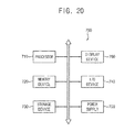
- FIG. 20 illustrates an embodiment of a mobile device 700 which includes a processor 710, a memory device 720, a storage device 730, an input/output (I/O) device 740, a power supply 750, and an electroluminescent display device 760.
- the mobile device 700 may further include a plurality of ports for communicating a video card, a sound card, a memory card, a universal serial bus (USB) device, or other electronic systems.
- USB universal serial bus
- the processor 710 performs various computing functions or tasks.
- the processor 710 may be for example, a microprocessor, a central processing unit (CPU), etc.
- the processor 710 may be connected to other components via an address bus, a control bus, a data bus, etc. Further, the processor 710 may be coupled to an extended bus such as a peripheral component interconnection (PCI) bus.
- PCI peripheral component interconnection
- the memory device 720 may store data for operations of the mobile device 700.
- the memory device 720 may include at least one non-volatile memory device such as an erasable programmable read-only memory (EPROM) device, an electrically erasable programmable read-only memory (EEPROM) device, a flash memory device, a phase change random access memory (PRAM) device, a resistance random access memory (RRAM) device, a nano-floating gate memory (NFGM) device, a polymer random access memory (PoRAM) device, a magnetic random access memory (MRAM) device, a ferroelectric random access memory (FRAM) device, and/or at least one volatile memory device such as a dynamic random access memory (DRAM) device, a static random access memory (SRAM) device, a mobile dynamic random access memory (mobile DRAM) device, etc.
- DRAM dynamic random access memory
- SRAM static random access memory
- mobile DRAM mobile dynamic random access memory
- the storage device 730 may be, for example, a solid state drive (SSD) device, a hard disk drive (HDD) device, a CD-ROM device, etc.
- the I/O device 740 may be, for example, an input device such as a keyboard, a keypad, a mouse, a touch screen, and/or an output device such as a printer, a speaker, etc.
- the power supply 750 may supply power for operating the mobile device 700.
- the electroluminescent display device 760 may communicate with other components via the buses or other communication links.
- the present embodiments may be applied to any mobile device or any computing device.
- the present embodiments may be applied to a cellular phone, a smart phone, a tablet computer, a personal digital assistant (PDA), a portable multimedia player (PMP), a digital camera, a music player, a portable game console, a navigation system, a video phone, a personal computer (PC), a server computer, a workstation, a tablet computer, a laptop computer, etc.
- the methods, processes, and/or operations described herein may be performed by code or instructions to be executed by a computer, processor, controller, or other signal processing device.
- the computer, processor, controller, or other signal processing device may be those described herein or one in addition to the elements described herein. Because the algorithms that form the basis of the methods (or operations of the computer, processor, controller, or other signal processing device) are described in detail, the code or instructions for implementing the operations of the method embodiments may transform the computer, processor, controller, or other signal processing device into a special-purpose processor for performing the methods described herein.
- calculation units, providing units, calculators, and other processing or control features of the disclosed embodiments may be implemented in logic which, for example, may include hardware, software, or both.
- the calculation units, providing units, calculators, and other processing or control features may be, for example, any one of a variety of integrated circuits including but not limited to an application-specific integrated circuit, a field-programmable gate array, a combination of logic gates, a system-on-chip, a microprocessor, or another type of processing or control circuit.
- the embodiments described herein may include, for example, a memory or other storage device for storing code or instructions to be executed, for example, by a computer, processor, microprocessor, controller, or other signal processing device.
- the computer, processor, microprocessor, controller, or other signal processing device may be those described herein or one in addition to the elements described herein. Because the algorithms that form the basis of the methods (or operations of the computer, processor, microprocessor, controller, or other signal processing device) are described in detail, the code or instructions for implementing the operations of the method embodiments may transform the computer, processor, controller, or other signal processing device into a special-purpose processor for performing the methods described herein.
- the method of extracting average current may compensate the image degradation of the display panel DP by providing the pixel average current information PAI for each of the pixels based on the average current DAI of the display panel DP.
Landscapes
- Engineering & Computer Science (AREA)
- Physics & Mathematics (AREA)
- Computer Hardware Design (AREA)
- General Physics & Mathematics (AREA)
- Theoretical Computer Science (AREA)
- Control Of El Displays (AREA)
- Control Of Indicators Other Than Cathode Ray Tubes (AREA)
Abstract
Description
- The invention relates to a method of determining average current and a method of compensating image information, and an image information compensation device.
- As the emitting time of an organic light-emitting diode increases, luminous efficiency may decrease. This may cause display quality to be adversely affected.
- In accordance with one or more embodiments, a method for extracting average current includes calculating an on-pixel ratio based on gamma information corresponding to image information, the on-pixel ratio based on turned-on pixels of a plurality of pixels in a display panel; providing maximum current information based on a dimming level; calculating an average current of the display panel based on the on-pixel ratio and the maximum current information; and providing pixel average current information for each of the pixels, the pixel average current information determined based on the average current of the display panel. The pixel average current information may be determined based on a pixel average current look-up table.
- The method may include updating the pixel average current information in the pixel average current look-up table at a predetermined time interval. The predetermined time interval may be a predetermined frame interval. After the predetermined frame interval, the pixel average current information may not be updated when a current of a corresponding one of the pixels is o. After the predetermined frame interval, the pixel average current information may be updated when a current of a corresponding one of the pixels is not o.
- The method may include storing the maximum current information corresponding to the dimming level in a max current look-up table. The method may include increasing a maximum current value corresponding to the maximum current information as the dimming level decreases. The method may include storing the maximum current information corresponding to the dimming level in the maximum current look-up table before the display panel operates. An average current of the display panel may be less than or equal to a maximum current value corresponding to the maximum current information.
- The method may include increasing the average current of the display panel as the on-pixel ratio increases. The method may include increasing the average current of the display panel as the maximum current value corresponding to the maximum current information increases. The method may include determining the average current of the display panel based on a value obtained by multiplying the on-pixel ratio and the maximum current value corresponding to the maximum current information.
- The method may include calculating a light emitting area of the display panel; and changing the pixel average current look-up table based on the light emitting area of the display panel. Deviation among the pixel average current information for the pixels may be directly proportional to the light emitting area of the display panel.
- In accordance with one or more other embodiments, a method for compensating image information includes calculating an on-pixel ratio based on gamma information corresponding to image information, the on-pixel ratio based on turned-on pixels among a plurality of pixels in a display panel; providing maximum current information corresponding to a dimming level; calculating an average current of the display panel based on the on-pixel ratio and the maximum current information; determining pixel average current information for each of the pixels based on the average current of the display panel; and compensating the gamma information corresponding to the image information based on the pixel average current information for each of the pixels.
- The method may include generating a compensation constant for compensating the gamma information based on the pixel average current information for each of the pixels. The method may include storing the pixel average current information for each of the pixels in a pixel average current look-up table; and updating the pixel average current information in the pixel average current look-up table at a predetermined time interval. The method may include storing the maximum current information corresponding to the dimming level in a maximum current look-up table, and increasing a maximum current value corresponding to the maximum current information as the dimming level decreases.
- In accordance with one or more other embodiments, an apparatus includes an on-pixel calculator to calculate an on-pixel ratio based on gamma information corresponding to image information, the on-pixel ratio based on turned-on pixels among a plurality of in a display panel; a maximum current information provider to provide maximum current information corresponding to a dimming level; an average current calculator to calculate an average current of the display panel based on the on-pixel ratio and the maximum current information; and a pixel information provider to provide pixel average current information for each of the pixels, the pixel average current information determined based on the average current of the display panel.
- In accordance with another aspect, there is provided an image information compensation device comprising an on-pixel ratio calculation unit for calculating an on-pixel ratio based on gamma information corresponding to image information, the on-pixel ratio comprising the ratio of turned-on pixels to the total of turned-on and turned-off pixels in a display panel, a maximum current information providing unit for providing a maximum current value, an average current calculation unit for calculating the average current of the display panel from the on-pixel ratio and the provided maximum current value, a pixel average current information providing unit for providing pixel average current information for each of the pixels corresponding to the average current of the display panel and a gamma information compensation unit for generating compensated values of gamma information using the pixel average current information.
- Features will become apparent to those of skill in the art by describing in detail exemplary embodiments with reference to the attached drawings in which:
-
FIG. 1 illustrates an embodiment of a method for extracting average current; -
FIG. 2 illustrates an embodiment of an average current extraction device; -
FIGS. 3 and4 illustrate examples of degradation based on pixel average current; -
FIG. 5 illustrates an example of a pixel average current look-up table; -
FIG. 6 illustrates an example of updating pixel average current information; -
FIGS. 7 and8 illustrate additional examples of updating pixel average current information; -
FIG. 9 illustrates an example of a max current look-up table; -
FIG. 10 illustrates an example of a max current value corresponding to max current information; -
FIGS. 11 and12 illustrate examples for describing average current of a display panel based on on-pixel ratio; -
FIG. 13 illustrates another embodiment of an average current extraction device; -
FIGS. 14 to 16 illustrate examples of a pixel average current look-up table based on light emitting area; and -
FIG. 17 illustrates illustrating an embodiment of a method for compensating image information. -
FIG. 18 illustrates an embodiment of an image information compensation device; -
FIG. 19 illustrates an embodiment of a display device; and -
FIG. 20 illustrates an embodiment of a mobile device. - Referring to
FIGS. 1 and2 , an average current extraction (determination)device 10 includes an on-pixel calculation unit 100, a max currentinformation providing unit 300, an averagecurrent calculation unit 500 and a pixelinformation providing unit 200. - In the method for extracting (or determining) an average current, the on-
pixel calculation unit 100 calculates an on-pixel ratio OPR using, for example, gamma information GI corresponding to image information IMI (S100). The on-pixel ratio OPR corresponds to turned-on pixels in a display panel DP. As will be described inFIGS. 10 to 12 , the pixels in the display panel DP may be turned-on based on the gamma information GI corresponding to the image information IMI. For example, in case all pixels in the display panel DP display white, the on-pixel ratio OPR is 1 or 100%. In the case where half of the pixels in the display panel DP display white, the on-pixel ratio OPR is 0.5 or 50%. In the case where three quarters of the pixels in the display panel DP display white, the on-pixel ratio OPR is 0.75 or 75%. - The max current
information providing unit 300 provides max current information MCI corresponding to a dimming level DL (S110). The max current information MCI may be, for example, a max current MC corresponding to the dimming level DL. As will be described with reference toFIG. 9 , the max current information MCI of the display panel DP may be changed according to the dimming level DL of the display device including the display panel DP. As the dimming level DL decreases, the max current MC corresponding to the max current information MCI of the display panel DP may increase. For example, when dimming level DL of the display device including the display panel DP is 3, the max current MC corresponding to the max current information MCI of the display panel DP may be 10. When the dimming level DL is 1, the max current MC corresponding to the max current information MCI of the display panel DP may be 100. - The average
current calculation unit 500 calculates an average current DAI of the display panel DP based on the on-pixel ratio OPR and the max current information MCI (S120). The average current DAI of the display panel DP may be a value based on multiplying the on-pixel ratio OPR and the max current MC value corresponding to the max current information MCI. For example, the on-pixel ratio OPR may be 1 and the dimming level DL may be 1. When the dimming level DL is 1, the max current MC corresponding to the max current information MCI may be 100. In this case, the average current DAI of the display panel DP is 100, which is the value obtained by multiplying the on-pixel ratio OPR and the max current MC value. - In another example, the on-pixel ratio OPR may be 0.5 and the dimming level DL may be 1. When the dimming level DL is 1, the max current MC corresponding to the max current information MCI is 100. In this case, the average current DAI of the display panel DP is 50, which is the value obtained by multiplying the on-pixel ratio OPR and the max current MC value.
- In another example, the on-pixel ratio OPR may be 0.5 and the dimming level DL may be 3. When the dimming level DL is 3, the max current MC corresponding to the max current information MCI may be 10. In this case, the average current DAI of the display panel DP is 5, which is the value obtained by multiplying the on-pixel ratio OPR and the max current MC value.
- The pixel
information providing unit 200 provides pixel average current information PAI for each of the pixels (S130). The pixel average current information PAI is determined by the average current DAI of the display panel DP. As will be described with reference toFIG. 5 , the pixel average current PAC for each of the pixels may be changed according to the average current DAI of the display panel DP. When the average current DAI of the display panel DP is determined, the pixel average current PAC for each of the pixels in the display panel DP may be determined. The pixel average current information PAI for each of the pixels in the display panel DP may be stored in a pixel average current look-up table PACLT. - The method for extracting average current may compensate the image degradation of the display panel DP by providing the pixel average current information PAI for each of the pixels based on the average current DAI of the display panel DP.
-
FIGS. 3 and4 illustrate examples for describing degradation based on pixel average current PAC. Referring toFIGS. 3 and4 , when atransistor 75 is turned-on based on the data voltage DV, current is transferred through an organic light-emittingdiode 76. The degree of degradation of the pixel may be different according to the pixel average current PAC transferred through the organic light-emittingdiode 76. For example, the pixel average current PAC transferred through the organic light-emittingdiode 76 may be a first pixel average current PAC1. The pixel average current PAC transferred through the organic light-emittingdiode 76 may be a second pixel average current PAC2. The pixel average current PAC transferred through the organic light-emittingdiode 76 may be a third pixel average current PAC3. The first pixel average current PAC1 may be greater than the second pixel average current PAC2. The second pixel average current PAC2 may be greater than the third pixel average current PAC3. - The degree of degradation of the pixel may increase as the pixel average current PAC transferred through the organic light-emitting
diode 76 increases. For example, when the pixel average current PAC transferred through the organic light-emittingdiode 76 is the first pixel average current PAC1, the degree of degradation of the pixel may be highest. When the pixel average current PAC transferred through the organic light-emittingdiode 76 is the second pixel average current PAC2, the degree of degradation of the pixel may be second highest. When the pixel average current PAC transferred through the organic light-emittingdiode 76 is the third pixel average current PAC3, the degree of degradation of the pixel may be lowest. The degree of degradation of the pixel may be different according to the pixel average current PAC transferred through the organic light-emittingdiode 76. -
FIG. 5 illustrates an example corresponding to a pixel average current look-up table. Referring toFIG. 5 , the pixel average current PAC for each of the pixels may be changed according to the average current DAI of the display panel DP. When the average current DAI of the display panel DP is determined, the pixel average current PAC for each of the pixels in the display panel DP may be determined. The pixel average current information PAI for each of the pixels in the display panel DP may be stored in a pixel average current look-up table PACLT. - For example, the average current DAI of the display panel DP may be a first average current DAC1. In this case, as the pixel address is increased, the pixel average current PAC may be increased after the pixel average current PAC is decreased. The average current DAI of the display panel DP may be a second average current DAC2. In this case, as the pixel address is increased, the pixel average current PAC may be increased after the pixel average current PAC is decreased. Also, in this case, the range of the pixel average current PAC in the second average current DAC2 may be less than the range of the pixel average current PAC in the first average current DAC1. The average current DAI of the display panel DP may be a third average current DAC3. In this case, as the pixel address is increased, the pixel average current PAC may be constant.
- The pixel average current information PAI for each of the pixels according to the average current DAI of the display panel DP may be stored in a pixel average current look-up table PACLT. In one embodiment, the pixel
information providing unit 200 may include the pixel average current look-up table PACLT for storing pixel average current information PAI for each of the pixels. - The method for extracting average current may compensate image degradation of the display panel DP by providing the pixel average current information PAI for each of the pixels based on the average current DAI of the display panel DP.
-
FIG. 6 illustrates an example for updating pixel average current in the pixel average current look-up table PACLT. Referring toFIG. 6 , the pixel average current information PAI in the pixel average current look-up table PACLT may be updated at predetermined time intervals PDT. For example, in a first time T1, the averagecurrent extraction device 10 may update the pixel average current information PAI in the pixel average current look-up table PACLT based on a first pixel current PC1. The first pixel current PC1 may be a current transferred to the organic light-emittingdiode 76 in the first time T1. In a second time T2, the averagecurrent extraction device 10 may update the pixel average current information PAI in the pixel average current look-up table PACLT based on a second pixel current PC2. The second pixel current PC2 may be a current transferred to the organic light-emittingdiode 76 in the second time T2. In a third time T3, the averagecurrent extraction device 10 may update the pixel average current information PAI in the pixel average current look-up table PACLT based on a third pixel current PC. The third pixel current PC may be a current transferred to the organic light-emittingdiode 76 in the third time T3. The time interval between the first time T1 and the second time T2 may be the predetermined time interval PDT. Also, the time interval between the second time T2 and the third time T3 may be the predetermined time interval PDT. These intervals may be different in another embodiment. - The method for extracting average current may compensate image degradation of the display panel DP by providing the pixel average current information PAI for each of the pixels based on the average current DAI of the display panel DP.
-
FIGS. 7 and8 illustrate additional examples for updating pixel average current information in a pixel average current look-up table. Referring toFIGS. 7 and8 , the predetermined time interval PDT may be a predetermined frame interval. In this embodiment, the pixel average current look-up table PACLT may be updated. After the predetermined frame interval, when a current of the pixel is 0, the pixel average current information PAI for the pixel may not be updated. For example, the predetermined frame interval may be one frame interval. - In a first frame F1, the first pixel current PC1 transferred to the organic light-emitting
diode 76 in the first pixel PIXEL1 may be 5. In this case, the first pixel average current PAC1 may be 5. When the first pixel average current PAC1 is 5, the pixel average current information PAI corresponding to the first pixel average current PAC1 in the pixel average current look-up table PACLT may be updated to 5. - In a second frame F2, the second pixel current PC2 transferred to the organic light-emitting
diode 76 in the first pixel PIXEL1 may be o. In case the first pixel current PC1 that is transferred to the organic light-emittingdiode 76 included in the first pixel PIXEL1 is 0 in the first frame F1, the second pixel average current PAC2 may be 5. After the predetermined frame interval, when the current of the pixel is 0, the pixel average current information PAI for the pixel may not be updated. - In one embodiment, the pixel average current look-up table PACLT may be updated. After the predetermined frame interval, if the current of the pixel is not 0, the pixel average current information PAI for the pixel may be updated.
- For example, in a third frame F3, the third pixel current PC transferred to the organic light-emitting
diode 76 in the first pixel PIXEL1 may be 4. In case the third pixel current PC that is transferred to the organic light-emittingdiode 76 included in the first pixel PIXEL1 is 4 in the third frame F3, the third pixel average current PAC3 may be (5+4)/3=3. When the third pixel average current PAC3 is 3, the pixel average current information PAI corresponding to the third pixel average current PAC3 in the pixel average current look-up table PACLT may be updated to 3. - As a result, the pixel average current information PAI for the first pixel PIXEL1 may be updated to 5 in the first frame F1. The pixel average current information PAI for the first pixel PIXEL1 may not be updated in the second frame F2. The pixel average current information PAI for the first pixel PIXEL1 may be updated to 3 in the third frame F3.
- The method for extracting average current may compensate image degradation of the display panel DP by providing the pixel average current information PAI for each of the pixels based on the average current of the display panel DP.
-
FIG. 9 illustrates an example of a max current look-up table, andFIG. 10 illustrates an example for describing a max current value corresponding to max current info. Referring toFIG. 9 , the max currentinformation providing unit 300 may include a max current look-up table MCLT that stores the max current information MCI corresponding to the dimming level DL. The max current information MCI corresponding to the dimming level DL may be stored in the max current look-up table MCLT before the display panel DP operates. As the dimming level DL is decreased, a max current MC value corresponding to the max current information MCI may be increased. - For example, when the dimming level DL of the display device including the average
current extraction device 10 is 0, the max current MC corresponding to the max current information MCI may be 100. When the dimming level DL of the display device including the averagecurrent extraction device 10 is 1, the max current MC corresponding to the max current information MCI may be 50. - When the dimming level DL of the display device including the average
current extraction device 10 is 2, the max current MC corresponding to the max current information MCI may be 10. When the dimming level DL of the display device including the averagecurrent extraction device 10 is 3, the max current MC corresponding to the max current information MCI may be o. - Therefore, as the dimming level DL is decreased, a max current value corresponding to the max current information MCI may be increased. The max current MC corresponding to the max current information MCI may be used to calculate the average current DAI of the display panel DP.
- Referring to
FIGS. 9 and10 , the on-pixel ratio OPR may be 1. When the dimming level DL of the display device is 1, the max current MC corresponding to the max current information MCI may be 50. In this case, the average current DAI of the display panel DP may be 50. In addition, when the dimming level DL of the display device is 2, the max current MC corresponding to the max current information MCI may be 10. In this case, the average current DAI of the display panel DP may be 10. In addition, when the dimming level DL of the display device is 3, the max current MC corresponding to the max current information MCI may be o. In this case, the average current DAI of the display panel DP may be o. -
FIGS. 11 and12 illustrate examples for describing average current of a display panel according to an on-pixel ratio. Referring toFIGS. 9 ,11 , and12 , an average current DAI of the display panel DP may be less than or equal to a max current MC value corresponding to the max current information MCI. For example, when the on-pixel ratio OPR is 1, the average current DAI of the display panel DP may be equal to the max current MC corresponding to the max current information MCI. When the on-pixel ratio OPR is less than 1, the average current DAI of the display panel DP may be less than the max current MC corresponding to the max current information MCI. - In one embodiment, as the on-pixel ratio OPR is increased, the average current DAI of the display panel DP may be increased. For example, when the dimming level DL of the display device is 0, the max current MC corresponding to the max current information MCI may be 100. When the dimming level DL of the display device is 0 and the on-pixel ratio OPR is 0.5, the average current DAI of the display panel DP may be 50. When the dimming level DL of the display device is 3 and the on-pixel ratio OPR is 0.75, the average current DAI of the display panel DP may be 75. Therefore, as the on-pixel ratio OPR is increased, the average current DAI of the display panel DP is increased.
- In one embodiment, as the max current MC value corresponding to the max current information MCI is increased, the average current DAI of the display panel DP may be increased. For example, the on-pixel ratio OPR may be 0.5 and the dimming level DL may be 1. When the dimming level DL is 1, the max current MC corresponding to the max current information MCI may be 50. In this case, the average current DAI of the display panel DP may be 25.
- In another example, the on-pixel ratio OPR may be 0.5 and the dimming level DL may be 2. When the dimming level DL is 2, the max current MC corresponding to the max current information MCI may be 10. In this case, the average current DAI of the display panel DP may be 5.
- In another example, the on-pixel ratio OPR may be 0.5 and the dimming level DL may be o.
- When the dimming level DL is 0, the max current MC corresponding to the max current information MCI may be 100. In this case, the average current DAI of the display panel DP may be 50. The average current DAI of the display panel DP may be a value obtained by multiplying the on-pixel ratio OPR and the max current MC value corresponding to the max current information MCI.
- The method for extracting average current may compensate image degradation of the display panel DP by providing the pixel average current information PAI for each of the pixels based on the average current DAI of the display panel DP.
-
FIG. 13 illustrates another embodiment of an average current extraction device, andFIGS. 14 to 16 illustrate examples corresponding to a pixel average current look-up table according to a light emitting area. - Referring to
FIG. 13 , an averagecurrent extraction device 10a includes an on-pixel calculation unit 100, a max currentinformation providing unit 300, an averagecurrent calculation unit 500, and a pixelinformation providing unit 200. The on-pixel calculation unit 100 calculates an on-pixel ratio OPR based on a gamma information GI corresponding to image information IMI. The on-pixel ratio OPR corresponds to turned-on pixels among pixels in a display panel DP. A max currentinformation providing unit 300 provides a max current information MCI corresponding to a dimming level DL. - The average
current calculation unit 500 calculates an average current of the display panel DP based on the on-pixel ratio OPR and the max current information MCI. - The pixel
information providing unit 200 provides a pixel average current information PAI for each of the pixels. The pixel average current information PAI is determined by the average current DAI of the display panel DP. - In one embodiment, a display device including the display panel DP may include a light emitting
area calculator 400 to calculate a light emitting area LEA of the display panel DP. - Referring to
FIGS. 14 to 16 , the pixelinformation providing unit 200 may change the pixel average current look-up table PACLT based on the light emitting area LEA of the display panel DP. For example, the average current DAI of the display panel DP may be the first average current DAC1. In this case, the pixel average current look-up table PACLT according to the light emitting area LEA may be generated based on the curve for the first average current DAC1 ofFIG. 5 . - For example, when the light emitting area LEA is 90%, the pixel average current look-up table PACLT may be similar to the curve for the first average current DAC1 of
FIG. 5 . As the light emitting area LEA is decreased, the range of the pixel average current PAC value corresponding to the pixel average current information PAI stored in the pixel average current look-up table PACLT may be decreased. For example, as the light emitting area LEA of the display panel DP is decreased, a deviation among the pixel average current information PAI for the pixels may be decreased. The pixel average current look-up table PACLT may be separately generated for each of the light emitting areas. - The method for extracting average current may compensate image degradation of the display panel DP by providing the pixel average current information PAI for each of the pixels based on the average current DAI of the display panel DP.
-
FIG. 17 illustrates an embodiment of a method for compensating image information, andFIG. 18 illustrates an embodiment of an imageinformation compensation device 15. Referring toFIGS. 17 and18 , the imageinformation compensation device 15 includes an on-pixel calculation unit 100, a max currentinformation providing unit 300, an averagecurrent calculation unit 500, a pixelinformation providing unit 200 and a compensationconstant generator 210. - In the method for compensating image information, the on-
pixel calculation unit 100 calculates an on-pixel ratio OPR based on a gamma information GI corresponding to image information IMI (S200). The on-pixel ratio OPR corresponds to turned-on pixels among pixels in the display panel DP. The on-pixel ratio OPR corresponds to turned-on pixels among pixels included in a display panel DP. As will be described with reference toFIGS. 10 to 12 , the pixels in the display panel DP may be turned-on based the gamma information GI corresponding to the image information IMI. - For example, when all pixels in the display panel DP display white color based the gamma information GI corresponding to the image information IMI, the on-pixel ratio OPR may be 1 or 100%. When half of the pixels in the display panel DP display white color based the gamma information GI corresponding to the image information IMI, the on-pixel ratio OPR may be 0.5 or 50%. When three quarters of the pixels in the display panel DP display white color based the gamma information GI corresponding to the image information IMI, the on-pixel ratio OPR may be 0.75 or 75%.
- The max current
information providing unit 300 provides a max current information MCI corresponding to a dimming level DL (S210). The max current information MCI may be a max current MC value corresponding to the dimming level DL. The max current information MCI of the display panel DP may be changed according to the dimming level DL of the display device including the display panel DP. As the dimming level DL is decreased, the max current MC corresponding to the max current information MCI of the display panel DP may be increased. For example, when the dimming level DL is 1, the max current MC corresponding to the max current information MCI of the display panel DP may be 50. When the dimming level DL is 3, the max current MC corresponding to the max current information MCI of the display panel DP may be o. - The average
current calculation unit 500 calculates an average current DAI of the display panel DP based on the on-pixel ratio OPR and the max current information MCI (S220). The average current DAI may be a value obtained by multiplying the on-pixel ratio OPR and the max current MC value corresponding to the max current information MCI. For example, the on-pixel ratio OPR may be 1 and the dimming level DL may be 1. When the dimming level DL is 1, the max current MC corresponding to the max current information MCI may be 50. In this case, the average current DAI of the display panel DP may be 50. The value obtained by multiplying the on-pixel ratio OPR and the max current MC value corresponding to the max current information MCI may be 50. - In addition, the on-pixel ratio OPR may be 0.5 and the dimming level DL may be 1. When the dimming level DL is 1, the max current MC corresponding to the max current information MCI may be 50. In this case, the average current DAI of the display panel DP may be 25. The value obtained by multiplying the on-pixel ratio OPR and the max current MC value corresponding to the max current information MCI may be 25.
- In addition, the on-pixel ratio OPR may be 0.5 and the dimming level DL may be o. In case the dimming level DL is 0, the max current MC corresponding to the max current information MCI may be 100. In this case, the average current DAI of the display panel DP may be 50. The value obtained by multiplying the on-pixel ratio OPR and the max current MC value corresponding to the max current information MCI may be 50.
- The pixel
information providing unit 200 provides a pixel average current information PAI for each of the pixels (S230). The pixel average current information PAI is determined by the average current DAI of the display panel DP. The pixel average current PAC for each of the pixels may be changed according to the average current DAI of the display panel DP. When the average current DAI of the display panel DP is determined, the pixel average current PAC for each of the pixels in the display panel DP may be determined. The pixel average current information PAI for each of the pixels in the display panel DP may be stored in a pixel average current look-up table PACLT. - The gamma information GI corresponding to the image information IMI is compensated based on the pixel average current information PAI for each of the pixels (S240). In one embodiment, a display device including the display panel DP may include a compensation
constant generator 210 that generates a compensation constant CC of compensating the gamma information GI based on the pixel average current information PAI for each of the pixels. For example, the gamma information GI corresponding to the image information IMI may be compensated using the compensation constant CC generated from the compensationconstant generator 210. For example, the compensation constant CC may be applied to a data voltage to compensate the data voltage. - In one embodiment, the pixel
information providing unit 200 includes a pixel average current look-up table PACLT that stores the pixel average current information PAI for each of the pixels. The pixel average current information PAI in the pixel average current look-up table PACLT may be updated every a predetermined time interval PDT. The pixel average current PAC for each of the pixels may be changed according to the average current DAI of the display panel DP. When the average current DAI of the display panel DP is determined, the pixel average current PAC for each of the pixels in the display panel DP may be determined. The pixel average current information PAI for each of the pixels in the display panel DP may be stored in a pixel average current look-up table PACLT. - For example, in a first time T1, the average
current extraction device 10 may update the pixel average current information PAI in the pixel average current look-up table PACLT based on a first pixel current PC1. The first pixel current PC1 may be a current transferred to the organic light-emittingdiode 76 in the first time T1. - In a second time T2, the average
current extraction device 10 may update the pixel average current information PAI in the pixel average current look-up table PACLT based on a second pixel current PC2. The second pixel current PC2 may be a current transferred to the organic light-emittingdiode 76 in the second time T2. - In a third time T3, the average
current extraction device 10 may update the pixel average current information PAI in the pixel average current look-up table PACLT based on a third pixel current PC. The third pixel current PC may be a current transferred to the organic light-emittingdiode 76 in the third time T3. The time interval between the first time T1 and the second time T2 may be the predetermined time interval PDT. The time interval between the second time T2 and the third time T3 may be the predetermined time interval PDT. The time intervals may be different in another embodiment. - In one embodiment, the max current
information providing unit 300 may include a max current look-up table MCLT for storing the max current information MCI corresponding to the dimming level DL. As the dimming level DL is decreased, a max current MC value corresponding to the max current information MCI may be increased. The max current information MCI corresponding to the dimming level DL may be stored in the max current look-up table MCLT before the display panel DP operates. - For example, when the dimming level DL of the display device including the average
current extraction device 10 is 0, the max current MC corresponding to the max current information MCI may be 100. When the dimming level DL is 1, the max current MC corresponding to the max current information MCI may be 50. When the dimming level DL is 2, the max current MC corresponding to the max current information MCI may be 10. When the dimming level DL is 3, the max current MC corresponding to the max current information MCI may be o. Therefore, as the dimming level DL is decreased, a max current MC value corresponding to the max current information MCI may be increased. The max current MC corresponding to the max current information MCI may be used as a basis for calculating the average current DAI of the display panel DP. - The method for extracting average current may compensate the image degradation of the display panel DP by providing the pixel average current information PAI for each of the pixels based on the average current DAI of the display panel DP.
-
FIG. 19 illustrates an embodiment of adisplay device 20 which includes agamma unit 230, a compensationconstant generator 210, acompensation unit 250 and a display panel DP. Thegamma unit 230 provides the gamma information GI corresponding to image information IMI. The compensationconstant generator 210 generates the compensation constant CC that compensates the gamma information GI based on the pixel average current information PAI. Thecompensation unit 250 provides the compensation gamma information CGI based on the gamma information GI and the compensation constant CC. The display panel DP display an image based on the compensation gamma information CGI. -
FIG. 20 illustrates an embodiment of amobile device 700 which includes aprocessor 710, amemory device 720, astorage device 730, an input/output (I/O)device 740, apower supply 750, and anelectroluminescent display device 760. Themobile device 700 may further include a plurality of ports for communicating a video card, a sound card, a memory card, a universal serial bus (USB) device, or other electronic systems. - The
processor 710 performs various computing functions or tasks. Theprocessor 710 may be for example, a microprocessor, a central processing unit (CPU), etc. Theprocessor 710 may be connected to other components via an address bus, a control bus, a data bus, etc. Further, theprocessor 710 may be coupled to an extended bus such as a peripheral component interconnection (PCI) bus. - The
memory device 720 may store data for operations of themobile device 700. For example, thememory device 720 may include at least one non-volatile memory device such as an erasable programmable read-only memory (EPROM) device, an electrically erasable programmable read-only memory (EEPROM) device, a flash memory device, a phase change random access memory (PRAM) device, a resistance random access memory (RRAM) device, a nano-floating gate memory (NFGM) device, a polymer random access memory (PoRAM) device, a magnetic random access memory (MRAM) device, a ferroelectric random access memory (FRAM) device, and/or at least one volatile memory device such as a dynamic random access memory (DRAM) device, a static random access memory (SRAM) device, a mobile dynamic random access memory (mobile DRAM) device, etc. - The
storage device 730 may be, for example, a solid state drive (SSD) device, a hard disk drive (HDD) device, a CD-ROM device, etc. The I/O device 740 may be, for example, an input device such as a keyboard, a keypad, a mouse, a touch screen, and/or an output device such as a printer, a speaker, etc. Thepower supply 750 may supply power for operating themobile device 700. Theelectroluminescent display device 760 may communicate with other components via the buses or other communication links. - The present embodiments may be applied to any mobile device or any computing device. For example, the present embodiments may be applied to a cellular phone, a smart phone, a tablet computer, a personal digital assistant (PDA), a portable multimedia player (PMP), a digital camera, a music player, a portable game console, a navigation system, a video phone, a personal computer (PC), a server computer, a workstation, a tablet computer, a laptop computer, etc.
- The methods, processes, and/or operations described herein may be performed by code or instructions to be executed by a computer, processor, controller, or other signal processing device. The computer, processor, controller, or other signal processing device may be those described herein or one in addition to the elements described herein. Because the algorithms that form the basis of the methods (or operations of the computer, processor, controller, or other signal processing device) are described in detail, the code or instructions for implementing the operations of the method embodiments may transform the computer, processor, controller, or other signal processing device into a special-purpose processor for performing the methods described herein.
- The calculation units, providing units, calculators, and other processing or control features of the disclosed embodiments may be implemented in logic which, for example, may include hardware, software, or both. When implemented at least partially in hardware, the calculation units, providing units, calculators, and other processing or control features may be, for example, any one of a variety of integrated circuits including but not limited to an application-specific integrated circuit, a field-programmable gate array, a combination of logic gates, a system-on-chip, a microprocessor, or another type of processing or control circuit.
- When implemented at least partially in software, the embodiments described herein may include, for example, a memory or other storage device for storing code or instructions to be executed, for example, by a computer, processor, microprocessor, controller, or other signal processing device. The computer, processor, microprocessor, controller, or other signal processing device may be those described herein or one in addition to the elements described herein. Because the algorithms that form the basis of the methods (or operations of the computer, processor, microprocessor, controller, or other signal processing device) are described in detail, the code or instructions for implementing the operations of the method embodiments may transform the computer, processor, controller, or other signal processing device into a special-purpose processor for performing the methods described herein.
- In accordance with one or more embodiments, the method of extracting average current may compensate the image degradation of the display panel DP by providing the pixel average current information PAI for each of the pixels based on the average current DAI of the display panel DP.
- Example embodiments have been disclosed herein, and although specific terms are employed, they are used and are to be interpreted in a generic and descriptive sense only and not for purpose of limitation. In some instances, as would be apparent to one of skill in the art as of the filing of the present application, features, characteristics, and/or elements described in connection with a particular embodiment may be used singly or in combination with features, characteristics, and/or elements described in connection with other embodiments unless otherwise indicated. Accordingly, it will be understood by those of skill in the art that various changes in form and details may be made without departing from the scope of the invention as set forth in the following claims.
Claims (15)
- A method of compensating image information, the method comprising:calculating an on-pixel ratio based on gamma information corresponding to image information, the on-pixel ratio based on turned-on pixels of a plurality of pixels in a display panel;providing maximum current information;calculating an average current of the display panel based on the on-pixel ratio and the maximum current information;providing pixel average current information for each of the pixels based on the average current of the display panel; andgenerating compensated gamma information using the pixel average current information.
- The method as claimed in claim 1, wherein the pixel average current information is determined from a pixel average current look-up table.
- The method as claimed in claim 2, further comprising:updating the pixel average current information in the pixel average current look-up table at a predetermined time interval.
- The method as claimed in claim 3, wherein the predetermined time interval is a predetermined frame interval.
- The method as claimed in claim 4, wherein, after the predetermined frame interval, the pixel average current information is not updated when a current of a corresponding one of the pixels is zero and/or wherein after the predetermined frame interval, the pixel average current information is updated when a current of a corresponding one of the pixels is not zero.
- The method as claimed in any one of the preceding claims, wherein the maximum current information corresponds to a dimming level.
- The method as claimed in any one of the preceding claims, further comprising:storing the maximum current information in a maximum current look-up table.
- The method as claimed in claim 6, further comprising:increasing a maximum current value corresponding to the maximum current information as the dimming level decreases.
- The method as claimed in claim 7, further comprising:storing the maximum current information in the maximum current look-up table before the display panel operates.
- The method as claimed in any one of the preceding claims, wherein an average current of the display panel is less than or equal to a maximum current value corresponding to the maximum current information, and/or further comprising increasing the average current of the display panel as the on-pixel ratio increases, and/or further comprising increasing the average current of the display panel as the maximum current value corresponding to the maximum current information increases.
- The method as claimed in any one of the preceding claims, further comprising:determining the average current of the display panel by multiplying the on-pixel ratio and a maximum current value corresponding to the maximum current information.
- The method as claimed in claim 2, further comprising:calculating a light emitting area of the display panel; andchanging the pixel average current look-up table based on the light emitting area of the display panel.
- The method as claimed in claim 12, wherein deviation among the pixel average current information for the pixels is directly proportional to the light emitting area of the display panel.
- An image information compensation device comprising:an on-pixel ratio calculation unit for calculating an on-pixel ratio based on gamma information corresponding to image information, the on-pixel ratio comprising the ratio of turned-on pixels to the total of turned-on and turned-off pixels in a display panel;a maximum current information providing unit for providing a maximum current value;an average current calculation unit for calculating the average current of the display panel from the on-pixel ratio and the provided maximum current value;a pixel average current information providing unit for providing pixel average current information for each of the pixels corresponding to the average current of the display panel; anda gamma information compensation unit for generating compensated values of gamma information using the pixel average current information.
- A display device comprising a display panel and an image information compensation device according to claim 14.
Applications Claiming Priority (1)
| Application Number | Priority Date | Filing Date | Title |
|---|---|---|---|
| KR1020150012538A KR102288794B1 (en) | 2015-01-27 | 2015-01-27 | Method of extracting average current and method of compensating image information including the same |
Publications (1)
| Publication Number | Publication Date |
|---|---|
| EP3051528A1 true EP3051528A1 (en) | 2016-08-03 |
Family
ID=54293045
Family Applications (1)
| Application Number | Title | Priority Date | Filing Date |
|---|---|---|---|
| EP15187582.0A Ceased EP3051528A1 (en) | 2015-01-27 | 2015-09-30 | Method of compensating image information and image information compensation device |
Country Status (4)
| Country | Link |
|---|---|
| US (2) | US10121417B2 (en) |
| EP (1) | EP3051528A1 (en) |
| KR (1) | KR102288794B1 (en) |
| CN (1) | CN105825810B (en) |
Families Citing this family (7)
| Publication number | Priority date | Publication date | Assignee | Title |
|---|---|---|---|---|
| TWI566229B (en) * | 2015-06-03 | 2017-01-11 | 友達光電股份有限公司 | Timing controller of display device and a method thereof |
| KR102449369B1 (en) * | 2015-12-07 | 2022-10-04 | 삼성디스플레이 주식회사 | Display device and method of testing a display device |
| KR102561188B1 (en) * | 2016-09-22 | 2023-07-28 | 삼성디스플레이 주식회사 | Display Device |
| US11501694B2 (en) | 2020-02-12 | 2022-11-15 | Samsung Display Co., Ltd. | Display device and driving method thereof |
| US12293731B2 (en) * | 2021-12-17 | 2025-05-06 | Apple Inc. | Emission profile tracking for electronic displays |
| US12175950B2 (en) | 2022-09-26 | 2024-12-24 | Samsung Electronics Co., Ltd. | Electronic device, method, and non-transitory computer readable storage medium identifying brightness level according to on pixel ratio |
| CN116844472B (en) * | 2023-07-20 | 2026-01-23 | 京东方科技集团股份有限公司 | Pixel data processing method, device, display equipment and storage medium |
Citations (4)
| Publication number | Priority date | Publication date | Assignee | Title |
|---|---|---|---|---|
| EP1231592A2 (en) * | 2001-02-08 | 2002-08-14 | Semiconductor Energy Laboratory Co., Ltd. | Light emitting device and electronic equipment using the same |
| US20050110786A1 (en) * | 2003-09-29 | 2005-05-26 | Masutaka Inoue | Display device |
| US20080231557A1 (en) * | 2007-03-20 | 2008-09-25 | Leadis Technology, Inc. | Emission control in aged active matrix oled display using voltage ratio or current ratio |
| US20140028734A1 (en) * | 2012-07-25 | 2014-01-30 | Sony Corporation | Display device, image processing device, and image processing method |
Family Cites Families (6)
| Publication number | Priority date | Publication date | Assignee | Title |
|---|---|---|---|---|
| KR101348753B1 (en) | 2005-06-10 | 2014-01-07 | 삼성디스플레이 주식회사 | Display device and driving method thereof |
| CA2556961A1 (en) | 2006-08-15 | 2008-02-15 | Ignis Innovation Inc. | Oled compensation technique based on oled capacitance |
| KR100914118B1 (en) | 2007-04-24 | 2009-08-27 | 삼성모바일디스플레이주식회사 | Organic electroluminescent display and driving method thereof |
| KR101310921B1 (en) * | 2009-12-29 | 2013-09-25 | 엘지디스플레이 주식회사 | Organic light emitting display device and its driving method |
| JP4966383B2 (en) * | 2010-01-13 | 2012-07-04 | 株式会社東芝 | Liquid crystal display |
| KR101965674B1 (en) | 2012-12-19 | 2019-04-04 | 엘지디스플레이 주식회사 | Driving method for organic light emitting display |
-
2015
- 2015-01-27 KR KR1020150012538A patent/KR102288794B1/en active Active
- 2015-09-30 EP EP15187582.0A patent/EP3051528A1/en not_active Ceased
- 2015-10-30 US US14/927,744 patent/US10121417B2/en active Active
- 2015-12-02 CN CN201510873016.8A patent/CN105825810B/en active Active
-
2018
- 2018-10-25 US US16/170,422 patent/US10388229B2/en active Active
Patent Citations (4)
| Publication number | Priority date | Publication date | Assignee | Title |
|---|---|---|---|---|
| EP1231592A2 (en) * | 2001-02-08 | 2002-08-14 | Semiconductor Energy Laboratory Co., Ltd. | Light emitting device and electronic equipment using the same |
| US20050110786A1 (en) * | 2003-09-29 | 2005-05-26 | Masutaka Inoue | Display device |
| US20080231557A1 (en) * | 2007-03-20 | 2008-09-25 | Leadis Technology, Inc. | Emission control in aged active matrix oled display using voltage ratio or current ratio |
| US20140028734A1 (en) * | 2012-07-25 | 2014-01-30 | Sony Corporation | Display device, image processing device, and image processing method |
Also Published As
| Publication number | Publication date |
|---|---|
| US10388229B2 (en) | 2019-08-20 |
| CN105825810B (en) | 2020-06-09 |
| US20160217745A1 (en) | 2016-07-28 |
| US10121417B2 (en) | 2018-11-06 |
| KR20160092539A (en) | 2016-08-05 |
| KR102288794B1 (en) | 2021-08-12 |
| US20190066602A1 (en) | 2019-02-28 |
| CN105825810A (en) | 2016-08-03 |
Similar Documents
| Publication | Publication Date | Title |
|---|---|---|
| US10388229B2 (en) | Method for compensating image information | |
| US10971065B2 (en) | Display device, and method of determining a power supply voltage | |
| US9947265B2 (en) | Electroluminescent display device and method of driving the same to compensate for degeneration of pixels | |
| US9666128B2 (en) | Electroluminescent display for adaptive voltage control and method of driving electroluminescent display | |
| US9542887B2 (en) | Organic light emitting display device and method of driving an organic light emitting display device | |
| KR102378190B1 (en) | Electroluminescent display device for reducing color distortion of low gray values and method of operating the same | |
| CN103680401B (en) | Gamma correction curve generation method, gamma correcting unit and display device | |
| US11217180B2 (en) | Display device, and method of determining a power supply voltage based on gray level and voltage drop | |
| US9852675B2 (en) | Data compensator to mitigate luminance distortion of display device | |
| KR102423587B1 (en) | Organic light emitting diode display device | |
| US11244590B2 (en) | Gamma voltage generator and display device | |
| US10255839B2 (en) | Driving unit, display device and method of driving a display panel | |
| US11735118B2 (en) | Organic light emitting display device and driving method of the same | |
| KR20160010680A (en) | Method of operating an organic light emitting display device and organic light emitting display device | |
| US20160063943A1 (en) | Degradation compensating pixel circuit and organic light emitting diode display device including the same | |
| US9842534B2 (en) | Display device and display system including the same | |
| US9858867B2 (en) | Method of controlling scale factor and method of controlling luminance including the same | |
| US9583039B2 (en) | Method of digitally driving organic light-emitting diode (OLED) display | |
| KR102928090B1 (en) | Display device, and method of operating a display device | |
| KR102234795B1 (en) | Method of processing image data and display system for display power reduction | |
| KR20250118918A (en) | Display device and driving the same |
Legal Events
| Date | Code | Title | Description |
|---|---|---|---|
| PUAI | Public reference made under article 153(3) epc to a published international application that has entered the european phase |
Free format text: ORIGINAL CODE: 0009012 |
|
| AK | Designated contracting states |
Kind code of ref document: A1 Designated state(s): AL AT BE BG CH CY CZ DE DK EE ES FI FR GB GR HR HU IE IS IT LI LT LU LV MC MK MT NL NO PL PT RO RS SE SI SK SM TR |
|
| AX | Request for extension of the european patent |
Extension state: BA ME |
|
| STAA | Information on the status of an ep patent application or granted ep patent |
Free format text: STATUS: REQUEST FOR EXAMINATION WAS MADE |
|
| 17P | Request for examination filed |
Effective date: 20170203 |
|
| RBV | Designated contracting states (corrected) |
Designated state(s): AL AT BE BG CH CY CZ DE DK EE ES FI FR GB GR HR HU IE IS IT LI LT LU LV MC MK MT NL NO PL PT RO RS SE SI SK SM TR |
|
| STAA | Information on the status of an ep patent application or granted ep patent |
Free format text: STATUS: EXAMINATION IS IN PROGRESS |
|
| 17Q | First examination report despatched |
Effective date: 20170512 |
|
| STAA | Information on the status of an ep patent application or granted ep patent |
Free format text: STATUS: THE APPLICATION HAS BEEN REFUSED |
|
| 18R | Application refused |
Effective date: 20190113 |